CB8 Manual
Edit this on GitLab
INTRODUCTION
As a leading manufacturer of smart function modules, NAI offers over 100 different modules that cover a wide range of I/O, measurements and simulation, communications, Ethernet switch, and SBC functions. Our CAN Bus smart function modules provide independent, isolated, channels of CAN serial data bus links, conforming to the ISO 11898 International Standard.
CAN (Controller Area Network) is a multi-master, broadcast, serial bus standard for connecting Electronic Control Units (ECUs) in the automotive, aerospace, marine, industrial automation and medical equipment industries. ISO 11898 defines the CAN serial bus system and specifies its architecture and operating parameters. Module CB8 conforms to CAN Specification 2.0, parts A and B, provides Flexible Data (FD) communication, and conforms to ARINC 825-4, which supports both CAN 2.0 and CAN FD. The CAN protocol was developed by Robert Bosch GmbH and is recognized and protected by patents and licensed by Bosch.
This user manual is designed to help you get the most out of our CAN Bus smart function modules.
For a brief description of the function and features of the CB8, click here for the CB8 Data Sheet
CB8 Overview
NAI’s CB8 modules offers a range of features designed to suit a variety of system requirements, including:
Eight Independent Fully Isolated CAN Bus Communication Channels: The CB8 provides eight independent CAN bus channels, each with full isolation to help protect against electrical noise, ground potential differences, and fault propagation. This architecture supports reliable operation across multiple networks at the same time while improving overall system robustness.
Supports ISO-11898 CAN 2.0A and CAN 2.0B Protocols: This module supports both CAN 2.0A and CAN 2.0B in accordance with ISO-11898, enabling compatibility with both 11-bit and 29-bit identifier message formats. This allows the device to interface with a broad range of standard CAN-based systems and equipment.
CAN FD Support for Higher Bandwidth Communications: The CB8 supports CAN FD, which increases communication bandwidth by allowing higher data rates during the data phase and larger payload sizes than Classical CAN. This makes the module well suited for applications that require more efficient transfer of larger amounts of data.
ARINC 825-4 Avionics CAN Protocol Support: The CB8 supports ARINC 825-4, a CAN-based avionics protocol standard used in aerospace systems. This capability allows the module to be integrated into aircraft and other avionics applications requiring standardized CAN communications.
Programmable Bit Rate Configuration per Channel: Each CAN channel can be independently configured for its required communication speed, allowing the module to support multiple networks with different baud rate requirements. This flexibility simplifies integration in mixed-system environments.
-
Up to 1 Mbps per channel (Classical CAN) For standard Classical CAN operation, each channel can run at speeds up to 1 megabit per second. This covers the typical maximum rate used in many industrial, vehicle, and control applications.
-
Up to 4 Mbps data phase (CAN FD) In CAN FD mode, the module can increase the speed of the data portion of the frame to as much as 4 megabits per second. This allows faster transfer of payload data while maintaining CAN-compatible arbitration behavior.
Supports Standard, Extended, and Remote CAN Frames: This module supports Standard, Extended, and Remote CAN frames, allowing compatibility with a wide variety of message types used across CAN networks. This ensures the device can operate effectively in systems using different addressing and request formats.
-
Extended Data Payload Support (CAN FD): With CAN FD, the CB8 supports larger data payloads than Classical CAN, allowing more information to be transmitted in a single frame. This reduces message overhead and improves bus efficiency in data-intensive applications.
8 Maskable Identifier Filters per Channel: Each channel includes eight programmable identifier filters that can be masked to selectively accept or reject messages. This helps reduce processor overhead by allowing only relevant traffic to pass through to the application.
Filtering on Message ID and First Two Data Bytes: In addition to filtering by CAN identifier, the module can also filter based on the first two bytes of the data field. This provides more granular message selection and improves control over received traffic.
Independent Transmit and Receive FIFOs per Channel: Each channel includes dedicated transmit and receive FIFO buffers to manage outgoing and incoming messages separately. This improves message handling efficiency and helps prevent data loss during periods of heavy bus activity.
Programmable Line Termination: The CB8 supports programmable line termination, allowing CAN bus termination settings to be configured as needed for the application. This simplifies system integration and helps maintain proper signal integrity on the network.
Continuous BIT: All channels support Continuous Built-In Test (BIT), allowing the module to monitor operational health during runtime. This supports early fault detection and improves reliability in mission-critical systems.
DO-254 DAL A Certifiable IP Core (Pending, Contact Factory): The module is designed to support a DO-254 DAL A certifiable IP core, intended for use in the highest-assurance airborne hardware applications. Because this capability is listed as pending, factory coordination is required for current certification status and availability.
PRINCIPLE OF OPERATION
CB8 provides the CAN data link layer protocol as standardized in ISO 11898-1 (2003). It can also provide Flexible Data (FD) communication, which is an extension of that ISO standard. The standard describes the data link layer (composed of the logical link control (LLC) sublayer and the media access control (MAC) sublayer) and some aspects of the physical layer of the OSI reference model. All the other protocol layers are the network designer’s choice.
Each CAN node can send and receive messages, but not simultaneously. A message consists primarily of an ID (identifier), which represents the priority of the message, and up to 8 (64 for CAN FD) data bytes. The devices that are connected by a CAN network are typically sensors,actuators, and other control devices. These devices are not connected directly to the bus, but through a host processor and a CAN controller.
If the bus is idle, which is represented by recessive level (Logical 1), any node may begin to transmit. If two or more nodes begin sending messages at the same time, the message with the more dominant ID (which has more dominant bits, i.e., zeroes) will overwrite other nodes' less dominant IDs, so that eventually (after this arbitration on the ID) only the dominant message remains and is received by all nodes. This mechanism is referred to as priority-based bus arbitration. Messages with numerically smaller values of IDs have higher priority and are transmitted first.
When utilized, CAN FD communication provides nodes with the capability to send more payload data at faster speeds over a conventional CAN A/B network. The electrical condition/configuration of the CAN Bus (total number of units connected, length of the CAN Bus wires, other electromagnetic factors) determine the fastest data transfer rate possible on that CAN Bus. It also provides better error detection in received CAN messages.
Each node (the CAN module on an appropriate board/system platform is a node) provides:
Host Module Processing
The host (on-module) processor decides what received messages mean and which messages it wants to transmit itself. Sensors, actuators, and control devices can be connected to the host processor.
For the CB8, 8 channels of CAN FD are available. Each channel can be viewed as a separate CAN Bus.
The BareMetal application has a control loop that services each of these inboard channels sequentially in a single thread. Depending on the commands sent to the BareMetal application, a different amount of functionality may be performed for each channel when it is their turn to run. Regarding CAN FD functionality, for versions of the BareMetal where the Enhanced Last Error Code compatibility bit is not set, the BareMetal application will cycle through all channels checking for incoming commands, in addition to performing any Rx and Tx actions for each channel before it relinquishes processing control. For BareMetal versions that have the Enhanced Last Error Code compatibility bit set, the BareMetal application will only process one (target) channel on any given pass before relinquishing processing control. This 'target channel to process' moves to the next channel so during the next CAN FD run period, a different target channel is processed. The reason for this “round-robin” approach to processing the CAN channels is that CAN FD processing was determined to be taking longer than was expected due to the processing of both channels before relinquishing control. By processing only an individually selected channel during a run period, the other modules are now processed in a timelier manner, reducing the overall processing loop time.
Another factor impacting the amount of time spent processing CAN FD is the frequency of messages that need to be sent or received during the CAN FD processing cycle for the channel(s) being processed. The BareMetal application for CAN FD measures MAX_WORK_TIME in milliseconds (ms). The 'non-round-robin' versions of the BareMetal code contain a default value of 1000ms (approximately 1 second). Users of these versions of the BareMetal can set this MAX_WORK_TIME to any value from 0 to 4,294,967,295 (max unsigned integer 32-bit value). If set to 0, however, the 'non-round-robin' versions of the BareMetal will automatically assign the MAX_WORK_TIME to the default value (1000ms). The least amount of time the user can set the MAX_WORK_TIME to be is 1ms.
This logic was changed with the 'round-robin version' of the BareMetal. Now, the default MAX_WORK_TIME in milliseconds is 0. This means that when transmitting or receiving CAN FD messages, the most that will be processed is 1 message before CAN FD relinquishes processing control. During each CAN FD processing cycle, the control register is checked for any requested commands to be performed (bit by bit). If any bits return a value of 1, that command’s desired action is performed. When the action is finished, the corresponding control bit is set back to 0 to indicate that the action was completed by the BareMetal functionality. After all the applicable control bits are processed, a check is made to see if transmit for the channel being processed is enabled. If transmit is enabled, the BareMetal will try to transmit data found in the transmit FIFO. After transmitting each full message, a timer is checked to see how much time has been spent in the transmit function. If this time exceeds the MAX_WORK_TIME, the transmit function will exit even if there is still additional data in the transmit FIFO to send. This time limit helps to prevent delaying the other function modules from being serviced.
After the transmit function is finished, the receive function is called, which probes the CAN FD IP to determine if any messages are available for retrieval. If there are available messages for retrieval, a logic like what is used for the transmit function regarding the MAX_WORK_TIME allowed is performed. Full CAN FD messages are read from the CAN FD IP and copied to the receive FIFO. The retrieval of messages will continue if there are messages to be received or until the MAX_WORK_TIME has been exceeded. In either case the receive function will exit and the CAN FD will relinquish control back to the BareMetal main routine allowing the next function module in the queue to be processed.
CAN Controller: Hardware with a Synchronous Clock
Receiving: the CAN controller stores received bits serially from the bus until an entire message is available and put in the FIFO, which can then be fetched by the host processor (usually after the CAN controller has triggered an interrupt or is polling for messages).
Sending: the host processor stores the transmit messages onto a CAN controller, which transmits the bits serially onto the bus.
Transceiver
Receiving: it adapts signal levels from the bus to levels that the CAN controller expects and has protective circuitry that protects the CAN controller.
Transmitting: it converts the transmit-bit signal received from the CAN controller into a signal that is sent onto the bus. With CAN A/B, bit rates up to 1 Mbit/s are possible at network lengths below 40 m. Decreasing the bit rate allows longer network distances (e.g., 500 m at 125 kbit/s). With CAN FD, bit rates up to 4 Mbit/s are possible at network lengths below 40 m (Note: this is for data payload only; the arbitration bit rate is still limited to 1 Mbit/s for compatibility). Decreasing the bit rate allows longer network distances (e.g., 500 m at 125 kbit/s). CAN FD extends the speed of the data section by a factor of up to 8 (64 bytes) of the arbitration bit rate over what classic CAN provides (8 bytes). The CAN FD frame/message ID uses an Extended ID (29-bit format) version of the classic CAN Standard ID (11-bit) format. CAN FD can also handle Standard ID formatted messages, as well.
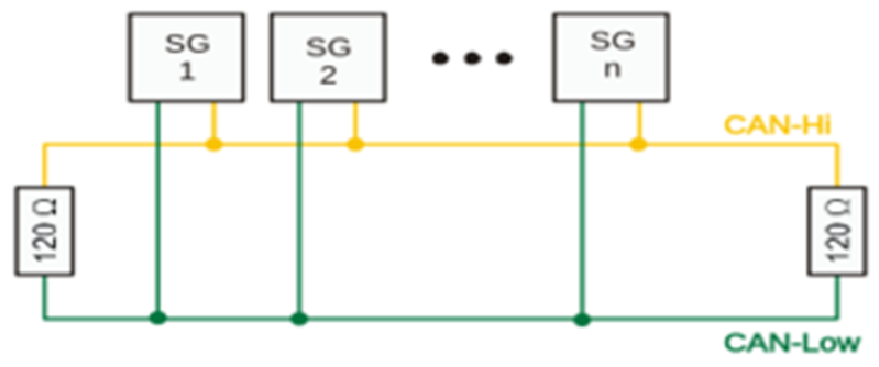
As applications may require many nodes (SG), which are not predetermined, both conventional CAN A/B bus and CAN FD bus require proper termination (120-ohm resistor at each end of the bus) to operate properly. A new feature to NAI’s CAN FD module is the ability to assign termination to desired channels in code rather than requiring a physical resistor to be attached.
Continuous Background Built-in Test (BIT)/Diagnostic Capability
BIT is performed in the background continuously within the FPGA. Each channel is checked periodically at 80MHz for correct operation. Any failure triggers an interrupt if enabled, with the results available in the status registers. The testing is transparent to the user and has no effect on the operation of the CB8.
REGISTER DESCRIPTIONS
The register descriptions provide the register name, Register Offset, Type, Data Range, Read or Write information, Default Value, a description of the function and, in most cases, a data table.
Receive Registers
The registers listed are associated with data that is received on the CAN Bus channels
Receive FIFO Buffer Data |
|
Function: |
Stores received messages. |
Type: |
unsigned binary word (32-bit) |
Data Range: |
0x0000 0000 to 0xFFFF FFFF |
Read/Write: |
W-H, R-A |
Operational Settings: |
N/A |
Default: |
0 |
CAN Frame as it is to be read off the FIFO - The FIFO contains 32-bit values where the top 8 bits are reserved for flags. The payload is “packed” where up to 3 x 8-bit values are stuffed into 1 x 32-bit read from the FIFO (upper 8 bits are always reserved for flags)
Description |
Bits Read |
Meaningful Bits |
NOTES |
Msg ID - Lower 16 |
32 |
Lower 16 (0x0000FFFF) |
Lower and Upper make up 29 Bit Identifier |
Msg ID - Upper 16 |
32 |
Upper 16 (0x0000FFFF) |
|
Timestamp - Lower 16 |
32 |
Lower 16 (0x0000FFFF) |
Lower and Upper Timestamp |
Timestamp - Upper 16 |
32 |
Upper 16 (0x0000FFFF) |
|
Msg/Payload Length |
32 |
1 Byte (0x000000FF) |
Length of Msg (payload count) |
Payload Data is “Packed” - lower 24 bits make up 3 x 8 bits of data. Top 8 bits are reserved for flags. |
|||
Data[0], Data[1], Data[2] |
32 |
||
Data[0] |
X |
1st Byte (0x000000FF) |
1st Byte is Data[0] |
Data[1] |
X |
2nd Byte (0x0000FF00) |
2nd Byte is Data[1] |
Data[2] |
X |
3rd Byte (0x00FF0000) |
3rd Byte is Data[2] |
If msg length indicates more data to read…another 32 bits would be read from the FIFO |
|||
Data[3], Data[4], Data[5] |
32 |
||
Data[3] |
X |
1st Byte (0x000000FF) |
1st Byte is Data[3] |
Data[4] |
X |
2nd Byte (0x0000FF00) |
2nd Byte is Data[4] |
Data[5] |
X |
3rd Byte (0x00FF0000) |
3rd Byte is Data[5] |
This continues until Data[MsgLen -1] |
Receive FIFO Word Count |
|
Function: |
Contains the number of 32-bit words in the Receive FIFO buffer. |
Type: |
unsigned integer word |
Data Range: |
0 to 1048576 (0 to 0x0010 0000) |
Read/Write: |
R |
Operational Settings: |
N/A |
Default: |
0 |
Receive FIFO Frame Count |
|
Function: |
Contains the number of frames in the Receive FIFO buffer. |
Type: |
unsigned integer word |
Data Range: |
0 to 409 (0 to 0x0000 0199) (Minimum CAN frame will be 5 entries on the FIFO) |
Read/Write: |
R |
Operational Settings: |
Each minimum CAN frame is 5; 32-bit words that get placed on the FIFO. Maximum frame count is thus 2048 (0x0000 0800) / 5 = 409 (0x0000 0199). |
Default: |
0 |
Transmit Registers
The registers listed are associated with data that is transmitted on the CAN Bus channels.
Transmit FIFO Buffer Data |
|
Function: |
Transmits messages in FIFO |
Type: |
unsigned binary word (32-bit) |
Data Range: |
0x0000 0000 to 0xFFFF FFFF |
Read/Write: |
W-H, R-A |
Operational Settings: |
N/A |
Default: |
0 |
CAN Frame as it is to be read off the FIFO - The FIFO contains 32-bit values where the top 8 bits are reserved for flags. The payload is “packed” where up to 3 x 8-bit values are stuffed into 1 x 32-bit read from the FIFO (upper 8 bits are always reserved for flags)
Description |
Bits Read |
Meaningful Bits |
NOTES |
Protocol |
32 |
0xFF00000F |
Valid Protocol values are 0 and 1. Flag for Start of message is 0x80000000 |
Msg ID - Lower 16 |
32 |
Lower 16 (0x0000FFFF) |
Lower and Upper make up 29 Bit Identifier |
Msg ID - Upper 16 |
32 |
Upper 16 (0x0000FFFF) |
|
Extended ID |
32 |
0x0000000F |
Mode A = 0 |
Msg/Payload Length |
32 |
1 Byte (0x000000FF) |
Length of Msg (payload count). If zero payload, the End of Message Flag (0x10000000) will be set |
Payload Data is “Packed” - lower 24 bits make up 3 x 8 bits of data. Top 8 bits are reserved for flags. |
End of Message Flag (0x10000000) will be set on the last payload data value only. |
||
Data[0], Data[1], Data[2] |
32 |
||
Data[0] |
X |
1st Byte (0x000000FF) |
1st Byte is Data[0] |
Data[1] |
X |
2nd Byte (0x0000FF00) |
2nd Byte is Data[1] |
Data[2] |
X |
3rd Byte (0x00FF0000) |
3rd Byte is Data[2] |
If msg length indicates more data to read…another 32 bits would be read from the FIFO |
|||
Data[3], Data[4], Data[5] |
32 |
||
Data[3] |
X |
1st Byte (0x000000FF) |
1st Byte is Data[3] |
Data[4] |
X |
2nd Byte (0x0000FF00) |
2nd Byte is Data[4] |
Data[5] |
X |
3rd Byte (0x00FF0000) |
3rd Byte is Data[5] |
This continues until Data[MsgLen -1] |
Transmit FIFO Word Count |
|
Function: |
Contains the number of 32-bit words in the Transmit FIFO register. |
Type: |
unsigned integer word |
Data Range: |
0 to 1048576 (0 to 0x0010 0000) |
Read/Write: |
R |
Operational Settings: |
N/A |
Default: |
0 |
Transmit FIFO Frame Count |
|
Function: |
Contains the number of frames in the Transmit FIFO register. |
Type: |
unsigned integer word |
Data Range: |
0 to 409 (0 to 0x0000 0199) (Minimum CAN frame will be 5 entries on the FIFO) |
Read/Write: |
R |
Operational Settings: |
Each minimum CAN frame is 5; 32-bit words that get placed on the FIFO. Maximum frame count is thus 2048 (0x0000 0800) / 5 = 409 (0x0000 0199). |
Default: |
0 |
Command Registers
The registers listed are associated with functionality which enables Tx and Rx FIFO to be dedicated to sending and receiving CAN FD messages.
BareMetal Capabilities Register |
|
Function: |
Determines if the revision of BM can use Command FIFO, response registers and can set the device sample point. |
Type: |
unsigned integer word |
Data Range: |
0 to 0x5 |
Read/Write: |
R/W |
Operational Settings: |
See table below |
Default: |
0 |
D31 |
D30 |
D29 |
D28 |
D27 |
D26 |
D25 |
D24 |
D23 |
D22 |
D21 |
D20 |
D19 |
D18 |
D17 |
D16 |
0 |
0 |
0 |
0 |
0 |
0 |
0 |
0 |
0 |
0 |
0 |
0 |
0 |
0 |
0 |
0 |
D15 |
D14 |
D13 |
D12 |
D11 |
D10 |
D9 |
D8 |
D7 |
D6 |
D5 |
D4 |
D3 |
D2 |
D1 |
D0 |
0 |
0 |
0 |
0 |
0 |
0 |
0 |
0 |
0 |
0 |
0 |
0 |
0 |
D |
D |
D |
Bit |
Description |
D0 |
Cmd FIFO in Use: if set to 1, Cmd FIFO is available and can be used to send parameters to the BareMetal. |
D1 |
Sample Point: If set to 1, the BareMetal is capable of setting the sample point to the desired value. |
D2 |
Response Registers: If set to 1, the BareMetal is using these registers to return data instead of the Rx FIFO. |
D4:D31 |
<RESERVED FOR FUTURE> |
Command FIFO Buffer Data |
|
Function: |
Transmits BareMetal parameters in FIFO |
Type: |
unsigned binary word (32-bit) |
Data Range: |
0 to 0xFFFF FFFF |
Read/Write: |
W-H, R-A |
Operational Settings: |
N/A |
Default: |
0 |
Command FIFO Word Count |
|
Function: |
Contains the number of words in the Command FIFO register. |
Type: |
unsigned integer word |
Data Range: |
0 to 32 (0 to 0x0000 0020) |
Read/Write: |
R |
Operational Settings: |
N/A |
Default: |
0 |
Control Registers
The register specified in this section provides the ability to control the operation for each CAN Bus channel.
Control
The control register has been implemented to act solely as a “request for action” register. Bits can be set to a 1 to request various actions or capabilities. When the action or capability is acted upon by the CAN firmware, these request bits will be set back to 0.
Control |
|
Function: |
Provides flags for controlling transmit and receive activity. |
Type: |
binary word (32-bit) |
Data Range: |
0x0000 0000 to 0x87FF BFF3 |
Read/Write: |
R/W |
Operational Settings: |
See descriptions that follow. |
Default: |
0 (disabled) |
D31 |
D30 |
D29 |
D28 |
D27 |
D26 |
D25 |
D24 |
D23 |
D22 |
D21 |
D20 |
D19 |
D18 |
D17 |
D16 |
D |
0 |
0 |
0 |
0 |
D |
D |
D |
D |
D |
D |
D |
D |
D |
D |
D |
D15 |
D14 |
D13 |
D12 |
D11 |
D10 |
D9 |
D8 |
D7 |
D6 |
D5 |
D4 |
D3 |
D2 |
D1 |
D0 |
D |
0 |
D |
D |
D |
D |
D |
D |
D |
D |
D |
D |
0 |
0 |
D |
D |
Bit |
Description |
D0 |
Request Enable Tx: Enables any messages found in the Tx FIFO to be placed on the bus from the current channel. |
D1 |
Request Disable Tx: Stops any messages currently in the Tx FIFO from being put on the bus from the current channel. |
D2 |
<RESERVED FOR FUTURE> |
D3 |
<RESERVED FOR FUTURE> |
D4: |
Request Set Level Dominant: This is for Debug purposes only and forces channel bus signal to a constant dominant value. |
D5 |
Request Set Level Recessive: This is for Debug purposes only and forces channel bus signal to a constant recessive value. |
D6 |
Request Enable Termination: Internal termination will be enabled for the current channel. |
D7 |
Request Disable Termination: Internal termination will be disabled for the current channel. |
D8 |
Request Base Rate Change: Desired base rate enumerated type value needs to be assigned to the lower 16 bits of the datarate-baserate register. Valid values include 0 (1Mb), 1 (500K), 3 (250K), 7 (125K) and 9 (83.33K) |
D9 |
Request Data Rate Change: Desired data rate enumerated type value needs to be assigned to the upper 16 bits of the datarate-baserate register. Valid values include 6 (4Mb), 7 (3Mb), 8 (2Mb) and 9 (1Mb). NOTE: Data rate of 3 Mb is not recommended as it has been found to be unreliable. |
D10 |
Request reset of Tx FIFO: Clears the entire Tx FIFO |
D11 |
Request reset of Rx FIFO: Clears the entire Rx FIFO |
D12 |
Request reset of Drop Count: Resets the counter that keeps track of how many messages were dropped due to FIFO already being full. |
D13 |
Request reset of Command FIFO: Clears the entire Command FIFO. |
D14: |
<RESERVED FOR FUTURE> |
D15 |
Request Reset Channel. Expected for next release: Reset Channel will reset both the Tx, Rx and Cmd FIFOs, disable Tx enable, Clear any Last Error Code, zero out Tx/Rx error counter and drop count registers and reset entire set of response registers. Reset Channel also retains the configured baud rate so the baud rates that were configured prior to the reset will be reassigned after the reset completes back to the same baud rates. |
D16: |
Request Config Sequencer: Allows caller to configure a given sequencer (schedule). Configuration data is expected to be placed on the Tx FIFO in the following order: (1) Requested Config Sequencer Cmd ID so we know the data following this is the data needed to configure a new sequencer/schedule. |
D17 |
Request Start Sequencer/Scheduler: This will start all configured sequencers/schedules |
D18 |
Request Stop Sequencer/Scheduler: This will stop all configured sequencers/schedules |
D19 |
Set Sample Point: Provides flexibility to assign various sample point values (75% or 80%) to the CAN FD core since it is important that all CAN FD devices use the same sample point to detect bit rate switching (BRS). |
D20 |
Request Enable Filters: Enables all filters configured for the current channel. |
D21 |
Request Disable Filters: Disables all filters configured for the current channel. |
D22 |
Request Set Filter: Allows caller to configure a filter (A total of 8 filters can be configured indexed from 0 - 7). Filter configuration data is expected to be placed on the Cmd FIFO in the following order: (1) Set Filter Cmd ID: so we know the data following this is the data needed to configure a new filter. |
D23 |
Request Get Filter: Retrieves desired filter data. The following is expected to be on the Cmd FIFO when this control bit value is detected being set: (1) Get Filter Cmd ID: so we know the data following this is the data needed to get desired filter information. NOTE: The response data will be made available in the set of response registers. |
D24 |
Request Set Filter Mask: The following data is expected to be on the Cmd FIFO in order to configure the desired Filter Mask. The Filter Mask is used on incoming messages that are received and on the corresponding Filter configuration data that was set where Filter Index = Mask Index. After applying the mask to both, the corresponding bits are compared and if both sides match, the data is received else it is rejected. (1) Set Filter Mask Cmd ID: so we know the data following this is the data needed to configure a new filter mask. |
D25 |
Request Get Filter Mask: Retrieves desired filter mask configuration data. The following is expected to be on the Cmd FIFO when this control bit value is detected being set: (1) Get Filter Mask Cmd ID: so we know the data following this is the data needed to get desired filter mask information. NOTE: The response data will be made available in the set of response registers for the given channel. |
D26 |
Request Remove Filter: Removes desired filter from the filter configuration. The following is expected to be on the FIFO when this control bit is detected being set: (1) Remove Filter Cmd ID: so we know the data following this is the data needed to remove desired filter information. |
D27 |
<RESERVED FOR FUTURE> |
D28 |
<RESERVED FOR FUTURE> |
D29 |
<RESERVED FOR FUTURE> |
D30 |
<RESERVED FOR FUTURE> |
D31 |
Config edit flag when set to a 1 it indicates end-user is currently editing the control register and we should not yet act upon set values. If 0, all bits in the control register will be evaluated and acted upon. |
Data Rate/Base Rate |
|
Function: |
Indicates the current rate (speed) at which data is being transmitted on the CAN network. User applications should always specifically configure the Baud Rates for each active channel and not rely on the default values set within the BareMetal. |
Type: |
unsigned binary word (32-bit) |
Data Range: |
Lower 16 bits range is 0 - 3…Upper 16 bits range is from 6 - 9. |
Read/Write: |
R/W |
Operational Settings: |
Upper 16 bits dedicated to data rate enumerated type value; Lower 16 bits dedicated to base rate enumerated type value. |
Default: |
0 for Base Rate; |
Data Rate (CAN FD only) |
|||||||||||||||
D31 |
D30 |
D29 |
D28 |
D27 |
D26 |
D25 |
D24 |
D23 |
D22 |
D21 |
D20 |
D19 |
D18 |
D17 |
D16 |
D |
D |
D |
D |
D |
D |
D |
D |
D |
D |
D |
D |
D |
D |
D |
D |
Base Rate |
|||||||||||||||
D15 |
D14 |
D13 |
D12 |
D11 |
D10 |
D9 |
D8 |
D7 |
D6 |
D5 |
D4 |
D3 |
D2 |
D1 |
D0 |
D |
D |
D |
D |
D |
D |
D |
D |
D |
D |
D |
D |
D |
D |
D |
D |
Valid values for Base Rate currently include: |
|
0: |
1Mb (1000K) Base Baud |
1: |
500K Base Baud |
3: |
250K Base Baud |
7: |
125K Base Baud |
9: |
83.33 Base Baud |
Valid values for Data Rate currently include: |
|
6: |
4Mb (4000K) Data Baud |
7: |
3Mb (3000K) Data Baud |
8: |
2Mb (2000K) Data Baud |
9: |
1Mb (1000K) Data Baud |
|
Note
|
Data rate of 3 Mb is not recommended as it has been found to be unreliable. |
Sample Point |
|
Function: |
Indicates the sample point to be used. Different 3rd party vendor equipment may use different sample points. This register provides some flexibility to the NAI CAN FD functionality. |
Type: |
unsigned binary word (32-bit) |
Data Range: |
0 (75%) to 0x0000 0001 (80%) |
Read/Write: |
R/W |
Operational Settings: |
The sample point can be set to 75% or 80% depending on which value works best for the CAN FD operational environment |
Default: |
0x0000 0001 (80%) |
RxMaxWorkTimeMS |
|
Function: |
Defines length of time user will wait to perform receiving of CAN FD messages before processing control is returned to all other processing. |
Type: |
unsigned binary word (32-bit) |
Data Range: |
0 to 0xFFFF FFFF |
Read/Write: |
R/W |
Operational Settings: |
1000ms / 0ms |
Default: |
1000ms (if Enhanced Last Error Code capabilities bit is 0); |
TxMaxWorkTimeMS |
|
Function: |
Defines length of time user will wait to perform transmitting of CAN FD messages before processing control is returned to all other processing. |
Type: |
unsigned binary word (32-bit) |
Data Range: |
0 to 0xFFFF FFFF |
Read/Write: |
R/W |
Operational Settings: |
1000ms / 0ms |
Default: |
1000ms (if Enhanced Last Error Code capabilities bit is 0); |
Transmit Enable State |
|
Function: |
Reflects the state of Transmit Enable. |
Type: |
unsigned binary word (32-bit) |
Data Range: |
0 to 0x1 |
Read/Write: |
R/W |
Operational Settings: |
See below. |
Default: |
0 |
D31 |
D30 |
D29 |
D28 |
D27 |
D26 |
D25 |
D24 |
D23 |
D22 |
D21 |
D20 |
D19 |
D18 |
D17 |
D16 |
0 |
0 |
0 |
0 |
0 |
0 |
0 |
0 |
0 |
0 |
0 |
0 |
0 |
0 |
0 |
0 |
D15 |
D14 |
D13 |
D12 |
D11 |
D10 |
D9 |
D8 |
D7 |
D6 |
D5 |
D4 |
D3 |
D2 |
D1 |
D0 |
0 |
0 |
0 |
0 |
0 |
0 |
0 |
0 |
0 |
0 |
0 |
0 |
0 |
0 |
0 |
D |
Bit |
Description |
D0 |
Tx Enabled when bit reflects a 1 |
Message Status/Monitoring Registers
The registers specified in this section provide status and monitoring information on about the CAN Bus messages.
FIFO Status |
|
Function: |
Describes current FIFO Status. |
Type: |
unsigned binary word (32-bit) |
Data Range: |
NA |
Read/Write: |
R |
Operational Settings: |
See table below. |
Bit |
Description |
Configurable? |
D0 |
Rx FIFO EMPTY: When set to 1: Rx FIFO is empty. |
No |
D1 |
Rx FIFO ALMOST EMPTY: When set to 1: Rx FIFO is at 20% capacity. |
No |
D2 |
Rx FIFO ALMOST FULL: When set to 1: Rx FIFO is at 80% capacity. |
No |
D3 |
Rx FIFO FULL: When set to 1: Rx FIFO is full. |
No |
D4 |
Tx FIFO EMPTY: When set to 1: Tx FIFO is empty. |
No |
D5 |
Tx FIFO ALMOST EMPTY: When set to 1: Tx FIFO is at 20% capacity. |
No |
D6 |
Tx FIFO ALMOST FULL: When set to 1: Tx FIFO is at 80% capacity. |
No |
D7 |
Tx FIFO FULL: When set to 1: Tx FIFO is full. |
No |
Last Error Code (LEC) |
|
Function: |
Stores the value of the last detected error. |
Type: |
signed binary word (32-bit) if compatibility bit D3 from BareMetal Compatibilities Registers is 0 (Non-Enhanced Error Code) |
Data Range: |
0 = success; negative value = failure |
Read/Write: |
R/W (to allow register to be cleared) |
Operational Settings: |
The last error code to be received on a channel. |
Default: |
0 |
D31 |
D30 |
D29 |
D28 |
D27 |
D26 |
D25 |
D24 |
D23 |
D22 |
D21 |
D20 |
D19 |
D18 |
D17 |
D16 |
D |
D |
D |
D |
D |
D |
D |
D |
D |
D |
D |
D |
D |
D |
D |
D |
D15 |
D14 |
D13 |
D12 |
D11 |
D10 |
D9 |
D8 |
D7 |
D6 |
D5 |
D4 |
D3 |
D2 |
D1 |
D0 |
D |
D |
D |
D |
D |
D |
D |
D |
D |
D |
D |
D |
D |
D |
D |
D |
Common Error Values |
|
-50: |
INVALID_DEVICE_NUMBER |
-65: |
INVALID PARAMETER |
-1009: |
MESSAGE NOT DETECTED |
Full List of Error Values when Enhanced Error Code: |
|
(HEX) |
Error Description |
0x0001 |
NAI_BUS ERROR |
0x0002 |
NAI_SEQUENCER_START_ERROR |
0x0003 |
NAI_SEQUENCER_STOP_ERROR |
0x0004 |
NAI_SEQUENCER_INDEX_ERROR |
0x0005 |
NAI_SET_DEVICE_MODE_ERROR |
0x0006 |
NAI_BAUD_RATE_CHANGE_ERROR |
0x0007 |
NAI_ENABLE_FILTERS_ERROR |
0x0008 |
NAI_DISABLE_FILTERS_ERROR |
0x0009 |
NAI_MISSING_END_OF_MSG_ERROR |
0x000A |
NAI_INSUFFICIENT_DATA_ERROR |
0x000B |
NAI_EXPECTED_CMD_NOT_FOUND_ERROR |
0x000C |
NAI_INIT_DEVICE_ERROR |
0x000D |
NAI_OPEN_DEVICE_ERROR |
0x000E |
NAI_NO_ROOM_ON_RX_FIFO_ERROR |
0x0010 |
NAI_FILTER_INDEX_ERROR |
0x0011 |
NAI_SET_FILTER_ERROR |
0x0012 |
NAI_GET_FILTER_ERROR |
0x0013 |
NAI_SET_FILTER_MASK_ERROR |
0x0014 |
NAI_GET_FILTER_MASK_ERROR |
0x0015 |
NAI_REMOVE_FILTER_ERROR |
0x0020 |
NAI_IP_GENERAL_API_ERROR |
0x0021 |
NAI_IP_TX_FIFO_FULL |
0x0022 |
NAI_IP_RX_FIFO_FULL |
Drop Count |
|
Function: |
Every time a received message is unable to be placed onto the Rx FIFO because the FIFO is full, the message will be dropped, and this register’s value will be incremented by 1. This Drop count can be reset by sending the request to reset the drop count command via the control register (see data bit 12 (D12) of the control register description). |
Type: |
unsigned binary word (32-bit) |
Data Range: |
0 - 0xFFFF FFFF |
Read/Write: |
R/W |
Operational Settings: |
Drop Count |
Default: |
0 |
D31 |
D30 |
D29 |
D28 |
D27 |
D26 |
D25 |
D24 |
D23 |
D22 |
D21 |
D20 |
D19 |
D18 |
D17 |
D16 |
D |
D |
D |
D |
D |
D |
D |
D |
D |
D |
D |
D |
D |
D |
D |
D |
D15 |
D14 |
D13 |
D12 |
D11 |
D10 |
D9 |
D8 |
D7 |
D6 |
D5 |
D4 |
D3 |
D2 |
D1 |
D0 |
D |
D |
D |
D |
D |
D |
D |
D |
D |
D |
D |
D |
D |
D |
D |
D |
Status and Interrupt Registers
The registers may be set for any or all channels and will latch if a transition is detected on a channel or channels. Each channel(s) will remain latched until the channel is cleared. Multiple channels may be cleared simultaneously, if desired. Each channel bit in the register is polled for a read status. Any subsequent channel(s) transition, if detected, will propagate through to be read (rolling-latch).
Once the status register has been read, the act of writing a 1 back to the applicable status register to any specific bit (channel) location (bit-mapped per channel), will “clear” the bit (set the bit to 0) if the actual interruptible event condition has cleared. If the interruptible condition “event” is still persistent while clearing, this may retrigger the interrupt.
There is a corresponding Interrupt Enable and vector associated with each “Latched” Status. Each status type may be “polled” (at any time) or is “interruptible” when interrupts are enabled and the associated Interrupt Service Routine (ISR) vectors are programmed accordingly. When programmed for “interruptible” status, interrupts are typically generated and flagged with the programmed vector available as data. The host or single board computer (SBC) typically services the interrupt by a general or specific ISR, which reads the (typically) unique programmed vector (identifier of which status generated the interrupt), reads the associated status register to determine which channel in the status register was “flagged” and then “clears” the status register. This essentially resets the interrupt mechanism, which is now ready to be triggered by the next status register detected event “flag”. “Latched Status” will trigger on either “sense on edge” or “sense on level” based on the settings of the associated Set Edge/Level Interrupt register. Sense on “edge” requires a change from low to high state to trigger the status detection, while sense on “level” is independent of the previous state. Unless otherwise specified, all status or fault indications are bit set per channel.
BIT Status
There are four registers associated with the BIT Status: Dynamic, Latched, Interrupt Enable, and Set Edge/Level Interrupt
BIT Dynamic Status |
|||||||||||||||
BIT Latched Status |
|||||||||||||||
BIT Interrupt Enable |
|||||||||||||||
BIT Set Edge/Level Interrupt |
|||||||||||||||
D31 |
D30 |
D29 |
D28 |
D27 |
D26 |
D25 |
D24 |
D23 |
D22 |
D21 |
D20 |
D19 |
D18 |
D17 |
D16 |
0 |
0 |
0 |
0 |
0 |
0 |
0 |
0 |
0 |
0 |
0 |
0 |
0 |
0 |
0 |
0 |
D15 |
D14 |
D13 |
D12 |
D11 |
D10 |
D9 |
D8 |
D7 |
D6 |
D5 |
D4 |
D3 |
D2 |
D1 |
D0 |
0 |
0 |
0 |
0 |
0 |
0 |
0 |
0 |
Ch8 |
Ch7 |
Ch6 |
Ch5 |
Ch4 |
Ch3 |
Ch2 |
Ch1 |
BIT Dynamic Status |
|
Function: |
Indicates current condition of Built-In Test (BIT). |
Type: |
unsigned binary word (32-bit) |
Data Range: |
0 to 0x0000 00FF |
Read/Write: |
R |
Operational Settings: |
NA |
Default: |
0 |
BIT Latched Status |
|
Function: |
Sets and maintains the status of running Built-In Test (BIT), until cleared. |
Type: |
unsigned binary word (32-bit) |
Read/Write: |
R/W |
Operational Settings: |
Write 1 to clear register. |
Default: |
0 |
BIT Interrupt Enable |
|
Function: |
Sets the corresponding channel to enable an interrupt for whenever BIT fails for that channel. |
Type: |
unsigned binary word (32-bit) |
Data Range: |
0 to 0x0000 00FF |
Read/Write: |
R/W |
Operational Settings: |
When enabled, an interrupt will be generated whenever BIT fails for the channel. Each channel may be set for a different condition. |
Default: |
0 |
BIT Set Edge/Level Interrupt |
|
Function: |
Determines whether Interrupt Enable register will generate an interrupt for “sense on edge” or “sense on level” event detection. |
Type: |
unsigned binary word (32-bit) |
Data Range: |
0 to 0x0000 00FF |
Read/Write: |
R/W |
Operational Settings: |
Write a 1 to sense on level and a 0 to sense on edge. |
Default: |
Sense on edge (0) |
Reset BIT |
|
Function: |
Set the bit corresponding to the channel you want to clear. |
Type: |
unsigned binary word (32-bit) |
Data Range: |
0 - 0x0000 00FF |
Read/Write: |
R/W |
Initialized Value: |
0 |
Operational Settings: |
Set bit to 1 for channel you want to clear. Bit is self-clearing. |
D31 |
D30 |
D29 |
D28 |
D27 |
D26 |
D25 |
D24 |
D23 |
D22 |
D21 |
D20 |
D19 |
D18 |
D17 |
D16 |
0 |
0 |
0 |
0 |
0 |
0 |
0 |
0 |
0 |
0 |
0 |
0 |
0 |
0 |
0 |
0 |
D15 |
D14 |
D13 |
D12 |
D11 |
D10 |
D9 |
D8 |
D7 |
D6 |
D5 |
D4 |
D3 |
D2 |
D1 |
D0 |
0 |
0 |
0 |
0 |
0 |
0 |
0 |
0 |
Ch8 |
Ch7 |
Ch6 |
Ch5 |
Ch4 |
Ch3 |
Ch2 |
Ch1 |
New Data Available Status
There are four registers associated with the New Data Available Status: Dynamic, Latched, Interrupt Enable, and Set Edge/Level Interrupt.
New Data Available Dynamic Status |
|||||||||||||||
New Data Available Latched Status |
|||||||||||||||
New Data Available Interrupt Enable |
|||||||||||||||
New Data Available Set Edge/Level Interrupt |
|||||||||||||||
D31 |
D30 |
D29 |
D28 |
D27 |
D26 |
D25 |
D24 |
D23 |
D22 |
D21 |
D20 |
D19 |
D18 |
D17 |
D16 |
0 |
0 |
0 |
0 |
0 |
0 |
0 |
0 |
0 |
0 |
0 |
0 |
0 |
0 |
0 |
0 |
D15 |
D14 |
D13 |
D12 |
D11 |
D10 |
D9 |
D8 |
D7 |
D6 |
D5 |
D4 |
D3 |
D2 |
D1 |
D0 |
0 |
0 |
0 |
0 |
0 |
0 |
0 |
0 |
Ch8 |
Ch7 |
Ch6 |
Ch5 |
Ch4 |
Ch3 |
Ch2 |
Ch1 |
New Data Available Dynamic Status |
|
Function: |
Indicates current condition of received data in Receive FIFO register. |
Type: |
binary word (32-bit) |
Data Range: |
0 to 0x0000 00FF |
Read/Write: |
R |
Operational Settings: |
NA |
Default: |
0 |
New Data Available Latched Status |
|
Function: |
Sets and maintains the status of received data in Receive FIFO register, until cleared. |
Type: |
binary word (32-bit) |
Data Range: |
0 to 0x00FF |
Read/Write: |
R/W |
Operational Settings: |
Write 1 to clear register. |
Default: |
0 |
New Data Available Interrupt Enable |
|
Function: |
Sets the corresponding channel to enable an interrupt for when CAN data is received. |
Type: |
binary word (32-bit) |
Data Range: |
0 to 0x00FF |
Read/Write: |
R/W |
Operational Settings: |
When enabled, an interrupt will be generated for each time CAN data is received in the receive FIFO. Only one interrupt vector exists for all channels. Caller must interrogate the interrupt status register to determine which channel caused the interrupt. |
Default: |
0 |
New Data Available Set Edge/Level Interrupt |
|
Function: |
Determines whether Interrupt Enable register will generate an interrupt for “sense on edge” or “sense on level” event detection. |
Type: |
binary word (32-bit) |
Data Range: |
0 to 0x00FF |
Read/Write: |
R/W |
Operational Settings: |
Write a 1 to sense on level and a 0 to sense on edge. |
Default: |
Sense on edge (0) |
FIFO Status
There are four registers associated with the FIFO Status: Dynamic, Latched, Interrupt Enable, and Set Edge/Level Interrupt.
FIFO Dynamic Status |
|||||||||||||||
FIFO Latched Status |
|||||||||||||||
FIFO Interrupt Enable |
|||||||||||||||
FIFO Set Edge/Level Interrupt |
|||||||||||||||
D31 |
D30 |
D29 |
D28 |
D27 |
D26 |
D25 |
D24 |
D23 |
D22 |
D21 |
D20 |
D19 |
D18 |
D17 |
D16 |
0 |
0 |
0 |
0 |
0 |
0 |
0 |
0 |
0 |
0 |
0 |
0 |
0 |
0 |
0 |
0 |
D15 |
D14 |
D13 |
D12 |
D11 |
D10 |
D9 |
D8 |
D7 |
D6 |
D5 |
D4 |
D3 |
D2 |
D1 |
D0 |
0 |
0 |
0 |
0 |
0 |
0 |
0 |
0 |
D |
D |
D |
D |
D |
D |
D |
D |
Bit |
Description |
Configurable? |
D0 |
Rx FIFO EMPTY: When set to 1: Rx FIFO is empty. |
No |
D1 |
Rx FIFO ALMOST EMPTY: When set to 1: Rx FIFO is at 20% capacity. |
No |
D2 |
Rx FIFO ALMOST FULL: When set to 1: Rx FIFO is at 80% capacity. |
No |
D3 |
Rx FIFO FULL: When set to 1: Rx FIFO is full. |
No |
D4 |
Tx FIFO EMPTY: When set to 1: Tx FIFO is empty. |
No |
D5 |
Tx FIFO ALMOST EMPTY: When set to 1: Tx FIFO is at 20% capacity. |
No |
D6 |
Tx FIFO ALMOST FULL: When set to 1: Tx FIFO is at 80% capacity. |
No |
D7 |
Tx FIFO FULL: When set to 1: Tx FIFO is full. |
No |
FIFO Dynamic Status |
|
Function: |
Checks the corresponding bit for a channel’s FIFO Status. The FIFO Dynamic Status register indicates the current condition of the FIFO buffer. |
Type: |
binary word (32-bit) |
Data Range: |
0 to 0x0000 00FF |
Read/Write: |
R |
Initialized Value: |
0 |
Operational Settings: |
D0-D7 is used to show the different conditions of the buffer. |
FIFO Latched Status |
|
Function: |
Checks the corresponding bit for a channel’s FIFO Status. The FIFO Latched Status register maintains the last condition of the FIFO buffer, until cleared. |
Type: |
binary word (32-bit) |
Data Range: |
0 to 0x0000 00FF |
Read/Write: |
R/W |
Initialized Value: |
0 |
Operational Settings: |
D0-D7 is used to show the different conditions of the buffer. Write a 1 to this register to clear status. |
FIFO Interrupt Enable |
|
Function: |
Interrupts may be enabled based on D0-D7 FIFO Status. |
Type: |
unsigned binary word (32-bit) |
Data Range: |
0x0000 0000 to 0x0000 00FF |
Read/Write: |
R/W |
Initialized Value: |
0 (Not Enabled) |
Notes:
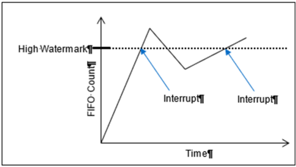
-
Shown below is an example of interrupts generated for the High Watermark. As shown, the interrupt is generated as the FIFO Word Count crosses the High Watermark. The interrupt will not be generated a second time until the count goes below the watermark and then above it again.
FIFO Set Edge/Level Interrupt |
|
Function: |
When the FIFO Status Interrupt Enable register is enabled, this register determines whether the interrupt will be generated for either “sense on edge” or “sense on level” event detection. |
Read/Write: |
R/W |
Initialized Value: |
0 |
Operational Settings: |
Write a 1 to sense on level and a 0 to sense on edge. |
Function Register Map
KEY
Input |
Output |
| RECEIVE REGISTERS | |||||
|---|---|---|---|---|---|
NOTE: Base Address - 0x4000 0000 |
|||||
OFFSET |
REGISTER NAME |
ACCESS |
OFFSET |
REGISTER NAME |
ACCESS |
0x1004 |
Receive FIFO Buffer Data Ch 1 |
R-H, W-A |
0x1008 |
Receive FIFO Word Count Ch 1 |
R |
0x1084 |
Receive FIFO Buffer Data Ch 2 |
R-H, W-A |
0x1088 |
Receive FIFO Word Count Ch 2 |
R |
0x1104 |
Receive FIFO Buffer Data Ch 3 |
R-H, W-A |
0x1108 |
Receive FIFO Word Count Ch 3 |
R |
0x1184 |
Receive FIFO Buffer Data Ch 4 |
R-H, W-A |
0x1188 |
Receive FIFO Word Count Ch 4 |
R |
0x1204 |
Receive FIFO Buffer Data Ch 5 |
R-H, W-A |
0x1208 |
Receive FIFO Word Count Ch 5 |
R |
0x1284 |
Receive FIFO Buffer Data Ch 6 |
R-H, W-A |
0x1288 |
Receive FIFO Word Count Ch 6 |
R |
0x1304 |
Receive FIFO Buffer Data Ch 7 |
R-H, W-A |
0x1308 |
Receive FIFO Word Count Ch 7 |
R |
0x1384 |
Receive FIFO Buffer Data Ch 8 |
R-H, W-A |
0x1388 |
Receive FIFO Word Count Ch 8 |
R |
NOTE: For Receive FIFO Buffer Data, 'H' is 'Host; 'A' is 'ARM'. |
|||||
0x100C |
Receive FIFO Frame Count Ch 1 |
R |
|||
0x108C |
Receive FIFO Frame Count Ch 2 |
R |
|||
0x110C |
Receive FIFO Frame Count Ch 3 |
R |
|||
0x118C |
Receive FIFO Frame Count Ch 4 |
R |
|||
0x120C |
Receive FIFO Frame Count Ch 5 |
R |
|||
0x128C |
Receive FIFO Frame Count Ch 6 |
R |
|||
0x130C |
Receive FIFO Frame Count Ch 7 |
R |
|||
0x138C |
Receive FIFO Frame Count Ch 8 |
R |
|||
TRANSMIT REGISTERS |
|||||
NOTE: Base Address - 0x4000 0000 |
|||||
OFFSET |
REGISTER NAME |
ACCESS |
OFFSET |
REGISTER NAME |
ACCESS |
0x1010 |
Transmit FIFO Buffer Data Ch 1 |
W-H, R-A |
0x1014 |
Transmit FIFO Word Count Ch 1 |
R |
0x1090 |
Transmit FIFO Buffer Data Ch 2 |
W-H, R-A |
0x1094 |
Transmit FIFO Word Count Ch 2 |
R |
0x1110 |
Transmit FIFO Buffer Data Ch 3 |
W-H, R-A |
0x1114 |
Transmit FIFO Word Count Ch 3 |
R |
0x1190 |
Transmit FIFO Buffer Data Ch 4 |
W-H, R-A |
0x1194 |
Transmit FIFO Word Count Ch 4 |
R |
0x1210 |
Transmit FIFO Buffer Data Ch 5 |
W-H, R-A |
0x1214 |
Transmit FIFO Word Count Ch 5 |
R |
0x1290 |
Transmit FIFO Buffer Data Ch 6 |
W-H, R-A |
0x1294 |
Transmit FIFO Word Count Ch 6 |
R |
0x1310 |
Transmit FIFO Buffer Data Ch 7 |
W-H, R-A |
0x1314 |
Transmit FIFO Word Count Ch 7 |
R |
0x1390 |
Transmit FIFO Buffer Data Ch 8 |
W-H, R-A |
0x1394 |
Transmit FIFO Word Count Ch 8 |
R |
NOTE: For Transmit FIFO Buffer Data, 'H' is 'Host; 'A' is 'ARM'. |
|||||
0x1018 |
Transmit FIFO Frame Count Ch 1 |
R |
|||
0x1098 |
Transmit FIFO Frame Count Ch 2 |
R |
|||
0x1118 |
Transmit FIFO Frame Count Ch 3 |
R |
|||
0x1198 |
Transmit FIFO Frame Count Ch 4 |
R |
|||
0x1218 |
Transmit FIFO Frame Count Ch 5 |
R |
|||
0x1298 |
Transmit FIFO Frame Count Ch 6 |
R |
|||
0x1318 |
Transmit FIFO Frame Count Ch 7 |
R |
|||
0x1398 |
Transmit FIFO Frame Count Ch 8 |
R |
|||
COMMAND REGISTERS |
|||||
NOTE: Base Address - 0x4000 0000 |
|||||
OFFSET |
REGISTER NAME |
ACCESS |
OFFSET |
REGISTER NAME |
ACCESS |
0x1400 |
BM Capabilities Register |
R/W |
|||
0x1028 |
Command FIFO Buffer Data Ch 1 |
W-H, R-A |
0x102C |
Command FIFO Word Count Ch 1 |
R |
0x10A8 |
Command FIFO Buffer Data Ch 2 |
W-H, R-A |
0x10AC |
Command FIFO Word Count Ch 2 |
R |
0x1128 |
Command FIFO Buffer Data Ch 3 |
W-H, R-A |
0x112C |
Command FIFO Word Count Ch 3 |
R |
0x11A8 |
Command FIFO Buffer Data Ch 4 |
W-H, R-A |
0x11AC |
Command FIFO Word Count Ch 4 |
R |
0x1228 |
Command FIFO Buffer Data Ch 5 |
W-H, R-A |
0x122C |
Command FIFO Word Count Ch 5 |
R |
0x12A8 |
Command FIFO Buffer Data Ch 6 |
W-H, R-A |
0x12AC |
Command FIFO Word Count Ch 6 |
R |
0x1328 |
Command FIFO Buffer Data Ch 7 |
W-H, R-A |
0x132C |
Command FIFO Word Count Ch 7 |
R |
0x13A8 |
Command FIFO Buffer Data Ch 8 |
W-H, R-A |
0x13AC |
Command FIFO Word Count Ch 8 |
R |
NOTE: For Command FIFO Buffer Data, 'H' is 'Host; 'A' is 'ARM'. |
|||||
CONTROL REGISTERS |
|||||
NOTE: Base Address - 0x4000 0000 |
|||||
OFFSET |
REGISTER NAME |
ACCESS |
OFFSET |
REGISTER NAME |
ACCESS |
0x1000 |
Control Ch 1 |
R/W |
0x101C |
Data Rate/Base Rate Ch 1 |
R/W |
0x1080 |
Control Ch 2 |
R/W |
0x109C |
Data Rate/Base Rate Ch 2 |
R/W |
0x1100 |
Control Ch 3 |
R/W |
0x111C |
Data Rate/Base Rate Ch 3 |
R/W |
0x1180 |
Control Ch 4 |
R/W |
0x119C |
Data Rate/Base Rate Ch 4 |
R/W |
0x1200 |
Control Ch 5 |
R/W |
0x121C |
Data Rate/Base Rate Ch 5 |
R/W |
0x1280 |
Control Ch 6 |
R/W |
0x129C |
Data Rate/Base Rate Ch 6 |
R/W |
0x1300 |
Control Ch 7 |
R/W |
0x131C |
Data Rate/Base Rate Ch 7 |
R/W |
0x1380 |
Control Ch 8 |
R/W |
0x139C |
Data Rate/Base Rate Ch 8 |
R/W |
0x1020 |
Sample Point Ch 1 |
R/W |
0x1060 |
RxMaxWorkMS Ch 1 |
R/W |
0x10A0 |
Sample Point Ch 2 |
R/W |
0x10E0 |
RxMaxWorkMS Ch 2 |
R/W |
0x1120 |
Sample Point Ch 3 |
R/W |
0x1160 |
RxMaxWorkMS Ch 3 |
R/W |
0x11A0 |
Sample Point Ch 4 |
R/W |
0x11E0 |
RxMaxWorkMS Ch 4 |
R/W |
0x1220 |
Sample Point Ch 5 |
R/W |
0x1260 |
RxMaxWorkMS Ch 5 |
R/W |
0x12A0 |
Sample Point Ch 6 |
R/W |
0x12E0 |
RxMaxWorkMS Ch 6 |
R/W |
0x1320 |
Sample Point Ch 7 |
R/W |
0x1360 |
RxMaxWorkMS Ch 7 |
R/W |
0x13A0 |
Sample Point Ch 8 |
R/W |
0x13E0 |
RxMaxWorkMS Ch 8 |
R/W |
0x1064 |
TxMaxWorkMS Ch 1 |
R/W |
0x1068 |
Tx Enable State Ch 1 |
R |
0x10E4 |
TxMaxWorkMS Ch 2 |
R/W |
0x10E8 |
Tx Enable State Ch 2 |
R |
0x1164 |
TxMaxWorkMS Ch 3 |
R/W |
0x1168 |
Tx Enable State Ch 3 |
R |
0x11E4 |
TxMaxWorkMS Ch 4 |
R/W |
0x11E8 |
Tx Enable State Ch 4 |
R |
0x1264 |
TxMaxWorkMS Ch 5 |
R/W |
0x1268 |
Tx Enable State Ch 5 |
R |
0x12E4 |
TxMaxWorkMS Ch 6 |
R/W |
0x12E8 |
Tx Enable State Ch 6 |
R |
0x1364 |
TxMaxWorkMS Ch 7 |
R/W |
0x1368 |
Tx Enable State Ch 7 |
R |
0x13E4 |
TxMaxWorkMS Ch 8 |
R/W |
0x13E8 |
Tx Enable State Ch 8 |
R |
MESSAGE STATUS/MONITOR REGISTERS |
|||||
NOTE: Base Address - 0x4000 0000 |
|||||
OFFSET |
REGISTER NAME |
ACCESS |
OFFSET |
REGISTER NAME |
ACCESS |
0x104C |
FIFO Status Ch 1 |
R |
|||
0x10CC |
FIFO Status Ch 2 |
R |
|||
0x114C |
FIFO Status Ch 3 |
R |
|||
0x11CC |
FIFO Status Ch 4 |
R |
|||
0x124C |
FIFO Status Ch 5 |
R |
|||
0x12CC |
FIFO Status Ch 6 |
R |
|||
0x134C |
FIFO Status Ch 7 |
R |
|||
0x13CC |
FIFO Status Ch 8 |
R |
|||
0x1024 |
Last Error Code Ch 1 |
R/W |
0x1050 |
Drop Count Ch 1 |
R/W |
0x10A4 |
Last Error Code Ch 2 |
R/W |
0x10D0 |
Drop Count Ch 2 |
R/W |
0x1124 |
Last Error Code Ch 3 |
R/W |
0x1150 |
Drop Count Ch 3 |
R/W |
0x11A4 |
Last Error Code Ch 4 |
R/W |
0x11D0 |
Drop Count Ch 4 |
R/W |
0x1224 |
Last Error Code Ch 5 |
R/W |
0x1250 |
Drop Count Ch 5 |
R/W |
0x12A4 |
Last Error Code Ch 6 |
R/W |
0x12D0 |
Drop Count Ch 6 |
R/W |
0x1324 |
Last Error Code Ch 7 |
R/W |
0x1350 |
Drop Count Ch 7 |
R/W |
0x13A4 |
Last Error Code Ch 8 |
R/W |
0x13D0 |
Drop Count Ch 8 |
R/W |
BIT REGISTER |
|||||
NOTE: Base Address - 0x4000 0000 |
|||||
*When an event is detected, the bit associated with the event is set in this register and will remain set until the user clears the event bit. Clearing the bit requires writing a 1 back to the specific bit that was set when read (i.e. write-1-to-clear, writing a '1' to a bit set to '1' will set the bit to '0'). |
|||||
OFFSET |
REGISTER NAME |
ACCESS |
OFFSET |
REGISTER NAME |
ACCESS |
0x0800 |
BIT Dynamic Status |
R |
|||
0x0804 |
BIT Latched Status* |
R/W |
|||
0x0808 |
BIT Interrupt Enable |
R/W |
|||
0x080C |
BIT Set Edge/Level Interrupt |
R/W |
|||
0x02B8 |
Reset BIT |
R/W |
|||
FIFO STATUS REGISTERS |
|||||
NOTE: Base Address - 0x4000 0000 |
|||||
*When an event is detected, the bit associated with the event is set in this register and will remain set until the user clears the event bit. Clearing the bit requires writing a 1 back to the specific bit that was set when read (i.e. write-1-to-clear, writing a '1' to a bit set to '1' will set the bit to '0'). |
|||||
OFFSET |
REGISTER NAME |
ACCESS |
OFFSET |
REGISTER NAME |
ACCESS |
0x0810 |
Dynamic Status Ch 1 |
R |
0x0820 |
Dynamic Status Ch 2 |
R |
0x0814 |
Latched Status Ch 1* |
R/W |
0x0824 |
Latched Status Ch 2* |
R/W |
0x0818 |
Interrupt Enable Ch 1 |
R/W |
0x0828 |
Interrupt Enable Ch 2 |
R/W |
0x081C |
Set Edge/Level Interrupt Ch 1 |
R/W |
0x082C |
Set Edge/Level Interrupt Ch 2 |
R/W |
0x0830 |
Dynamic Status Ch 3 |
R |
0x0840 |
Dynamic Status Ch 4 |
R |
0x0834 |
Latched Status Ch 3* |
R/W |
0x0844 |
Latched Status Ch 4* |
R/W |
0x0838 |
Interrupt Enable Ch 3 |
R/W |
0x0848 |
Interrupt Enable Ch 4 |
R/W |
0x083C |
Set Edge/Level Interrupt Ch 3 |
R/W |
0x084C |
Set Edge/Level Interrupt Ch 4 |
R/W |
0x0850 |
Dynamic Status Ch 5 |
R |
0x0860 |
Dynamic Status Ch 6 |
R |
0x0854 |
Latched Status Ch 5* |
R/W |
0x0864 |
Latched Status Ch 6* |
R/W |
0x0858 |
Interrupt Enable Ch 5 |
R/W |
0x0868 |
Interrupt Enable Ch 6 |
R/W |
0x085C |
Set Edge/Level Interrupt Ch 5 |
R/W |
0x086C |
Set Edge/Level Interrupt Ch 6 |
R/W |
0x0870 |
Dynamic Status Ch 7 |
R |
0x0880 |
Dynamic Status Ch 8 |
R |
0x0874 |
Latched Status Ch 7* |
R/W |
0x0884 |
Latched Status Ch 8* |
R/W |
0x0878 |
Interrupt Enable Ch 7 |
R/W |
0x0888 |
Interrupt Enable Ch 8 |
R/W |
0x087C |
Set Edge/Level Interrupt Ch 7 |
R/W |
0x088C |
Set Edge/Level Interrupt Ch 8 |
R/W |
NEW DATA AVAILABLE REGISTER |
|||||
NOTE: Base Address - 0x4000 0000 |
|||||
OFFSET |
REGISTER NAME |
ACCESS |
OFFSET |
REGISTER NAME |
ACCESS |
0x0890 |
Dynamic Status Ch 1-8 |
R |
|||
0x0894 |
Latched Status Ch 1-8* |
R/W |
|||
0x0898 |
Interrupt Enable Ch 1-8 |
R/W |
|||
0x089C |
Set Edge/Level Interrupt Ch 1-8 |
R/W |
|||
RESPONSE REGISTERS |
|||||
When data other than CAN messages needs to be returned from the CAN module, the data to be returned is placed in a series of Response Registers. Each channel has its own series of Response Registers that can be used. The BareMetal logic will fill these registers and update the Response Count so the consumer can determine how many of the Response Registers need to be read. |
|||||
NOTE: Base Address - 0x4000 0000 |
|||||
OFFSET |
REGISTER NAME |
ACCESS |
OFFSET |
REGISTER NAME |
ACCESS |
0x1500 |
Response Count Ch 1 |
R |
0x1580 |
Response Count Ch 2 |
R |
0x1504 |
Response Data Ch 1 |
R |
0x1584 |
Response Data Ch 2 |
R |
0x1508 |
Response Data Ch 1 |
R |
0x1588 |
Response Data Ch 2 |
R |
0x150C |
Response Data Ch 1 |
R |
0x158C |
Response Data Ch 2 |
R |
… |
… |
||||
0x157C |
Response Data Ch 1 |
R |
0x15FC |
Response Data Ch 2 |
R |
0x1600 |
Response Count Ch 3 |
R |
0x1680 |
Response Count Ch 4 |
R |
0x1604 |
Response Data Ch 3 |
R |
0x1684 |
Response Data Ch 4 |
R |
0x1608 |
Response Data Ch 3 |
R |
0x1688 |
Response Data Ch 4 |
R |
0x160C |
Response Data Ch 3 |
R |
0x168C |
Response Data Ch 4 |
R |
… |
… |
||||
0x167C |
Response Data Ch 3 |
R |
0x16FC |
Response Data Ch 4 |
R |
0x1700 |
Response Count Ch 5 |
R |
0x1780 |
Response Count Ch 6 |
R |
0x1704 |
Response Data Ch 5 |
R |
0x1784 |
Response Data Ch 6 |
R |
0x1708 |
Response Data Ch 5 |
R |
0x1788 |
Response Data Ch 6 |
R |
0x170C |
Response Data Ch 5 |
R |
0x178C |
Response Data Ch 6 |
R |
… |
… |
||||
0x177C |
Response Data Ch 5 |
R |
0x17FC |
Response Data Ch 6 |
R |
0x1800 |
Response Count Ch 7 |
R |
0x1880 |
Response Count Ch 8 |
R |
0x1804 |
Response Data Ch 7 |
R |
0x1884 |
Response Data Ch 8 |
R |
0x1808 |
Response Data Ch 7 |
R |
0x1888 |
Response Data Ch 8 |
R |
0x180C |
Response Data Ch 7 |
R |
0x188C |
Response Data Ch 8 |
R |
… |
… |
||||
0x187C |
Response Data Ch 7 |
R |
0x18FC |
Response Data Ch 8 |
R |
APPENDIX: PIN-OUT DETAILS
Pin-out details (for reference) are shown below, with respect to DATAIO. Additional information on pin-outs can be found in the Motherboard Operational Manuals.
Module Signal |
44-Pin I/O |
50-Pin I/O (Mod Slot 1-J3) |
50-Pin I/O (Mod Slot 2-J4) |
50-Pin I/O (Mod Slot 3-J3) |
50-Pin I/O (Mod Slot 3-J4) |
CAN 2.0 A/B, |
DATIO1 |
2 |
10 |
1 |
2 |
CANH-CH1 |
|
DATIO2 |
24 |
35 |
26 |
27 |
CANL-CH1 |
|
DATIO3 |
3 |
11 |
2 |
3 |
CANH-CH2 |
|
DATIO4 |
25 |
36 |
27 |
28 |
CANL-CH2 |
|
DATIO5 |
5 |
13 |
4 |
5 |
ISO_GND_CH2 |
|
DATIO6 |
27 |
38 |
29 |
30 |
ISO_GND_CH1 |
|
DATIO7 |
7 |
14 |
5 |
6 |
CANH-CH3 |
|
DATIO8 |
29 |
39 |
30 |
31 |
CANL-CH3 |
|
DATIO9 |
8 |
15 |
6 |
7 |
CANH-CH4 |
|
DATIO10 |
30 |
40 |
31 |
32 |
CANL-CH4 |
|
DATIO11 |
10 |
17 |
8 |
9 |
ISO_GND_CH3 |
|
DATIO12 |
32 |
42 |
33 |
34 |
ISO_GND_CH4 |
|
DATIO13 |
12 |
18 |
9 |
17 |
CANH-CH5 |
|
DATIO14 |
34 |
43 |
34 |
42 |
CANL-CH5 |
|
DATIO15 |
13 |
19 |
10 |
18 |
CANH-CH6 |
|
DATIO16 |
35 |
44 |
35 |
43 |
CANL-CH6 |
|
DATIO17 |
15 |
44 |
35 |
43 |
ISO_GND_CH6 |
|
DATIO18 |
37 |
46 |
37 |
45 |
ISO_GND_CH5 |
|
DATIO19 |
17 |
22 |
13 |
21 |
CANH-CH7 |
|
DATIO20 |
39 |
47 |
38 |
46 |
CANL-CH7 |
|
DATIO21 |
18 |
23 |
14 |
22 |
CANH-CH8 |
|
DATIO22 |
40 |
48 |
39 |
47 |
CANL-CH8 |
|
DATIO23 |
20 |
25 |
16 |
24 |
ISO_GND_CH8 |
|
DATIO24 |
42 |
50 |
41 |
49 |
ISO_GND_CH7 |
|
DATIO25 |
4 |
12 |
3 |
4 |
||
DATIO26 |
26 |
37 |
28 |
29 |
||
DATIO27 |
9 |
16 |
7 |
8 |
||
DATIO28 |
31 |
41 |
32 |
33 |
||
DATIO29 |
14 |
20 |
11 |
19 |
||
DATIO30 |
36 |
45 |
36 |
44 |
||
DATIO31 |
19 |
24 |
15 |
23 |
||
DATIO32 |
41 |
49 |
40 |
48 |
||
DATIO33 |
6 |
|||||
DATIO34 |
28 |
|||||
DATIO35 |
11 |
|||||
DATIO36 |
33 |
|||||
DATIO37 |
16 |
|||||
DATIO38 |
38 |
|||||
DATIO39 |
21 |
|||||
DATIO40 |
43 |
|||||
N/A |
DOCS.NAII REVISIONS
Revision Date |
Description |
2026-03-10 |
Initial release of CB8 manual. |
STATUS AND INTERRUPTS
Edit this on GitLab
Status registers indicate the detection of faults or events. The status registers can be channel bit-mapped or event bit-mapped. An example of a channel bit-mapped register is the BIT status register, and an example of an event bit-mapped register is the FIFO status register.
For those status registers that allow interrupts to be generated upon the detection of the fault or the event, there are four registers associated with each status: Dynamic, Latched, Interrupt Enabled, and Set Edge/Level Interrupt.
Dynamic Status: The Dynamic Status register indicates the current condition of the fault or the event. If the fault or the event is momentary, the contents in this register will be clear when the fault or the event goes away. The Dynamic Status register can be polled, however, if the fault or the event is sporadic, it is possible for the indication of the fault or the event to be missed.
Latched Status: The Latched Status register indicates whether the fault or the event has occurred and keeps the state until it is cleared by the user. Reading the Latched Status register is a better alternative to polling the Dynamic Status register because the contents of this register will not clear until the user commands to clear the specific bit(s) associated with the fault or the event in the Latched Status register. Once the status register has been read, the act of writing a 1 back to the applicable status register to any specific bit (channel/event) location will “clear” the bit (set the bit to 0). When clearing the channel/event bits, it is strongly recommended to write back the same bit pattern as read from the Latched Status register. For example, if the channel bit-mapped Latched Status register contains the value 0x0000 0005, which indicates fault/event detection on channel 1 and 3, write the value 0x0000 0005 to the Latched Status register to clear the fault/event status for channel 1 and 3. Writing a “1” to other channels that are not set (example 0x0000 000F) may result in incorrectly “clearing” incoming faults/events for those channels (example, channel 2 and 4).
Interrupt Enable: If interrupts are preferred upon the detection of a fault or an event, enable the specific channel/event interrupt in the Interrupt Enable register. The bits in Interrupt Enable register map to the same bits in the Latched Status register. When a fault or event occurs, an interrupt will be fired. Subsequent interrupts will not trigger until the application acknowledges the fired interrupt by clearing the associated channel/event bit in the Latched Status register. If the interruptible condition is still persistent after clearing the bit, this may retrigger the interrupt depending on the Edge/Level setting.
Set Edge/Level Interrupt: When interrupts are enabled, the condition on retriggering the interrupt after the Latch Register is “cleared” can be specified as “edge” triggered or “level” triggered. Note, the Edge/Level Trigger also affects how the Latched Register value is adjusted after it is “cleared” (see below).
-
Edge triggered: An interrupt will be retriggered when the Latched Status register change from low (0) to high (1) state. Uses for edge-triggered interrupts would include transition detections (Low-to-High transitions, High-to-Low transitions) or fault detections. After “clearing” an interrupt, another interrupt will not occur until the next transition or the re-occurrence of the fault again.
-
Level triggered: An interrupt will be generated when the Latched Status register remains at the high (1) state. Level-triggered interrupts are used to indicate that something needs attention.
Interrupt Vector and Steering
When interrupts are enabled, the interrupt vector associated with the specific interrupt can be programmed with a unique number/identifier defined by the user such that it can be utilized in the Interrupt Service Routine (ISR) to identify the type of interrupt. When an interrupt occurs, the contents of the Interrupt Vector registers is reported as part of the interrupt mechanism. In addition to specifying the interrupt vector, the interrupt can be directed (“steered”) to the native bus or to the application running on the onboard ARM processor.
Interrupt Trigger Types
In most applications, limiting the number of interrupts generated is preferred as interrupts are costly, thus choosing the correct Edge/Level interrupt trigger to use is important.
Example 1: Fault detection
This example illustrates interrupt considerations when detecting a fault like an “open” on a line. When an “open” is detected, the system will receive an interrupt. If the “open” on the line is persistent and the trigger is set to “edge”, upon “clearing” the interrupt, the system will not regenerate another interrupt. If, instead, the trigger is set to “level”, upon “clearing” the interrupt, the system will re-generate another interrupt. Thus, in this case, it will be better to set the trigger type to “edge”.
Example 2: Threshold detection
This example illustrates interrupt considerations when detecting an event like reaching or exceeding the “high watermark” threshold value. In a communication device, when the number of elements received in the FIFO reaches the high-watermark threshold, an interrupt will be generated. Normally, the application would read the count of the number of elements in the FIFO and read this number of elements from the FIFO. After reading the FIFO data, the application would “clear” the interrupt. If the trigger type is set to “edge”, another interrupt will be generated only if the number of elements in FIFO goes below the “high watermark” after the “clearing” the interrupt and then fills up to reach the “high watermark” threshold value. Since receiving communication data is inherently asynchronous, it is possible that data can continue to fill the FIFO as the application is pulling data off the FIFO. If, at the time the interrupt is “cleared”, the number of elements in the FIFO is at or above the “high watermark”, no interrupts will be generated. In this case, it will be better to set the trigger type to “level”, as the purpose here is to make sure that the FIFO is serviced when the number of elements exceeds the high watermark threshold value. Thus, upon “clearing” the interrupt, if the number of elements in the FIFO is at or above the “high watermark” threshold value, another interrupt will be generated indicating that the FIFO needs to be serviced.
Dynamic and Latched Status Registers Examples
The examples in this section illustrate the differences in behavior of the Dynamic Status and Latched Status registers as well as the differences in behavior of Edge/Level Trigger when the Latched Status register is cleared.
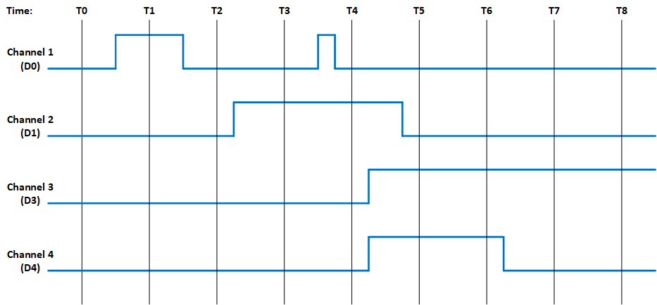
Figure 1. Example of Module’s Channel-Mapped Dynamic and Latched Status States
| No Clearing of Latched Status | Clearing of Latched Status (Edge-Triggered) | Clearing of Latched Status(Level-Triggered) | ||||
|---|---|---|---|---|---|---|
Time |
Dynamic Status |
Latched Status |
Action |
Latched Status |
Action |
Latched |
T0 |
0x0 |
0x0 |
Read Latched Register |
0x0 |
Read Latched Register |
0x0 |
T1 |
0x1 |
0x1 |
Read Latched Register |
0x1 |
0x1 |
|
T1 |
0x1 |
0x1 |
Write 0x1 to Latched Register |
Write 0x1 to Latched Register |
||
T1 |
0x1 |
0x1 |
0x0 |
0x1 |
||
T2 |
0x0 |
0x1 |
Read Latched Register |
0x0 |
Read Latched Register |
0x1 |
T2 |
0x0 |
0x1 |
Read Latched Register |
0x0 |
Write 0x1 to Latched Register |
|
T2 |
0x0 |
0x1 |
Read Latched Register |
0x0 |
0x0 |
|
T3 |
0x2 |
0x3 |
Read Latched Register |
0x2 |
Read Latched Register |
0x2 |
T3 |
0x2 |
0x3 |
Write 0x2 to Latched Register |
Write 0x2 to Latched Register |
||
T3 |
0x2 |
0x3 |
0x0 |
0x2 |
||
T4 |
0x2 |
0x3 |
Read Latched Register |
0x1 |
Read Latched Register |
0x3 |
T4 |
0x2 |
0x3 |
Write 0x1 to Latched Register |
Write 0x3 to Latched Register |
||
T4 |
0x2 |
0x3 |
0x0 |
0x2 |
||
T5 |
0xC |
0xF |
Read Latched Register |
0xC |
Read Latched Register |
0xE |
T5 |
0xC |
0xF |
Write 0xC to Latched Register |
Write 0xE to Latched Register |
||
T5 |
0xC |
0xF |
0x0 |
0xC |
||
T6 |
0xC |
0xF |
Read Latched Register |
0x0 |
Read Latched |
0xC |
T6 |
0xC |
0xF |
Read Latched Register |
0x0 |
Write 0xC to Latched Register |
|
T6 |
0xC |
0xF |
Read Latched Register |
0x0 |
0xC |
|
T7 |
0x4 |
0xF |
Read Latched Register |
0x0 |
Read Latched Register |
0xC |
T7 |
0x4 |
0xF |
Read Latched Register |
0x0 |
Write 0xC to Latched Register |
|
T7 |
0x4 |
0xF |
Read Latched Register |
0x0 |
0x4 |
|
T8 |
0x4 |
0xF |
Read Latched Register |
0x0 |
Read Latched Register |
0x4 |
Interrupt Examples
The examples in this section illustrate the interrupt behavior with Edge/Level Trigger.
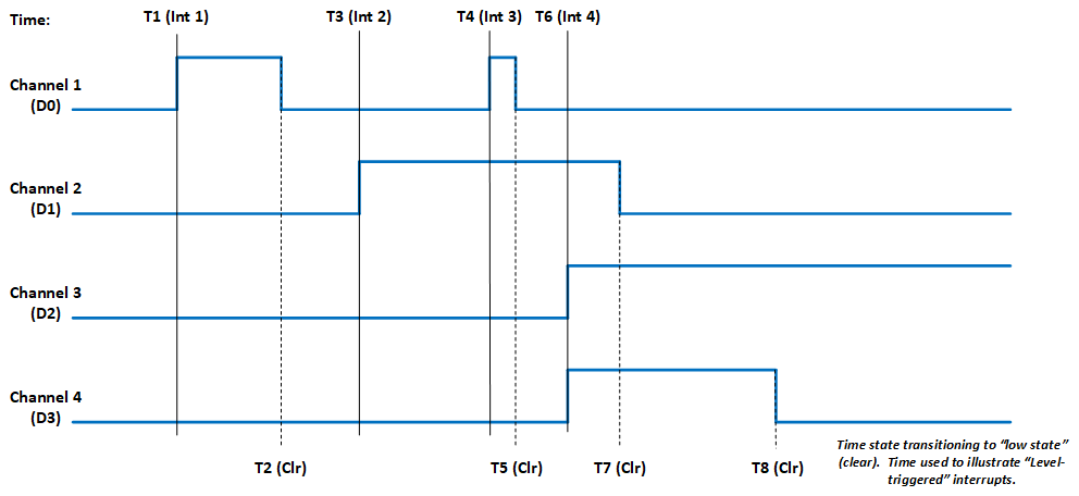
Figure 2. Illustration of Latched Status State for Module with 4-Channels with Interrupt Enabled
Time |
Latched Status (Edge-Triggered - Clear Multi-Channel) |
Latched Status (Edge-Triggered - Clear Single Channel) |
Latched Status (Level-Triggered - Clear Multi-Channel) |
|||
Action |
Latched |
Action |
Latched |
Action |
Latched |
|
T1 (Int 1) |
Interrupt Generated Read Latched Registers |
0x1 |
Interrupt Generated Read Latched Registers |
0x1 |
Interrupt Generated Read Latched Registers |
0x1 |
T1 (Int 1) |
Write 0x1 to Latched Register |
Write 0x1 to Latched Register |
Write 0x1 to Latched Register |
|||
T1 (Int 1) |
0x0 |
0x0 |
Interrupt re-triggers Note, interrupt re-triggers after each clear until T2. |
0x1 |
||
T3 (Int 2) |
Interrupt Generated Read Latched Registers |
0x2 |
Interrupt Generated Read Latched Registers |
0x2 |
Interrupt Generated Read Latched Registers |
0x2 |
T3 (Int 2) |
Write 0x2 to Latched Register |
Write 0x2 to Latched Register |
Write 0x2 to Latched Register |
|||
T3 (Int 2) |
0x0 |
0x0 |
Interrupt re-triggers Note, interrupt re-triggers after each clear until T7. |
0x2 |
||
T4 (Int 3) |
Interrupt Generated Read Latched Registers |
0x1 |
Interrupt Generated Read Latched Registers |
0x1 |
Interrupt Generated Read Latched Registers |
0x3 |
T4 (Int 3) |
Write 0x1 to Latched Register |
Write 0x1 to Latched Register |
Write 0x3 to Latched Register |
|||
T4 (Int 3) |
0x0 |
0x0 |
Interrupt re-triggers Note, interrupt re-triggers after each clear and 0x3 is reported in Latched Register until T5. |
0x3 |
||
T4 (Int 3) |
0x0 |
0x0 |
Interrupt re-triggers Note, interrupt re-triggers after each clear until T7. |
0x2 |
||
T6 (Int 4) |
Interrupt Generated Read Latched Registers |
0xC |
Interrupt Generated Read Latched Registers |
0xC |
Interrupt Generated Read Latched Registers |
0xE |
T6 (Int 4) |
Write 0xC to Latched Register |
Write 0x4 to Latched Register |
Write 0xE to Latched Register |
|||
T6 (Int 4) |
0x0 |
Interrupt re-triggers Write 0x8 to Latched Register |
0x8 |
Interrupt re-triggers Note, interrupt re-triggers after each clear and 0xE is reported in Latched Register until T7. |
0xE |
|
T6 (Int 4) |
0x0 |
0x0 |
Interrupt re-triggers Note, interrupt re-triggers after each clear and 0xC is reported in Latched Register until T8. |
0xC |
||
T6 (Int 4) |
0x0 |
0x0 |
Interrupt re-triggers Note, interrupt re-triggers after each clear and 0x4 is reported in Latched Register always. |
0x4 |
||
REVISION HISTORY
Motherboard Manual - Status and Interrupts Revision History |
||
Revision |
Revision Date |
Description |
C |
2021-11-30 |
C08896; Transition manual to docbuilder format - no technical info change. |
DOCS.NAII REVISIONS
Revision Date |
Description |
2026-03-02 |
Formatting updates to document; no technical changes. |
MODULE COMMON REGISTERS
Edit this on GitLab
The registers described in this document are common to all NAI Generation 5 modules.
Module Information Registers
The registers in this section provide module information such as firmware revisions, capabilities and unique serial number information.
FPGA Version Registers
The FPGA firmware version registers include registers that contain the Revision, Compile Timestamp, SerDes Revision, Template Revision and Zynq Block Revision information.
FPGA Revision |
|
Function: |
FPGA firmware revision |
Type: |
unsigned binary word (32-bit) |
Data Range: |
0x0000 0000 to 0xFFFF FFFF |
Read/Write: |
R |
Initialized Value: |
Value corresponding to the revision of the board’s FPGA |
Operational Settings: |
The upper 16-bits are the major revision and the lower 16-bits are the minor revision. |
D31 |
D30 |
D29 |
D28 |
D27 |
D26 |
D25 |
D24 |
D23 |
D22 |
D21 |
D20 |
D19 |
D18 |
D17 |
D16 |
Major Revision Number |
|||||||||||||||
D15 |
D14 |
D13 |
D12 |
D11 |
D10 |
D9 |
D8 |
D7 |
D6 |
D5 |
D4 |
D3 |
D2 |
D1 |
D0 |
Minor Revision Number |
|||||||||||||||
FPGA Compile Timestamp |
|
Function: |
Compile Timestamp for the FPGA firmware. |
Type: |
unsigned binary word (32-bit) |
Data Range: |
N/A |
Read/Write: |
R |
Initialized Value: |
Value corresponding to the compile timestamp of the board’s FPGA |
Operational Settings: |
The 32-bit value represents the Day, Month, Year, Hour, Minutes and Seconds as formatted in the table: |
D31 |
D30 |
D29 |
D28 |
D27 |
D26 |
D25 |
D24 |
D23 |
D22 |
D21 |
D20 |
D19 |
D18 |
D17 |
D16 |
day (5-bits) |
month (4-bits) |
year (6-bits) |
hr |
||||||||||||
D15 |
D14 |
D13 |
D12 |
D11 |
D10 |
D9 |
D8 |
D7 |
D6 |
D5 |
D4 |
D3 |
D2 |
D1 |
D0 |
hour (5-bits) |
minutes (6-bits) |
seconds (6-bits) |
|||||||||||||
FPGA SerDes Revision |
|
Function: |
FPGA SerDes revision |
Type: |
unsigned binary word (32-bit) |
Data Range: |
0x0000 0000 to 0xFFFF FFFF |
Read/Write: |
R |
Initialized Value: |
Value corresponding to the SerDes revision of the board’s FPGA |
Operational Settings: |
The upper 16-bits are the major revision, and the lower 16-bits are the minor revision. |
D31 |
D30 |
D29 |
D28 |
D27 |
D26 |
D25 |
D24 |
D23 |
D22 |
D21 |
D20 |
D19 |
D18 |
D17 |
D16 |
Major Revision Number |
|||||||||||||||
D15 |
D14 |
D13 |
D12 |
D11 |
D10 |
D9 |
D8 |
D7 |
D6 |
D5 |
D4 |
D3 |
D2 |
D1 |
D0 |
Minor Revision Number |
|||||||||||||||
FPGA Template Revision |
|
Function: |
FPGA Template revision |
Type: |
unsigned binary word (32-bit) |
Data Range: |
0x0000 0000 to 0xFFFF FFFF |
Read/Write: |
R |
Initialized Value: |
Value corresponding to the template revision of the board’s FPGA |
Operational Settings: |
The upper 16-bits are the major revision, and the lower 16-bits are the minor revision. |
D31 |
D30 |
D29 |
D28 |
D27 |
D26 |
D25 |
D24 |
D23 |
D22 |
D21 |
D20 |
D19 |
D18 |
D17 |
D16 |
Major Revision Number |
|||||||||||||||
D15 |
D14 |
D13 |
D12 |
D11 |
D10 |
D9 |
D8 |
D7 |
D6 |
D5 |
D4 |
D3 |
D2 |
D1 |
D0 |
Minor Revision Number |
|||||||||||||||
FPGA Zynq Block Revision |
|
Function: |
FPGA Zynq Block revision |
Type: |
unsigned binary word (32-bit) |
Data Range: |
0x0000 0000 to 0xFFFF FFFF |
Read/Write: |
R |
Initialized Value: |
Value corresponding to the Zynq block revision of the board’s FPGA |
Operational Settings: |
The upper 16-bits are the major revision, and the lower 16-bits are the minor revision. |
D31 |
D30 |
D29 |
D28 |
D27 |
D26 |
D25 |
D24 |
D23 |
D22 |
D21 |
D20 |
D19 |
D18 |
D17 |
D16 |
Major Revision Number |
|||||||||||||||
D15 |
D14 |
D13 |
D12 |
D11 |
D10 |
D9 |
D8 |
D7 |
D6 |
D5 |
D4 |
D3 |
D2 |
D1 |
D0 |
Minor Revision Number |
|||||||||||||||
Bare Metal Version Registers
The Bare Metal firmware version registers include registers that contain the Revision and Compile Time information.
Bare Metal Revision |
|
Function: |
Bare Metal firmware revision |
Type: |
unsigned binary word (32-bit) |
Data Range: |
0x0000 0000 to 0xFFFF FFFF |
Read/Write: |
R |
Initialized Value: |
Value corresponding to the revision of the board’s Bare Metal |
Operational Settings: |
The upper 16-bits are the major revision and the lower 16-bits are the minor revision. |
D31 |
D30 |
D29 |
D28 |
D27 |
D26 |
D25 |
D24 |
D23 |
D22 |
D21 |
D20 |
D19 |
D18 |
D17 |
D16 |
Major Revision Number |
|||||||||||||||
D15 |
D14 |
D13 |
D12 |
D11 |
D10 |
D9 |
D8 |
D7 |
D6 |
D5 |
D4 |
D3 |
D2 |
D1 |
D0 |
Minor Revision Number |
|||||||||||||||
Bare Metal Compile Time |
|
Function: |
Provides an ASCII representation of the Date/Time for the Bare Metal compile time. |
Type: |
24-character ASCII string - Six (6) unsigned binary word (32-bit) |
Data Range: |
N/A |
Read/Write: |
R |
Initialized Value: |
Value corresponding to the ASCII representation of the compile time of the board’s Bare Metal |
Operational Settings: |
The six 32-bit words provide an ASCII representation of the Date/Time. The hexadecimal values in the field below represent: May 17 2019 at 15:38:32 |
|
Note
|
little-endian order of ASCII values |
Word 1 (Ex. 0x2079614D) |
|||||||||||||||
D31 |
D30 |
D29 |
D28 |
D27 |
D26 |
D25 |
D24 |
D23 |
D22 |
D21 |
D20 |
D19 |
D18 |
D17 |
D16 |
Space (0x20) |
Month ('y' - 0x79) |
||||||||||||||
D15 |
D14 |
D13 |
D12 |
D11 |
D10 |
D9 |
D8 |
D7 |
D6 |
D5 |
D4 |
D3 |
D2 |
D1 |
D0 |
Month ('a' - 0x61) |
Month ('M' - 0x4D) |
||||||||||||||
Word 2 (Ex. 0x32203731) |
|||||||||||||||
D31 |
D30 |
D29 |
D28 |
D27 |
D26 |
D25 |
D24 |
D23 |
D22 |
D21 |
D20 |
D19 |
D18 |
D17 |
D16 |
Year ('2' - 0x32) |
Space (0x20) |
||||||||||||||
D15 |
D14 |
D13 |
D12 |
D11 |
D10 |
D9 |
D8 |
D7 |
D6 |
D5 |
D4 |
D3 |
D2 |
D1 |
D0 |
Day ('7' - 0x37) |
Day ('1' - 0x31) |
||||||||||||||
Word 3 (Ex. 0x20393130) |
|||||||||||||||
D31 |
D30 |
D29 |
D28 |
D27 |
D26 |
D25 |
D24 |
D23 |
D22 |
D21 |
D20 |
D19 |
D18 |
D17 |
D16 |
Space (0x20) |
Year ('9' - 0x39) |
||||||||||||||
D15 |
D14 |
D13 |
D12 |
D11 |
D10 |
D9 |
D8 |
D7 |
D6 |
D5 |
D4 |
D3 |
D2 |
D1 |
D0 |
Year ('1' - 0x31) |
Year ('0' - 0x30) |
||||||||||||||
Word 4 (Ex. 0x31207461) |
|||||||||||||||
D31 |
D30 |
D29 |
D28 |
D27 |
D26 |
D25 |
D24 |
D23 |
D22 |
D21 |
D20 |
D19 |
D18 |
D17 |
D16 |
Hour ('1' - 0x31) |
Space (0x20) |
||||||||||||||
D15 |
D14 |
D13 |
D12 |
D11 |
D10 |
D9 |
D8 |
D7 |
D6 |
D5 |
D4 |
D3 |
D2 |
D1 |
D0 |
'a' (0x74) |
't' (0x61) |
||||||||||||||
Word 5 (Ex. 0x38333A35) |
|||||||||||||||
D31 |
D30 |
D29 |
D28 |
D27 |
D26 |
D25 |
D24 |
D23 |
D22 |
D21 |
D20 |
D19 |
D18 |
D17 |
D16 |
Minute ('8' - 0x38) |
Minute ('3' - 0x33) |
||||||||||||||
D15 |
D14 |
D13 |
D12 |
D11 |
D10 |
D9 |
D8 |
D7 |
D6 |
D5 |
D4 |
D3 |
D2 |
D1 |
D0 |
':' (0x3A) |
Hour ('5' - 0x35) |
||||||||||||||
Word 6 (Ex. 0x0032333A) |
|||||||||||||||
D31 |
D30 |
D29 |
D28 |
D27 |
D26 |
D25 |
D24 |
D23 |
D22 |
D21 |
D20 |
D19 |
D18 |
D17 |
D16 |
NULL (0x00) |
Seconds ('2' - 0x32) |
||||||||||||||
D15 |
D14 |
D13 |
D12 |
D11 |
D10 |
D9 |
D8 |
D7 |
D6 |
D5 |
D4 |
D3 |
D2 |
D1 |
D0 |
Seconds ('3' - 0x33) |
':' (0x3A) |
||||||||||||||
FSBL Version Registers
The FSBL version registers include registers that contain the Revision and Compile Time information for the First Stage Boot Loader (FSBL).
FSBL Revision |
|
Function: |
FSBL firmware revision |
Type: |
unsigned binary word (32-bit) |
Data Range: |
0x0000 0000 to 0xFFFF FFFF |
Read/Write: |
R |
Initialized Value: |
Value corresponding to the revision of the board’s FSBL |
Operational Settings: |
The upper 16-bits are the major revision, and the lower 16-bits are the minor revision. |
D31 |
D30 |
D29 |
D28 |
D27 |
D26 |
D25 |
D24 |
D23 |
D22 |
D21 |
D20 |
D19 |
D18 |
D17 |
D16 |
Major Revision Number |
|||||||||||||||
D15 |
D14 |
D13 |
D12 |
D11 |
D10 |
D9 |
D8 |
D7 |
D6 |
D5 |
D4 |
D3 |
D2 |
D1 |
D0 |
Minor Revision Number |
|||||||||||||||
FSBL Compile Time |
|
Function: |
Provides an ASCII representation of the Date/Time for the FSBL compile time. |
Type: |
24-character ASCII string - Six (6) unsigned binary word (32-bit) |
Data Range: |
N/A |
Read/Write: |
R |
Initialized Value: |
Value corresponding to the ASCII representation of the Compile Time of the board’s FSBL |
Operational Settings: |
The six 32-bit words provide an ASCII representation of the Date/Time. |
The hexadecimal values in the field below represent: May 17 2019 at 15:38:32
|
Note
|
little-endian order of ASCII values |
Word 1 (Ex. 0x2079614D) |
|||||||||||||||
D31 |
D30 |
D29 |
D28 |
D27 |
D26 |
D25 |
D24 |
D23 |
D22 |
D21 |
D20 |
D19 |
D18 |
D17 |
D16 |
Space (0x20) |
Month ('y' - 0x79) |
||||||||||||||
D15 |
D14 |
D13 |
D12 |
D11 |
D10 |
D9 |
D8 |
D7 |
D6 |
D5 |
D4 |
D3 |
D2 |
D1 |
D0 |
Month ('a' - 0x61) |
Month ('M' - 0x4D) |
||||||||||||||
Word 2 (Ex. 0x32203731) |
|||||||||||||||
D31 |
D30 |
D29 |
D28 |
D27 |
D26 |
D25 |
D24 |
D23 |
D22 |
D21 |
D20 |
D19 |
D18 |
D17 |
D16 |
Year ('2' - 0x32) |
Space (0x20) |
||||||||||||||
D15 |
D14 |
D13 |
D12 |
D11 |
D10 |
D9 |
D8 |
D7 |
D6 |
D5 |
D4 |
D3 |
D2 |
D1 |
D0 |
Day ('7' - 0x37) |
Day ('1' - 0x31) |
||||||||||||||
Word 3 (Ex. 0x20393130) |
|||||||||||||||
D31 |
D30 |
D29 |
D28 |
D27 |
D26 |
D25 |
D24 |
D23 |
D22 |
D21 |
D20 |
D19 |
D18 |
D17 |
D16 |
Space (0x20) |
Year ('9' - 0x39) |
||||||||||||||
D15 |
D14 |
D13 |
D12 |
D11 |
D10 |
D9 |
D8 |
D7 |
D6 |
D5 |
D4 |
D3 |
D2 |
D1 |
D0 |
Year ('1' - 0x31) |
Year ('0' - 0x30) |
||||||||||||||
Word 4 (Ex. 0x31207461) |
|||||||||||||||
D31 |
D30 |
D29 |
D28 |
D27 |
D26 |
D25 |
D24 |
D23 |
D22 |
D21 |
D20 |
D19 |
D18 |
D17 |
D16 |
Hour ('1' - 0x31) |
Space (0x20) |
||||||||||||||
D15 |
D14 |
D13 |
D12 |
D11 |
D10 |
D9 |
D8 |
D7 |
D6 |
D5 |
D4 |
D3 |
D2 |
D1 |
D0 |
'a' (0x74) |
't' (0x61) |
||||||||||||||
Word 5 (Ex. 0x38333A35) |
|||||||||||||||
D31 |
D30 |
D29 |
D28 |
D27 |
D26 |
D25 |
D24 |
D23 |
D22 |
D21 |
D20 |
D19 |
D18 |
D17 |
D16 |
Minute ('8' - 0x38) |
Minute ('3' - 0x33) |
||||||||||||||
D15 |
D14 |
D13 |
D12 |
D11 |
D10 |
D9 |
D8 |
D7 |
D6 |
D5 |
D4 |
D3 |
D2 |
D1 |
D0 |
':' (0x3A) |
Hour ('5' - 0x35) |
||||||||||||||
Word 6 (Ex. 0x0032333A) |
|||||||||||||||
D31 |
D30 |
D29 |
D28 |
D27 |
D26 |
D25 |
D24 |
D23 |
D22 |
D21 |
D20 |
D19 |
D18 |
D17 |
D16 |
NULL (0x00) |
Seconds ('2' - 0x32) |
||||||||||||||
D15 |
D14 |
D13 |
D12 |
D11 |
D10 |
D9 |
D8 |
D7 |
D6 |
D5 |
D4 |
D3 |
D2 |
D1 |
D0 |
Seconds ('3' - 0x33) |
':' (0x3A) |
||||||||||||||
Module Serial Number Registers
The Module Serial Number registers include registers that contain the Serial Numbers for the Interface Board and the Functional Board of the module.
Interface Board Serial Number |
|
Function: |
Unique 128-bit identifier used to identify the interface board. |
Type: |
16-character ASCII string - Four (4) unsigned binary words (32-bit) |
Data Range: |
N/A |
Read/Write: |
R |
Initialized Value: |
Serial number of the interface board |
Operational Settings: |
This register is for information purposes only. |
Functional Board Serial Number |
|
Function: |
Unique 128-bit identifier used to identify the functional board. |
Type: |
16-character ASCII string - Four (4) unsigned binary words (32-bit) |
Data Range: |
N/A |
Read/Write: |
R |
Initialized Value: |
Serial number of the functional board |
Operational Settings: |
This register is for information purposes only. |
Module Capability |
|
Function: |
Provides indication for whether or not the module can support the following: SerDes block reads, SerDes FIFO block reads, SerDes packing (combining two 16-bit values into one 32-bit value) and floating point representation. The purpose for block access and packing is to improve the performance of accessing larger amounts of data over the SerDes interface. |
Type: |
unsigned binary word (32-bit) |
Data Range: |
0x0000 0000 to 0x0000 0107 |
Read/Write: |
R |
Initialized Value: |
0x0000 0107 |
Operational Settings: |
A “1” in the bit associated with the capability indicates that it is supported. |
D31 |
D30 |
D29 |
D28 |
D27 |
D26 |
D25 |
D24 |
D23 |
D22 |
D21 |
D20 |
D19 |
D18 |
D17 |
D16 |
0 |
0 |
0 |
0 |
0 |
0 |
0 |
0 |
0 |
0 |
0 |
0 |
0 |
0 |
0 |
0 |
D15 |
D14 |
D13 |
D12 |
D11 |
D10 |
D9 |
D8 |
D7 |
D6 |
D5 |
D4 |
D3 |
D2 |
D1 |
D0 |
0 |
0 |
0 |
0 |
0 |
0 |
0 |
Flt-Pt |
0 |
0 |
0 |
0 |
0 |
Pack |
FIFO Blk |
Blk |
Module Memory Map Revision |
|
Function: |
Module Memory Map revision |
Type: |
unsigned binary word (32-bit) |
Data Range: |
0x0000 0000 to 0xFFFF FFFF |
Read/Write: |
R |
Initialized Value: |
Value corresponding to the Module Memory Map Revision |
Operational Settings: |
The upper 16-bits are the major revision and the lower 16-bits are the minor revision. |
D31 |
D30 |
D29 |
D28 |
D27 |
D26 |
D25 |
D24 |
D23 |
D22 |
D21 |
D20 |
D19 |
D18 |
D17 |
D16 |
Major Revision Number |
|||||||||||||||
D15 |
D14 |
D13 |
D12 |
D11 |
D10 |
D9 |
D8 |
D7 |
D6 |
D5 |
D4 |
D3 |
D2 |
D1 |
D0 |
Minor Revision Number |
|||||||||||||||
Module Measurement Registers
The registers in this section provide module temperature measurement information.
Temperature Readings Registers
The temperature registers provide the current, maximum (from power-up) and minimum (from power-up) Zynq and PCB temperatures.
Interface Board Current Temperature |
|
Function: |
Measured PCB and Zynq Core temperatures on Interface Board. |
Type: |
signed byte (8-bits) for PCB and signed byte (8-bits) for Zynq core temperatures |
Data Range: |
0x0000 0000 to 0x0000 FFFF |
Read/Write: |
R |
Initialized Value: |
Value corresponding to the measured PCB and Zynq core temperatures based on the table below |
Operational Settings: |
The upper 16-bits are not used, and the lower 16-bits are the PCB and Zynq Core Temperatures. For example, if the register contains the value 0x0000 202C, this represents PCB Temperature = 32° Celsius and Zynq Temperature = 44° Celsius. |
D31 |
D30 |
D29 |
D28 |
D27 |
D26 |
D25 |
D24 |
D23 |
D22 |
D21 |
D20 |
D19 |
D18 |
D17 |
D16 |
0 |
0 |
0 |
0 |
0 |
0 |
0 |
0 |
0 |
0 |
0 |
0 |
0 |
0 |
0 |
0 |
D15 |
D14 |
D13 |
D12 |
D11 |
D10 |
D9 |
D8 |
D7 |
D6 |
D5 |
D4 |
D3 |
D2 |
D1 |
D0 |
PCB Temperature |
Zynq Core Temperature |
||||||||||||||
Functional Board Current Temperature |
|
Function: |
Measured PCB temperature on Functional Board. |
Type: |
signed byte (8-bits) for PCB |
Data Range: |
0x0000 0000 to 0x0000 00FF |
Read/Write: |
R |
Initialized Value: |
Value corresponding to the measured PCB on the table below |
Operational Settings: |
The upper 24-bits are not used, and the lower 8-bits are the PCB Temperature. For example, if the register contains the value 0x0000 0019, this represents PCB Temperature = 25° Celsius. |
D31 |
D30 |
D29 |
D28 |
D27 |
D26 |
D25 |
D24 |
D23 |
D22 |
D21 |
D20 |
D19 |
D18 |
D17 |
D16 |
0 |
0 |
0 |
0 |
0 |
0 |
0 |
0 |
0 |
0 |
0 |
0 |
0 |
0 |
0 |
0 |
D15 |
D14 |
D13 |
D12 |
D11 |
D10 |
D9 |
D8 |
D7 |
D6 |
D5 |
D4 |
D3 |
D2 |
D1 |
D0 |
0 |
0 |
0 |
0 |
0 |
0 |
0 |
0 |
PCB Temperature |
|||||||
Interface Board Maximum Temperature |
|
Function: |
Maximum PCB and Zynq Core temperatures on Interface Board since power-on. |
Type: |
signed byte (8-bits) for PCB and signed byte (8-bits) for Zynq core temperatures |
Data Range: |
0x0000 0000 to 0x0000 FFFF |
Read/Write: |
R |
Initialized Value: |
Value corresponding to the maximum measured PCB and Zynq core temperatures since power-on based on the table below |
Operational Settings: |
The upper 16-bits are not used, and the lower 16-bits are the maximum PCB and Zynq Core Temperatures. For example, if the register contains the value 0x0000 5569, this represents maximum PCB Temperature = 85° Celsius and maximum Zynq Temperature = 105° Celsius. |
D31 |
D30 |
D29 |
D28 |
D27 |
D26 |
D25 |
D24 |
D23 |
D22 |
D21 |
D20 |
D19 |
D18 |
D17 |
D16 |
0 |
0 |
0 |
0 |
0 |
0 |
0 |
0 |
0 |
0 |
0 |
0 |
0 |
0 |
0 |
0 |
D15 |
D14 |
D13 |
D12 |
D11 |
D10 |
D9 |
D8 |
D7 |
D6 |
D5 |
D4 |
D3 |
D2 |
D1 |
D0 |
PCB Temperature |
Zynq Core Temperature |
||||||||||||||
Interface Board Minimum Temperature |
|
Function: |
Minimum PCB and Zynq Core temperatures on Interface Board since power-on. |
Type: |
signed byte (8-bits) for PCB and signed byte (8-bits) for Zynq core temperatures |
Data Range: |
0x0000 0000 to 0x0000 FFFF |
Read/Write: |
R |
Initialized Value: |
Value corresponding to the minimum measured PCB and Zynq core temperatures since power-on based on the table below |
Operational Settings: |
The upper 16-bits are not used, and the lower 16-bits are the minimum PCB and Zynq Core Temperatures. For example, if the register contains the value 0x0000 D8E7, this represents minimum PCB Temperature = -40° Celsius and minimum Zynq Temperature = -25° Celsius. |
D31 |
D30 |
D29 |
D28 |
D27 |
D26 |
D25 |
D24 |
D23 |
D22 |
D21 |
D20 |
D19 |
D18 |
D17 |
D16 |
0 |
0 |
0 |
0 |
0 |
0 |
0 |
0 |
0 |
0 |
0 |
0 |
0 |
0 |
0 |
0 |
D15 |
D14 |
D13 |
D12 |
D11 |
D10 |
D9 |
D8 |
D7 |
D6 |
D5 |
D4 |
D3 |
D2 |
D1 |
D0 |
PCB Temperature |
Zynq Core Temperature |
||||||||||||||
Functional Board Maximum Temperature |
|
Function: |
Maximum PCB temperature on Functional Board since power-on. |
Type: |
signed byte (8-bits) for PCB |
Data Range: |
0x0000 0000 to 0x0000 00FF |
Read/Write: |
R |
Initialized Value: |
Value corresponding to the measured PCB on the table below |
Operational Settings: |
The upper 24-bits are not used, and the lower 8-bits are the PCB Temperature. For example, if the register contains the value 0x0000 0055, this represents PCB Temperature = 85° Celsius. |
D31 |
D30 |
D29 |
D28 |
D27 |
D26 |
D25 |
D24 |
D23 |
D22 |
D21 |
D20 |
D19 |
D18 |
D17 |
D16 |
0 |
0 |
0 |
0 |
0 |
0 |
0 |
0 |
0 |
0 |
0 |
0 |
0 |
0 |
0 |
0 |
D15 |
D14 |
D13 |
D12 |
D11 |
D10 |
D9 |
D8 |
D7 |
D6 |
D5 |
D4 |
D3 |
D2 |
D1 |
D0 |
0 |
0 |
0 |
0 |
0 |
0 |
0 |
0 |
PCB Temperature |
|||||||
Functional Board Minimum Temperature |
|
Function: |
Minimum PCB temperature on Functional Board since power-on. |
Type: |
signed byte (8-bits) for PCB |
Data Range: |
0x0000 0000 to 0x0000 00FF |
Read/Write: |
R |
Initialized Value: |
Value corresponding to the measured PCB on the table below |
Operational Settings: |
The upper 24-bits are not used, and the lower 8-bits are the PCB Temperature. For example, if the register contains the value 0x0000 00D8, this represents PCB Temperature = -40° Celsius. |
D31 |
D30 |
D29 |
D28 |
D27 |
D26 |
D25 |
D24 |
D23 |
D22 |
D21 |
D20 |
D19 |
D18 |
D17 |
D16 |
0 |
0 |
0 |
0 |
0 |
0 |
0 |
0 |
0 |
0 |
0 |
0 |
0 |
0 |
0 |
0 |
D15 |
D14 |
D13 |
D12 |
D11 |
D10 |
D9 |
D8 |
D7 |
D6 |
D5 |
D4 |
D3 |
D2 |
D1 |
D0 |
0 |
0 |
0 |
0 |
0 |
0 |
0 |
0 |
PCB Temperature |
|||||||
Higher Precision Temperature Readings Registers
These registers provide higher precision readings of the current Zynq and PCB temperatures.
Higher Precision Zynq Core Temperature |
|
Function: |
Higher precision measured Zynq Core temperature on Interface Board. |
Type: |
signed word (16-bits) for integer part and unsigned word (16-bits) for fractional part |
Data Range: |
0x0000 0000 to 0xFFFF FFFF |
Read/Write: |
R |
Initialized Value: |
Measured Zynq Core temperature on Interface Board |
Operational Settings: |
The upper 16-bits represent the signed integer part of the temperature and the lower 16-bits represent the fractional part of the temperature with the resolution of 1/1000 of degree Celsius. For example, if the register contains the value 0x002B 0271, this represents Zynq Core Temperature = 43.625° Celsius, and value 0xFFF6 0177 represents -10.375° Celsius. |
D31 |
D30 |
D29 |
D28 |
D27 |
D26 |
D25 |
D24 |
D23 |
D22 |
D21 |
D20 |
D19 |
D18 |
D17 |
D16 |
Signed Integer Part of Temperature |
|||||||||||||||
D15 |
D14 |
D13 |
D12 |
D11 |
D10 |
D9 |
D8 |
D7 |
D6 |
D5 |
D4 |
D3 |
D2 |
D1 |
D0 |
Fractional Part of Temperature |
|||||||||||||||
Higher Precision Interface PCB Temperature |
|
Function: |
Higher precision measured Interface PCB temperature. |
Type: |
signed word (16-bits) for integer part and unsigned word (16-bits) for fractional part |
Data Range: |
0x0000 0000 to 0xFFFF FFFF |
Read/Write: |
R |
Initialized Value: |
Measured Interface PCB temperature |
Operational Settings: |
The upper 16-bits represent the signed integer part of the temperature and the lower 16-bits represent the fractional part of the temperature with the resolution of 1/1000 of degree Celsius. For example, if the register contains the value 0x0020 007D, this represents Interface PCB Temperature = 32.125° Celsius, and value 0xFFE8 036B represents -24.875° Celsius. |
D31 |
D30 |
D29 |
D28 |
D27 |
D26 |
D25 |
D24 |
D23 |
D22 |
D21 |
D20 |
D19 |
D18 |
D17 |
D16 |
Signed Integer Part of Temperature |
|||||||||||||||
D15 |
D14 |
D13 |
D12 |
D11 |
D10 |
D9 |
D8 |
D7 |
D6 |
D5 |
D4 |
D3 |
D2 |
D1 |
D0 |
Fractional Part of Temperature |
|||||||||||||||
Higher Precision Functional PCB Temperature |
|
Function: |
Higher precision measured Functional PCB temperature. |
Type: |
signed word (16-bits) for integer part and unsigned word (16-bits) for fractional part |
Data Range: |
0x0000 0000 to 0xFFFF FFFF |
Read/Write: |
R |
Initialized Value: |
Measured Functional PCB temperature |
Operational Settings: |
The upper 16-bits represent the signed integer part of the temperature and the lower 16-bits represent the fractional part of the temperature with the resolution of 1/100 of degree Celsius. For example, if the register contains the value 0x0018 004B, this represents Functional PCB Temperature = 24.75° Celsius, and value 0xFFD9 0019 represents -39.25° Celsius. |
D31 |
D30 |
D29 |
D28 |
D27 |
D26 |
D25 |
D24 |
D23 |
D22 |
D21 |
D20 |
D19 |
D18 |
D17 |
D16 |
Signed Integer Part of Temperature |
|||||||||||||||
D15 |
D14 |
D13 |
D12 |
D11 |
D10 |
D9 |
D8 |
D7 |
D6 |
D5 |
D4 |
D3 |
D2 |
D1 |
D0 |
Fractional Part of Temperature |
|||||||||||||||
Module Health Monitoring Registers
The registers in this section provide module temperature measurement information. If the temperature measurements reaches the Lower Critical or Upper Critical conditions, the module will automatically reset itself to prevent damage to the hardware.
Module Sensor Summary Status |
|
Function: |
The corresponding sensor bit is set if the sensor has crossed any of its thresholds. |
Type: |
unsigned binary word (32-bits) |
Data Range: |
See table below |
Read/Write: |
R |
Initialized Value: |
0 |
Operational Settings: |
This register provides a summary for module sensors. When the corresponding sensor bit is set, the Sensor Threshold Status register for that sensor will indicate the threshold condition that triggered the event. |
Bit(s) |
Sensor |
D31:D6 |
Reserved |
D5 |
Functional Board PCB Temperature |
D4 |
Interface Board PCB Temperature |
D3:D0 |
Reserved |
Module Sensor Registers
The registers listed in this section apply to each module sensor listed for the Module Sensor Summary Status register. Each individual sensor register provides a group of registers for monitoring module temperatures readings. From these registers, a user can read the current temperature of the sensor in addition to the minimum and maximum temperature readings since power-up. Upper and lower critical/warning temperature thresholds can be set and monitored from these registers. When a programmed temperature threshold is crossed, the Sensor Threshold Status register will set the corresponding bit for that threshold. The figure below shows the functionality of this group of registers when accessing the Interface Board PCB Temperature sensor as an example.
Sensor Threshold Status |
|
Function: |
Reflects which threshold has been crossed |
Type: |
unsigned binary word (32-bits) |
Data Range: |
See table below |
Read/Write: |
R |
Initialized Value: |
0 |
Operational Settings: |
The associated bit is set when the sensor reading exceed the corresponding threshold settings. |
Bit(s) |
Description |
D31:D4 |
Reserved |
D3 |
Exceeded Upper Critical Threshold |
D2 |
Exceeded Upper Warning Threshold |
D1 |
Exceeded Lower Critical Threshold |
D0 |
Exceeded Lower Warning Threshold |
Sensor Current Reading |
|
Function: |
Reflects current reading of temperature sensor |
Type: |
Single Precision Floating Point Value (IEEE-754) |
Data Range: |
Single Precision Floating Point Value (IEEE-754) |
Read/Write: |
R |
Initialized Value: |
N/A |
Operational Settings: |
The register represents current sensor reading as a single precision floating point value. For example, for a temperature sensor, register value 0x41C6 0000 represents temperature = 24.75° Celsius. |
Sensor Minimum Reading |
|
Function: |
Reflects minimum value of temperature sensor since power up |
Type: |
Single Precision Floating Point Value (IEEE-754) |
Data Range: |
Single Precision Floating Point Value (IEEE-754) |
Read/Write: |
R |
Initialized Value: |
N/A |
Operational Settings: |
The register represents minimum sensor value as a single precision floating point value. For example, for a temperature sensor, register value 0x41C6 0000 represents temperature = 24.75° Celsius. |
Sensor Maximum Reading |
|
Function: |
Reflects maximum value of temperature sensor since power up |
Type: |
Single Precision Floating Point Value (IEEE-754) |
Data Range: |
Single Precision Floating Point Value (IEEE-754) |
Read/Write: |
R |
Initialized Value: |
N/A |
Operational Settings: |
The register represents maximum sensor value as a single precision floating point value. For example, for a temperature sensor, register value 0x41C6 0000 represents temperature = 24.75° Celsius. |
Sensor Lower Warning Threshold |
|
Function: |
Reflects lower warning threshold of temperature sensor |
Type: |
Single Precision Floating Point Value (IEEE-754) |
Data Range: |
Single Precision Floating Point Value (IEEE-754) |
Read/Write: |
R/W |
Initialized Value: |
Default lower warning threshold (value dependent on specific sensor) |
Operational Settings: |
The register represents sensor lower warning threshold as a single precision floating point value. For example, for a temperature sensor, register value 0xC220 0000 represents temperature = -40.0° Celsius. |
Sensor Lower Critical Threshold |
|
Function: |
Reflects lower critical threshold of temperature sensor |
Type: |
Single Precision Floating Point Value (IEEE-754) |
Data Range: |
Single Precision Floating Point Value (IEEE-754) |
Read/Write: |
R/W |
Initialized Value: |
Default lower critical threshold (value dependent on specific sensor) |
Operational Settings: |
The register represents sensor lower critical threshold as a single precision floating point value. For example, for a temperature sensor, register value 0xC25C 0000 represents temperature = -55.0° Celsius. |
Sensor Upper Warning Threshold |
|
Function: |
Reflects upper warning threshold of temperature sensor |
Type: |
Single Precision Floating Point Value (IEEE-754) |
Data Range: |
Single Precision Floating Point Value (IEEE-754) |
Read/Write: |
R/W |
Initialized Value: |
Default upper warning threshold (value dependent on specific sensor) |
Operational Settings: |
The register represents sensor upper warning threshold as a single precision floating point value. For example, for a temperature sensor, register value 0x42AA 0000 represents temperature = 85.0° Celsius. |
Sensor Upper Critical Threshold |
|
Function: |
Reflects upper critical threshold of temperature sensor |
Type: |
Single Precision Floating Point Value (IEEE-754) |
Data Range: |
Single Precision Floating Point Value (IEEE-754) |
Read/Write: |
R/W |
Initialized Value: |
Default upper critical threshold (value dependent on specific sensor) |
Operational Settings: |
The register represents sensor upper critical threshold as a single precision floating point value. For example, for a temperature sensor, register value 0x42FA 0000 represents temperature = 125.0° Celsius. |
FUNCTION REGISTER MAP
KEY
Configuration/Control |
Measurement/Status/Board Information |
| MODULE INFORMATION REGISTERS | |||||
|---|---|---|---|---|---|
OFFSET |
REGISTER NAME |
ACCESS |
OFFSET |
REGISTER NAME |
ACCESS |
0x003C |
FPGA Revision |
R |
0x0074 |
Bare Metal Revision |
R |
0x0030 |
FPGA Compile Timestamp |
R |
0x0080 |
Bare Metal Compile Time (Bit 0-31) |
R |
0x0034 |
FPGA SerDes Revision |
R |
0x0084 |
Bare Metal Compile Time (Bit 32-63) |
R |
0x0038 |
FPGA Template Revision |
R |
0x0088 |
Bare Metal Compile Time (Bit 64-95) |
R |
0x0040 |
FPGA Zynq Block Revision |
R |
0x008C |
Bare Metal Compile Time (Bit 96-127) |
R |
0x0090 |
Bare Metal Compile Time (Bit 128-159) |
R |
|||
0x0094 |
Bare Metal Compile Time (Bit 160-191) |
R |
|||
0x007C |
FSBL Revision |
R |
|||
0x00B0 |
FSBL Compile Time (Bit 0-31) |
R |
|||
0x00B4 |
FSBL Compile Time (Bit 32-63) |
R |
|||
0x00B8 |
FSBL Compile Time (Bit 64-95) |
R |
|||
0x00BC |
FSBL Compile Time (Bit 96-127) |
R |
|||
0x00C0 |
FSBL Compile Time (Bit 128-159) |
R |
|||
0x00C4 |
FSBL Compile Time (Bit 160-191) |
R |
|||
0x0000 |
Interface Board Serial Number (Bit 0-31) |
R |
0x0010 |
Functional Board Serial Number (Bit 0-31) |
R |
0x0034 |
Interface Board Serial Number (Bit 32-63) |
R |
0x0014 |
Functional Board Serial Number (Bit 32-63) |
R |
0x0008 |
Interface Board Serial Number (Bit 64-95) |
R |
0x0018 |
Functional Board Serial Number (Bit 64-95) |
R |
0x000C |
Interface Board Serial Number (Bit 96-127) |
R |
0x001C |
Functional Board Serial Number (Bit 96-127) |
R |
0x0070 |
Module Capability |
R |
|||
0x01FC |
Module Memory Map Revision |
R |
|||
MODULE MEASUREMENTS REGISTERS |
|||||
OFFSET |
REGISTER NAME |
ACCESS |
OFFSET |
REGISTER NAME |
ACCESS |
0x0200 |
Interface Board PCB/Zynq Current Temp |
R |
0x0208 |
Functional Board PCB Current Temp |
R |
0x0218 |
Interface Board PCB/Zynq Max Temp |
R |
0x0228 |
Functional Board PCB Max Temp |
R |
0x0220 |
Interface Board PCB/Zynq Min Temp |
R |
0x0230 |
Functional Board PCB Min Temp |
R |
0x02C0 |
Higher Precision Zynq Core Temperature |
R |
|||
0x02C4 |
Higher Precision Interface PCB Temperature |
R |
|||
0x02E0 |
Higher Precision Functional PCB Temperature |
R |
|||
MODULE HEALTH MONITORING REGISTERS |
|||||
OFFSET |
REGISTER NAME |
ACCESS |
OFFSET |
REGISTER NAME |
ACCESS |
0x07F8 |
Module Sensor Summary Status |
R |
|||
|
|||||
REVISION HISTORY
Motherboard Manual - Module Common Registers Revision History |
||
Revision |
Revision Date |
Description |
C |
2023-08-11 |
ECO C10649, initial release of module common registers manual. |
C1 |
2024-05-15 |
ECO C11522, removed Zynq Core/Aux/DDR Voltage register descriptions from Module Measurement Registers. Pg.16, updated Module Sensor Summary Status register to add PS references; updated Bit Table to change voltage/current bits to 'reserved'. Pg.16, updated Module/Power Supply Sensor Registers description to better describe register functionality and to add figure. Pg.17, added 'Exceeded' to threshold bit descriptions. Pg.17-18, removed voltage/current references from sensor descriptions. Pg.20, removed Zynq Core/Aux/DDR Voltage register offsets from Module Measurement Registers. Pg.20, updated Module Health Monitoring Registers offset tables. |
C2 |
2024-07-10 |
ECO C11701, pg.16, updated Module Sensor Summary Status register to remove PS references;updated Bit Table to change PS temperature bits to 'reserved'. Pg.16, updated Module SensorRegisters description to remove PS references. Pg.20, updated Module Health MonitoringRegisters offset tables to remove PS temperature register offsets. |
DOCS.NAII REVISIONS
Revision Date |
Description |
2025-11-05 |
Corrected register offsets for Interface Board Min Temp and Function Board Min & Max Temps. |
2026-03-02 |
Formatting updates to document; no technical changes. |
NAI Cares
Edit this on GitLab
North Atlantic Industries (NAI) is a leading independent supplier of Embedded I/O Boards, Single Board Computers, Rugged Power Supplies, Embedded Systems and Motion Simulation and Measurement Instruments for the Military, Aerospace and Industrial Industries. We accelerate our clients’ time-to-mission with a unique approach based on a Configurable Open Systems Architecture™ (COSA®) that delivers the best of both worlds: custom solutions from standard COTS components.
We have built a reputation by listening to our customers, understanding their needs, and designing, testing and delivering board and system-level products for their most demanding air, land and sea requirements. If you have any applications or questions regarding the use of our products, please contact us for an expedient solution.
Please visit us at: www.naii.com or select one of the following for immediate assistance: