68PPC3A Manual
Edit this on GitLab
INTRODUCTION
North Atlantic Industries (NAI) is a leading independent supplier of rugged COTS embedded computing products for industrial, commercial aerospace, and defense markets. Aligned with MOSA, SOSA and FACE standards, NAI’s Configurable Open System Architecture™ (COSA®) accelerates a customer’s time-to-mission by providing the most modular, agile, and rugged COTS portfolio of embedded smart modules, I/O boards, Single Board Computers (SBCs), Power Supplies and Ruggedized Systems of its kind. COSA products are pre-engineered to work together, enabling easy changes, reuses, or repurposing down the road. By utilizing FPGAs and SoCs, NAI has created smart modules that enable the rapid creation of configurable mission systems while reducing or eliminating SBC overhead.
NAI’s 68PPC3A 3U OpenVPX SOSA™-Aligned Intel® Single Board Computer supports a wide range of input and output capabilities, including analog and digital I/O, signal generation and acquisition, and communication interfaces. When combined with these smart modules, the board’s modular I/O approach makes it a highly flexible and integrable solution for demanding computing environments.
68PPC3A Overview
The 68PPC3A 3U OpenVPX SOSA™-Aligned Intel® Single Board Computer offers a variety of features designed to meet the needs of complex requirements for integrated multifunction I/O-intensive, mission-critical applications. Some of the key features include:
3U Profiles supported: This board is aligned with Sensor Open Systems Architecture (SOSA) and VITA 65 OpenVPX Profile standards.
The SOSA-aligned and OpenVPX Profile(s) compatibility ensure interoperability with other components and promote system-level integration for efficient optimized performance.
PCIe connectivity: The 68PPC3A provides highly flexible and efficient high-speed connectivity between the 68PPC3A board and host SBCs data planes (routed on the VPX (P1) connector):
-
Two x1 PCIe (Gen 2) on the data plane:
-
The x1 configuration allows for connection to multiple devices/expansion cards with lower individual bandwidth due to having 2 PCIe slots with one lane each.
-
NXP® PowerPC™ QorIQ® T2080 Quad Core e6500 processor: The 68PPC3A is powered by a NXP® PowerPC™ QorIQ® T2080 Quad Core e6500 processor processor which provides several benefits to for applications in rugged environments such as military, aerospace, and industrial sectors:
-
With four processing cores, the T2080 processor is well-suited for compute-intensive tasks. In the case of an SBC, this means the ability to handle complex data processing, real-time control, and mission-critical calculations efficiently.
-
There is also support for multithreading, enabling each core to handle multiple tasks simultaneously. In applications like radar signal processing, image analysis, or communication systems, this ensures optimal utilization of the CPU, enhancing overall system performance.
-
-
The processor is designed to offer a balance between performance and power consumption, making it suitable for applications that require low power consumption.
-
The T2080 is designed to meet the reliability and ruggedness requirements of applications such as defense and aerospace, where the SBC may be exposed to harsh conditions.
-
The T2080 includes hardware security features, which are essential for protecting sensitive military data and ensuring the integrity of mission-critical applications.
16 GB DDR3L DDR (2 BANKS w/ECC): The SBC supports 16 GB of DDR3 SDRAM across two banks with ECC, providing a reliable memory solution for demanding military, industrial, and aerospace environments:
-
The 16 GB capacity enables the 68PPC3A to manage large data sets, run complex computations, and support multitasking effectively.
-
The DDR3 SDRAM delivers dependable performance with efficient power usage for embedded processing applications.
-
The two banks configuration offers flexibility in memory allocation and management.
-
With ECC, the SDRAM can detect and correct memory errors to help ensure data integrity, supporting stable operation and reducing the risk of corrupted data reaching the processor or application.
512 GB SATA II SSD: The 68PPC3A utilizes a SATA II Solid State Drive (SSD) capable of providing 512 GB of storage, offering high-capacity, high-speed, reliable, and energy-efficient data storage. It addresses the unique needs of military, industrial, and aerospace environments by ensuring data integrity, durability, and rapid access to critical information.
4x 10/100/1000 Base-T Ethernet: The 68PPC3A provides four 10/100/1000 Base-T Ethernet ports to the rear of the board. Three ports serve as the equivalent of module slot 1 I/O, providing data communication capabilities and network connectivity for advanced control and data acquisition applications. An additional 10/100/1000 Base-T Ethernet port is routed to the P2 connector on the rear of the board in accordance with SOSA pinout standards.
Support for one independent, smart function module: When configured with NAI’s XMC module, the board can support one independent, smart function modules based on the COSA® architecture. The function module slot on the NAI XMC has an independent x1 PCIe interface for motherboard-to-smart module interface, to offload the host processor from I/O management.
-
The 68PPC3A’s function slot #2 is currently routed for NE6 function module only; all other function module availability pending.
Peripheral I/O: The 68PPC3A board features several sophisticated on-board (on motherboard) peripheral I/O interfaces, all of which are rear accessed. Designed to meet the diverse requirements of complex projects, this comprehensive I/O suite includes:
-
Eight general-purpose input/output (GPIO) pins that provide versatile connectivity options for sensors, actuators, and other digital electronics, allowing for the creation of custom control systems and embedded applications tailored to specific project requirements.
-
One RS422/485 or two RS-232 ports, configurable via a programmable serial transceiver. This allows for robust serial protocol support on a single 3V-5.5V supply.
-
An RS-232 console/maintenance port that provides a standard interface for communicating with the board for maintenance and debugging purposes. This serial port can be used for configuring the board or accessing diagnostic information and logs.
-
An versatile, single-chip USB stereo audio codec suitable for headset and consumer audio applications, offering high-quality analog and digital audio performance, and flexible control options.
Software Support Kits (SSKs): SSKs are provided 'free of charge' and include base motherboard and function module API libraries and documentation. Sample and source code are also available providing developers with flexibility and customization options for their specific application needs.
Commercial and rugged mechanical options: The 68PPC3A is available in both commercial and rugged models, making it suitable for a wide range of applications.
Operating temperature: The board has a wide operating temperature range, with models operating from:
-
0° C to 55° C (commercial model)
-
-40° C to +85° C (rugged model)
Power: The 68PPC3A has a simple and efficient inboard power management system, requiring only a +12V (VS1) and +3.3V_AUX supply to power the main and auxiliary components, respectively, while consuming up to 20W estimated (to be confirmed) typical power (not including module power).
Mechanical design: The mechanical design of the 68PPC3A conforms to 3U 5HP/1.0” pitch form factor ANSI/VITA standard 48.1 (air cooled) and 48.2 (conduction cooled) and is ideal for commercial development or rugged and deployable applications.
Overall, the 68PPC3A 3U OpenVPX SOSA™-Aligned Intel® Single Board Computer is a reliable and versatile solution for demanding computing environments that require high-performance and flexible I/O capabilities.
SPECIFICATIONS
General for the Motherboard
Signal Logic Level: |
Supports LVDS PCIe ver. 2.0 bus (x1) |
Power (Motherboard): |
+12 VDC @ < 1.5 A (est. max. typical)* |
Temperature, Operating: |
"C" =0° C to +55° C, "H" =-40° C to +85° C (see part number) |
Storage Temperature: |
-55° C to +105° C |
Temperature Cycling: |
Each board is cycled from -40° C to +85° C for option “H” |
General size: Height: |
3.94" / 100 mm (3U) |
Width: |
1.0” / 25.4 mm (5 HP) air cooled front panel options |
Depth: |
6.3“ / 160 mm deep |
Weight: |
TBD oz. (TBD g) unpopulated (approx.) (air or conduction cooled) |
|
Note
|
Specifications are subject to change without notice. |
Environmental
Unless otherwise specified, the following table outlines the general Environmental Specifications design guidelines for board level products of North Atlantic Industries. All our cPCI, VME and OpenVPX boards are designed for either air or conduction cooling. All boards also incorporate appropriate stiffening to ensure performance during shock and vibration but also to assure reliable operation (lower fatigue stresses) over the service life of the product.
Parameters |
Level |
||
1 / Commercial-AC (Air Cooled) |
2 / Rugged-AC (Air Cooled) |
3 / Rugged-CC (Conduction Cooled) |
|
Temperature - Operating |
0° C to 55° C, AmbientH |
-40° C to 85° C, AmbientI |
-40° C to 85° C, at wedge lock thermal interface |
Temperature - Storage |
-40° C to 85° C |
-55° C to 105° C |
-55° C to 105° C |
Humidity - Operating |
0 to 95%, non-condensing |
0 to 95%, non-condensing |
0 to 95%, non-condensing |
Humidity - Storage |
0 to 95%, non-condensing |
0 to 95%, non-condensing |
0 to 95%, non-condensing |
Vibration - SineA |
2 g peak, 15 Hz - 2 kHzB |
6 g peak, 15 Hz - 2 kHzB |
10 g peak, 15 Hz - 2 kHzC |
Vibration - RandomD |
.002 g2 /Hz, 15 Hz - 2 kHz |
0.04 g2 /Hz, 15 Hz - 2 kHz |
0.1 g2 /Hz, 15 Hz - 2 kHzE |
ShockF |
20 g peak, half-sine, 11 ms |
30 g peak, half-sine 11 ms |
40 g peak, half-sine, 11 ms |
Low PressureG |
Up to 15,000 ft. |
Up to 50,000 ft. |
Up to 50,000 ft. |
Notes:
-
Based on sweep duration of ten minutes per axis on each of the three mutually perpendicular axes.
-
Displacement limited to 0.10 D.A. from 15 to 44 Hz.
-
Displacement limited to 0.436 D.A. from 15 to 21 Hz.
-
60 minutes per axis on each of the three mutually perpendicular axes.
-
Per MIL-STD-810G, Method 5.14.6 Procedure I, Fig.514.6C-6 Category 7 tailored (11.65 Grms): 15 Hz - 2 kHz; ASD (PSD) at 0.04 g2/Hz between 15 Hz - 150 Hz, increasing @ 4 dB/octave from 0.04 g2/Hz to 0.1 g /Hz between 150 Hz - 300 Hz, 0.1 g2/Hz between 300 Hz - 1000 Hz, decreasing @ 6 dB/octave from 0.1 g2/Hz to 0.025 g2/Hz between 1000 Hz - 2000 Hz. Three hits per direction per axis (total of 18 hits).
-
Three hits per direction per axis (total of 18 hits).
-
For altitudes higher than 50,000 ft., contact NAI.
-
High temperature operation requires 350 lfm minimum air flow across cover/heatsink (module dependent).
-
High temperature operation requires 600 lfm minimum air flow across cover/heatsink (module dependent).
Specifications subject to change without notice
SOFTWARE
U-Boot Firmware (Boot Utility/Linux®)
The U-boot firmware provides a foundation layer to interface between the raw board hardware components. U-boot has programmable device set-up, setup flexibility, and supports booting supported Operating Systems with a straight-forward user interface. U-boot also allows booting from a number of different devices (check part numbering options).
Software Support
The ENAIBL Software Support Kit (SSK) is supplied with all system platform based board level products. This platform’s SSK contents include html format help documentation which defines board specific library functions and their respective parameter requirements. A board specific library and its source code is provided (module level 'C' and header files) to facilitate function implementation independent of user operating system (O/S). Portability files are provided to identify Board Support Package (BSP) dependent functions and help port code to other common system BSPs. With the use of the provided help documentation, these libraries are easily ported to any 32-bit O/S such as RTOS or Linux.
The latest version of a board specific SSK can be downloaded from our website www.naii.com in the software downloads section. A Quick-Start Software Manual is also available for download where the SSK contents are detailed, Quick-Start Instructions provided and GUI applications are described therein. For other operating system support, contact factory.
68PPC3A ON BOARD RESOURCES
Memory
DDR3L SDRAM
The 68PPC3A provides a total of 16 GB of ECC DDR3L memory. This memory is organized as two channels of 8 1Gb x 8 IS46TR81024BL devices (parts may vary), with the ninth device providing storage for ECC data. The T2080 has an on chip 64-bit DDR3 memory controller. The controller has full ECC error-correction support, with the ability to detect multi-bit errors and correct single-bit errors within a nibble. Please consult the ISSI Memory data sheet for DDR3 device specific details.
NOR Flash
Connected through the local bus, the 68PPC3A supports 256 Mbytes of flash. The Flash consists of a single soldered in Micron® Flash device MT28FW02GBBA1HPC device. Flash is configured as a 16-bit wide device, using the 16-bit asynchronous data access interface. The 256 MB flash is divided into two logical banks, one standard bank and one for recovery. The FPGA Local Bus controls which bank is accessible by setting the top bits of the address seen by the flash. The NOR Flash has an erase capacity of 100,000 cycles per sector and typical data retention of 20 years.
Banks
-
The first bank (bank 0) is reserved for a recovery boot-loader. If the second bank is not accessible the first bank stores a full image for recovery of the system.
-
The second bank (bank 1) is reserved for the boot-loader. In the default configuration, the SBC will boot from this area. The customer can modify the boot-loader if they want to and flash it in this area.
FRAM
Ferroelectric random-access memory or FRAM is nonvolatile and performs reads and writes like a RAM. It provides reliable data retention for 38 years. There is one 128-kilobit nonvolatile memory chip.
The MB85RS1MT is connected to the T2080 CPU through the SPI controller, SPI_CS [0].
SATA
The T2080 CPU is directly connected to an onboard Solid-State Drive (SSD). The SSD contains a multi-level cell NAND Flash together with a controller in a single multi-chip package. This multi-chip packaged device is soldered directly to the printed circuit board, for reliable electrical and mechanical connection.
The SSD has an internal write protect signal HDW_WP. It is controlled by software; SATA WP is enabled on bootup and can be disabled in U-boot. The HDW_WP signal is pulled up on card by a 4.7 KΩ resistor to the internal 3.3 V supply.
The onboard SATA drive conforms to the following specifications:
-
Complies with Serial ATA 2.5 Specification
-
Supports speeds: 1.5 Gbps (first-generation SATA), 3 Gbps (second-generation SATA and eSATA)
-
Supports advanced technology attachment packet interface (ATAPI) devices
-
Contains high-speed descriptor-based DMA controller
-
Supports native command queuing (NCQ) commands
The standard ordering code for the 68PPC3A includes a 512GB SSD drive.
Peripheral I/O
Ethernet
The 68PPC3A supports four 10/100/1000Base-TX Ethernet connections using four Marvell Alaska 88E1512 Ethernet PHY devices and the Gigabit Ethernet MACs. Two of the PHY-to-MAC interfaces employ a Reduced Gigabit Media Independent Interface (RGMII) connection using four data lines at 250 Mbps each for a connection speed of 1 Gbps. Two of the PHY-to-MAC interfaces employ a Serial Gigabit Media Independent Interface (SGMII) connection. The 68PPC3A contains internal magnetics and can directly drive copper CAT5e or CAT6 twisted pairs. The T2080 supports four 10/100/1000Base-TX Ethernet ports.
The 68PPC3A Ethernet ports support:
-
Detection and correction of pair swaps (MDI crossover), and pair polarity
-
MAC-side and line-side loopback
-
Auto-negotiation
I/O pin outs can be found in the Pinout Details section of this document.
Audio
The 68PPC3A supports an single-chip USB stereo audio codec, the Texas Instruments PCM2912A. This device is designed for headset and consumer audio applications, with integrated analog and digital audio functionalities. The PCM2912A provides high-quality audio performance, and flexible control options, making it suitable for a wide range of audio applications in embedded systems.
The device includes 16-bit delta-sigma ADC and DAC, multiple sampling rates, and multifunctional controls for microphone and headphone outputs.
-
Supports sampling rates of 8, 11.025, 16, 22.05, 32, 44.1, and 48 kHz
-
On-chip clock generator with a 6-MHz source
-
Mono microphone ADC with analog performance at VBUS=5V: THD+N 0.01%, SNR 92 dB, Dynamic Range 90 dB
-
Stereo DAC with headphone output: THD+N 0.01% (RL > 10 kΩ), 0.02% (RL=32Ω), SNR 92 dB, Power Output: 13 mW (RL=32Ω), 25 mW (RL=16Ω)
-
Multiple functions including suspend, playback, record flags, gain, mute controls
-
Pop/click noise-free operation
USB
The 68PPC3A supports one USB 2.0 port.
The USB port is available at the rear of the 68PPC3A, on connector P2.
-
Compatible with USB specification, Rev. 2.0
-
Supports high-speed (480 Mbps), full-speed (12 Mbps), and low-speed (1.5 Mbps) operations
-
Supports operation as a USB host controller
I2C
I2C is a two-wire, bidirectional single ended serial bus that provides efficient method of exchanging data between a master and slave device. The T2080 CPU contains three identical I2C controllers. The 68PPC3A, I2C port 1 of the T2080 is connected to the die temperature monitor, real-time clock, EEPROM, and Security Manager. I2C port 2 is connected to the OpenVPX connector P2. Please contact factory for I2C port 3 information.
T2080 CPU I2C port |
Assignment |
I2C addresses |
Device |
Port 1 |
Onboard Devices |
0x50 |
Security Manager |
0x4C |
Temperature |
||
0x56 |
EEPROM |
||
0x57 & 6F |
RTC |
||
Port 2 |
Rear I/O |
User Configurable |
|
Port 3 |
Reserved |
Not Applicable |
|
Port 4 |
Onboard Device |
0x68 |
Watchdog |
Real-Time Clock
Real-Time Clock/Calendar (RTCC) is used to provide a system time and date function or can be used as an event timer. In addition, the MCP79410 includes:
-
64 Bytes SRAM, Battery Backed
-
1 Kbits EEPROM (128x8)
-
Power-Fail Time-Stamp for Battery Switchover
To maintain the RTCC and SRAM functions when the 12 V power is off, the RTC_STDBY pin must be connected to an external battery or power supply. The RTC_STDBY supply voltage should be between 1.4 V to 5.0 V. A typical RTC_STDBY supply requirement is 3.0 V @ 5 µA.
CAUTION: 5.5 V is the maximum allowable RTC_STDBY input voltage. Any voltage larger than 5.5 V on the RTC_STDBY pin will damage the RTCC.
Temperature Sensor
The T2080 processor has two pins that are connected to a thermal body diode on the processors die. This diode allows for direct die temperature measurements. The ADT7461 I2C device is used to measure the change in forward bias voltage (VBE) of the body diode. The ADT7461and thermal body diode together allow for direct reading of the die temperature, to an accuracy of ±3°C (does not account for body diode variation).
Device: |
On Semi, ADT7461ARMZ |
I2C address: |
0x4C |
The user should refer to the sensor chip datasheet for details on operation. Default temperature limits are set via Uboot (see table below):
Sensor |
Threshold Type |
Value |
Local (on-chip) |
Low alarm |
-55°C |
Local |
High alarm |
105°C |
Local |
Critical/overtemp |
125°C |
Remote (external diode) |
Low alarm |
-55°C |
Remote |
High alarm |
105°C |
Remote |
Critical/overtemp |
125°C |
When configured, the sensor can generate an interrupt to the T2080 when temperature limits are exceeded (either high or low). This interrupt is connected to the T2080 as IRQ03 (see Hardware Interrupt section). A temperature alarm signal is also routed to the PRC and may be used to generate a shutdown (see Temperature Sensing Registers section).
SPI
Serial Peripheral Interface Bus or SPI is a synchronous serial data link standard. SPI operates in full duplex mode. SPI devices communicate in master/slave mode where the master device starts a frame and sources the clock. The T2080 CPU has one SPI controller with four device select pins (SPI_CS [3:0]). SPI_CS [0] is attached to an FRAM. SPI_CS [1] is attached to a TPM. SPI_C [2,3] are unconnected.
Linux device drivers are available to access FRAM features.
T2080 CPU SPI CS |
Assignment |
Device |
SPI_CS0 |
FRAM |
MB85RS1MT |
SPI_CS1 |
TPM |
SLB9672AU2 |
SPI_CS2 |
Not used |
|
SPI_CS3 |
Not used |
Serial Ports
The 68PPC3A has three asynchronous serial ports. The interface uses a two-wire, TXD, RXD interface (system/power GND referenced). Two of the SER-TXD and SER-RXD RS-232 signals are routed in parallel to P2 at the rear of the 68PPC3A and to an LTC2870 on the board. The LTC2870 is a programmable transceiver that can be configured as either one RS-422/485 or two RS-232 receivers & drivers. The third serial maintenance port is routed to P1 at the rear of the 68PPC3A.
Onboard GPIO
GPIO are available as a configuration options (see pin-outs / part number configuration).
GPIO Specifications
|
Note
|
The GPIO signals are non-isolated. All grounds are common and are connected to a single Digital Ground and power return. |
REGISTER DESCRIPTIONS
The register descriptions provide the Register Name, Function Address Offset, Type, Data Range, Read or Write information, Initialized Value, a description of the function and, in most cases, a data table. Refer also to the FPGA Local Bus Register Map.
PRC Local Bus Register Map
Base address of PRC Local Bus = 0xFFDF 0000
Register address = Base 0xFFDF 0000 + Register Offset
Register Offset |
Name |
R/W |
Default |
0x00 |
RPC REV |
R |
REVISION |
0x02 |
POSM_REV |
R |
REVISION |
0x04 |
SERIAL PORT CONTROL |
R/W |
0x0000 |
0x06 |
EEPROM |
R/W |
0x0001 |
0x08 |
IPMI REV |
R |
REVISION |
0x0A |
SATA_MISC |
R/W |
0x0007 |
0x0C |
VPX_MISC |
R |
0x0000 |
0x0E |
EN_PROC_RST |
R/W |
0x0001 |
0x10 |
XMC MISC |
R/W |
0x"0000" |
0x1A |
TEMP_ALARM_OVD |
R/W |
0x0001 |
0x1C |
SHUT_DWN_CMD |
R/W |
- |
0x1E |
TEMP_INT_STAT |
R/W |
0x0000 |
0x20 |
TEMP_INT_EN |
W |
0x0000 |
0x22 |
WDOG_TOUT_PASS |
R/W |
0x0000 |
0x24 |
GPIO_DIR |
R/W |
0x0000 |
0x26 |
GPIO_DATA |
R/W |
0x0000 |
0x28 |
GPIO_LPBK |
R/W |
0x0000 |
0x2A |
GPIO_IRQ_EN |
R/W |
0x0000 |
0x2C |
GPIO_IRQ_POLE |
R/W |
0x0000 |
0x2E |
GPIO_IRQ_STAT |
R/W |
0x0000 |
0x30 |
BANK_SEL |
W |
0x0000 |
68PPC3A U-boot/Physical Address Map
OFFSET (Byte) |
Name |
Size |
Function/Notes |
0x0000 0000 |
DDR3 |
2GB |
Main T2080 CPU Memory |
0xE800 0000 |
NOR FLASH |
128 MB |
128 MB of NOR FLASH per bank |
0xFFDF 0000 |
FPGA Registers |
4 KB |
FPGA Registers |
0x8000 0000 |
PCIE 1 Mem |
512 MB |
|
0xF800 0000 |
PCIe 1 I/O |
64 KB |
|
0xA000 0000 |
PCIe 2 Mem |
256 MB |
|
0xF801 0000 |
PCIe 2 I/O |
64 KB |
|
0xB000 0000 |
PCIe 3 Mem |
256 MB |
|
0xF802 0000 |
PCIe 3 I/O |
64 KB |
|
0xC000 0000 |
PCIe 4 Mem |
256 MB |
|
0xF803 0000 |
PCIe 4 I/O |
64 KB |
|
0xF400 0000 |
BMAN |
32 MB |
|
0xF600 0000 |
QMAN |
32 MB |
|
0xF000 0000 |
DCSR |
4 MB |
|
0xFE00 0000 |
CCSRBAR |
16 MB |
Unassigned n/u |
Hardware Interrupts
The 68PPC3A uses nine external hardware interrupts. IRQ07, IRQ09, and IR10 are not available (n/a), these pins are used to support the USB ports. The T2080 hardware interrupts are assigned as indicated below.
T2080 CPU Hardware Interrupt |
Assignment |
Source |
IRQ0 |
unused |
PRC |
IRQ1 |
Ethernet PHY S1 (SGMII) |
88E1512 |
IRQ2 |
WDT IRQ |
PRC |
IRQ03/GPIO1_23 |
Temperature warning |
ADT7461 (Alert#) |
IRQ04/GPIO1_24 |
RTC (real time clock) |
MCP79410 (MFP) |
IRQ05/GPIO1_25 |
Over Temp & GPIO |
PRC (temp-alarm) & GPIO |
IRQ06/GPIO1_26 |
Ethernet PHY 1 (RGMII) |
88E1512 |
IRQ07/GPIO1_27 |
unused |
PRC |
IRQ08/GPIO1_28 |
Ethernet PHY 2 (RGMII) |
88E1512 |
IRQ09/GPIO1_29 |
unused |
PRC |
IRQ10/GPIO1_30 |
Ethernet PHY S2 (SGMII) |
88E1512 |
IRQ11/GPIO1_31 |
TPM |
SLB962AU2 |
PRC Register Descriptions
The register descriptions provide the Register Name, Function Address Offset, Type, Read or Write information, Initialized Value, a description of the function and, in most cases, a data table.
PRC Revision |
|
Function: |
Processor Register Controller (PRC) firmware revision |
Function Address: |
0x00 |
Type: |
binary word (16-bit) |
Read/Write: |
R |
Initialized Value: |
Value corresponding to the current revision of the board’s Processor Register Controller |
Operational Settings: |
The 16-bits are the revision of the PRC. |
D15 |
D14 |
D13 |
D12 |
D11 |
D10 |
D9 |
D8 |
D7 |
D6 |
D5 |
D4 |
D3 |
D2 |
D1 |
D0 |
D |
D |
D |
D |
D |
D |
D |
D |
D |
D |
D |
D |
D |
D |
D |
D |
POSM Revision |
|
Function: |
Power Sequence Manager (POSM) firmware revision |
Function Address: |
0x02 |
Type: |
binary word (16-bit) |
Read/Write: |
R |
Initialized Value: |
Value corresponding to the current revision of the board’s Power Sequence Manager |
Operational Settings: |
The 16-bits are the revision of the POSM. |
D15 |
D14 |
D13 |
D12 |
D11 |
D10 |
D9 |
D8 |
D7 |
D6 |
D5 |
D4 |
D3 |
D2 |
D1 |
D0 |
D |
D |
D |
D |
D |
D |
D |
D |
D |
D |
D |
D |
D |
D |
D |
D |
Serial Port Control |
|
Function: |
Sets the serial port control. |
Function Address Offset(s): |
0x04 |
Type: |
binary word (16-bit) |
Read/Write: |
R/W |
Initialized Value: |
0x0000 |
Operational Settings: |
See bit table for details; default is configured for RS232. |
D15 |
D14 |
D13 |
D12 |
D11 |
D10 |
D9 |
D8 |
D7 |
D6 |
D5 |
D4 |
D3 |
D2 |
D1 |
D0 |
0 |
0 |
0 |
0 |
0 |
0 |
0 |
0 |
0 |
0 |
0 |
0 |
0 |
0 |
0 |
D |
| Bit | Description |
|---|---|
D1 |
Write 0 for No Termination; 1 for 120 Ohms |
D0 |
Write 0 for Dual RS232; 1 for Single RS422/RS485 |
EEPROM |
|
Function: |
Enables user to set write protect to low so data can be written to the EEPROM. |
Function Address Offset(s): |
0x06 |
Type: |
binary word (16-bit) |
Read/Write: |
R/W |
Initialized Value: |
0x0001 |
Operational Settings: |
See bit table for details; default is configured for Write Protect. |
D15 |
D14 |
D13 |
D12 |
D11 |
D10 |
D9 |
D8 |
D7 |
D6 |
D5 |
D4 |
D3 |
D2 |
D1 |
D0 |
0 |
0 |
0 |
0 |
0 |
0 |
0 |
0 |
0 |
0 |
0 |
0 |
0 |
0 |
0 |
D |
Bit |
Description |
D0 |
Write 0 for Write enabled; 1 for Write Protected |
IPMI Revision |
|
Function: |
Intelligent Platform Management Interface (IPMI) firmware revision |
Function Address: |
0x08 |
Type: |
binary word (16-bit) |
Read/Write: |
R |
Initialized Value: |
Value corresponding to the current revision of the board’s Intelligent Platform Management Interface |
Operational Settings: |
The 16-bits are the revision of the IPMI. |
D15 |
D14 |
D13 |
D12 |
D11 |
D10 |
D9 |
D8 |
D7 |
D6 |
D5 |
D4 |
D3 |
D2 |
D1 |
D0 |
D |
D |
D |
D |
D |
D |
D |
D |
D |
D |
D |
D |
D |
D |
D |
D |
SATA Miscellaneous |
|
Function: |
Enables user to set write protect to low so data can be written to the card. Also allows for setting of Dataflush and Quick Erase. |
Function Address Offset(s): |
0x0A |
Type: |
binary word (16-bit) |
Read/Write: |
R/W |
Initialized Value: |
0x0007 |
|
Note
|
There are other bits in this register such as Quick Erase and Dataflush, so read/modify writes must be used. |
D15 |
D14 |
D13 |
D12 |
D11 |
D10 |
D9 |
D8 |
D7 |
D6 |
D5 |
D4 |
D3 |
D2 |
D1 |
D0 |
0 |
0 |
0 |
0 |
0 |
0 |
0 |
0 |
0 |
0 |
0 |
0 |
D |
D |
D |
D |
Bit |
Name |
Description |
D3 |
DASP |
Reads the device activity from the SATA chip. If the input is low (0), the SSD chip is being accessed (device is busy). |
D2 |
DF |
Write a 1 to enable Dataflush. |
D1 |
QE |
Write a 1 to enable Quick Erase. |
D0 |
HDW_WP |
Write a 0 to set Write Protect to low/writable. After loading data to the card, writing a 1 will return Write Protect to default state (high/protected). |
VPX Miscellaneous |
|
Function: |
Enables user to set the reset pulse of the backplane, select the VPX clock source, determine if IPMC is enabled, & read NVMRO and GA bits. |
Function Address Offset(s): |
0x0C |
Type: |
binary word (16-bit) |
Read/Write: |
R/W |
Initialized Value: |
0x0000 |
Operational Settings: |
Set the reset pulse to 10 ms. |
D15 |
D14 |
D13 |
D12 |
D11 |
D10 |
D9 |
D8 |
D7 |
D6 |
D5 |
D4 |
D3 |
D2 |
D1 |
D0 |
0 |
0 |
D |
D |
D |
D |
D |
D |
D |
0 |
0 |
0 |
0 |
D |
D |
D |
Bit |
Name |
Description |
D13 |
GAP# |
Reads the Geographical Addressing parity bit. |
D12 |
GA#4 |
Reads the fifth Geographical Addressing bit. |
D11 |
GA#3 |
Reads the fourth Geographical Addressing bit. |
D10 |
GA#2 |
Reads the third Geographical Addressing bit. |
D9 |
GA#1 |
Reads the second Geographical Addressing bit. |
D8 |
GA#0 |
Reads the first Geographical Addressing bit. |
D7 |
VPX_REFCLK_SEL |
Selects the VPX clock source. |
D2 |
NVMRO |
Reads the Non-Volatile Memory bit. |
D1 |
IPMC Enabled |
Displays if IPMC is enabled. |
D0 |
Backplane Reset Pulse |
Applies a pulse on the backplane reset pin. |
Enable Processor Reset |
|
Function: |
Enables user to set the reset state of the processor, which holds the PSM in a non-resetable state. |
Function Address Offset(s): |
0x0E |
Type: |
binary word (16-bit) |
Read/Write: |
R/W |
Initialized Value: |
0x0001 |
Operational Settings: |
See bit table for details; default is configured for Enable Processor Reset. |
D15 |
D14 |
D13 |
D12 |
D11 |
D10 |
D9 |
D8 |
D7 |
D6 |
D5 |
D4 |
D3 |
D2 |
D1 |
D0 |
0 |
0 |
0 |
0 |
0 |
0 |
0 |
0 |
0 |
0 |
0 |
0 |
0 |
0 |
0 |
D |
Bit |
Name |
Description |
D0 |
Enable Processor Reset |
Write 0 to enable PSM rest; 1 for enable processor reset |
XMC Miscellaneous |
|
Function: |
Enables user to monitor various XMC functions. |
Function Address Offset(s): |
0x10 |
Type: |
binary word (16-bit) |
Read/Write: |
R/W |
Initialized Value: |
0x0000 |
Operational Settings: |
Set the reset pulse to 10 ms. |
D15 |
D14 |
D13 |
D12 |
D11 |
D10 |
D9 |
D8 |
D7 |
D6 |
D5 |
D4 |
D3 |
D2 |
D1 |
D0 |
0 |
0 |
D |
D |
D |
D |
D |
D |
D |
0 |
0 |
0 |
0 |
D |
D |
D |
Bit |
Name |
Description |
D9 |
XMC_PWR_EN |
Enable power to the XMC site. (pending feature) |
D8 |
XMC_MRSTn Reset |
Sets the XMC. (pending feature) |
D2 |
XMC_FPGA_READY |
Indicates XMC FPGA is ready for operation. |
D1 |
XMC_MPRESENTn |
Indicates XMC module is present. |
D0 |
XMC_BISTn |
Indicates a XMC test condition. |
Temperature Alarm Override Select |
|
Function: |
Overrides temperature alarm auto shutdown. |
Function Address Offset(s): |
0x1A |
Type: |
binary word (16-bit) |
Read/Write: |
R/W |
Initialized Value: |
0x0001 |
Operational Settings: |
Write 1 to override the temperature alarm automatic shutdown. |
D15 |
D14 |
D13 |
D12 |
D11 |
D10 |
D9 |
D8 |
D7 |
D6 |
D5 |
D4 |
D3 |
D2 |
D1 |
D0 |
0 |
0 |
0 |
0 |
0 |
0 |
0 |
0 |
0 |
0 |
0 |
0 |
0 |
0 |
0 |
D |
Shutdown Command |
|
Function: |
Shuts down power to the board. |
Function Address Offset(s): |
0x1C |
Type: |
binary word (16-bit) |
Read/Write: |
W |
Initialized Value: |
0x0000 |
Operational Settings: |
Write the proper sequence of words “0xDEAD” followed by "0xC0DE" to initiate a power shutdown. |
D15 |
D14 |
D13 |
D12 |
D11 |
D10 |
D9 |
D8 |
D7 |
D6 |
D5 |
D4 |
D3 |
D2 |
D1 |
D0 |
D |
D |
D |
D |
D |
D |
D |
D |
D |
D |
D |
D |
D |
D |
D |
D |
Temperature Alarm Interrupt Status Select |
|
Function: |
Read or clear the latched temperature alarm status. |
Function Address Offset(s): |
0x1E |
Type: |
binary word (16-bit) |
Read/Write: |
R/W |
Initialized Value: |
0x0000 |
Operational Settings: |
Bit is set to a 1 if temperature alarm interrupt occurs. Write a 1 to clear the interrupt status. Default value = 0. |
D15 |
D14 |
D13 |
D12 |
D11 |
D10 |
D9 |
D8 |
D7 |
D6 |
D5 |
D4 |
D3 |
D2 |
D1 |
D0 |
0 |
0 |
0 |
0 |
0 |
0 |
0 |
0 |
0 |
0 |
0 |
0 |
0 |
0 |
0 |
D |
Temp Alarm Interrupt Enable |
|
Function: |
Enables temperature alarm interrupt. |
Function Address Offset(s): |
0x20 |
Type: |
binary word (16-bit) |
Read/Write: |
R/W |
Initialized Value: |
0x0000 |
Operational Settings: |
Write 1 to enable the temperature alarm interrupt. Default value = 0. |
D15 |
D14 |
D13 |
D12 |
D11 |
D10 |
D9 |
D8 |
D7 |
D6 |
D5 |
D4 |
D3 |
D2 |
D1 |
D0 |
0 |
0 |
0 |
0 |
0 |
0 |
0 |
0 |
0 |
0 |
0 |
0 |
0 |
0 |
0 |
D |
Watchdog Timeout Passthrough |
|
Function: |
Enables watchdog timeout passthrough for processor and power supply module. |
Function Address Offset(s): |
0x22 |
Type: |
binary word (16-bit) |
Read/Write: |
R/W |
Initialized Value: |
0x0000 |
Operational Settings: |
Write 1 to enable watchdog timeout passthrough for both power supply module and processor, respectively. |
D15 |
D14 |
D13 |
D12 |
D11 |
D10 |
D9 |
D8 |
D7 |
D6 |
D5 |
D4 |
D3 |
D2 |
D1 |
D0 |
0 |
0 |
0 |
0 |
0 |
0 |
0 |
0 |
D |
0 |
0 |
0 |
0 |
0 |
D |
D |
Bit |
Name |
Description |
D7 |
WDOG State |
Reads the watchdog state. |
D1 |
WDOG_T_PSM |
Write a 1 to enable Power Supply Module watchdog timeout passthrough. |
D0 |
WDOG_T_PROC |
Write a 1 to enable Processor watchdog timeout passthrough. |
GPIO Direction |
|
Function: |
GPIO direction. Sets channels as inputs or outputs. Bitmapped per GPIO channel. |
Function Address Offset(s): |
0x24 |
Type: |
binary word (16-bit) |
Read/Write: |
R/W |
Initialized Value: |
0x0000 |
Operational Settings: |
Write 0 for input; 1 for output: Default is configured for Input. Data bits [7:0] correspond to one of eight channels GPIO_CH [8:1] respectively. |
D15 |
D14 |
D13 |
D12 |
D11 |
D10 |
D9 |
D8 |
D7 |
D6 |
D5 |
D4 |
D3 |
D2 |
D1 |
D0 |
Gdiscrete |
0 |
0 |
0 |
0 |
0 |
0 |
0 |
Ch.8 |
Ch.7 |
Ch.6 |
Ch.5 |
Ch.4 |
Ch.3 |
Ch.2 |
Ch.1 |
GPIO Data |
|
Function: |
Reads the GPIO state of a specific channel’s I/O pin. When configured as an output, write to this register to set the channel to drive high or low. Bitmapped per GPIO channel. |
Function Address Offset(s): |
0x26 |
Type: |
binary word (16-bit) |
Read/Write: |
R/W |
Initialized Value: |
0x0000 |
Operational Settings: |
When GPIO_DIR register has channel configured as an input (0), read corresponding bit for the state of the GPIO input. When GPIO_DIR has channel configured as an output (1), write 0 for Low output/write 1 for High output: Data bits [7:0] correspond to one of eight channels GPIO_CH [8:1] respectively. |
|
Note
|
Reading this register returns the output to the I/O pin of a specific channel and does not return the value set to the register. Because of this, if there is impedance to the pin it may not return the proper setting. For example, if the channel is set to drive high and some impedance causes it to drive low, then this register will read low (0). To guarantee the correct setting is read, please refer to the GPIO Loopback register. |
D15 |
D14 |
D13 |
D12 |
D11 |
D10 |
D9 |
D8 |
D7 |
D6 |
D5 |
D4 |
D3 |
D2 |
D1 |
D0 |
Gdiscrete |
0 |
0 |
0 |
0 |
0 |
0 |
0 |
Ch.8 |
Ch.7 |
Ch.6 |
Ch.5 |
Ch.4 |
Ch.3 |
Ch.2 |
Ch.1 |
GPIO Loopback |
|
Function: |
Reads back GPIO output channel(s) register contents. Bitmapped per GPIO channel. |
Function Address Offset(s): |
0x28 |
Type: |
binary word (16-bit) |
Read/Write: |
R |
Initialized Value: |
0x0000 |
Operational Settings: |
Reads the state of output register for each channel, regardless of the state of the I/O channel. |
|
Note
|
This provides the last commanded/written output value, which may differ from the GPIO Data 'read' status (if there is a problem, can be used for BIT status). |
D15 |
D14 |
D13 |
D12 |
D11 |
D10 |
D9 |
D8 |
D7 |
D6 |
D5 |
D4 |
D3 |
D2 |
D1 |
D0 |
Gdiscrete |
0 |
0 |
0 |
0 |
0 |
0 |
0 |
Ch.8 |
Ch.7 |
Ch.6 |
Ch.5 |
Ch.4 |
Ch.3 |
Ch.2 |
Ch.1 |
GPIO IRQ Enable |
|
Function: |
To configure a channel as in interrupt, its corresponding GPIO_DIR register must be set for inputs (0). Setting the channel’s bit in this register select the channel to be enabled for as an interrupt. Bitmapped per GPIO channel. |
Function Address Offset(s): |
0x2A |
Type: |
binary word (16-bit) |
Read/Write: |
R/W |
Initialized Value: |
0x0000 |
Operational Settings: |
Write 1 to enable interrupts for selected channel. Write 0 for interrupts not enabled, is default. |
D15 |
D14 |
D13 |
D12 |
D11 |
D10 |
D9 |
D8 |
D7 |
D6 |
D5 |
D4 |
D3 |
D2 |
D1 |
D0 |
0 |
0 |
0 |
0 |
0 |
0 |
0 |
0 |
Ch.8 |
Ch.7 |
Ch.6 |
Ch.5 |
Ch.4 |
Ch.3 |
Ch.2 |
Ch.1 |
GPIO IRQ Polarity |
|
Function: |
When a channel GPIO IRQ Enable register bit is enabled, this register determines whether the interrupt will be generated for either a “rising edge” or “falling edge” event detection. Bitmapped per GPIO channel. Sense on edge setting: Generates interrupt on a rising edge. Sense on level setting: Generates interrupt when input is at a high level. |
Function Address Offset(s): |
0x2C |
Type: |
binary word (16-bit) |
Read/Write: |
R/W |
Initialized Value: |
0x0000 |
Operational Settings: |
Write a 1 to sense on a rising edge and a 0 to sense on a falling edge. |
D15 |
D14 |
D13 |
D12 |
D11 |
D10 |
D9 |
D8 |
D7 |
D6 |
D5 |
D4 |
D3 |
D2 |
D1 |
D0 |
0 |
0 |
0 |
0 |
0 |
0 |
0 |
0 |
Ch.8 |
Ch.7 |
Ch.6 |
Ch.5 |
Ch.4 |
Ch.3 |
Ch.2 |
Ch.1 |
GPIO IRQ Status |
|
Function: |
When an interrupt for a channel or channels occurs, the corresponding bit for that channel will be set High in this register. Bitmapped per GPIO channel. |
Function Address Offset(s): |
0x2E |
Type: |
binary word (16-bit) |
Read/Write: |
R/W |
Initialized Value: |
0x0000 |
Operational Settings: |
When a GPIO input channel generates an interrupt, the corresponding bit in the GPIO_IRQ_STAT is set High (1). Once a bit is set by a transition on the input pin, the bit remains set until cleared by a register write. Writing a (1) to the corresponding bit resets the interrupt status to (0). |
D15 |
D14 |
D13 |
D12 |
D11 |
D10 |
D9 |
D8 |
D7 |
D6 |
D5 |
D4 |
D3 |
D2 |
D1 |
D0 |
0 |
0 |
0 |
0 |
0 |
0 |
0 |
0 |
Ch.8 |
Ch.7 |
Ch.6 |
Ch.5 |
Ch.4 |
Ch.3 |
Ch.2 |
Ch.1 |
Bank Select |
|
Function: |
Selects the Bank to boot from |
Function Address Offset(s): |
0x30 |
Type: |
binary word (16-bit) |
Read/Write: |
R/W |
Initialized Value: |
0x0000 |
Operational Settings: |
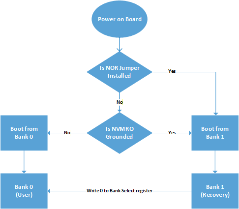
The T2080 will boot from the first bank (bank 0) if the NOR Flash jumper is not installed, and the external NVMRO signal is left floating. If the NOR Flash jumper is installed, or if NVMRO is grounded then then the T2080 will boot from the second bank (bank 1). After boot, writing a 0 to this register will switch to the first bank (bank 0). You cannot write 1 to this register to return to the second bank (bank 1). Please view the below flowchart for an overview of the motherboard boot operation. |
D15 |
D14 |
D13 |
D12 |
D11 |
D10 |
D9 |
D8 |
D7 |
D6 |
D5 |
D4 |
D3 |
D2 |
D1 |
D0 |
0 |
0 |
0 |
0 |
0 |
0 |
0 |
0 |
0 |
0 |
0 |
0 |
0 |
0 |
0 |
D |
Tamper Detect Interface and Action Circuit
NAI is developing an optional Tamper Detect Interface and Action Circuit for improved Security/Cybersecurity requirements. This circuit will offer FIPS 140-3 Level 3 Design Support, Crypto-Key Storage, Secure Boot and Anti-Tamper/Tamper Detect & Sanitize functions. For further information, please contact NAI.
68PPC3A CONNECTOR/PIN-OUT INFORMATION
Rear Panel Connectors
The 68PPC3A SOSA™-aligned 3U OpenVPX SBC is available in two configurations: air-cooled and conduction-cooled. The 68PPC3A follows the OpenVPX “Payload Slot Profile” configured as:
Slot profile: |
SLT3-PAY-1F1F2U1TU1T1U1T-14.2.16 |
Notes
Rear I/O VPX Connectors P0-P2 (Conduction-Cooled)
The 68PPC3A SOSA™-aligned 3U OpenVPX SBC provides interface via the rear VPX connectors.
Rear I/O Summary
P0 - Utility plane. Contains the following signal definitions:
Power: |
Primary +12V, +3.3V_AUX, and System GND |
Geographical Address Pins: |
GA0# - GA4#, GAP# |
Card reset: |
SYSRST# signal |
Non-Volatile Memory Read Only |
NVMRO |
IPMC |
IMPB-SDA-A, IMPB-SDA-B, IMPB-SCL-A, IMPB-SCL-B |
VPX AUX/REF CLK |
(Not used) |
P1 - Defined as Data/Expansion/Control Planes (XMC defined I/O secondary)
High Speed Switched Fabric Interface: |
One fat pipe option (PCIe ver. 2.0 (x1)). |
Ethernet: |
Gig-E port option is available and defined |
P2 - XMC/Built-In I/O (primary)
Rear I/O Utility Plane (P0)
The P0 (Utility) Plane contains the primary power, bus and utility signals for the OpenVPX board. Additionally, several of the user defined pins can be utilized for Geographical Addressing and a parallel SYSRST# signal. Signals defined as N/C currently have no functionality associated and is not required for general operation
UTILITY |
Row |
Row |
Row |
Row |
Row |
Row |
Row |
P0 |
G |
F |
E |
D |
C |
B |
A |
1 |
(+)12V (VS1) |
(+)12V (VS1) |
(+)12V (VS1) |
N/C (NCD1) |
N/C (VS2) |
N/C (VS2) |
N/C (VS2) |
2 |
(+)12V (VS1) |
(+)12V (VS1) |
(+)12V (VS1) |
N/C (NCD2) |
N/C (VS2) |
N/C (VS2) |
N/C (VS2) |
3 |
N/C (VS3) |
N/C (VS3) |
N/C (VS3) |
N/C (NCD3) |
N/C (VS3) |
N/C (VS3) |
N/C (VS3) |
4 |
(IMPB-SCL-B) |
(IMPB-SDA-B) |
GND |
N/C (-12V-AUX) |
GND |
P0-SYSRST# |
NVMRO |
5 |
GAP# |
GA4# |
GND |
(+)3.3V-AUX |
GND |
(IMPB-SCL-A) |
(IMPB-SDA-A) |
6 |
GA3# |
GA2# |
GND |
N/C (+12V-AUX) |
GND |
GA1# |
GA0# |
7 |
N/C (TCK) |
GND |
N/C (TDO) |
N/C (TDI) |
GND |
N/C (TMS) |
N/C (TRST) |
8 |
GND |
(REFCLK-25MHz-) |
(REFCLK-25MHz+) |
GND |
(AUX-CLK-) |
(AUX-CLK+) |
GND |
= Motherboard reserved |
|
= Maintenance reserved |
Rear I/O Data/Expansion/Control Planes (P1)
The 68PPC3A contains one Fat Pipe (data plane), and one Ultra-Thin Pipe (control plane). The data plane specify a high-speed serial interface fabric bus connection - PCIe ver.2.0 (x1). The control plane commands the 68PPC3A via Gig-E (option for a 1GBase-T (SerDes) Interface). Pin-outs for the RGMII & SGMII Ethernet ports are also defined on the P1 I/O plane. Signals defined as N/C currently have no functionality associated or are considered optional and are not required for general operation.
Data |
Row |
Row |
Row |
Row |
Row |
Row |
Row |
P1 |
G |
F |
E |
D |
C |
B |
A |
1 |
GDiscrete1 |
GND |
VPX-DP0-TXN |
VPX-DP0-TXP |
GND |
VPX-DP0-RXN |
VPX-DP0-RXP |
2 |
GND |
VPX-DP1-TXN |
VPX-DP1-TXP |
GND |
VPX-DP1-RXN |
VPX-DP1-RXP |
GND |
3 |
RTC-STDBY |
GND |
N/C |
N/C |
GND |
N/C |
N/C |
4 |
GND |
N/C |
N/C |
GND |
N/C |
N/C |
GND |
5 |
P1-SYSCONn |
GND |
N/C |
N/C |
GND |
N/C |
N/C |
6 |
GND |
N/C |
N/C |
GND |
N/C |
N/C |
GND |
7 |
N/C |
GND |
N/C |
N/C |
GND |
N/C |
N/C |
8 |
GND |
N/C |
N/C |
GND |
N/C |
N/C |
GND |
9 |
(SER-TXD1) |
GND |
ETHS1-TP0P |
ETHS1-TP0N |
GND |
ETHS1-TP1P |
ETHS1-TP1N |
10 |
GND |
ETHS1-TP2P |
ETHS1-TP2N |
GND |
ETHS1-TP3P |
ETHS1-TP3N |
GND |
11 |
(SER-RXD1) |
GND |
ETHS2-TP0P |
ETHS2-TP0N |
GND |
ETH2-TP1P |
ETHS2-TP1N |
12 |
GND |
ETHS2-TP2P |
ETHS2-TP2N |
GND |
ETHS2-TP3P |
ETHS2-TP3N |
GND |
13 |
GPIO-CH1 |
GND |
ETH2-TP0P |
ETH2-TP0N |
GND |
ETH2-TP1P |
ETH2-TP1P |
14 |
GND |
ETH2-TP2P |
ETH2-TP2N |
GND |
ETH2-TP3P |
ETH2-TP3N |
GND |
15 |
MRSTn |
GND |
N/C |
N/C |
GND |
N/C |
N/C |
16 |
GND |
N/C |
N/C |
GND |
N/C |
N/C |
GND |
= Motherboard reserved |
= GPIO (GPIO default) |
= Port 2 - 10/100/1000Base-T (RGMII) |
|||
= RS-232 Maintenance |
= Port 1 - 10/100/1000Base-T (SGMII) |
||||
= Data Plane: PCIe (Gen 2) |
= Port 2 - 10/100/1000Base-T (SGMII) |
||||
XMC/Built-In I/O - Defined Area (P2)
The 68PPC3A contains no 'user defined' I/O data area pin-outs. Pin-outs for the NAI-XMC w/NE6 module (MOD2-I/O) are defined on the P2 I/O plane. In addition to the XMC, there are pin-outs defined for USB 2.0, one storage Ultra-Thin Pipe (SATA), one control plane Thin Pipe (Ethernet), GPIO, and optional audio codec. Signals defined as N/C currently have no functionality associated or are considered optional and are not required for general operation.
Data |
Row |
Row |
Row |
Row |
Row |
Row |
Row |
P2 |
G |
F |
E |
D |
C |
B |
A |
1 |
SER-TXD4 |
GND |
GND |
N/C |
GND |
GPIO-CH6 |
GPIO-CH5 |
HEADSETR- |
HEADSETR+ |
||||||
2 |
GND |
N/C |
N/C |
GND |
N/C |
N/C |
GND |
MIC-BIAS |
MIC-IN |
HEADSETL- |
HEADSETL+ |
||||
3 |
SER-TXD3 |
GND |
GPIO-CH8 |
GPIO-CH7 |
GND |
I2C-DATA |
I2C-CLOCK |
4 |
GND |
USB-2N |
USB-2P |
GND |
N/C |
N/C |
GND |
5 |
SER-RXD4 |
GND |
N/C |
N/C |
GND |
N/C |
N/C |
6 |
GND |
BKPLN-SATA-TXN |
BKPLN-SATA-TXP |
GND |
SATA-RXN-BKPLN |
SATA-RXP-BKPLN |
GND |
7 |
SER-RXD3 |
GND |
ETH1-TP1N |
ETH1-TP1P |
GND |
ETH1-TP0N |
ETH1-TP0P |
8 |
GND |
ETH1-TP3N |
ETH1-TP3P |
GND |
ETH1-TP2N |
ETH1-TP2P |
GND |
9 |
+5V0-USB2 |
GND |
MOD2-DATIO05 |
MOD2-DATIO06 |
GND |
MOD2-DATIO11 |
MOD2-DATIO12 |
10 |
GND |
MOD2-DATIO17 |
MOD2-DATIO18 |
GND |
MOD2-DATIO29 |
MOD2-DATIO30 |
GND |
11 |
GPIO-CH2 |
GND |
MOD2-DATIO19 |
MOD2-DATIO20 |
GND |
MOD2-DATIO21 |
MOD2-DATIO22 |
TAMPER DETECT |
|||||||
12 |
GND |
MOD2-DATIO23 |
MOD2-DATIO24 |
GND |
MOD2-DATIO31 |
MOD2-DATIO32 |
GND |
13 |
GPIO-CH3 |
GND |
MOD2-DATIO01 |
MOD2-DATIO02 |
GND |
MOD2-DATIO03 |
MOD2-DATIO04 |
14 |
GND |
MOD2-DATIO13 |
MOD2-DATIO14 |
GND |
MOD2-DATIO25 |
MOD2-DATIO26 |
GND |
15 |
GPIO-CH4 |
GND |
MOD2-DATIO07 |
MOD2-DATIO08 |
GND |
MOD2-DATIO09 |
MOD2-DATIO10 |
16 |
GND |
MOD2-DATIO15 |
MOD2-DATIO16 |
GND |
MOD2-DATIO27 |
MOD2-DATIO28 |
GND |
= 1x RS-232 or 2x RS422/485 (programmable) |
= GPIO (GPIO default) |
= MOD2 I/O (NAI-XMC Option) |
|||
= USB 2.0 |
= GPIO (Tamper Detect) |
= SATA II |
|||
= I2C support |
= Port 1 - 10/100/1000Base-T (RGMII) |
= Audio Codec (Option) |
|
Note
|
For a more detailed breakdown of the P2 pinouts for the programmable RS232 or RS-422/48 configurations, please refer to the table below: |
Plane/Row |
2x RS-232 ports |
1x RS-422/485 port |
P2-G1 |
SER-TDX4 |
-SER-TDX1 |
P2-G5 |
SER-RDX4 |
-SER-RDX1 |
P2-G3 |
SER-TDX3 |
+SER-TDX1 |
P2-G7 |
SER-RDX3 |
+SER-RDX1 |
Rear User I/O Mapping (NE6 Configuration Only)
Pin-out details (for reference) are shown below, with respect to DATAIO. Additional information on pin-outs can be found in the Module Operational Manuals
|
Slot 2 |
|
Module Signal |
Rear I/O P2 |
Global (MB) |
DATIO1 |
E13 |
|
DATIO2 |
D13 |
|
DATIO3 |
B13 |
|
DATIO4 |
A13 |
|
DATIO5 |
E09 |
|
DATIO6 |
D09 |
|
DATIO7 |
E15 |
|
DATIO8 |
D15 |
|
DATIO9 |
B15 |
|
DATIO10 |
A15 |
|
DATIO11 |
B09 |
|
DATIO12 |
A09 |
|
DATIO13 |
F14 |
|
DATIO14 |
E14 |
|
DATIO15 |
F16 |
|
DATIO16 |
E16 |
|
DATIO17 |
F10 |
|
DATIO18 |
E10 |
|
DATIO19 |
E11 |
|
DATIO20 |
D11 |
|
DATIO21 |
B11 |
|
DATIO22 |
A11 |
|
DATIO23 |
F12 |
|
DATIO24 |
E12 |
|
DATIO25 |
C14 |
|
DATIO26 |
B14 |
|
DATIO27 |
C16 |
|
DATIO28 |
B16 |
|
DATIO29 |
C10 |
|
DATIO30 |
B10 |
|
DATIO31 |
C12 |
|
DATIO32 |
B12 |
|
DATIO33 |
||
DATIO34 |
||
DATIO35 |
||
DATIO36 |
||
DATIO37 |
||
DATIO38 |
||
DATIO39 |
||
DATIO40 |
||
N/A |
SYS GND |
|
CHASSIS |
||
N/C |
||
ETHERNET
The Ethernet Interface Option allows communications and control access to all function modules either via the system BUS or Ethernet ports 1, 2, 3, or 4.
Ethernet 1 |
Ethernet 2 |
Ethernet 3* |
Ethernet 4* |
|
(REF PORT A) |
(REF PORT B) |
(REF PORT C) |
(REF PORT D) |
|
The default IP address: |
192.168.1.16 |
192.168.2.16 |
192.168.3.16 |
192.168.4.16 |
The default subnet: |
255.255.255.0 |
255.255.255.0 |
255.255.255.0 |
255.255.255.0 |
The default gateway: |
192.168.1.1 |
192.168.2.1 |
192.168.3.1 |
192.168.4.1 |
*see Part Number Designation for applicability.
|
Note
|
Actual "as shipped" card Ethernet default IP addresses may vary based upon final ATP configuration(s).) |
Board Addressing
The interface provides two main addressing areas: Onboard and Off-board.
Onboard addressing refers to accessing resources located on the board that is implementing the operation interface (including its modules).
Off-board addressing refers to accessing resources located on another board reachable via VME, PCI, or other bus. Off-board addressing requires a Master/Slave configuration.
The user must always specify if a particular address is Onboard or Off-board. See the command descriptions for the onboard and off-board flags.
Within a particular board (Onboard or Off-board), the address space is broken up into two areas: Motherboard Common Address Space and Module Address Space. All addresses are 32-bit.
Motherboard Common Address Space starts at 0x00000000 and ends at 0x00004000. This is a 4Kx32-bit address space (16 kbytes).
Module Address Space starts at 0x00004000. Module addressing is dynamically configured at startup. NAI boards support between 1 and 6 modules. The minimum module address space size is 4Kx32 (16 kbytes) and module sizes are always a multiple of 4Kx32.
Module addressing is dynamic and cumulative. The first detected module (starting with Slot 1) is given an address of 0x00004000. The 2nd detected Module is given an address of:
First_Detected_Module_Address + First_Detected_Module_Size
|
Note
|
Slots do not define addresses. |
If no module is detected in a module slot, that slot is not given an address. Therefore, if the first detected Module is in Slot 2, then that module address will be 0x00004000. If the next detected module is in Slot 4, then the address of that Module will be:
Second_Detected_Module_Address = First_Detected_Module_Address + First_Detected_Module_Size
If a 3rd Module is detected in Slot 6, then the address of that Module will be:
Third_Detected_Module_Address = Second_Detected_Module_Address + Second_Detected_Module_Size
|
Note
|
Module addresses are calculated at each board startup when the modules are detected. Therefore, if a module should fail to be detected due to malfunction or because it was removed from the motherboard, the addresses of the modules that follow it in the slot sequence will be altered. This is important to note when programming to this interface. |
Users can always retrieve the Module Addresses, Module Sizes and Module IDs from the fixed Motherboard Common address area. This data is set upon each board startup. While the Module Addressing is dynamic, the address where these addresses are stored is fixed. For example, to find the startup address of the module location in Slot 3, refer to the MB Common Address 0x00000408 from the Motherboard Common Addresses table that follows.
Ethernet Wiring Convention
RJ-45 |
T568A Color |
T568B Color |
10/100Base-T |
1000BASE-T |
NAI wiring convention |
1 |
white/green stripe |
white/orange stripe |
TX+ |
DA+ |
ETH-TP0+ |
2 |
green |
orange |
TX- |
DA- |
ETH-TP0- |
3 |
white/orange stripe |
white/green stripe |
RX+ |
DB+ |
ETH-TP1+ |
4 |
blue |
blue |
DC+ |
ETH-TP2+ |
|
5 |
white/blue stripe |
white/blue stripe |
DC- |
ETH-TP2- |
|
6 |
orange |
green |
RX- |
DB- |
ETH-TP1- |
7 |
white/brown stripe |
white/brown stripe |
DD+ |
ETH-TP3+ |
|
8 |
brown |
brown |
DD- |
ETH-TP3- |
68PPC3A PART NUMBER DESIGNATION
Product w/NAI XMC: 68PPC3A-N-AAAPRFIMT0SCZ-XX |
| PROD ID |
XMC | M1 | PROC | SDRAM | IPMC | MECH | ENV | RES | SW | SEC | OPT | SPEC OPT |
-XX | Configuration and Option Descriptions |
|---|---|---|---|---|---|---|---|---|---|---|---|---|---|---|
68PPC3A- |
3U OpeVPX, SBC & Expansion IO |
|||||||||||||
X |
XMC Type (see Note 1) |
|||||||||||||
AAA |
Module Slot 1 (See Available Function Modules) (See Note 2) |
|||||||||||||
P |
Processor Options |
|||||||||||||
R |
DDR3L SDRAM (Size) |
|||||||||||||
F |
SATA SSD Flash |
|||||||||||||
I |
IPMC Option (See Note 3) |
|||||||||||||
M |
Mechanical Options |
|||||||||||||
T |
Temperature/Environmental Options (All boards are Conformal Coated) |
|||||||||||||
0 |
Reserved |
|||||||||||||
S |
Software |
|||||||||||||
C |
Enhanced Security (See Note 4) |
|||||||||||||
Z |
Special Options (See Note 5) |
|||||||||||||
XX |
Special Requirements Dash Code |
Specifications are subject to change without notice.
NOTES
1. |
Module Slot 1 (AAA) Only Serdes/PCIe module only P2 IO 1-32. |
2. |
Module Slot 1 (AAA) Currently optimized for NE6 function module only; all other function module availability pending. |
3. |
IPMC Definition |
4. |
Enhanced Security - Notes |
5. |
Special Options Notes |
NAI Cares
Edit this on GitLab
North Atlantic Industries (NAI) is a leading independent supplier of Embedded I/O Boards, Single Board Computers, Rugged Power Supplies, Embedded Systems and Motion Simulation and Measurement Instruments for the Military, Aerospace and Industrial Industries. We accelerate our clients’ time-to-mission with a unique approach based on a Configurable Open Systems Architecture™ (COSA®) that delivers the best of both worlds: custom solutions from standard COTS components.
We have built a reputation by listening to our customers, understanding their needs, and designing, testing and delivering board and system-level products for their most demanding air, land and sea requirements. If you have any applications or questions regarding the use of our products, please contact us for an expedient solution.
Please visit us at: www.naii.com or select one of the following for immediate assistance: