USER WATCHDOG TIMER MODULE MANUAL
User Watchdog Timer Capability
The User Watchdog Timer (UWDT) Capability is available on the following modules:
-
AC Reference Source Modules
- AC1 - 1 Channel, 2-115 Vrms, 47 Hz - 20kHz
- AC2 - 2 Channels, 2-28 Vrms, 47 Hz - 20kHz
- AC3 - 1 Channel, 28-115 Vrms, 47 Hz - 2.5 kHz
-
Differential Transceiver Modules
- DF1/DF2 - 16 Channels Differential I/O
-
Digital-to-Analog (D/A) Modules
- DA1 - 12 Channels, ±10 VDC @ 25 mA, Voltage or Current Control Modes
- DA2 - 16 Channels, ±10 VDC @ 10 mA
- DA3 - 4 Channels, ±40 VDC @ ±100 mA, Voltage or Current Control Modes
- DA4 - 4 Channels, ±80 VDC @ 10 mA
- DA5 - 4 Channels, ±65 VDC or ±2 A, Voltage or Current Control Modes
-
Digital-to-Synchro/Resolver (D/S) or Digital-to-L( R )VDT (D/LV) Modules
- (Not supported)
-
Discrete I/O Modules
-
DT1/DT4 - 24 Channels, Programmable for either input or output, output up to 500 mA per channel from an applied external 3 - 60 VCC source.
-
DT2/DT5 - 16 Channels, Programmable for either input voltage measurements (±80 V) or as a bi-directional current switch (up to 500 mA per channel).
-
DT3/DT6 - 4 Channels, Programmable for either input voltage measurements (±100 V) or as a bi-directional current switch (up to 3 A per channel).
-
-
TTL/CMOS Modules
- TL1-TL8 - 24 Channels, Programmable for either input or output.
Principle of Operation
The User Watchdog Timer is optionally activated by the applications that require the module’s outputs to be disabled as a failsafe in the event of an application failure or crash. The circuit is designed such that a specific periodic write strobe pattern must be executed by the software to maintain operation and prevent the disablement from taking place.
The User Watchdog Timer is inactive until the application sends an initial strobe by writing the value 0x55AA to the UWDT Strobe register. After activating the User Watchdog Timer, the application must continually strobe the timer within the intervals specified with the configurable UWDT Quiet Time and UWDT Window registers. The timing of the strobes must be consistent with the following rules:
- The application must not strobe during the Quiet time.
- The application must strobe within the Window time.
- The application must not strobe more than once in a single window time.
A violation of any of these rules will trigger a User Watchdog Timer fault and result in shutting down any isolated power supplies and/or disabling any active drive outputs, as applicable for the specific module. Upon a User Watchdog Timer event, recovery to the module shutting down will require the module to be reset.
The Figure 1 and Figure 2 provides an overview and an example with actual values for the User Watchdog Timer Strobes, Quiet Time and Window. As depicted in the diagrams, there are two processes that run in parallel. The Strobe event starts the timer for the beginning of the “Quiet Time”. The timer for the Previous Strobe event continues to run to ensure that no additional Strobes are received within the “Window” associated with the Previous Strobe.
The optimal target for the user watchdog strobes should be at the interval of [Quiet time + ½ Window time] after the previous strobe, which will place the strobe in the center of the window. This affords the greatest margin of safety against unintended disablement in critical operations.
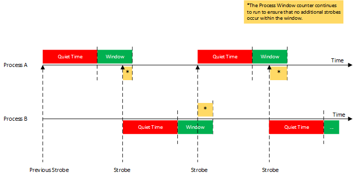 Figure 1. User Watchdog Timer Overview
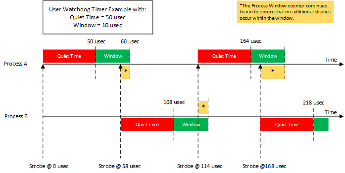 Figure 2. User Watchdog Timer Example
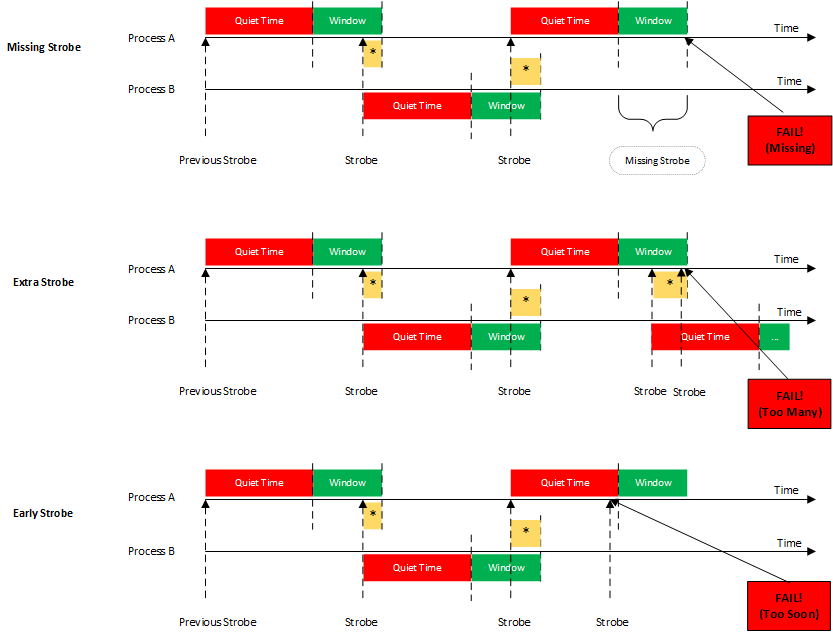 Figure 3. User Watchdog Timer Failures
Register Descriptions
The register descriptions provide the register name, Type, Data Range, Read or Write information, Initialized Value, and a description of the function.
User Watchdog Timer Registers
The registers associated with the User Watchdog Timer provide the ability to specify the UWDT Quiet Time and the UWDT Window that will be monitored to ensure that EXACTLY ONE User Watchdog Timer (UWDT) Strobe is written within the window.
| UWDT Quiet Time | |
| Function: | Sets Quiet Time value (in microseconds) to use for the User Watchdog Timer Frame. |
| Type: | unsigned binary word (32-bit) |
| Data Range: | 0 µsec to 2^32 µsec (0x0 to 0xFFFFFFFF) |
| Read/Write: | R/W |
| Initialized Value: | 0x0 |
| Operational Settings: | LSB = 1 µsec. The application must NOT write a strobe in the time between the previous strobe and the end of the Quiet time interval. In addition, the application must write in the UWDT Window EXACTLY ONCE. |
| UWDT Window | |
| Function: | Writes the window value (in microseconds) to be used for the User Watchdog Timer Frame. |
| Type: | unsigned binary word (32-bit) |
| Data Range: | 0 µsec to 2^32 µsec (0x0 to 0xFFFFFFFF) |
| Read/Write: | R/W |
| Initialized Value: | 0x0 |
| Operational Settings: | LSB = 1 µsec. The application must write the strobe once within the Window time after the end of the Quiet time interval. The application must write in the UWDT Window EXACTLY ONCE. This setting must be initialized to a non-zero value for operation and should allow sufficient tolerance for strobe timing by the application. |
| UWDT Strobe | |
| Function: | Writes the strobe value to be use for the User Watchdog Timer Frame. |
| Type: | unsigned binary word (32-bit) |
| Data Range: | 0x55AA |
| Read/Write: | W |
| Initialized Value: | 0x0 |
| Operational Settings: | At startup, the user watchdog is disabled. Write the value of 0x55AA to this register to start the user watchdog timer monitoring after initial power on or a reset. To prevent a disablement, the application must periodically write the strobe based on the user watchdog timer rules. |
Status and Interrupt
The modules that are capable of User Watchdog Timer support provide status registers for the User Watchdog Timer.
User Watchdog Timer Status
The status register that contains the User Watchdog Timer Fault information is also used to indicate channel Inter-FPGA failures on modules that have communication between FPGA components. There are four registers associated with the User Watchdog Timer Fault/Inter-FPGA Failure Status: Dynamic, Latched, Interrupt Enable, and Set Edge/Level Interrupt.
| Function: | Sets the corresponding bit (D31) associated with the channel’s User Watchdog Timer Fault error. |
|---|---|
| Type: | unsigned binary word (32-bit) |
| Data Range: | 0x0000 0000 to 0xFFFF FFFF |
| Read/Write: | R (Dynamic), R/W (Latched, Interrupt Enable, Set Edge/Level Interrupt) |
| Initialized Value: | 0 |
| User Watchdog Timer Fault/Inter-FPGA Failure Dynamic Status | ||
| User Watchdog Timer Fault/Inter-FPGA Failure Latched Status | ||
| User Watchdog Timer Fault/Inter-FPGA Failure Interrupt Enable | ||
| User Watchdog Timer Fault/Inter-FPGA Failure Set Edge/Level Interrupt | ||
| Bit(s) | Status | Description |
| D31 | User Watchdog Timer Fault Status | 0 = No Fault + 1 = User Watchdog Timer Fault |
| D30:D0 | Reserved for Inter-FPGA Failure Status | Channel bit-mapped indicating channel inter FPGA communication failure detection. |
Interrupt Vector and Steering
When interrupts are enabled, the interrupt vector associated with the specific interrupt can be programmed (typically with a unique number/identifier) such that it can be utilized in the Interrupt Service Routine (ISR) to identify the type of interrupt. When an interrupt occurs, the contents of the Interrupt Vector registers is reported as part of the interrupt mechanism.
In addition to specifying the interrupt vector, the interrupt can be directed (“steered”) to the native bus or to the application running on the onboard ARM processor.
Note
the Interrupt Vector and Interrupt Steering registers are mapped to the Motherboard Common Memory and these registers are associated with the Module Slot position (refer to Function Register Map).
| Interrupt Vector | |
| Function: | Set an identifier for the interrupt. |
| Type: | unsigned binary word (32-bit) |
| Data Range: | 0 to 0xFFFF FFFF |
| Read/Write: | R/W |
| Initialized Value: | 0 |
| Operational Settings: | When an interrupt occurs, this value is reported as part of the interrupt mechanism. |
| Interrupt Steering | |
| Function: | Sets where to direct the interrupt. |
| Type: | unsigned binary word (32-bit) |
| Data Range: | See table |
| Read/Write: | R/W |
| Initialized Value: | 0 |
| Operational Settings: | When an interrupt occurs, the interrupt is sent as specified: |
| Direct Interrupt to VME | 1 |
|---|---|
| Direct Interrupt to ARM Processor (via SerDes) (Custom App on ARM or NAI Ethernet Listener App) | 2 |
| Direct Interrupt to PCIe Bus | 5 |
| Direct Interrupt to cPCI Bus | 6 |
Function Register Map
KEY
| Configuration/Control |
| Measurement/Status |
| USER WATCHDOG TIMER REGISTERS | |||||
| OFFSET | REGISTER NAME | ACCESS | OFFSET | REGISTER NAME | ACCESS |
| 0x01C0 | UWDT Quiet Time | R/W | |||
| 0x01C4 | UWDT Window | R/W | |||
| 0x01C8 | UWDT Strobe | R/W | |||
| STATUS REGISTERS | |||||
| *When an event is detected, the bit associated with the event is set in this register and will remain set until the user clears the event bit. Clearing the bit requires writing a 1 back to the specific bit that was set when read (i.e., write-1-to-clear, writing a “1” to a bit set to “1” will set the bit to “0”). | |||||
| OFFSET | REGISTER NAME | ACCESS | OFFSET | REGISTER NAME | ACCESS |
| 0x09B0 | Dynamic Status | R | |||
| 0x09B4 | Latched Status* | R/W | |||
| 0x09B8 | Interrupt Enable | R/W | |||
| 0x09BC | Set Edge/Level Interrupt | R/W | |||
| INTERRUPT REGISTERS | |||||
| The Interrupt Vector and Interrupt Steering registers are mapped to the Motherboard Memory Space and these addresses are absolute based on the module slot position. In other words, do not apply the Module Address offset to these addresses. | |||||
| OFFSET | REGISTER NAME | ACCESS | OFFSET | REGISTER NAME | ACCESS |
| 0x056C | Module 1 Interrupt Vector 28 - User Watchdog Timer Fault/Inter-FPGA Failure | R/W | 0x066C | Module 1 Interrupt Steering 28 - User Watchdog Timer Fault/Inter-FPGA Failure | R/W |
| 0x076C | Module 2 Interrupt Vector 28 - User Watchdog Timer Fault/Inter-FPGA Failure | R/W | 0x086C | Module 2 Interrupt Steering 28 - User Watchdog Timer Fault/Inter-FPGA Failure | R/W |
| 0x096C | Module 3 Interrupt Vector 28 - User Watchdog Timer Fault/Inter-FPGA Failure | R/W | 0x0A6C | Module 3 Interrupt Steering 28 - User Watchdog Timer Fault/Inter-FPGA Failure | R/W |
| 0x0B6C | Module 4 Interrupt Vector 28 - User Watchdog Timer Fault/Inter-FPGA Failure | R/W | 0x0C6C | Module 4 Interrupt Steering 28 - User Watchdog Timer Fault/Inter-FPGA Failure | R/W |
| 0x0D6C | Module 5 Interrupt Vector 28 - User Watchdog Timer Fault/Inter-FPGA Failure | R/W | 0x0E6C | Module 5 Interrupt Steering 28 - User Watchdog Timer Fault/Inter-FPGA Failure | R/W |
| 0x0F6C | Module 6 Interrupt Vector 28 - User Watchdog Timer Fault/Inter-FPGA Failure | R/W | 0x106C | Module 6 Interrupt Steering 28 - User Watchdog Timer Fault/Inter-FPGA Failure | R/W |
REVISION HISTORY
| Motherboard Manual - Status and Interrupts Revision History | ||
| Revision | Revision Date | Description |
| C | 2021-11-30 | C08896; Transition manual to docbuilder format - no technical info change. |
DOCS.NAII REVISIONS
| Revision Date | Description |
|---|---|
| 2026-03-02 | Formatting updates to document; no technical changes. |