INTRODUCTION
As a leading manufacturer of smart function modules, NAI offers over 100 different modules that cover a wide range of I/O, measurement and simulation, communications, Ethernet switch, and SBC functions. Our CM5 combination module offers users the functionality of two COSA® smart function modules in one physical module. Based on NAI’s FTB (MIL-STD-1553B) and DT4 modules, the CM8 provides two MIL-STD- 1553B, Notice 2 compliant interface channels, and twelve channels of discrete I/O that are programmable for either input or output per channel. This user manual is designed to help you get the most out of our CM5 smart function module.
CM5 Overview
NAI’s CM8 module offers a wide range of features designed to suit a variety of system requirements, including:
MIL-STD-1553B (FTB Module-Type) Features
Independent Dual-Redundant Channels: The FTB function provides two dual-redundant MIL-STD-1553B interface channels. Each channel can be configured to act as a Bus Controller (BC), Remote Terminal (RT), Bus Monitor (BM), or RT/BM combined mode. This flexibility allows for versatile operation and redundancy in critical systems.
Assisted Mode (AM): The FTB function utilizes a built-in secondary (ARM) processor dedicated to ‘assisting’ the movement of 1553 messages from the 1553 device to host interface, minimizing host CPU activity (reads & writes to device), reducing application memory required on the host, and improving data transfer time between 1553 device and host interface while also reducing data transfer delays.
Ample On-Board Memory: With a substantial 64K words of on-board memory per channel, this function offers ample storage capacity for data and messages, facilitating efficient data handling and processing.
IP-Core Register Compatibility: Users familiar with the DDC™ family of devices will appreciate that the function’s IP-core registers are compatible with these devices. This compatibility ensures seamless integration into existing systems and reduces the learning curve for engineers already familiar with DDC™ products.
Message Retry Policy: The FTB function provides the ability to configure and set a message retry policy, proving invaluable in ensuring data integrity and system reliability, particularly in environments where communication errors may occur.
Message Scheduling Capability: This feature allows precise timing and coordination of messages, making it ideal for applications that require synchronized data exchange.
Asynchronous Message Capability: The FTB function supports asynchronous messaging, which is crucial for real-time systems where data needs to be transmitted and received without fixed time intervals. This feature ensures efficient communication in dynamic environments.
Message FIFO Capability: The inclusion of a message FIFO (First-In-First-Out) capability enhances data management and flow control. Users can optimize data handling and prioritize messages as needed, contributing to system efficiency.
Discrete I/O (DT4 Module-Type) Features
24 Channels of Programmable Discrete Input/Output: The DT4 module features 12 channels programmable for either discrete input or output that provide the following:
- Input - voltage or contact sensing with programmable, pull-up/pull-down current sources, eliminating the need for external resistors or mechanical jumpers.
- Output - programmable current source (high-side), sink (low-side) or push-pull switching up to 500 mA per channel from an applied 3- 60V external VCC source (or sink to ISO-GND).
Current Sharing: The module enables current sharing* by connecting multiple outputs in parallel, capable of sinking or sourcing up to 2A per bank, enhancing your system’s capacity and reliability.
(*) Current Share: The maximum output load per-channel is ±0.5A. Channels can be connected and operated in parallel to provide > 0.5A to act as a single channel. The load current between paralleled channels cannot be effectively characterized and is not expected to be equal due to factors including:
Channel/bank position, module position, motherboard/system platform configuration, operating temperature range including external application/configuration influences (e.g., external cabling).
Therefore, when operating in shared current (parallel channel) configuration, it is recommended to de-rate the per-channel maximum current output to at least 66% (or 333 mA/channel) to ensure that no single channel is overburdened by handling most of the load current.
For example: If the maximum continuous load current is expected to be 1A: 1/0.33 ≅ 3 channels (minimum).
Inrush Current Handling: The DT4 module can efficiently handle high inrush current loads, such as connecting two #327 incandescent lamps in parallel, without compromising performance.
Dual Turn-On Application Support: The module supports ‘dual turn-on’ applications, such as dual series ‘key’ missile launch control, providing seamless control in critical operations.
Debounce Circuitry: Programmable debounce circuitry with selectable time delay eliminates false signals caused by relay contact bounce, ensuring accurate data acquisition.
Background Built-In-Test (BIT): All channels have continuous background Built-In-Test (BIT), which provides real-time channel health to ensure reliable operation in mission-critical systems. This feature runs in the background and is transparent in normal operations.
Input Diagnostics: The DT4 module can sense broken input connections and detect if inputs are shorted to +V or ground, allowing for early detection and troubleshooting.
Voltage and Current Readings: The module offers the ability to read I/O voltage and output current, facilitating improved diagnostics and load status identification (indicates if load is connected).
Enhanced Functionality Features: In addition to offering the same functionality as the DT1 standard function (SF) module, the DT4 includes the following enhanced features:
- Enhanced Input Mode - Pulse Measurements, Transition Timestamps, Transition Counters, Period Measurement, and Frequency Measurement.
- Enhanced Output Mode - PWM Output and Pattern Generator Output.
MIL-STD-1553B
The MIL-STD-1553B communications function is like the standard FTB communications function module (FTB may be used as a reference/guide within the context of this document).
Principle of Operation
The CM8 provides (2) channels of dual-redundant MIL-STD-1553B communication buses (FTB module-type).MIL-STD-1553 is a military standard that defines the characteristic for a Digital Time Division Command/Response Multiplexed Data Bus. The 1553 data bus is a dual-redundant, bi-directional, Manchester II encoded data bus with a high bit error reliability. It is used commonly for both military and civilian applications in avionics, aircraft and spacecraft data handling.
Table 1 provides a summary of the MIL-STD-1553 characteristics.
Summary of MIL-STD-1553 Characteristics
| Terminal Types | Bus Controller Remote Terminal Bus Monitor |
|---|---|
| Number of Remote Terminals | Maximum of 31 |
| Transmission Technique | Half-duplex |
| Operation | Asynchronous |
| Encoding | Manchester II bi-phase level |
| Fault Tolerance | Typically, Dual Redundant Bus, which means there are two independent bus networks (one bus is called the Primary or “A” bus and the other is the Secondary or “B” bus. 1553 messages are usually only transmitted on either the A or B bus network at a time, but it does not usually matter which bus is used for the message transfer - devices on the 1553 network are supposed to handle messages on either the A or B bus with equal priority. |
| Coupling | Transformer or direct |
| Data Rate | 1 MHz |
| Word Length | 20 bits |
| Data Bits/Word | 16 bits |
| Message Length | Maximum of 32 Data Words |
| Protocol | Command/response |
| Message Formats | Bus Controller to Remote Terminal (BC-RT message) Remote Terminal to Bus Controller (RT-BC message) Remote Terminal to Remote Terminal (RT-RT message) Broadcast System control (Tx and Rx Mode codes) |
The MIL-STD-1553 Data Bus is defined as a twisted shielded pair transmission line consisting of the main bus and a number of stubs. There is one stub for each remote terminal connected to the bus. The main bus is terminated at each end with a resistance equal to the cable’s characteristic impedance (± 2%). This termination makes the data bus behave electrically like an infinite transmission line. Stubs, which are added to the main bus to connect the terminals, provide “local” loads, and produce impedance mismatch where added. This mismatch, if not properly controlled, produces electrical reflections and degrades the performance of the main bus. Table 2 provides a summary of the MIL-STD-1553 Transmission Media characteristics.
Summary of MIL-STD-1553 Transmission Media Characteristics
| Cable Type | Twisted Shielded Pair |
|---|---|
| Capacitance | 30.0 pF/ft max, wire to wire |
| Characteristic Impedance | 70.0 to 85.0 ohms at 1 MHz |
| Cable Attenuation | 1.5 dB/100 ft. max, at 1 MHz |
| Cable Twists | 4 Twists per ft., minimum |
| Shield Coverage | 90% minimum |
| Cable Termination | Cable impedance (± 2%) |
| Direct Coupled Stub Length | Maximum of 1 foot |
| XFMR Coupled Stub Length | Maximum of 20 feet |
Each 1553 channel on the FTA-FTF module employs a Sital Technology BRM1553D core, which is based on Sital’s proven 1553 IP cores, with DDC® Enhanced Mini-Ace® compatible interface. The core may operate in Bus Controller (BC), Remote Terminal (RT), Bus Monitor (BM) or RT/BM combined mode.
Bus Controller
The Bus Controller (BC) provides data flow control for all transmissions on the bus. In addition to initiating all data transfers, the BC must transmit, receive, and coordinate the transfer of information on the data bus. All information is communicated in command/response mode – the BC sends a command to the RTs, which reply with a response, unless the message is BC→broadcast receive message, in which case, there will be no RT response.
Remote Terminal
The Remote Terminal (RT) is a device designed to interface various subsystems with the 1553 data bus. The RT receives and decodes commands from the BC, detects any errors and reacts to those errors. The RT must be able to properly handle both protocol errors (missing data, extra words, etc.) and electrical errors (waveform distortion, rise time violations, etc.). RT characteristics include:
- Up to 31 Remote Terminals can be connected to the data bus
- Each Remote Terminal can have 31 Sub addresses, where SA 0 and SA 31 signify a Mode code message. In which case the data word count would be the Mode Code number.
- No Remote Terminal shall speak unless spoken to first by the Bus Controller and specifically commanded to transmit.
Bus Monitor
The Bus Monitor (BM) listens to all messages on the data bus and records selected activities. The BM is a passive device that collects data for real-time or post capture analysis. The BM can store all or portions of traffic on the bus, including electrical and protocol errors. BMs are primarily used for instrumentation and data bus testing.
MIL-STD-1553 Protocol
MIL-STD-1553 data bus system consists of a Bus Controller (BC) controlling multiple Remote Terminals (RT) all connected by a data bus providing a single data path between the Bus Controller and all the associated Remote Terminals. There may also be one or more Bus Monitors (BM); however, Bus Monitors are specifically not allowed to take part in data transfers and are only used to capture or record data for analysis.
Message Formats
The following transactions are allowed between the BC and a specific RT:
- BC to RT Transfer - The Bus Controller sends one 16-bit receive command word, immediately followed by 1 to 32 16-bit data words. The selected Remote Terminal then sends a single 16-bit Status word
- RT to BC Transfer - The Bus Controller sends one transmit command word to a Remote Terminal. The Remote Terminal then sends a single Status word, immediately followed by 1 to 32 data words.
- Mode Command Without Data Word (Transmit) - The Bus Controller sends one command word with a Sub-address of 0 or 31 signifying a Mode Code type command. The Remote Terminal responds with a Status word
- Mode Command with Data Word (Transmit) - The Bus Controller sends one command word with a Sub-address of 0 or 31 signifying a Mode Code type command. The Remote Terminal responds with a Status word immediately followed by a single Data word
- Mode Command with Data Word (Receive) - The Bus Controller sends one command word with a Sub-address of 0 or 31 signifying a Mode Code type command immediately followed by a single data word. The Remote Terminal responds with a Status word
The following transaction is allowed between the BC and a pair of RTs:
- RT to RT Transfers - The Bus Controller sends out one receive command word immediately followed by one transmit command word. The transmitting Remote Terminal sends a Status word to the BC, immediately followed by 1 to 32 data words to the receiving RT. The receiving Terminal then sends its Status word to the BC.
The following are broadcast transactions that are allowed between the BC and all capable RTs:
- BC to RT(s) Transfers - The Bus Controller sends one receive command word with a Terminal address of 31 signifying a broadcast type command, immediately followed by 0 to 32 data words. All Remote Terminals will accept the data but will not respond back to the BC.
- RT to RT(s) Transfers - The Bus Controller sends out one receive command word with a Terminal address of 31 signifying a broadcast type command, immediately followed by one transmit command. The transmitting Remote Terminal sends a Status word immediately followed by 1 to 32 data words to all other RT(s). All Remote Terminals will accept the data but will not respond back to the BC.
- Mode Code without Data Word (Broadcast) - The Bus Controller sends one command word with a Terminal address of 31 signifying a broadcast type command and a sub-address of 0 or 31 signifying a Mode Code type command. No Remote Terminals will respond back to the BC.
- Mode Code with Data Word (Broadcast) - The Bus Controller sends one command word with a Terminal address of 31 signifying a broadcast type command and a sub-address of 0 or 31 signifying a Mode Code type command, immediately followed by one Data word, if it is an Rx Mode code. No Remote Terminals will respond.
Message Components
The following are three components that make up the 1553 messages:
- Command Word
- Data Word
- Status Word
Each word type is 20 bits in length. The first 3 bits are used as a synchronization field, thereby allowing the decode clock to re-sync at the beginning of each new word. The next 16 bits are the information field. The last bit is the parity bit. Parity is based on odd parity for the single word.
Command Word
The Command Word specifies the function that the Remote Terminal is to perform.
The RT Address field states which unique remote terminal the command is intended for (no two terminals may have the same address). Note the address of 0x00 (00000b) is a valid address, and the address 0x1F (11111b) is always reserved as a broadcast address. The maximum number of terminals the data bus can support is 31.
The Transmit/Receive bit defines the direction of information flow and is always from the point of view of the Remote Terminal. A transmit command (logic 1) indicates that the Remote Terminal is to transmit data, while a receive command (logic 0) indicates that the Remote Terminal is going to receive data
The Sub-Address/Mode Code and Word Count/Mode Code fields are defined as follows:
| Sub-Address/Mode Command Field | Word Count/Mode Code Field |
|---|---|
| 0x00 (00000b) or 0x1F (11111b) indicates Mode Code Command | Mode Code number to be performed |
| 0x01 (00001b) to 0x1E (11110b) indicates the Sub-Address 1 to Sub-Address 30 | Word Count - note 0x00 (00000b) is decoded as 32 data words |
Data Word
The Data Word contains the actual information that is being transferred within a message. Data Words can be transmitted by either a Remote Terminal (Transmit command) or a Bus Controller (Receive command).
Status Word
When the Remote Terminal receives a message, it will respond with a Status Word. The Status Word is used to convey to the Bus Controller whether a message was properly received or to convey the state of the Remote Terminal (i.e., service request, busy, etc.).
The RT Address in the Status Word should match the RT Address within the Command Word that the Remote Terminal received. With a RT-RT Transfer message, the RT address within either Status Word received (Rx or Tx), should match the RT address within the corresponding Command word sent (Rx or Tx)
| Status Bit | Description |
|---|---|
| Message Error (Bit 9) | This bit is set by the Remote Terminal upon detection of an error in the message or upon detection of an invalid message (i.e. Illegal Command). The error may occur in any of the Data Words within the message. When the terminal detects an error and sets this bit, none of the data received within the message is used. |
| Instrumentation (Bit 10) | This bit is always set to logic 0. |
| Service Request (Bit 11) | This bit is set to a logic 1 by the subsystem if servicing is needed. This bit is typically used when the Bus Controller is “polling” terminals to determine if they require processing. |
| Broadcast Command Received (Bit 15) | This bit indicates that the Remote Terminal received a valid broadcast command. On receiving a valid broadcast command, the Remote Terminal sets this bit to logic 1 and suppresses the transmission of its Status Word. The Bus Controller may issue a Transmit Status Word or Transmit Last Command Word Mode Code to determine if the Remote Terminal received the message properly. |
| Busy (Bit 16) | This bit indicates to the Bus Controller that the Remote Terminal is unable to move data between the Remote Terminal and the Sub-system in compliance to a command from the Bus Controller. In the earlier days of 1553, the Busy bit was required because many subsystem interfaces (analog, synchros, etc.) were much slower compared to the speed of the multiplex data bus. So instead of losing data, a terminal was able to set the Busy bit indicating to the Bus Controller to try again later. As new systems have been developed, the need for the busy bit has been reduced. |
| Subsystem Flag (Bit 17) | This bit provides “health” data regarding the subsystems to which the Remote Terminal is connected. Multiple subsystems may logically “OR” their bits together to form a composite health indicator. |
| Dynamic Bus Control Acceptance Bit (Bit 19) | This bit informs the Bus Controller that the Remote Terminal has received the Dynamic Bus Control Mode Code and has accepted control of the bus. The Remote Terminal, on transmitting its status word, becomes the Bus Controller. The Bus Controller, on receiving the status word from the Remote Terminal with this bit set, ceases to function as the Bus Controller and may become a Remote Terminal or Bus Monitor. |
| Terminal Flag (Bit 20) | This bit informs the Bus Controller of a fault or failure within the Remote Terminal. A logic 1 indicates a fault condition. |
External RT Address and Auto Start-up Modes
External discrete signals are available to support “hardwired” RT Address and configuration as well as start-up modes for MIL-STD-1760A.
External RT Address
The 1553 modules are completely software RT Address programmable and configurable. Notice 2 of the MIL-STD-1553 standard requires that the Remote Terminal address be wire-programmable from an external I/O connector, and the Remote Terminal perform an odd parity test upon on the wired terminal address. An open circuit on an address line is detected as a logic “1” and connecting the address line to ground is detected as a logic “0”. The 1553 modules provided the ability to externally set the RT Address and Parity via discrete signals (CHx-RT-ADDR (0-4) and CHx- PARITY). These discrete signals are considered additional and optional based on specific application requirements. The discrete signals are single-ended and System-GND referenced. Because of the platform (module-thru-board) available physical pin limitations, only one set of discrete signals are provided for a channel (CH) pair (channel pair 1 = CH1, CH2 and channel pair 2 = CH3, CH4). The discrete pins re provided for the odd-numbered channel, which will use these signals directly. The even channel of the channel pair will use these same pins, but the RT addressing for the even channel will be set as a “hard +1” offset from the odd-channel discrete pattern.
For example:
If the CH1 external pins are either grounded or left open to yield:
CH1-RT-ADDR0-4 pins Parity pin = <sub>(MSB)</sub> 01101 <sub>(LSB)</sub> 0 (defined as Odd Parity) =0xD (13d)
and the hard offset for CH2 is “1” (0x1)
then, the CH1 RT address is 0xD (13d) (wired) and the CH2 RT address will be 0xE (14d) (wired plus the hard offset).
| DISCRETE SIGNAL PIN | DESCRIPTION (Grounding a pin = “0”, leaving a pin open = “1”. Unit signal pins are defaulted “open = 1”) |
|---|---|
| CHx-RT-ADDR0 thru CHx-RT-ADDR4 | Five (5) External RT address signal pins, binary bit-weighted (ADDR0=LSB); for applying a “hardwire” RT address (special applications only). MSB - (…ADDR4, …ADDR3, …ADDR2, …ADDR1, …ADDR0) - LSB |
| CHx-PARITY | Used in conjunction with external RT address signal pins. A single bit that complements the parity of CHx-RT-ADDR wire to odd parity. If the wrong parity is detected by core, only Broadcast commands would be valid for the core. If not masked, an interrupt will be generated in the event of wrong parity. |
Start-up Modes
In addition to supporting external RT Addressing, the 1553 modules provide discrete signals (CHx-STANDARD and CHx-MODE0) to support MIL-STD-1760 auto start-up modes.
| DISCRETE SIGNAL PIN | DESCRIPTION (Grounding a pin = “0”, leaving a pin open = “1”. Unit signal pins are defaulted “open = 1”) |
|---|---|
| CHx-STANDARD | ’1’ - Support for MIL-STD-1760. Will power up as RT with Busy bit set. ‘0’ - Powers up as inactive BC or Idle. |
| CHx-MODE0 | ’1’ - Disables the BC mode even if software enables BC. ‘0’ - BC mode controlled by software. |
Assisted Mode (AM)
The FTA-FTF 1553 modules have been improved to include the “Assisted Mode (AM)” feature.
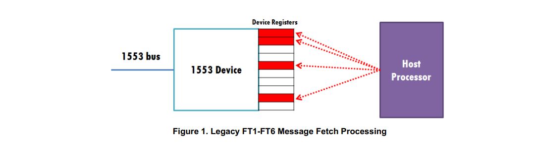
In the legacy FT1-FT6 modules, the 1553 messages are fetched from the 1553 device by accessing device registers directly from the host application as shown in Figure 1. The dotted lines indicate read/write access over the bus interface. The bus interface in some cases may be relatively “slow” (ex. Ethernet interface). In this design, four bus accesses are required from the host to fetch one new 1553 message. The number of accesses increases proportionately with the number of 1553 messages to fetch from the 1553 device.
Figure 1. Legacy FT1-FT6 Message Fetch Processing
The FTA-FTF 1553 modules utilize the secondary (ARM) processor built into the module that is dedicated for the purpose of “assisting” the movement of 1553 messages from the 1553 device to the host interface. This is made possible through a system of FIFOs that carry command and response messages to and from the host CPU to a bare metal application running on the secondary processor (refer to Diagram B in Figure 2). In addition, these modules have the option of funneling all 1553 messages (per channel) to a 4k byte Message FIFO (refer to Diagram A in Figure 2) that is accessible from the host.
Figure 2. AM FIFO and Bus Access
In Figure 2, the dotted lines indicate slower bus read/write accesses (PCI, Ethernet) whereas the solid lines indicate fast bus accesses. When the Message FIFO is utilized (Diagram A), the Message FIFO is filled as new 1553 messages arrive. Moving the 1553 messages from the Message FIFO to the Host Processor requires 2 “slower” bus accesses to fetch all the new 1553 messages that are in the Message FIFO.
If the Message FIFO is not utilized (Diagram B only), for example to fully support DDC API compatibility, 2 writes and at least 2 reads via the “slower” bus is required to fetch one new 1553 message. The write access to the Command FIFO initiates the transfer of 1553 messages from the device to the Response FIFO and when the transfer is complete, the host can read the Response FIFO. In DDC API compatibility mode, the benefits of the “assisted” design provide significantly improved response times compared to the legacy FT module(s), especially with bulk 1553 transfers.
Figure 3 and Table 3 depict the latent time (time required for 1553 message(s) transfer from 1553 device to host memory when initiated by the host CPU) as a function of the number of 1553 messages being transferred. The three candidates for comparison are (1) Assisted Module running in Message FIFO Mode, (2) Assisted Module running in Standard Mode and (3) the Non-Assisted (Legacy) FT Module.
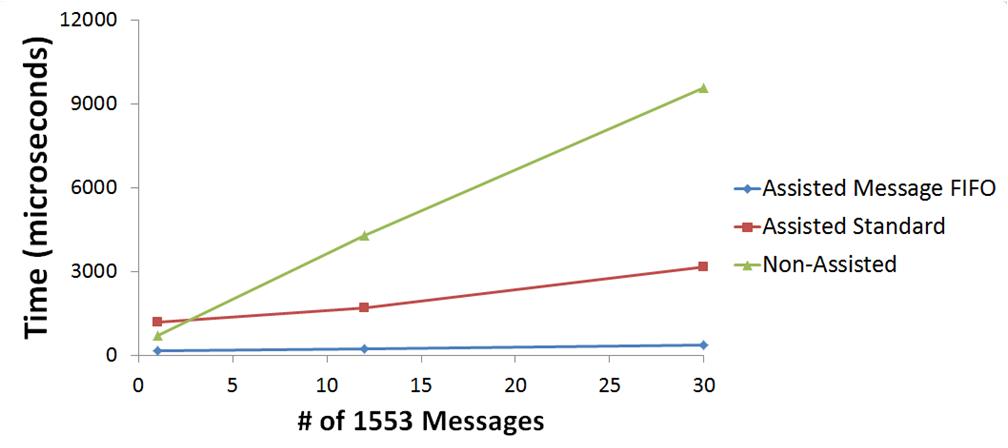
Figure 3. AM Transfer Comparisons
Average and Worst-Case Latent Times in microseconds
| 1553 Msgs | Assisted Message FIFO | Assisted Standard | Non-Assisted | |||
| Average | Worst-Case | Average | Worst-Case | Average | Worst-Case | |
| 1 | 163.630 | 182.445 | 1169.992 | 1193.958 | 695.578 | 705.235 |
| 12 | 239.0805 | 261.298 | 1698.532 | 1735.622 | 4286.303 | 5574.973 |
| 30 | 366.4155 | 399.722 | 3179.139 | 3198.554 | 9566.732 | 9610.468 |
The benefits of this approach include:
- Reduced number of host CPU reads and writes to the device.
- Reduced host memory footprint (less application memory required on the host).
- Lower latency from 1553 bus to host memory.
Status and Interrupts
The FTB function of the combination module provide registers that indicate faults or events. Refer to “Status and Interrupts Module Manual” for the Principle of Operation description.
Module Common Registers
The FTB function of the combination module includes module common registers that provide access to module-level bare metal/FPGA revisions and compile times, unique serial number information, and temperature/voltage/current monitoring. Refer to “Module Common Registers Module Manual” for detailed information.
Register Descriptions
The register descriptions provide the register name, Type, Data Range, Read or Write information, Initialized Value, a description of the function and, in most cases, a data table.
Assisted Mode Registers
The Assisted Mode registers are comprised of registers that support the AM Command and AM 1553 Message FIFOs
AM Commands Registers
The registers associated with the AM Commands are divided into the following:
- Command FIFO Management (FIFO Buffer, FIFO Count, FIFO Update)
- Response FIFO Management (FIFO Buffer, FIFO Count)
The Command FIFO registers are used by the host to send commands to the AM processor to configure and operate the 1553 IP core. For every command sent from the host processor to the AM processor, the AM processor responds with a message that is sent to the host processor via the Response FIFO Buffer. The content of the response message will vary depending on the command and may contain configuration information, status information or 1553 data.
AM Command FIFO Buffer
Function: Used to communicate with the 1553 core via the AM (secondary) processor.
Type: unsigned binary word (32-bit)
Data Range: 0x0000 0000 to 0xFFFF FFFF
Read/Write: W
Initialized Value: 0
Operational Settings: The host writes a command message to the AM Command FIFO Buffer and it is read out by the secondary processor. The secondary processor acts on the 1553 core based on the command that was read out. The AM processor will be unaware any new command messages in the AM Command FIFO Buffer until an update is performed by writing a ‘1’ to the AM Command FIFO Update register.
AM Command FIFO Count
Function: This register contains the value representing the number of 32-bit words that are currently loaded in the AM Command FIFO Buffer.
Type: unsigned binary word (32-bit)
Data Range: 0x0000 0000 to 0xFFFF FFFF
Read/Write: R
Initialized Value: 0
Operational Settings: When the host writes a command message to the AM Command FIFO Buffer, the value of the AM Command FIFO Count represents the number of 32-bit words contained in the command message. Once the message is fully read out by the AM processor, the AM Command FIFO Count goes to zero.
AM Command FIFO Update
Function: This register is used to update the AM Command FIFO count as it is presented to the AM processor. The purpose of this register is to ensure that the AM Command FIFO Buffer does not present incomplete command messages to the AM processor.
Type: unsigned binary word (32-bit)
Data Range: 0x0000 0000 to 0x0000 0001
Read/Write: W
Initialized Value: 0
Operational Settings: The user should write a ‘1’ to this register to update the AM Command FIFO count as it is seen from the AM processor. The proper way to handle sending commands to the AM processor is to write a full command message to the AM Command FIFO Buffer, then update the count by writing a ‘1’ to the AM Command FIFO Update register.
AM Response FIFO Buffer
Function: Used by the AM (secondary) processor to send response messages to the host.
Type: unsigned binary word (32-bit)
Data Range: 0x0000 0000 to 0xFFFF FFFF
Read/Write: R
Initialized Value: 0
Operational Settings: After the host writes a valid command message to the AM Command FIFO Buffer and it is read out by the AM processor, the AM processor acts on the 1553 core based on the command type. Once the action is completed, the AM processor sends a response to the host processor via the AM Response FIFO Buffer.
AM Response FIFO Count
Function: This register contains the value that represents the number of 32-bit words that are present in the AM Response FIFO Buffer.
Type: unsigned binary word (32-bit)
Data Range: 0x0000 0000 to 0xFFFF FFFF
Read/Write: R
Initialized Value: 0
Operational Settings: When a command is sent from the host to the AM processor and it completes the commanded task, it loads the AM Response FIFO with a response message and the AM Response FIFO Count is updated with the number of 32-bit words that are contained in the response message. Once the host reads out the full response message from the AM Response FIFO Buffer, the AM Response FIFO Count will read zero.
AM 1553 Message FIFO Registers
The Message FIFO Management registers consists of the FIFO Buffer, FIFO Count, FIFO Clear command, and the FIFO Threshold which specify threshold associated with for the “1553 Message FIFO Almost Full” status bits in the Channel Status register.
AM 1553 Message FIFO Buffer
Function: When the channel is operating in Message FIFO mode, 1553 messages are stored in the 1553 Message FIFO Buffer.
Type: unsigned binary word (32-bit)
Data Range: 0x0000 0000 to 0xFFFF FFFF
Read/Write: R
Initialized Value: 0
Operational Settings: When the channel is configured for Message FIFO mode, new 1553 messages (comprising 1553 data words, 1553 status words, timestamp and message status information) are stored in the 1553 Message FIFO Buffer and the host can perform a block read on this register to read out a chain of 1553 messages in a single transaction. The number of 32-bit words to read out of the 1553 Message FIFO Buffer is reported in the 1553 Message FIFO Count register. Refer to Appendix A - 1553 Receive Message FIFO to decode the single 1553 message or a chain of 1553 messages read from this buffer.
AM 1553 Message FIFO Count
Function: While the channel is operating in Message FIFO mode, the number of 32-bit words in the 1553 Message FIFO Buffer is reported in this register.
Type: unsigned binary word (32-bit)
Data Range: 0x0000 0000 to 0xFFFF FFFF
Read/Write: R
Initialized Value: 0
Operational Settings: When the channel is configured for Message FIFO mode, new 1553 messages (comprising 1553 data words, 1553 status words, timestamp, and message status information) are stored in the 1553 Message FIFO Buffer. The 32-bit count of a 1553 message can vary depending on the 1553 message type and 1553 data payload size. This register provides the count of 32-bit words that are currently present in the 1553 Message FIFO Buffer instead of providing the count of 1553 messages. When retrieving data from the 1553 Message FIFO Buffer, use the 1553 Message FIFO Count to obtain all 1553 messages and refer to Appendix A - 1553 Receive Message FIFO to decode 1553 messages.
AM 1553 Message FIFO Clear
Function: When the channel is operating in Message FIFO mode, this register is used to clear the 1553 Message FIFO Buffer.
Type: unsigned binary word (32-bit)
Data Range: 0x0000 0000 to 0xFFFF FFFF
Read/Write: W
Initialized Value: 0
Operational Settings: Write a ‘1’ to this register to clear the 1553 Message FIFO Buffer. Once the buffer is cleared, the 1553 Message FIFO Count register should read zero.
AM 1553 Message FIFO Threshold
Function: Set the “1553 Message FIFO Almost Full” status threshold value.
Type: unsigned binary word (32-bit)
Data Range: 1 to 1002
Read/Write: R/W
Initialized Value: 512
Operational Settings: This register sets the “1553 Message FIFO Almost Full” threshold such that when the number of 32-bit words reach or surpass the threshold value, the 1553 Message FIFO Almost Full status bit will report a ‘1’. If interrupts are enabled for this status bit, an interrupt will be generated when the number of 32-bit words reach or surpass the threshold value.
Auxiliary Registers
Reset
Function: A write to this register causes a reset of the channel/core.
Type: unsigned binary word (32-bit)
Data Range: 0x0000 0000 to 0x0000 000F
Read/Write: W (Reset)
Initialized Value: 0
Operational Settings: Reset - Write a 1 to reset the core.
Reset
| D31 | D30 | D29 | D28 | D27 | D26 | D25 | D24 | D23 | D22 | D21 | D20 | D19 | D18 | D17 | D16 |
|---|---|---|---|---|---|---|---|---|---|---|---|---|---|---|---|
| 0 | 0 | 0 | 0 | 0 | 0 | 0 | 0 | 0 | 0 | 0 | 0 | 0 | 0 | 0 | 0 |
| D15 | D14 | D13 | D12 | D11 | D10 | D9 | D8 | D7 | D6 | D5 | D4 | D3 | D2 | D1 | D0 |
| 0 | 0 | 0 | 0 | 0 | 0 | 0 | 0 | 0 | 0 | 0 | 0 | 0 | 0 | 0 | D |
RT Address from Backplane
Function: Provides the Remote Terminal address and the parity.
Type: unsigned binary word (32-bit)
Data Range: See table
Read/Write: R
Initialized Value: 0
Operational Settings: The RT values are set at the backplane and read from this register.
| D31..D6 | Reserved |
|---|---|
| D5 | RT Parity Bit: 1=Even Parity, 0=Odd Parity |
| D4..D0 | RT Address of the channel |
RT Address from Backplane
| D31 | D30 | D29 | D28 | D27 | D26 | D25 | D24 | D23 | D22 | D21 | D20 | D19 | D18 | D17 | D16 |
|---|---|---|---|---|---|---|---|---|---|---|---|---|---|---|---|
| 0 | 0 | 0 | 0 | 0 | 0 | 0 | 0 | 0 | 0 | 0 | 0 | 0 | 0 | 0 | 0 |
| D15 | D14 | D13 | D12 | D11 | D10 | D9 | D8 | D7 | D6 | D5 | D4 | D3 | D2 | D1 | D0 |
| 0 | 0 | 0 | 0 | 0 | 0 | 0 | 0 | 0 | 0 | 0 | D | D | D | D | D |
Miscellaneous Bits
Function: Provides various control and configuration functions as well as status.
Type: unsigned binary word (32-bit)
Data Range: See table
Read/Write: R/W
Initialized Value: 0
Operational Settings: Refer to table for definitions.
| D31..D16 | Reserved |
|---|---|
| D15 | If set, overrides external BC_DISABLE (Bus Controller Mode) with the value from bit D14. |
| D14 | BC_DISABLE override value. |
| D13 | If set, overrides external M1760 hardware input (Standard) with the value from bit D12. |
| D12 | M1760 override value. |
| D11 | Reserved. |
| D10 | Mode value from backplane (Read Only). |
| D9 | Standard value from backplane (Read Only) Default. |
| D8 | Terminate RS-422: 0=No termination, 1=termination. |
| D7 | Transceiver Type: 0=Sital, 1=COTS (Read Only). |
| D6 | BC_DISABLE setting at the core (Read Only). |
| D5 | SSFLAG: RT Mode Only - Sets the Sub System flag (bit 2) high in the status word. |
| D4 | RTAD_SW_EN: 0=No software change of RT address available, 1=Enables software change of RT Address by configuration reg #6. |
| D3 | RT_ADR_LAT: 0=RT Address and parity are used as-is, Rising edge=Last RT Address and parity are sampled and stored in the core. Changes to the values are ignored, 1=RT Address and parity can be latched by writing to configuration reg #5. |
| D2 | M1760 Setting at the core (Read Only). |
| D1 | Tx_inhB: 0=Enable core transmission on bus B, 1=inhibit core transmission on bus B. |
| D0 | Tx_inhA: 0=Enable core transmission on bus A, 1=inhibit core transmission on bus A. |
Miscellaneous Bits
| D31 | D30 | D29 | D28 | D27 | D26 | D25 | D24 | D23 | D22 | D21 | D20 | D19 | D18 | D17 | D16 |
|---|---|---|---|---|---|---|---|---|---|---|---|---|---|---|---|
| 0 | 0 | 0 | 0 | 0 | 0 | 0 | 0 | 0 | 0 | 0 | 0 | 0 | 0 | 0 | 0 |
| D15 | D14 | D13 | D12 | D11 | D10 | D9 | D8 | D7 | D6 | D5 | D4 | D3 | D2 | D1 | D0 |
| D | D | D | D | 0 | D | D | D | D | D | D | D | D | D | D | D |
Module Common Registers
Refer to “Module Common Registers Module Manual” for the register descriptions.
Status and Interrupt Registers
The registers may be set for any or all channels and will latch if a transition is detected on a channel or channels. Each channel(s) will remain latched until the channel is cleared. Multiple channels may be cleared simultaneously, if desired. Each channel bit in the register is polled for a read status. Any subsequent channel(s) transition, if detected, will propagate through to be read (rolling-latch).
Once the status register has been read, the act of writing a 1 back to the applicable status register to any specific bit (channel) location (bit mapped per channel), will “clear” the bit (set the bit to 0) if the actual interruptible event condition has cleared. If the interruptible condition “event” is still persistent while clearing, this may retrigger the interrupt.
There is a corresponding Interrupt Enable and vector associated with each “Latched” Status. Each status type may be “polled” (at any time) or is “interruptible” when interrupts are enabled, and the associated Interrupt Service Routine (ISR) vectors are programmed accordingly. When programmed for “interruptible” status, interrupts are typically generated and flagged with the programmed vector available as data. The host or single board computer (SBC) typically services the interrupt by a general or specific ISR, which reads the (typically) unique programmed vector (identifier of which status generated the interrupt), reads the associated status register to determine which channel in the status register was “flagged” and then “clears” the status register. This essentially resets the interrupt mechanism, which is now ready to be triggered by the next status register detected event “flag”. “Latched Status” will trigger on either “sense on edge” or “sense on level” based on the settings of the associated Set Edge/Level Interrupt register. Sense on “edge” requires a change from low to high state to trigger the status detection, while sense on “level” is independent of the previous state. Unless otherwise specified, all status or fault indications are bit set per channel.
BIT Status
There are four registers associated with the BIT Status: Dynamic, Latched, Interrupt Enable, and Set Edge/Level Interrupt.
BIT Status
| BIT Dynamic Status | |||||||||||||||
| BIT Latched Status | |||||||||||||||
| BIT Interrupt Enable | |||||||||||||||
| BIT Set Edge/Level Interrupt | |||||||||||||||
| D31 | D30 | D29 | D28 | D27 | D26 | D25 | D24 | D23 | D22 | D21 | D20 | D19 | D18 | D17 | D16 |
| 0 | 0 | 0 | 0 | 0 | 0 | 0 | 0 | 0 | 0 | 0 | 0 | 0 | 0 | 0 | 0 |
| D15 | D14 | D13 | D12 | D11 | D10 | D9 | D8 | D7 | D6 | D5 | D4 | D3 | D2 | D1 | D0 |
| 0 | 0 | 0 | 0 | 0 | 0 | 0 | 0 | 0 | 0 | 0 | 0 | 0 | 0 | Ch2 | Ch1 |
Function: Sets the corresponding bit associated with the channel’s BIT register.
Type: unsigned binary word (32-bit)
Data Range: 0x0000 0000 to 0x0000 000F
Read/Write: R (Dynamic), R/W (Latched, Interrupt Enable, Edge/Level Interrupt)
Initialized Value: 0
Channel Status
There are four registers associated with the Channel Status: Dynamic, Latched, Interrupt Enable, and Set Edge/Level Interrupt. Use this register to read current or real-time status.
| Bit | Description | Notes |
|---|---|---|
| D0 | 1553 Core Interrupt | An interrupt has been signaled from the 1553 core. The specific interrupt signaling event(s) can be identified by reading the core status registers. |
| D1 | 1553 Message FIFO Full | The 1553 Message FIFO is full and will not store any additional messages until messages are read out or the FIFO is cleared. |
| D2 | 1553 Message FIFO Almost Full | The 1553 Message FIFO is almost full. The almost full threshold may be set by writing a value between 1 and 1002 to the Message FIFO Almost Full Threshold register. |
| D3 | 1553 Message FIFO Empty | The 1553 Message FIFO does not contain any messages. |
| D4 | 1553 Message FIFO Rx Available | The 1553 Message FIFO contains one or more messages. |
| D31:D5 | Reserved |
Channel Status
| Channel Dynamic Status | |||||||||||||||
| Channel Latched Status | |||||||||||||||
| Channel Interrupt Enable | |||||||||||||||
| Channel Set Edge/Level Interrupt | |||||||||||||||
| D31 | D30 | D29 | D28 | D27 | D26 | D25 | D24 | D23 | D22 | D21 | D20 | D19 | D18 | D17 | D16 |
| 0 | 0 | 0 | 0 | 0 | 0 | 0 | 0 | 0 | 0 | 0 | 0 | 0 | 0 | 0 | 0 |
| D15 | D14 | D13 | D12 | D11 | D10 | D9 | D8 | D7 | D6 | D5 | D4 | D3 | D2 | D1 | D0 |
| 0 | 0 | 0 | 0 | 0 | 0 | 0 | 0 | 0 | 0 | 0 | D | D | D | D | D |
Function: Sets the corresponding bit associated with the event type. There are separate registers for each channel.
Type: unsigned binary word (32-bit)
Range: 0 to 0x0000 001F
Read/Write: R (Dynamic), R/W (Latched, Interrupt Enable, Edge/Level Interrupt)
Initialized Value: N/A
Interrupt Vector and Steering
When interrupts are enabled, the interrupt vector associated with the specific interrupt can be programmed (typically with a unique number/identifier) such that it can be utilized in the Interrupt Service Routine (ISR) to identify the type of interrupt. When an interrupt occurs, the contents of the Interrupt Vector registers is reported as part of the interrupt mechanism.
In addition to specifying the interrupt vector, the interrupt can be directed (“steered”) to the native bus or to the application running on the onboard ARM processor.
Note
the Interrupt Vector and Interrupt Steering registers are mapped to the Motherboard Common Memory and these registers are associated with the Module Slot position (refer to Function Register Map).
Interrupt Vector
Function: Set an identifier for the interrupt.
Type: unsigned binary word (32-bit)
Data Range: 0 to 0xFFFF FFFF
Read/Write: R/W
Initialized Value: 0
Operational Settings: When an interrupt occurs, this value is reported as part of the interrupt mechanism.
Interrupt Steering
Function: Sets where to direct the interrupt.
Type: unsigned binary word (32-bit)
Data Range: See table
Read/Write: R/W
Initialized Value: 0
Operational Settings: When an interrupt occurs, the interrupt is sent as specified:
| Direct Interrupt to VME | 1 |
|---|---|
| Direct Interrupt to ARM Processor (via SerDes) (Custom App on ARM or NAI Ethernet Listener App) | 2 |
| Direct Interrupt to PCIe Bus | 5 |
| Direct Interrupt to cPCI Bus | 6 |
Function Register Map
Key:
Bold Italic = Configuration/Control
Bold Underline = State/Count/Status
*When an event is detected, the bit associated with the event is set in this register and will remain set until the user clears the event bit. Clearing the bit requires writing a 1 back to the specific bit that was set when read (i.e., write-1-to-clear, writing a “1” to a bit set to “1” will set the bit to “0).
Assisted Mode Registers
AM Commands Registers
| 0x10B0 | AM Command FIFO Buffer Channel 1 | W |
|---|---|---|
| 0x18B0 | AM Command FIFO Buffer Channel 2 | W |
| 0x10B4 | AM Command FIFO Count Channel 1 | R |
|---|---|---|
| 0x18B4 | AM Command FIFO Count Channel 2 | R |
| 0x10B8 | AM Command FIFO Update Ch 1 | W |
|---|---|---|
| 0x18B8 | AM Command FIFO Update Ch 2 | W |
| 0x10C0 | AM Response FIFO Buffer Channel 1 | R |
|---|---|---|
| 0x18C0 | AM Response FIFO Buffer Channel 2 | R |
| 0x10C4 | AM Response FIFO Count Ch 1 | R |
|---|---|---|
| 0x18C4 | AM Response FIFO Count Ch 2 | R |
AM 1553 Message FIFO Registers
| 0x10D0 | AM 1553 Message FIFO Buffer Ch 1 | R |
|---|---|---|
| 0x18D0 | AM 1553 Message FIFO Buffer Ch 2 | R |
| 0x10D4 | AM 1553 Message FIFO Count Ch 1 | R |
|---|---|---|
| 0x18D4 | AM 1553 Message FIFO Count Ch 2 | R |
| 0x10D8 | AM Message FIFO Clear Ch 1 | Write |
|---|---|---|
| 0x18D8 | AM Message FIFO Clear Ch 2 | Write |
| 0x10DC | AM Message FIFO Threshold Ch 1 | R/W |
|---|---|---|
| 0x18DC | AM Message FIFO Threshold Ch 2 | R/W |
Auxiliary Registers
| 0x1080 | RT Address from Backplane Ch 1 | R |
|---|---|---|
| 0x1880 | RT Address from Backplane Ch 2 | R |
| 0x1080 | Reset Ch 1 | W |
|---|---|---|
| 0x1880 | Reset Ch 2 | W |
| 0x1084 | Miscellaneous Bits Ch 1 | R/W |
|---|---|---|
| 0x1884 | Miscellaneous Bits Ch 2 | R/W |
Module Common Registers
Refer to “Module Common Registers Module Manual” for the Module Common Registers Function Register Map.
1553 Status Registers
BIT Status
| 0x0800 | BIT Dynamic Status | R |
|---|---|---|
| 0x0804 | BIT Latched Status | R/W |
| 0x0808 | BIT Interrupt Enable | R/W |
| 0x080C | BIT Set Edge/Level Interrupt | R/W |
Summary Status
| 0x09A0 | Summary Dynamic Status | R |
|---|---|---|
| 0x09A4 | Summary Latched Status | R/W |
| 0x09A8 | Summary Interrupt Enable | R/W |
| 0x09AC | Summary Set Edge/Level Interrupt | R/W |
Channel Status
| 0x0810 | Channel Dynamic Status Ch 1 | R |
|---|---|---|
| 0x0814 | Channel Latched Status Ch 1 | R/W |
| 0x0818 | Channel Interrupt Enable Ch 1 | R/W |
| 0x081C | Channel Set Edge/Level Interrupt Ch 1 | R/W |
| 0x0820 | Channel Dynamic Status Ch 2 | R |
|---|---|---|
| 0x0824 | Channel Latched Status Ch 2 | R/W |
| 0x0828 | Channel Interrupt Enable Ch 2 | R/W |
| 0x082C | Channel Set Edge/Level Interrupt Ch 2 | R/W |
Interrupt Registers
The Interrupt Vector and Interrupt Steering registers are located on the Motherboard Memory Space and do not require any Module Address Offsets. These registers are accessed using the absolute addresses listed in the table below.
| 0x0500 | Module 1 Interrupt Vector 1 - BIT | R/W |
|---|---|---|
| 0x0504 | Module 1 Interrupt Vector 2 - Channel Status Ch 1 | R/W |
| 0x0508 | Module 1 Interrupt Vector 3 - Channel Status Ch 2 | R/W |
| 0x050C to 0x057C | Module 1 Interrupt Vector 4-32 - Reserved | R/W |
| 0x0600 | Module 1 Interrupt Steering 1 - BIT | R/W |
|---|---|---|
| 0x0604 | Module 1 Interrupt Steering 2 - Channel Status Ch 1 | R/W |
| 0x0608 | Module 1 Interrupt Steering 3 - Channel Status Ch 2 | R/W |
| 0x060C to 0x067C | Module 1 Interrupt Steering 4-32 - Reserved | R/W |
| 0x0700 | Module 2 Interrupt Vector 1 - BIT | R/W |
|---|---|---|
| 0x0704 | Module 2 Interrupt Vector 2 - Channel Status Ch 1 | R/W |
| 0x0708 | Module 2 Interrupt Vector 3 - Channel Status Ch 2 | R/W |
| 0x070C to 0x077C | Module 2 Interrupt Vector 4-32 - Reserved | R/W |
| 0x0800 | Module 2 Interrupt Steering 1 - BIT | R/W |
|---|---|---|
| 0x0804 | Module 2 Interrupt Steering 2 - Channel Status Ch 1 | R/W |
| 0x0808 | Module 2 Interrupt Steering 3 - Channel Status Ch 2 | R/W |
| 0x080C to 0x087C | Module 2 Interrupt Steering 4-32 - Reserved | R/W |
| 0x0900 | Module 3 Interrupt Vector 1 - BIT | R/W |
|---|---|---|
| 0x0904 | Module 3 Interrupt Vector 2 - Channel Status Ch 1 | R/W |
| 0x0908 | Module 3 Interrupt Vector 3 - Channel Status Ch 2 | R/W |
| 0x090C to 0x097C | Module 3 Interrupt Vector 4-32 - Reserved | R/W |
| 0x0A00 | Module 3 Interrupt Steering 1 - BIT | R/W |
|---|---|---|
| 0x0A04 | Module 3 Interrupt Steering 2 - Channel Status Ch 1 | R/W |
| 0x0A08 | Module 3 Interrupt Steering 3 - Channel Status Ch 2 | R/W |
| 0x0A0C to 0x0A7C | Module 3 Interrupt Steering 4-32 - Reserved | R/W |
| 0x0B00 | Module 4 Interrupt Vector 1 - BIT | R/W |
|---|---|---|
| 0x0B04 | Module 4 Interrupt Vector 2 - Channel Status Ch 1 | R/W |
| 0x0B08 | Module 4 Interrupt Vector 3 - Channel Status Ch 2 | R/W |
| 0x0B0C to 0x0B7C | Module 4 Interrupt Vector 4-32 - Reserved | R/W |
| 0x0C00 | Module 4 Interrupt Steering 1 - BIT | R/W |
|---|---|---|
| 0x0C04 | Module 4 Interrupt Steering 2 - Channel Status Ch 1 | R/W |
| 0x0C08 | Module 4 Interrupt Steering 3 - Channel Status Ch 2 | R/W |
| 0x0C0C to 0x0C7C | Module 4 Interrupt Steering 4-32 - Reserved | R/W |
| 0x0D00 | Module 5 Interrupt Vector 1 - BIT | R/W |
|---|---|---|
| 0x0D04 | Module 5 Interrupt Vector 2 - Channel Status Ch 1 | R/W |
| 0x0D08 | Module 5 Interrupt Vector 3 - Channel Status Ch 2 | R/W |
| 0x0D0C to 0x0D7C | Module 5 Interrupt Vector 4-32 - Reserved | R/W |
| 0x0E00 | Module 5 Interrupt Steering 1 - BIT | R/W |
|---|---|---|
| 0x0E04 | Module 5 Interrupt Steering 2 - Channel Status Ch 1 | R/W |
| 0x0E08 | Module 5 Interrupt Steering 3 - Channel Status Ch 2 | R/W |
| 0x0E0C to 0x0E7C | Module 5 Interrupt Steering 4-32 - Reserved | R/W |
| 0x0F00 | Module 6 Interrupt Vector 1 - BIT | R/W |
|---|---|---|
| 0x0F04 | Module 6 Interrupt Vector 2 - Channel Status Ch 1 | R/W |
| 0x0F08 | Module 6 Interrupt Vector 3 - Channel Status Ch 2 | R/W |
| 0x0F0C to 0x0F7C | Module 6 Interrupt Vector 4-32 - Reserved | R/W |
| 0x1000 | Module 6 Interrupt Steering 1 - BIT | R/W |
|---|---|---|
| 0x1004 | Module 6 Interrupt Steering 2 - Channel Status Ch 1 | R/W |
| 0x1008 | Module 6 Interrupt Steering 3 - Channel Status Ch 2 | R/W |
| 0x100C to 0x107C | Module 6 Interrupt Steering 4-32 - Reserved | R/W |
Appendix: 1553 Receive Message FIFO Format_
General Rx FIFO 1553 Header Format
| Message Type | Index | High Word (16-bits) | Low Word (16-bits) |
| General Rx FIFO 1553 Header | 0 | Msg Type (Upper 8 bits) Msg Size (Lower 8 bits - number of 16-bit words) | Padding (0x15F3) |
| 1 | Time Tag | Block Status | |
| 2 | Depends on Msg Type | Command Word |
BC
| Message Type | Index | High Word (16-bits) | Low Word (16-bits) |
| BC to RT Message | 0 | 0x0006 | Padding (0x15F3) |
| 1 | Time Tag | Block Status | |
| 2 | RT Status | Command Word | |
| RT to BC Message | 0 | 0x01XX | Padding (0x15F3) |
| 1 | Time Tag | Block Status | |
| 2 | RT Status | Command Word | |
| 3 | Second 16-bit 1553 Data Word | First 16-bit 1553 Data Word | |
| ... | ... | ... | |
| N | ... | ... | |
| RT to RT Message | 0 | 0x0208 | Padding (0x15F3) |
| 1 | Time Tag | Block Status | |
| 2 | RT Status 1 | Command Word 1 | |
| 3 | RT Status 2 | Command Word 2 | |
| Mode Code Message No Data | 0 | 0x0506 | Padding (0x15F3) |
| 1 | Time Tag | Block Status | |
| 2 | RT Status | Command Word | |
| Mode Code Message with Data Rx | 0 | 0x0606 | Padding (0x15F3) |
| 1 | Time Tag | Block Status | |
| 2 | RT Status | Command Word | |
| Mode Code Message with Data Tx | 0 | 0x0707 | Padding (0x15F3) |
| 1 | Time Tag | Block Status | |
| 2 | RT Status | Command Word | |
| 3 | 0x0000 | 1553 Data Word | |
| Broadcast Message | 0 | 0x0805 | Padding (0x15F3) |
| 1 | Time Tag | Block Status | |
| 2 | 0x0000 | Command Word | |
| Broadcast Message RT to RT | 0 | 0x0A07 | Padding (0x15F3) |
| 1 | Time Tag | Block Status | |
| 2 | RT Status | Command Word 1 | |
| 3 | 0x0000 | Command Word 2 | |
| Broadcast Mode Message with No Data | 0 | 0x0D05 | Padding (0x15F3) |
| 1 | Time Tag | Block Status | |
| 2 | 0x0000 | Command Word | |
| Broadcast Mode Message with Data | 0 | 0x0E05 | Padding (0x15F3) |
| 1 | Time Tag | Block Status | |
| 2 | 0x0000 | Command Word |
RT
| Message Type | Index | High Word (16-bits) | Low Word (16-bits) |
| BC to RT Message | 0 | 0x00XX | Padding (0x15F3) |
| 1 | Time Tag | Block Status | |
| 2 | RT Status | Command Word | |
| 3 | Second 16-bit 1553 Data Word | First 16-bit 1553 Data Word | |
| ... | ... | ... | |
| N | ... | ... | |
| RT to BC Message | 0 | 0x0106 | Padding (0x15F3) |
| 1 | Time Tag | Block Status | |
| 2 | RT Status | Command Word | |
| RT to RT Message | 0 | 0x02XX | Padding (0x15F3) |
| 1 | Time Tag | Block Status | |
| 2 | RT Status 1 | Command Word 1 | |
| 3 | RT Status 2 | Command Word 2 | |
| 4 | Second 16-bit 1553 Data Word | First 16-bit 1553 Data Word | |
| ... | ... | ... | |
| N | ... | ... | |
| Mode Code Message No Data | 0 | 0x0506 | Padding (0x15F3) |
| 1 | Time Tag | Block Status | |
| 2 | RT Status | Command Word | |
| Mode Code Message with Data Rx | 0 | 0x0607 | Padding (0x15F3) |
| 1 | Time Tag | Block Status | |
| 2 | RT Status | Command Word | |
| 3 | 0x0000 | 1553 Data Word | |
| Mode Code Message with Data Tx | 0 | 0x0706 | Padding (0x15F3) |
| 1 | Time Tag | Block Status | |
| 2 | RT Status | Command Word | |
| Broadcast Message | 0 | 0x08XX | Padding (0x15F3) |
| 1 | Time Tag | Block Status | |
| 2 | First 16-bit 1553 Data Word | Command Word | |
| 3 | Third 16-bit 1553 Data Word | Second 16-bit 1553 Data Word | |
| ... | ... | ... | |
| N | ... | ... | |
| Broadcast Message RT to RT | 0 | 0x0AXX | Padding (0x15F3) |
| 1 | Time Tag | Block Status | |
| 2 | RT Status 1 | Command Word 1 | |
| 3 | First 16-bit 1553 Data Word | Command Word 2 | |
| 4 | Third 16-bit 1553 Data Word | Second 16-bit 1553 Data Word | |
| ... | ... | ... | |
| N | ... | ... | |
| Broadcast Mode Message with No Data | 0 | 0x0D05 | Padding (0x15F3) |
| 1 | Time Tag | Block Status | |
| 2 | 0x0000 | Command Word | |
| Broadcast Mode Message with Data | 0 | 0x0E06 | Padding (0x15F3) |
| 1 | Time Tag | Block Status | |
| 2 | 1553 Data Word | Command Word |
MT
| Message Type | Index | High Word (16-bits) | Low Word (16-bits) |
| BC to RT Message | 0 | 0x00XX | Padding (0x15F3) |
| 1 | Time Tag | Block Status | |
| 2 | RT Status | Command Word | |
| 3 | Second 16-bit 1553 Data Word | First 16-bit 1553 Data Word | |
| ... | ... | ... | |
| N | ... | ... | |
| RT to BC Message | 0 | 0x01XX | Padding (0x15F3) |
| 1 | Time Tag | Block Status | |
| 2 | RT Status | Command Word | |
| 3 | Second 16-bit 1553 Data Word | First 16-bit 1553 Data Word | |
| ... | ... | ... | |
| N | ... | ... | |
| RT to RT Message | 0 | 0x02XX | Padding (0x15F3) |
| 1 | Time Tag | Block Status | |
| 2 | RT Status 1 | Command Word 1 | |
| 3 | RT Status 2 | Command Word 2 | |
| 4 | Second 16-bit 1553 Data Word | First 16-bit 1553 Data Word | |
| ... | ... | ... | |
| N | ... | ... | |
| Mode Code Message No Data | 0 | 0x0506 | Padding (0x15F3) |
| 1 | Time Tag | Block Status | |
| 2 | RT Status | Command Word | |
| Mode Code Message with Data Rx | 0 | 0x0607 | Padding (0x15F3) |
| 1 | Time Tag | Block Status | |
| 2 | RT Status | Command Word | |
| 3 | 0x0000 | 1553 Data Word | |
| Mode Code Message with Data Tx | 0 | 0x0706 | Padding (0x15F3) |
| 1 | Time Tag | Block Status | |
| 2 | RT Status | Command Word | |
| Broadcast Message | 0 | 0x08XX | Padding (0x15F3) |
| 1 | Time Tag | Block Status | |
| 2 | First 16-bit 1553 Data Word | Command Word | |
| 3 | Third 16-bit 1553 Data Word | Second 16-bit 1553 Data Word | |
| ... | ... | ... | |
| N | ... | ... | |
| Broadcast Message RT to RT | 0 | 0x0AXX | Padding (0x15F3) |
| 1 | Time Tag | Block Status | |
| 2 | RT Status 1 | Command Word 1 | |
| 3 | First 16-bit 1553 Data Word | Command Word 2 | |
| 4 | Third 16-bit 1553 Data Word | Second 16-bit 1553 Data Word | |
| ... | ... | ... | |
| N | ... | ... | |
| Broadcast Mode Message with No Data | 0 | 0x0D05 | Padding (0x15F3) |
| 1 | Time Tag | Block Status | |
| 2 | 0x0000 | Command Word | |
| Broadcast Mode Message with Data | 0 | 0x0E06 | Padding (0x15F3) |
| 1 | Time Tag | Block Status | |
| 2 | 1553 Data Word | Command Word |
DISCRETE I/O
The Discrete I/O communications function is like the standard DT4 communications function module (DT4 may be used as a reference/guide within the context of this document).
Principle of Operation
The CM8 provides up to (12) channels of individual digital I/O (DT4 module-type) with BIT fault detection, which enables flagging of non-compliant outputs or inconsistent input readings between dual input measurements.
When channels are programmed as inputs, they can be used for either voltage or contact sensing. Channels set for contact sensing (e.g., sensing a relay contact position; OPEN-CLOSED) can be configured with a programmable “pull-up” or “pull-down” (current source or sink) which effectively provides the proper voltage level change to sense the open state of the contact. This unique design eliminates the need for external resistors or mechanical jumpers. Instead, this design offers a current source/sink (in banks of 6 channels) that the user programs to a desired current (0-5 mA) level.
When programmed as outputs, each channel can be set for high-side (current-source), low-side (current-sink) or push-pull (current-source-sink) operation. The load impedance determines the delivered switched output current drive - up to 500 mA per channel. Diode clamping is provided (useful for inductive loads, such as relays) and thermal protection.
Overcurrent protection is implemented using current sensing technology. When the current exceeds a programmed threshold of 650 mA steady-state, or a higher short duration, the overcurrent/short-circuit protection is triggered, shutting down the output drivers for safety. The overcurrent fault status will be indicated for the affected channels and will require a reset operation to restore output. To reset this condition, a reset command needs to be issued to the Overcurrent Reset register, which will restore drive output and allow the latched status to be reset. This is separate from the reset for the Overcurrent Interrupt Enable register on this module. It is recommended that a reset command is done whenever status is cleared to avoid a non-apparent output reset condition.
The 12 channels are configured as 2 banks of 6 channels. Each bank is provided with a separate external input VCC and a ground return (GND) pin. The GND pins are common within the module but are isolated from system (power) GND.
Operational requirements/assumptions:
- An external source VCC supply must be wired for proper:
- Output operation as a current source
- Input operation when requiring a programmed pull-up current (i.e., programmed “pull-up” for input contact sense; OPEN/GND detect/state change).
- An external source Ground/Return must be wired for all I/O configurations. The Ground/Return must be the input signal or the load current sink ground/reference.
Input/Output Interface
Each channel can be configured as an input or one of three types of outputs.
Output
When configured as an output, the interface can act as a “High-Side”, “Low-Side” or “Push-Pull” drive, providing up to 500 mA per channel or 1 A when two channels are connected in parallel. The total output per module is 8 A (2 A per bank).
Note
Maximum source current ‘rules’ for rear I/O connectors still apply - see specifications.
Input
When configured as an input, output drivers are disabled. The I/O interface can act as a constant current source, current sink or voltage sensing circuit. For contact sensing, each channel may be set for pull-up or pull-down using the Select Pull-Up or Pull-Down register and by entering the appropriate current level in the Pull-Up/Down Current register. Contact closure and hysteresis may be defined using the Upper Voltage and Lower Voltage Threshold registers. No additional resistors or hardware are required to provide for current flow. A current value of zero disables the current source/sink circuits and configures the module for voltage sensing. Default is voltage sensing. Level or contact sensing can be mixed within a channel bank, if the contact sensing channels are externally pulled up or pulled down.
Note
If this module supplies the current for the contact sensing, then level and contact sensing cannot be mixed within a channel bank.
All four threshold levels must be programmed in monotonic, increasing order of: Minimum Low, Lower, Upper and Maximum High. For input and output, threshold levels define logic state. For output, threshold levels are used in BIT test (wrap-around) signal monitoring. A pair of drive FETs and current circuits are provided at each I/O pin. See the functional representation of the drivers in the I/O Circuits interface diagram below.
Discrete I/O Threshold Programming
Four threshold levels: Max High Voltage Threshold, Upper Voltage Threshold, Lower Voltage Threshold, and Min Low Voltage Threshold offer maximum user flexibility. All four threshold levels must be programmed. For input or output, the threshold levels will define the logic states. For proper operation, the threshold values should be programmed such that:
Max High Voltage Threshold > Upper Voltage Threshold > Lower Voltage Threshold > Min Low Voltage Threshold
Program Upper and Lower Voltage Thresholds, keeping the 0.25 V min. differential in mind, and then add debounce time as required. When the input signal exceeds the Upper Voltage Threshold, a logic high 1 is maintained until the input signal falls below the Lower Voltage Threshold. Conversely, when the input signal falls below the Lower Voltage Threshold, a logic low 0 is maintained until the input signal rises above the Upper Voltage Threshold.
Debounce Programming
The Debounce register, when programmed for a non-zero value, is used with channels programmed as input to “filter” or “ignore” expected application spurious initial transitions. Once a signal level is a logic voltage level period longer than the Debounce Time (Logic High and Logic Low), a logic transition is validated. Signal pulse widths less than programmed Debounce Time are filtered. Once valid, the transition status register flag is set for the channel and the output logic changes state.
Automatic Background Built-In Test (BIT)/Diagnostic Capability
The Discrete module supports automatic background BIT testing that verifies channel processing. The testing is totally transparent to the user, requires no external programming and has no effect on the operation of the module. This capability is accomplished by an additional test comparator that is incorporated into each module. The test comparator checks each channel and is compared against the operational channel. Depending upon the configuration, the Input data read, or Output logic written of the operational channel and test comparator must agree or a fault is indicated with the results available in the associated status register. The results of the tests are stored in the BIT Dynamic Status and BIT Latched Status registers.
The technique used by the continuous background BIT (CBIT) test consists of an “add-2, subtract-1” counting scheme. The BIT counter is incremented by 2 when a BIT-fault is detected and decremented by 1 when there is no BIT fault detected and the BIT counter is greater than 0. When the BIT counter exceeds the (programmed) Background BIT Threshold value, the specific channel’s fault bit in the BIT status register will be set. Note, the interval at which BIT is performed is dependent and differs between module types. Rather than specifying the BIT Threshold as a “count”, the BIT Threshold is specified as a time in milliseconds. The module will convert the time specified to the BIT Threshold “count” based on the BIT interval for that module. The “add-2, subtract-1” counting scheme effectively filters momentary or intermittent anomalies by allowing them to “come and go“ before a BIT fault status or indication is flagged (e.g., BIT faults would register when sustained; i.e., at a ten second interval, not a 10-millisecond interval). This prevents spurious faults from registering valid such as those caused by EMI and/or dirty power causing false BIT faults. Putting more “weight” on errors (“add-2”) and less “weight” on subsequent passing results (subtract-1) will result in a BIT failure indication even if a channel “oscillates” between a pass and fail state.
In addition to BIT, the Discrete module tests for overcurrent conditions and provides Above Max High Voltage, Below Min Low Voltage, and MidRange Voltage statuses for threshold signal transitioning.
Status and Interrupts
The DT Discrete I/O Function Module provide registers that indicate faults or events. Refer to “Status and Interrupts Module Manual” for the Principle of Operation description.
Module Common Registers
The DT4 function includes module common registers that provide access to module-level bare metal/FPGA revisions & compile times, unique serial number information, and temperature/voltage/current monitoring. Refer to “Module Common Registers Module Manual” for the detailed information.
Unit Conversions
The Discrete Module Threshold and Measurement registers can be programmed to be utilized as a single precision floating point value (IEEE-754) or as a 32-bit integer value. The purpose for providing this feature is to offload the processing that is normally performed by the mission processor to convert the integer values to floating-point values.
When the Enable Floating Point Mode register is set to 1 (Floating Point Mode) the following registers are formatted as Single Precision Floating Point Value (IEEE-754):
- Voltage Reading (Volts)
- Current Reading (mA)
- VCC Bank Reading (Volts)
- Max High Threshold (Volts)
- Upper Threshold (Volts)
- Lower Threshold (Volts)
- Min Low Threshold (Volts)
- Current for Source/Sink (mA)
When the Enable Floating Point Mode register is set to 1, it is important that these registers are updated with the Single Precision Floating Point (IEEE-754) representation of the value for proper operation of the channel. Conversely, when the Enable Floating Point Mode register is set to 0, these registers must be updated with the Integer 32-bit representation of the value.
Note, when changing the Enable Floating Point Mode from Integer Mode to Floating Point Mode or vice versa, the following step should be followed to avoid faults from falsely being generated because data registers (such as Thresholds) or internal registers may have the incorrect binary representation of the values:
- Set the Enable Floating Point Mode register to the desired mode (Integer = 0 or Floating Point = 1)
- Wait for the Floating Point State register to match the value for the requested Floating Point Mode (Integer = 0, Floating Point = 1); this indicates that the module’s conversion of the register values and internal values is complete. Data registers will be converted to the units specified and can be read in that specified format.
User Watchdog Timer Capability
The Discrete Modules provide registers that support User Watchdog Timer capability. Refer to “User Watchdog Timer Module Manual” for the Principle of Operation description
Enhanced Functionality
The DT4 Module provides enhanced input and output mode functionality. For incoming signals (inputs), the DT4 enhanced modes include Pulse Measurements, Transition Timestamps, Transition Counters, Period Measurement and Frequency Measurement. For outputs, the DT4 enhanced modes include PWM (Pulse Width Modulation) Outputs and Pattern Generator Outputs. Refer to “Enhanced Discrete I/O, Digital I/O Functionality - Module Manual” for the Principle of Operation description.
Register Descriptions
The register descriptions provide the register name, Type, Data Range, Read or Write information, Initialized Value, a description of the function and, in most cases, a data table.
Discrete Input/Output Registers
Each channel can be configured as an input or one of three types of outputs. The I/O Format registers are used to set each channel Input/Output configuration. The Write Outputs register controls the output channels to either a High (1) or Low (0) state, and the Read I/O register contains the discrete channel’s state (High (1) or Low (0)) as specified by the channel’s threshold configurations.
I/O Format Ch1-12
Function: Sets channels 1-12 as inputs or outputs.
Type: unsigned binary word (32-bit)
Data Range: 0x0000 0000 to 0x00FF FFFF
Read/Write: R/W
Initialized Value: 0
Operational Settings: Write integer 0 for input; 1, 2 or 3 for specific output format.
| Integer | DH | DL | (2 bits per channel) |
|---|---|---|---|
| 0 | 0 | 0 | Input |
| 1 | 0 | 1 | Output, Low-side switched, with/without current pull up |
| 2 | 1 | 0 | Output, High-side switched, with/without current pull down |
| 3 | 1 | 1 | Output, push-pull |
I/O Format Ch1-12
| D31 | D30 | D29 | D28 | D27 | D26 | D25 | D24 | D23 | D22 | D21 | D20 | D19 | D18 | D17 | D16 |
| 0 | 0 | 0 | 0 | 0 | 0 | 0 | 0 | Ch12 | Ch11 | Ch10 | Ch9 | ||||
| D15 | D14 | D13 | D12 | D11 | D10 | D9 | D8 | D7 | D6 | D5 | D4 | D3 | D2 | D1 | D0 |
| Ch8 | Ch7 | Ch6 | Ch5 | Ch4 | Ch3 | Ch2 | Ch1 | ||||||||
Write Outputs
Function: Drives output channels High 1 or Low 0
Type: unsigned binary word (32-bit)
Data Range: 0x0000 0000 to 0x0000 0FFF
Read/Write: R/W
Initialized Value: 0
Operational Settings: Write 1 to drive output high. Write 0 to drive output low.
Write Outputs
| D31 | D30 | D29 | D28 | D27 | D26 | D25 | D24 | D23 | D22 | D21 | D20 | D19 | D18 | D17 | D16 |
|---|---|---|---|---|---|---|---|---|---|---|---|---|---|---|---|
| 0 | 0 | 0 | 0 | 0 | 0 | 0 | 0 | 0 | 0 | 0 | 0 | 0 | 0 | 0 | 0 |
| D15 | D14 | D13 | D12 | D11 | D10 | D9 | D8 | D7 | D6 | D5 | D4 | D3 | D2 | D1 | D0 |
| 0 | 0 | 0 | 0 | Ch12 | Ch11 | Ch10 | Ch9 | Ch8 | Ch7 | Ch6 | Ch5 | Ch4 | Ch3 | Ch2 | Ch1 |
Input/Output State
Function: Reads High 1 or Low 0 inputs or outputs as defined by internal channel threshold values.
Type: unsigned binary word (32-bit)
Data Range: 0x0000 0000 to 0x0000 0FFF
Read/Write: R
Initialized Value: N/A
Operational Settings: Bit-mapped per channel.
Input/Output State
| D31 | D30 | D29 | D28 | D27 | D26 | D25 | D24 | D23 | D22 | D21 | D20 | D19 | D18 | D17 | D16 |
|---|---|---|---|---|---|---|---|---|---|---|---|---|---|---|---|
| 0 | 0 | 0 | 0 | 0 | 0 | 0 | 0 | 0 | 0 | 0 | 0 | 0 | 0 | 0 | 0 |
| D15 | D14 | D13 | D12 | D11 | D10 | D9 | D8 | D7 | D6 | D5 | D4 | D3 | D2 | D1 | D0 |
| 0 | 0 | 0 | 0 | Ch12 | Ch11 | Ch10 | Ch9 | Ch8 | Ch7 | Ch6 | Ch5 | Ch4 | Ch3 | Ch2 | Ch1 |
Discrete Input/Output Threshold Programming Registers
Four threshold levels: Max High Threshold, Upper Threshold, Lower Threshold, and Min Low Threshold are programmable for each Discrete channel in the module.
| Max High Threshold (Enable Floating Point Mode: Integer Mode) | |||||||||||||||
| Upper Threshold (Enable Floating Point Mode: Integer Mode) | |||||||||||||||
| Lower Threshold (Enable Floating Point Mode: Integer Mode | |||||||||||||||
| Min Low Threshold (Enable Floating Point Mode: Integer Mode) | |||||||||||||||
| D31 | D30 | D29 | D28 | D27 | D26 | D25 | D24 | D23 | D22 | D21 | D20 | D19 | D18 | D17 | D16 |
| 0 | 0 | 0 | 0 | 0 | 0 | 0 | 0 | 0 | 0 | 0 | 0 | 0 | 0 | 0 | 0 |
| D15 | D14 | D13 | D12 | D11 | D10 | D9 | D8 | D7 | D6 | D5 | D4 | D3 | D2 | D1 | D0 |
| 0 | 0 | 0 | 0 | 0 | 0 | D | D | D | D | D | D | D | D | D | D |
| Max High Threshold (Enable Floating Point Mode: Floating Point Mode) | |||||||||||||||
| Upper Threshold (Enable Floating Point Mode: Floating Point Mode) | |||||||||||||||
| Lower Threshold (Enable Floating Point Mode: Floating Point Mode) | |||||||||||||||
| Min Low Threshold (Enable Floating Point Mode: Floating Point Mode) | |||||||||||||||
| D31 | D30 | D29 | D28 | D27 | D26 | D25 | D24 | D23 | D22 | D21 | D20 | D19 | D18 | D17 | D16 |
| D | D | D | D | D | D | D | D | D | D | D | D | D | D | D | D |
| D15 | D14 | D13 | D12 | D11 | D10 | D9 | D8 | D7 | D6 | D5 | D4 | D3 | D2 | D1 | D0 |
| D | D | D | D | D | D | D | D | D | D | D | D | D | D | D | D |
Max High Threshold
Function: Sets the maximum high threshold value. Programmable per channel from 0 VDC to 60 VDC.
Type: unsigned binary word (32-bit) (Integer Mode) or Single Precision Floating Point Value (IEEE-754) (Floating Point Mode)
Data Range:
Enable Floating Point Mode: 0 (Integer Mode)
0x0000 0000 to 0x0000 0258
Enable Floating Point Mode: 1 (Floating Point Mode)
Single Precision Floating Point Value (IEEE-754)
Read/Write: R/W
Initialized Value: 0x32
*Operational Settings:*Assumes that the programmed level is the minimum voltage used to indicate a Max High Threshold. If a signal is greater than the Max High Threshold value, a flag is set in the Max High Threshold Status register. The Max High Threshold register may be used to monitor any type of high signal voltage condition or threshold such as a “Short to +V” as it applies to input measurement as well as contact sensing applications.
Integer Mode: LSB is 0.1 VDC. For example: to program 5.0 VDC, 5.0 / 0.1 = 50 (binary equivalent for 50 is 0x0000 0032).
Floating Point Mode: Set Max High Threshold value as a Single Precision Floating Point Value (IEEE-754). For example, to program 5.0 V, enter 5.0 as a single precision floating point value (IEEE-754) (binary equivalent 5.0 is 0x40A0 0000).
Upper Threshold
Function: Sets the upper threshold value. Programmable per channel from 0 VDC to 60 VDC.
Type: unsigned binary word (32-bit) (Integer Mode) or Single Precision
Floating Point Value (IEEE-754) (Floating Point Mode)
Data Range:
Enable Floating Point Mode: 0 (Integer Mode) 0x0000 0000 to 0x0000 0258
Enable Floating Point Mode: 1 (Floating Point Mode)
Single Precision Floating Point Value (IEEE-754)
Read/Write: R/W
Initialized Value: 0x28
Operational Settings: A signal is considered logic High 1 when its value exceeds the Upper Threshold and does not consequently fall below the Lower Threshold in less than the programmed Debounce Time.
Integer Mode: LSB is 0.1 VDC. For example: to program 3.5 VDC, 3.5 / 0.1 = 35 (binary equivalent for 35 is 0x0000 0023).
Floating Point Mode: Set Upper Threshold value as a Single Precision Floating Point Value (IEEE-754). For example, to program 3.5 V, enter 3.5 as a single precision floating point value (IEEE-754) (binary equivalent 3.5 is 0x4060 0000).
Lower Threshold
Function: Sets the lower threshold value. Programmable per channel from 0 VDC to 60 VDC.
Type: unsigned binary word (32-bit) (Integer Mode) or Single Precision Floating Point Value (IEEE-754) (Floating Point Mode)
Data Range:
Enable Floating Point Mode: 0 (Integer Mode)
0x0000 0000 to 0x0000 0258
Enable Floating Point Mode: 1 (Floating Point Mode)
Single Precision Floating Point Value (IEEE-754)
Read/Write: R/W
Initialized Value: 0x10
Operational Settings: A signal is considered logic Low 0 when its value falls below the Lower Threshold and does not consequently rise above the Upper Threshold in less than the programmed Debounce Time.
Integer Mode: LSB is 0.1 VDC. For example: to program 1.5 VDC, 1.5 / 0.1 = 15 (binary equivalent for 15 is 0x0000 000F).
Floating Point Mode: Set Lower Threshold value as a Single Precision Floating Point Value (IEEE-754). For example, to program 1.5 V, enter 1.5 as a single precision floating point value (IEEE-754) (binary equivalent 1.5 is 0x3FC0 0000)
Min Low Threshold
Function: Sets the minimum low threshold. Programmable per channel 0 VDC to 60 VDC.
Type: unsigned binary word (32-bit) (Integer Mode) or Single Precision Floating Point Value (IEEE-754) (Floating Point Mode)
Data Range:
Enable Floating Point Mode: 0 (Integer Mode)
0x0000 0000 to 0x0000 0258
Enable Floating Point Mode: 1 (Floating Point Mode)
Single Precision Floating Point Value (IEEE-754)
Read/Write: R/W
Initialized Value: 0xA
Operational Settings: Assumes that the programmed level is the voltage used to indicate a minimum low threshold. If a signal is less than the Min Low Threshold value, a flag is set in the Min Low Threshold Status register. The Min Low Threshold register may be used to monitor any type of low signal voltage condition or threshold such as a “Short to Ground” as it applies to input measurement as well as contact sensing applications.
Integer Mode: LSB is 0.1 VDC. For example: to program 0.5 VDC, 0.5 / 0.1 = 5 (binary equivalent for 5 is 0x0000 0005).
Floating Point Mode: Set Min Low Threshold value as a Single Precision Floating Point Value (IEEE-754). For example, to program 0.5 V, enter 0.5 as a single precision floating point value (IEEE-754) (binary equivalent 0.5 is 0x3F00 0000).
Discrete Input/Output Measurement Registers
The measured voltage and current at the I/O pin for each channel can be read from the Voltage Reading and Current Reading registers.
Voltage Reading
Function: Reads actual voltage at I/O pin per individual channel.
Type: unsigned binary word (32-bit) (Integer Mode) or Single Precision Floating Point Value (IEEE-754) (Floating Point Mode)
Data Range:
Enable Floating Point Mode: 0 (Integer Mode)
0x0000 0000 to 0x0000 0258
Enable Floating Point Mode: 1 (Floating Point Mode)
Single Precision Floating Point Value (IEEE-754)
Read/Write: R
Initialized Value: N/A
Operational Settings:
Integer Mode: LSB is 0.1 VDC. If the register value is 261 (binary equivalent for 261 is 0x0000 0105), conversion to the voltage value is 261 * 0.1 = 26.1 V.
Floating Point Mode: Read as a Single Precision Floating Point Value (IEEE-754). For example, if the register value is 0x41D0 CCCD, this is equivalent to is 26.1, which represent 26.1 V.
Voltage Reading (Enable Floating Point Mode: Integer Mode)
| D31 | D30 | D29 | D28 | D27 | D26 | D25 | D24 | D23 | D22 | D21 | D20 | D19 | D18 | D17 | D16 |
|---|---|---|---|---|---|---|---|---|---|---|---|---|---|---|---|
| 0 | 0 | 0 | 0 | 0 | 0 | 0 | 0 | 0 | 0 | 0 | 0 | 0 | 0 | 0 | 0 |
| D15 | D14 | D13 | D12 | D11 | D10 | D9 | D8 | D7 | D6 | D5 | D4 | D3 | D2 | D1 | D0 |
| 0 | 0 | 0 | 0 | 0 | 0 | D | D | D | D | D | D | D | D | D | D |
Voltage Reading (Enable Floating Point Mode: Floating Point Mode)
| D31 | D30 | D29 | D28 | D27 | D26 | D25 | D24 | D23 | D22 | D21 | D20 | D19 | D18 | D17 | D16 |
|---|---|---|---|---|---|---|---|---|---|---|---|---|---|---|---|
| D | D | D | D | D | D | D | D | D | D | D | D | D | D | D | D |
| D15 | D14 | D13 | D12 | D11 | D10 | D9 | D8 | D7 | D6 | D5 | D4 | D3 | D2 | D1 | D0 |
| D | D | D | D | D | D | D | D | D | D | D | D | D | D | D | D |
Current Reading
Function: Reads actual output current through I/O pin per channel.
Type: signed binary word (32-bit (only lower 16-bit is used)) (Integer Mode) or Single Precision Floating Point Value (IEEE-754) (Floating Point Mode)
Data Range:
Enable Floating Point Mode: 0 (Integer Mode)
  (2's compliment. 16-bit value sign extended to 32 bits)

  0x0000 0000 to 0x0000 00D0 (positive) or 0x0000 FF30 (negative)
Enable Floating Point Mode: 1 (Floating Point Mode)
Single Precision Floating Point Value (IEEE-754)
Read/Write: R
Initialized Value: N/A
Operational Settings:
Integer Mode: LSB is 3.0 mA. Value is signed binary 16-bit word. Read as 2’s complement value for positive and negative current readings. For example, if the register value is 50 (binary equivalent for 50 is 0x0000 0032), the conversion to the current value is 50 * 3.0 = 150 mA. If register value is -50 (binary equivalent for -150 is 0x0000FFCE), the conversion to the current value is -50 * 3.0 = -150 mA.
Floating Point Mode: Read as a Single Precision Floating Point Value (IEEE-754). The value will represent a positive or negative current reading. For example, if the register value is 0x4316 0000, this is equivalent to 150, which represent 150 mA. If the register value is 0xC316 0000, this is equivalent to -150, which represents -150 mA
Current Reading (Enable Floating Point Mode: Integer Mode)
| D31 | D30 | D29 | D28 | D27 | D26 | D25 | D24 | D23 | D22 | D21 | D20 | D19 | D18 | D17 | D16 |
|---|---|---|---|---|---|---|---|---|---|---|---|---|---|---|---|
| 0 | 0 | 0 | 0 | 0 | 0 | 0 | 0 | 0 | 0 | 0 | 0 | 0 | 0 | 0 | 0 |
| D15 | D14 | D13 | D12 | D11 | D10 | D9 | D8 | D7 | D6 | D5 | D4 | D3 | D2 | D1 | D0 |
| D | D | D | D | D | D | D | D | D | D | D | D | D | D | D | D |
Current Reading (Enable Floating Point Mode: Floating Point Mode)
| D31 | D30 | D29 | D28 | D27 | D26 | D25 | D24 | D23 | D22 | D21 | D20 | D19 | D18 | D17 | D16 |
|---|---|---|---|---|---|---|---|---|---|---|---|---|---|---|---|
| D | D | D | D | D | D | D | D | D | D | D | D | D | D | D | D |
| D15 | D14 | D13 | D12 | D11 | D10 | D9 | D8 | D7 | D6 | D5 | D4 | D3 | D2 | D1 | D0 |
| D | D | D | D | D | D | D | D | D | D | D | D | D | D | D | D |
VCC Bank Registers
There are two VCC banks where each bank controls 6 discrete channels. Configuration for each bank involves specifying if the bank is configured for pull-up or pull-down and the current for source/sink. The measured voltage for each VCC bank can be read from the VCC Bank Reading register.
Select Pull-Up or Pull-Down
Function: Configures Pull-up or Pull-down configuration per 6-channel bank
Type: unsigned binary word (32-bit)
Data Range: 0 to 0x0000 000F
Read/Write: R/W
Initialized Value: 0
Operational Settings: Set bit to 1 to configure channel bank to Pull-up. Set bit to 0 to configure channel bank to Pull-down. Each data bit configures entire bank of 6 channels.
Note
For contact (switch closure) applications, a current supply (Vcc) is required for internal pull-up.
Select Pull-Up or Pull-Down
| Bit(s) | Name | Description |
|---|---|---|
| D31:D2 | Reserved | Set Reserved bits to 0. |
| D1 | Configure Bank 2 (Ch 07-12) | 1=Pull-Up, 0=Pull-Down |
| D0 | Configure Bank 1 (Ch 01-06) | 1=Pull-Up, 0=Pull-Down |
Pull-Up/Down Current
Function: Sets current for pull-up/down per 6-channel bank. Programmable from 0 to 5 mA.
Type: unsigned binary word (32-bit) (Integer Mode) or Single Precision Floating Point Value (IEEE-754) (Floating Point Mode)
Data Range:
Enable Floating Point Mode: 0 (Integer Mode)
0x0000 0000 to 0x0000 0032
Enable Floating Point Mode: 1 (Floating Point Mode)
Floating Point Value (IEEE-754)
Read/Write: R/W
Initialized Value: 0
Operational Settings: A current of zero disables the current source/sink circuits and configures for voltage sensing.
Integer Mode: LSB is 0.1 mA. For example: to program 5 mA, 5 / 0.1 = 50 (binary equivalent for 50 is 0x0000 0032).
Floating Point Mode: Set the current for source/sink as a Single Precision Floating Point Value (IEEE-754). For example, to program 5 mA, enter 5.0 as a Single Precision Floating Point Value (IEEE-754) (binary equivalent for 5.0 is 0x40A0 0000)
Pull-Up/Down Current (Enable Floating Point Mode: Integer Mode)
| D31 | D30 | D29 | D28 | D27 | D26 | D25 | D24 | D23 | D22 | D21 | D20 | D19 | D18 | D17 | D16 |
|---|---|---|---|---|---|---|---|---|---|---|---|---|---|---|---|
| 0 | 0 | 0 | 0 | 0 | 0 | 0 | 0 | 0 | 0 | 0 | 0 | 0 | 0 | 0 | 0 |
| D15 | D14 | D13 | D12 | D11 | D10 | D9 | D8 | D7 | D6 | D5 | D4 | D3 | D2 | D1 | D0 |
| 0 | 0 | 0 | 0 | 0 | 0 | 0 | 0 | 0 | 0 | D | D | D | D | D | D |
Pull-Up/Down Current (Enable Floating Point Mode: Floating Point Mode)
| D31 | D30 | D29 | D28 | D27 | D26 | D25 | D24 | D23 | D22 | D21 | D20 | D19 | D18 | D17 | D16 |
|---|---|---|---|---|---|---|---|---|---|---|---|---|---|---|---|
| D | D | D | D | D | D | D | D | D | D | D | D | D | D | D | D |
| D15 | D14 | D13 | D12 | D11 | D10 | D9 | D8 | D7 | D6 | D5 | D4 | D3 | D2 | D1 | D0 |
| D | D | D | D | D | D | D | D | D | D | D | D | D | D | D | D |
VCC Voltage Reading
Function: Read the VCC bank voltage.
Type: unsigned binary word (32-bit) (Integer Mode) or Single Precision Floating Point Value (IEEE-754) (Floating Point Mode)
Data Range:
Enable Floating Point Mode: 0 (Integer Mode)
0x0000 0000 to 0x0000 0258
Enable Floating Point Mode: 1 (Floating Point Mode)
Single Precision Floating Point Value (IEEE-754)
Read/Write: R
Initialized Value: N/A
Operational Settings:
Integer Mode: LSB is 0.1 VDC. If the register value is 260 (binary equivalent for this value is 0x0000 0104), conversion to the voltage value is 260 * 0.1 = 26.0 V.
Floating Point Mode: Read as a Single Precision Floating Point Value (IEEE-754). For example, the binary equivalent for 0x41D0 0000 is 26.0 which represent 26.0 V.
VCC Voltage Reading (Enable Floating Point Mode: Integer Mode)
| D31 | D30 | D29 | D28 | D27 | D26 | D25 | D24 | D23 | D22 | D21 | D20 | D19 | D18 | D17 | D16 |
|---|---|---|---|---|---|---|---|---|---|---|---|---|---|---|---|
| 0 | 0 | 0 | 0 | 0 | 0 | 0 | 0 | 0 | 0 | 0 | 0 | 0 | 0 | 0 | 0 |
| D15 | D14 | D13 | D12 | D11 | D10 | D9 | D8 | D7 | D6 | D5 | D4 | D3 | D2 | D1 | D0 |
| 0 | 0 | 0 | 0 | 0 | 0 | D | D | D | D | D | D | D | D | D | D |
VCC Voltage Reading (Enable Floating Point Mode: Floating Point Mode)
| D31 | D30 | D29 | D28 | D27 | D26 | D25 | D24 | D23 | D22 | D21 | D20 | D19 | D18 | D17 | D16 |
|---|---|---|---|---|---|---|---|---|---|---|---|---|---|---|---|
| D | D | D | D | D | D | D | D | D | D | D | D | D | D | D | D |
| D15 | D14 | D13 | D12 | D11 | D10 | D9 | D8 | D7 | D6 | D5 | D4 | D3 | D2 | D1 | D0 |
| D | D | D | D | D | D | D | D | D | D | D | D | D | D | D | D |
Discrete Input/Output Control Registers
Control of the Discrete I/O channels include specifying the Debounce time for each input channel and resetting the I/O channel on an overcurrent condition.
Debounce Time
Function: When set for inputs, the input signal will have the debounce filtering applied based on this programmed value. This is selectable for each channel.
Type: unsigned binary word (32-bit)
Data Range: 0x0000 0000 to 0xFFFF FFFF
Read/Write: R/W
Initialized Value: 0
Operational Settings: The Debounce Time register, when programmed for a non-zero value, is used with channels programmed as input to “filter” or “ignore” expected application spurious initial transitions. Enter required Debounce Time into appropriate channel registers. LSB weight is 10 µs/bit (register may be programmed from 0x0000 0000 (debounce filter inactive) through a maximum of 0xFFFF FFFF (2^32 * 10µs). (full scale w/ 10 µs resolution). Once a signal level is a logic voltage level period longer than the debounce time (Logic High and Logic Low), a logic transition is validated. Signal pulse widths less than programmed Debounce Time are filtered. Once valid, the transition status register flag is set for the channel and the output logic changes state. Enter a value of 0 to disable debounce filtering
Overcurrent Reset
Function: Resets disabled channels in Overcurrent Latched Status register following an overcurrent condition as measured by the Current Reading register.
Type: unsigned binary word (32-bit)
Data Range: 0x0000 0000 to 0x0000 0FFF
Read/Write: R/W
Initialized Value: 0
Operational Settings: 1 is written to reset disabled channels. Processor will write a 0 back to the Overcurrent Reset register when reset process is complete.
Overcurrent Reset
| D31 | D30 | D29 | D28 | D27 | D26 | D25 | D24 | D23 | D22 | D21 | D20 | D19 | D18 | D17 | D16 |
|---|---|---|---|---|---|---|---|---|---|---|---|---|---|---|---|
| 0 | 0 | 0 | 0 | 0 | 0 | 0 | 0 | 0 | 0 | 0 | 0 | 0 | 0 | 0 | 0 |
| D15 | D14 | D13 | D12 | D11 | D10 | D9 | D8 | D7 | D6 | D5 | D4 | D3 | D2 | D1 | D0 |
| 0 | 0 | 0 | 0 | Ch12 | Ch11 | Ch10 | Ch9 | Ch8 | Ch7 | Ch6 | Ch5 | Ch4 | Ch3 | Ch2 | Ch1 |
Unit Conversion Programming Registers
The Enable Floating Point register provides the ability to set the Threshold values as floating-point values and read the Voltage Reading and Current Reading registers as floating-point values. The purpose for this feature is to offload the processing that is normally performed by the mission processor to convert the integer values to floating-point values.
Enable Floating Point Mode
Function: Sets all channels for floating point mode or integer module.
Type: unsigned binary word (32-bit)
Data Range: 0 to 1
Read/Write: R/W
Initialized Value: 0
Operational Settings: Set bit to 1 to enable Floating Point Mode and 0 for Integer Mode. Wait for the Floating Point State register to match the value for the requested Floating Point Mode (Integer = 0, Floating Point = 1); this indicates that the module’s conversion of the register values and internal values is complete before changing the values of the configuration and control registers with the values in the units specified (Integer or Floating Point).
Enable Floating Point Mode
| D31 | D30 | D29 | D28 | D27 | D26 | D25 | D24 | D23 | D22 | D21 | D20 | D19 | D18 | D17 | D16 |
|---|---|---|---|---|---|---|---|---|---|---|---|---|---|---|---|
| 0 | 0 | 0 | 0 | 0 | 0 | 0 | 0 | 0 | 0 | 0 | 0 | 0 | 0 | 0 | 0 |
| D15 | D14 | D13 | D12 | D11 | D10 | D9 | D8 | D7 | D6 | D5 | D4 | D3 D2 | D1 | D0 | 0 |
| 0 | 0 | 0 | 0 | 0 | 0 | 0 | 0 | 0 | 0 | 0 | 0 | 0 | 0 | D |
Floating Point State
Function: Indicates the state of the mode selected (Integer or Floating Point).
Type: unsigned binary word (32-bit)
Data Range: 0 to 1
Read/Write: R
Initialized Value: 0
Operational Settings: Indicates the whether the module registers are in Integer (0) or Floating Point Mode (1).When the Enable Floating Point Mode is modified, the application must wait until this register’s value matches the requested mode before changing the values of the configuration and control registers with the values in the units specified (Integer or Floating Point)
Floating Point State
| D31 | D30 | D29 | D28 | D27 | D26 | D25 | D24 | D23 | D22 | D21 | D20 | D19 | D18 | D17 | D16 |
|---|---|---|---|---|---|---|---|---|---|---|---|---|---|---|---|
| 0 | 0 | 0 | 0 | 0 | 0 | 0 | 0 | 0 | 0 | 0 | 0 | 0 | 0 | 0 | 0 |
| D15 | D14 | D13 | D12 | D11 | D10 | D9 | D8 | D7 | D6 | D5 | D4 | D3 | D2 | D1 | D0 |
| 0 | 0 | 0 | 0 | 0 | 0 | 0 | 0 | 0 | 0 | 0 | 0 | 0 | 0 | 0 | D |
Background BIT Threshold Programming Registers
The Background BIT Threshold register provides the ability to specify the minimum time before the BIT fault is reported in the BIT Status registers. The Reset BIT register provides the ability to reset the BIT counter used in CBIT.
Background BIT Threshold
Function: Sets BIT Threshold value (in milliseconds) to use for all channels for BIT failure indication.
Type: unsigned binary word (32-bit)
Data Range: 1 ms to 2^32 ms
Read/Write: R/W
Initialized Value: 5
Operational Settings: The interval at which BIT is performed is dependent and differs between module types. Rather than specifying the BIT Threshold as a “count”, the BIT Threshold is specified as a time in milliseconds. The module will convert the time specified to the BIT Threshold “count” based on the BIT interval for that module
BIT Count Clear
Function: Resets the CBIT internal circuitry and count mechanism. Set the bit corresponding to the channel you want to clear.
Type: unsigned binary word (32-bit)
Data Range: 0x0000 0000 to 0x00FF FFFF
Read/Write: W
Initialized Value: 0
Operational Settings: Set bit to 1 for channel to resets the CBIT mechanisms. Bit is self-clearing.
BIT Count Clear
| D31 | D30 | D29 | D28 | D27 | D26 | D25 | D24 | D23 | D22 | D21 | D20 | D19 | D18 | D17 | D16 |
|---|---|---|---|---|---|---|---|---|---|---|---|---|---|---|---|
| 0 | 0 | 0 | 0 | 0 | 0 | 0 | 0 | 0 | 0 | 0 | 0 | 0 | 0 | 0 | 0 |
| D15 | D14 | D13 | D12 | D11 | D10 | D9 | D8 | D7 | D6 | D5 | D4 | D3 | D2 | D1 | D0 |
| 0 | 0 | 0 | 0 | Ch12 | Ch11 | Ch10 | Ch9 | Ch8 | Ch7 | Ch6 | Ch5 | Ch4 | Ch3 | Ch2 | Ch1 |
User Watchdog Timer Programming Registers
Refer to “User Watchdog Timer Module Manual” for the Register descriptions.
Module Common Registers
Refer to “Module Common Registers Module Manual” for the register descriptions.
Status and Interrupt Registers
The Discrete Module provides status registers for BIT, Low-to-High Transition, High-to-Low Transition, Overcurrent, Above Max High Threshold, Below Min Low Threshold, and Mid-Range.
Channel Status Enable
Function: Determines whether to update the status for the channels. This feature can be used to “mask” status bits of unused channels in status registers that are bitmapped by channel.
Type: unsigned binary word (32-bit)
Data Range: 0x0000 0000 to 0x0000 0FFF (Channel Status)
Read/Write: R/W
Initialized Value: 0x0000 0FFF
Operational Settings: When the bit corresponding to a given channel in the Channel Status Enabled register is not enabled (0) the status will be masked and report “0” or “no failure”. This applies to all statuses that are bitmapped by channel (BIT Status, Low-to-High Transition Status, High-to-Low Transition Status, Overcurrent Status, Above Max High Threshold Status, Below Min Low Threshold Status, Mid-Range and Summary Status). Note, Background BIT will continue to run even if the Channel Status Enabled is set to ‘0’.
Channel Status Enable
| D31 | D30 | D29 | D28 | D27 | D26 | D25 | D24 | D23 | D22 | D21 | D20 | D19 | D18 | D17 | D16 |
|---|---|---|---|---|---|---|---|---|---|---|---|---|---|---|---|
| 0 | 0 | 0 | 0 | 0 | 0 | 0 | 0 | 0 | 0 | 0 | 0 | 0 | 0 | 0 | 0 |
| D15 | D14 | D13 | D12 | D11 | D10 | D9 | D8 | D7 | D6 | D5 | D4 | D3 | D2 | D1 | D0 |
| 0 | 0 | 0 | 0 | Ch12 | Ch11 | Ch10 | Ch9 | Ch8 | Ch7 | Ch6 | Ch5 | Ch4 | Ch3 | Ch2 | Ch1 |
BIT Status
There are four registers associated with the BIT Status: Dynamic, Latched, Interrupt Enable, and Set Edge/Level Interrupt. Note, when a BIT fault is detected, reading the Voltage Reading Error and the Driver Error register will provide additional diagnostics on the cause of the BIT fault
BIT Status
| BIT Dynamic Status | |||||||||||||||
| BIT Latched Status | |||||||||||||||
| BIT Interrupt Enable | |||||||||||||||
| BIT Set Edge/Level Interrupt | |||||||||||||||
| D31 | D30 | D29 | D28 | D27 | D26 | D25 | D24 | D23 | D22 | D21 | D20 | D19 | D18 | D17 | D16 |
| 0 | 0 | 0 | 0 | 0 | 0 | 0 | 0 | 0 | 0 | 0 | 0 | 0 | 0 | 0 | 0 |
| D15 | D14 | D13 | D12 | D11 | D10 | D9 | D8 | D7 | D6 | D5 | D4 | D3 | D2 | D1 | D0 |
| 0 | 0 | 0 | 0 | Ch12 | Ch11 | Ch10 | Ch9 | Ch8 | Ch7 | Ch6 | Ch5 | Ch4 | Ch3 | Ch2 | Ch1 |
Function: Sets the corresponding bit associated with the channel’s BIT error.
Type: unsigned binary word (32-bit)
Data Range: 0x0000 0000 to 0x0000 0FFF
Read/Write: R (Dynamic), R/W (Latched, Interrupt Enable, Edge/Level Interrupt)
Initialized Value: 0
Note
Faults are detected (associated channel(s) bit set to 1) within 10 ms.
Voltage Reading Error
Function: The Voltage Reading Error register is set when a redundant voltage measurement is inconsistent with the input voltage level detected.
Type: unsigned binary word (32-bit)
Data Range: 0x0000 0000 to 0x0000 0FFF
Read/Write: R
Initialized Value: 0
Operational Settings: 1 is read when a fault is detected. 0 indicates no fault detected.
Note
Faults are detected (associated channel(s) bit set to 1) within 10 ms.
Note
Clearing the latched BIT status will also clear this error register
Voltage Reading Error
| D31 | D30 | D29 | D28 | D27 | D26 | D25 | D24 | D23 | D22 | D21 | D20 | D19 | D18 | D17 | D16 |
|---|---|---|---|---|---|---|---|---|---|---|---|---|---|---|---|
| 0 | 0 | 0 | 0 | 0 | 0 | 0 | 0 | 0 | 0 | 0 | 0 | 0 | 0 | 0 | 0 |
| D15 | D14 | D13 | D12 | D11 | D10 | D9 | D8 | D7 | D6 | D5 | D4 | D3 | D2 | D1 | D0 |
| 0 | 0 | 0 | 0 | Ch12 | Ch11 | Ch10 | Ch9 | Ch8 | Ch7 | Ch6 | Ch5 | Ch4 | Ch3 | Ch2 | Ch1 |
Driver Error
Function: The Driver Error register is set when a redundant driver measurement is inconsistent with the input driver level detected.
Type: unsigned binary word (32-bit)
Data Range: 0x0000 0000 to 0x0000 0FFF
Read/Write: R
Initialized Value: 0
Operational Settings: 1 is read when a fault is detected. 0 indicates no fault detected.
Note
Faults are detected (associated channel(s) bit set to 1) within 10 ms.
Driver Error
| D31 | D30 | D29 | D28 | D27 | D26 | D25 | D24 | D23 | D22 | D21 | D20 | D19 | D18 | D17 | D16 |
|---|---|---|---|---|---|---|---|---|---|---|---|---|---|---|---|
| 0 | 0 | 0 | 0 | 0 | 0 | 0 | 0 | 0 | 0 | 0 | 0 | 0 | 0 | 0 | 0 |
| D15 | D14 | D13 | D12 | D11 | D10 | D9 | D8 | D7 | D6 | D5 | D4 | D3 | D2 | D1 | D0 |
| 0 | 0 | 0 | 0 | Ch12 | Ch11 | Ch10 | Ch9 | Ch8 | Ch7 | Ch6 | Ch5 | Ch4 | Ch3 | Ch2 | Ch1 |
Low-to-High Transition Status
There are four registers associated with the Low-to-High Transition Status: Dynamic, Latched, Interrupt Enable, and Set Edge/Level Interrupt.
Low-to-High Transition Status
| Low-to-High Dynamic Status | |||||||||||||||
| Low-to-High Latched Status | |||||||||||||||
| Low-to-High Interrupt Enable | |||||||||||||||
| Low-to-High Set Edge/Level Interrupt | |||||||||||||||
| D31 | D30 | D29 | D28 | D27 | D26 | D25 | D24 | D23 | D22 | D21 | D20 | D19 | D18 | D17 | D16 |
| 0 | 0 | 0 | 0 | 0 | 0 | 0 | 0 | 0 | 0 | 0 | 0 | 0 | 0 | 0 | 0 |
| D15 | D14 | D13 | D12 | D11 | D10 | D9 | D8 | D7 | D6 | D5 | D4 | D3 | D2 | D1 | D0 |
| 0 | 0 | 0 | 0 | Ch12 | Ch11 | Ch10 | Ch9 | Ch8 | Ch7 | Ch6 | Ch5 | Ch4 | Ch3 | Ch2 | Ch1 |
Function: Sets the corresponding bit associated with the channel’s Low-to-High Transition event.
Type: unsigned binary word (32-bit)
Data Range: 0x0000 0000 to 0x0000 0FFF
Read/Write: R (Dynamic), R/W (Latched, Interrupt Enable, Edge/Level Interrupt)
Initialized Value: 0
Note
Considered “momentary” during the actual event when detected. Programmable for level or edge sensing, status is indicated (associated channel(s) bit set to 1) within 20 µs.
Note
Programmable for level or edge sensing, status is indicated (associated channel(s) bit set to 1) within 20 µs.
Note
Transition status follows the value read by the Input/Output State register.
High-to-Low Transition Status
There are four registers associated with the High-to-Low Transition Status: Dynamic, Latched, Interrupt Enable, and Set Edge/Level Interrupt.
High-to-Low Transition Status
| High-to-Low Dynamic Status | |||||||||||||||
| High-to-Low Latched Status | |||||||||||||||
| High-to-Low Interrupt Enable | |||||||||||||||
| High-to-Low Set Edge/Level Interrupt | |||||||||||||||
| D31 | D30 | D29 | D28 | D27 | D26 | D25 | D24 | D23 | D22 | D21 | D20 | D19 | D18 | D17 | D16 |
| 0 | 0 | 0 | 0 | 0 | 0 | 0 | 0 | 0 | 0 | 0 | 0 | 0 | 0 | 0 | 0 |
| D15 | D14 | D13 | D12 | D11 | D10 | D9 | D8 | D7 | D6 | D5 | D4 | D3 | D2 | D1 | D0 |
| 0 | 0 | 0 | 0 | Ch12 | Ch11 | Ch10 | Ch9 | Ch8 | Ch7 | Ch6 | Ch5 | Ch4 | Ch3 | Ch2 | Ch1 |
Function: Sets the corresponding bit associated with the channel’s High-to-Low Transition event.
Type: unsigned binary word (32-bit)
Data Range: 0x0000 0000 to 0x0000 0FFF
Read/Write: R (Dynamic), R/W (Latched, Interrupt Enable, Edge/Level Interrupt)
Initialized Value: 0
Note
Considered “momentary” during the actual event when detected. Programmable for level or edge sensing, status is indicated (associated channel(s) bit set to 1) within 20 µs.
Note
Programmable for level or edge sensing, status is indicated (associated channel(s) bit set to 1) within 20 s.
Note
Transition status follows the value read by the Input/Output State register.
Overcurrent Status
There are four registers associated with the Overcurrent Status: Dynamic, Latched, Interrupt Enable, and Set Edge/Level Interrupt.
Overcurrent Status
| Overcurrent Dynamic Status | |||||||||||||||
| Overcurrent Latched Status | |||||||||||||||
| Overcurrent Interrupt Enable | |||||||||||||||
| Overcurrent Set Edge/Level Interrupt | |||||||||||||||
| D31 | D30 | D29 | D28 | D27 | D26 | D25 | D24 | D23 | D22 | D21 | D20 | D19 | D18 | D17 | D16 |
| 0 | 0 | 0 | 0 | 0 | 0 | 0 | 0 | 0 | 0 | 0 | 0 | 0 | 0 | 0 | 0 |
| D15 | D14 | D13 | D12 | D11 | D10 | D9 | D8 | D7 | D6 | D5 | D4 | D3 | D2 | D1 | D0 |
| 0 | 0 | 0 | 0 | Ch12 | Ch11 | Ch10 | Ch9 | Ch8 | Ch7 | Ch6 | Ch5 | Ch4 | Ch3 | Ch2 | Ch1 |
Function: Sets the corresponding bit associated with the channel’s Overcurrent error.
Type: unsigned binary word (32-bit)
Data Range: 0x0000 0000 to 0x0000 0FFF
Read/Write: R (Dynamic), R/W (Latched, Interrupt Enable, Edge/Level Interrupt)
Initialized Value: 0
Note
Status is indicated (associated channel(s) bit set to 1), within 80 ms.
Note
Latched Status is indicated (associated channel(s) bit set to 1), within 80 ms.
Note
Channel(s) shut down by overcurrent sensed can be reset by writing to the Overcurrent Clear register.
Above Max High Voltage Status
There are four registers associated with the Above Max High Voltage Status: Dynamic, Latched, Interrupt Enable, and Set Edge/Level Interrupt. Latched status is indicated (bit is set) within 500 µs. Write a 1 to clear status.
Above Max High Voltage Status
| Above Max High Voltage Dynamic Status | |||||||||||||||
| Above Max High Voltage Latched Status | |||||||||||||||
| Above Max High Voltage Interrupt Enable | |||||||||||||||
| Above Max High Voltage Set Edge/Level Interrupt | |||||||||||||||
| D31 | D30 | D29 | D28 | D27 | D26 | D25 | D23 | D22 | D21 | D20 | D19 | D18 | D17 | D16 0 0 0 0 0 0 0 0 0 0 0 0 0 0 0 0 | D15 |
| D14 | D13 | D12 | D11 | D10 | D9 | D8 | D7 | D6 | D5 | D4 | D3 | D2 | D1 | D0 | 0 |
| 0 | 0 | 0 | Ch12 | Ch11 | Ch10 | Ch9 | Ch8 | Ch7 | Ch6 | Ch5 | Ch4 | Ch3 | Ch2 | Ch1 | |
Function: Sets the corresponding bit associated with the channel’s Above Max High Voltage event.
Type: unsigned binary word (32-bit)
Data Range: 0x0000 0000 to 0x0000 0FFF
Read/Write: R (Dynamic), R/W (Latched, Interrupt Enable, Edge/Level Interrupt)
Initialized Value: 0
Below Min Low Voltage Status
There are four registers associated with the Above Max High Threshold Status: Dynamic, Latched, Interrupt Enable, and Set Edge/Level Interrupt. Latched status is indicated (bit is set) within 500 µs. Write a 1 to clear status.
| Below Min Low Threshold Dynamic Status | |||||||||||||||
| Below Min Low Threshold Latched Status | |||||||||||||||
| Below Min Low Threshold Interrupt Enable | |||||||||||||||
| Below Min Low Threshold Set Edge/Level Interrupt | |||||||||||||||
| D31 | D30 | D29 | D28 | D27 | D26 | D25 | D24 | D23 | D22 | D21 | D20 | D19 | D18 | D17 | D16 |
| 0 | 0 | 0 | 0 | 0 | 0 | 0 | 0 | 0 | 0 | 0 | 0 | 0 | 0 | 0 | 0 |
| D15 | D14 | D13 | D12 | D11 | D10 | D9 | D8 | D7 | D6 | D5 | D4 | D3 | D2 | D1 | D0 |
| 0 | 0 | 0 | 0 | Ch12 | Ch11 | Ch10 | Ch9 | Ch8 | Ch7 | Ch6 | Ch5 | Ch4 | Ch3 | Ch2 | Ch1 |
Function: Sets the corresponding bit associated with the channel’s Below Min Low Voltage event.
Type: unsigned binary word (32-bit)
Data Range: 0x0000 0000 to 0x0000 0FFF
Read/Write: R (Dynamic), R/W (Latched, Interrupt Enable, Edge/Level Interrupt)
Initialized Value: 0
Mid-Range Status
There are four registers associated with the Mid-Range Voltage Status: Dynamic, Latched, Interrupt Enable, and Set Edge/Level Interrupt. Latched status is indicated (bit is set) within 500 µs. Write a 1 to clear status
Mid-Range Voltage Status
| Mid-Range Dynamic Status | |||||||||||||||
| Mid-Range Latched Status | |||||||||||||||
| Mid-Range Interrupt Enable | |||||||||||||||
| Mid-Range Set Edge/Level Interrupt | |||||||||||||||
| D31 | D30 | D29 | D28 | D27 | D26 | D25 | D24 | D23 | D22 | D21 | D20 | D19 | D18 | D17 | D16 |
| 0 | 0 | 0 | 0 | 0 | 0 | 0 | 0 | 0 | 0 | 0 | 0 | 0 | 0 | 0 | 0 |
| D15 | D14 | D13 | D12 | D11 | D10 | D9 | D8 | D7 | D6 | D5 | D4 | D3 | D2 | D1 | D0 |
| 0 | 0 | 0 | 0 | Ch12 | Ch11 | Ch10 | Ch9 | Ch8 | Ch7 | Ch6 | Ch5 | Ch4 | Ch3 | Ch2 | Ch1 |
Function: Sets the corresponding bit associated with the channel’s Mid-Range Voltage error.
Type: unsigned binary word (32-bit)
Data Range: 0x0000 0000 to 0x0000 0FFF
Read/Write: R (Dynamic), R/W (Latched, Interrupt Enable, Edge/Level Interrupt)
Initialized Value: 0
User Watchdog Timer Fault Status
The Discrete Modules provide registers that support User Watchdog Timer capability. Refer to “User Watchdog Timer Module Manual” for the User Watchdog Timer Fault Status Register descriptions.
Summary Status
There are four registers associated with the Summary Status: Dynamic, Latched, Interrupt Enable, and Set Edge/Level Interrupt.
Summary Status
| Summary Status Dynamic Status | |||||||||||||||
| Summary Status Latched Status | |||||||||||||||
| Summary Status Interrupt Enable | |||||||||||||||
| Summary Status Set Edge/Level Interrupt | |||||||||||||||
| D31 | D30 | D29 | D28 | D27 | D26 | D25 | D24 | D23 | D22 | D21 | D20 | D19 | D18 | D17 | D16 |
| 0 | 0 | 0 | 0 | 0 | 0 | 0 | 0 | 0 | 0 | 0 | 0 | 0 | 0 | 0 | 0 |
| D15 | D14 | D13 | D12 | D11 | D10 | D9 | D8 | D7 | D6 | D5 | D4 | D3 | D2 | D1 | D0 |
| 0 | 0 | 0 | 0 | Ch12 | Ch11 | Ch10 | Ch9 | Ch8 | Ch7 | Ch6 | Ch5 | Ch4 | Ch3 | Ch2 | Ch1 |
Function: Sets the corresponding bit if any fault (BIT and Overcurrent) occurs on that channel.
Type: unsigned binary word (32-bit)
Data Range: 0x0000 0000 to 0x0000 0FFF
Read/Write: R (Dynamic), R/W (Latched, Interrupt Enable, Edge/Level Interrupt)
Initialized Value: 0
Interrupt Vector and Steering
When interrupts are enabled, the interrupt vector associated with the specific interrupt can be programmed (typically with a unique number/identifier) such that it can be utilized in the Interrupt Service Routine (ISR) to identify the type of interrupt. When an interrupt occurs, the contents of the Interrupt Vector registers is reported as part of the interrupt mechanism. In addition to specifying the interrupt vector, the interrupt can be directed (“steered”) to the native bus or to the application running on the onboard ARM processor.
Note
The Interrupt Vector and Interrupt Steering registers are mapped to the Motherboard Common Memory and these registers are associated with the Module Slot position (refer to Function Register Map).
Interrupt Vector
Function: Set an identifier for the interrupt.
Type: unsigned binary word (32-bit)
Data Range: 0x0000 0000 to 0xFFFF FFFF
Read/Write: R/W
Initialized Value: 0
Operational Settings: When an interrupt occurs, this value is reported as part of the interrupt mechanism.
Interrupt Steering
Function: Sets where to direct the interrupt.
Type: unsigned binary word (32-bit)
Data Range: See table Read/Write: R/W
Initialized Value: 0
Operational Settings: When an interrupt occurs, the interrupt is sent as specified:
| Direct Interrupt to VME | 1 |
|---|---|
| Direct Interrupt to ARM Processor (via SerDes) (Custom App on ARM or NAI Ethernet Listener App) | 2 |
| Direct Interrupt to PCIe Bus | 5 |
| Direct Interrupt to cPCI Bus | 6 |
Enhanced Functionality Registers
Refer to “Enhanced Discrete I/O, Digital I/O Functionality - Module Manual” for the Register descriptions.
Function Register Map
Key:
Bold Italic = Configuration/Control
Bold Underline = State/Measurement/Status
*When an event is detected, the bit associated with the event is set in this register and will remain set until the user clears the event bit. Clearing the bit requires writing a 1 back to the specific bit that was set when read (i.e., write-1-to-clear, writing a “1” to a bit set to “1” will set the bit to “0).
**Data is represented in Floating Point if Enable Floating Point Mode register is set to Floating Point Mode (1).
Discrete Input/Output Registers
| 0x1038 | I/O Format (Ch1-12) | R/W |
|---|
| 0x1000 | Input/Output State | R |
|---|---|---|
| 0x1024 | Write Outputs | R/W |
Discrete Input/Output Threshold Programming Registers
| 0x20C0 | Max High Voltage Threshold Ch 1**** | R/W |
|---|---|---|
| 0x2140 | Max High Voltage Threshold Ch 2**** | R/W |
| 0x21C0 | Max High Voltage Threshold Ch 3**** | R/W |
| 0x2240 | Max High Voltage Threshold Ch 4**** | R/W |
| 0x22C0 | Max High Voltage Threshold Ch 5**** | R/W |
| 0x2340 | Max High Voltage Threshold Ch 6**** | R/W |
| 0x23C0 | Max High Voltage Threshold Ch 7**** | R/W |
| 0x2440 | Max High Voltage Threshold Ch 8**** | R/W |
| 0x24C0 | Max High Voltage Threshold Ch 9**** | R/W |
| 0x2540 | Max High Voltage Threshold Ch 10**** | R/W |
| 0x25C0 | Max High Voltage Threshold Ch 11**** | R/W |
| 0x2640 | Max High Voltage Threshold Ch 12**** | R/W |
| 0x20C4 | Upper Voltage Threshold Ch 1**** | R/W |
|---|---|---|
| 0x2144 | Upper Voltage Threshold Ch 2**** | R/W |
| 0x21C4 | Upper Voltage Threshold Ch 3**** | R/W |
| 0x2244 | Upper Voltage Threshold Ch 4**** | R/W |
| 0x22C4 | Upper Voltage Threshold Ch 5**** | R/W |
| 0x2344 | Upper Voltage Threshold Ch 6**** | R/W |
| 0x23C4 | Upper Voltage Threshold Ch 7**** | R/W |
| 0x2444 | Upper Voltage Threshold Ch 8**** | R/W |
| 0x24C4 | Upper Voltage Threshold Ch 9**** | R/W |
| 0x2544 | Upper Voltage Threshold Ch 10**** | R/W |
| 0x25C4 | Upper Voltage Threshold Ch 11**** | R/W |
| 0x2644 | Upper Voltage Threshold Ch 12**** | R/W |
| 0x20C8 | Lower Voltage Threshold Ch 1**** | R/W |
|---|---|---|
| 0x2148 | Lower Voltage Threshold Ch 2**** | R/W |
| 0x21C8 | Lower Voltage Threshold Ch 3**** | R/W |
| 0x2248 | Lower Voltage Threshold Ch 4**** | R/W |
| 0x22C8 | Lower Voltage Threshold Ch 5**** | R/W |
| 0x2348 | Lower Voltage Threshold Ch 6**** | R/W |
| 0x23C8 | Lower Voltage Threshold Ch 7**** | R/W |
| 0x2448 | Lower Voltage Threshold Ch 8**** | R/W |
| 0x24C8 | Lower Voltage Threshold Ch 9**** | R/W |
| 0x2548 | Lower Voltage Threshold Ch 10**** | R/W |
| 0x25C8 | Lower Voltage Threshold Ch 11**** | R/W |
| 0x2648 | Lower Voltage Threshold Ch 12**** | R/W |
| 0x20CC | Min Low Voltage Threshold Ch 1**** | R/W |
|---|---|---|
| 0x214C | Min Low Voltage Threshold Ch 2**** | R/W |
| 0x21CC | Min Low Voltage Threshold Ch 3**** | R/W |
| 0x224C | Min Low Voltage Threshold Ch 4**** | R/W |
| 0x22CC | Min Low Voltage Threshold Ch 5**** | R/W |
| 0x234C | Min Low Voltage Threshold Ch 6**** | R/W |
| 0x23CC | Min Low Voltage Threshold Ch 7**** | R/W |
| 0x244C | Min Low Voltage Threshold Ch 8**** | R/W |
| 0x24CC | Min Low Voltage Threshold Ch 9**** | R/W |
| 0x254C | Min Low Voltage Threshold Ch 10**** | R/W |
| 0x25CC | Min Low Voltage Threshold Ch 11**** | R/W |
| 0x264C | Min Low Voltage Threshold Ch 12**** | R/W |
Discrete Input/Output Measurement Registers
| 0x20E0 | Voltage Reading Ch 1** | R |
|---|---|---|
| 0x2160 | Voltage Reading Ch 2** | R |
| 0x21E0 | Voltage Reading Ch 3** | R |
| 0x2260 | Voltage Reading Ch 4** | R |
| 0x22E0 | Voltage Reading Ch 5** | R |
| 0x2360 | Voltage Reading Ch 6** | R |
| 0x23E0 | Voltage Reading Ch 7** | R |
| 0x2460 | Voltage Reading Ch 8** | R |
| 0x24E0 | Voltage Reading Ch 9** | R |
| 0x2560 | Voltage Reading Ch 10** | R |
| 0x25E0 | Voltage Reading Ch 11** | R |
| 0x2660 | Voltage Reading Ch 12** | R |
| 0x20E4 | Current Reading Ch 1** | R |
|---|---|---|
| 0x2164 | Current Reading Ch 2** | R |
| 0x21E4 | Current Reading Ch 3** | R |
| 0x2264 | Current Reading Ch 4** | R |
| 0x22E4 | Current Reading Ch 5** | R |
| 0x2364 | Current Reading Ch 6** | R |
| 0x23E4 | Current Reading Ch 7** | R |
| 0x2464 | Current Reading Ch 8** | R |
| 0x24E4 | Current Reading Ch 9** | R |
| 0x2564 | Current Reading Ch 10** | R |
| 0x25E4 | Current Reading Ch 11** | R |
| 0x2664 | Current Reading Ch 12** | R |
VCC Bank Registers
| 0x1104 | Select Pull-Up or Pull-Down | R/W |
|---|
| 0x20D0 | Pull-Up/Down Current Bank Ch 1-6**** | R/W |
|---|---|---|
| 0x2150 | Pull-Up/Down Current Bank Ch 7-12 **** | R/W |
| 0x20EC | VCC Voltage Reading Ch 1-6** | R |
|---|---|---|
| 0x216C | VCC Voltage Reading Ch 7-12** | R |
Discrete Input/Output Control Registers
| 0x20D4 | Debounce Time Ch 1 | R/W |
|---|---|---|
| 0x2154 | Debounce Time Ch 2 | R/W |
| 0x21D4 | Debounce Time Ch 3 | R/W |
| 0x2254 | Debounce Time Ch 4 | R/W |
| 0x22D4 | Debounce Time Ch 5 | R/W |
| 0x2354 | Debounce Time Ch 6 | R/W |
| 0x23D4 | Debounce Time Ch 7 | R/W |
| 0x2454 | Debounce Time Ch 8 | R/W |
| 0x24D4 | Debounce Time Ch 9 | R/W |
| 0x2554 | Debounce Time Ch 10 | R/W |
| 0x25D4 | Debounce Time Ch 11 | R/W |
| 0x2654 | Debounce Time Ch 12 | R/W |
| 0x1100 | Overcurrent Reset | W |
|---|
Unit Conversion Programming Registers
| 0x02B4 | Enable Floating Point | R/W |
|---|---|---|
| 0x0264 | Floating Point State | R |
User Watchdog Timer Programming Registers
Refer to “User Watchdog Timer Module Manual” for the User Watchdog Timer Status Function Register Map.
Module Common Registers
Refer to “Module Common Registers Module Manual” for the Module Common Registers Function Register Map.
_ Background BIT Threshold Programming Registers_
| 0x02B8 | Background BIT Threshold | R/W |
|---|---|---|
| 0x02BC | BIT Count Clear | W |
Status Registers
|==
|0x02B0|Channel Status Enable|R/W
|==
BIT Status
| 0x0800 | Dynamic Status | R |
|---|---|---|
| 0x0804 | Latched Status* | R/W |
| 0x0808 | Interrupt Enable | R/W |
| 0x080C | Set Edge/Level Interrupt | R/W |
Voltage Reading Error
| 0x1200 | Voltage Reading Error Dynamic | R |
|---|---|---|
| 0x1204 | Voltage Reading Error Latched* | R/W |
Driver Error
| 0x1208 | Driver Error Dynamic | R |
|---|---|---|
| 0x120C | Driver Error Latched* | R/W |
Low-to-High Transition Status
| 0x0810 | Dynamic Status | R |
|---|---|---|
| 0x0814 | Latched Status* | R/W |
| 0x0818 | Interrupt Enable | R/W |
| 0x081C | Set Edge/Level Interrupt | R/W |
High-to-Low Transition Status
| 0x0820 | Dynamic Status | R |
|---|---|---|
| 0x0824 | Latched Status* | R/W |
| 0x0828 | Interrupt Enable | R/W |
| 0x082C | Set Edge/Level Interrupt | R/W |
Overcurrent Status
| 0x0830 | Dynamic Status | R |
|---|---|---|
| 0x0834 | Latched Status* | R/W |
| 0x0838 | Interrupt Enable | R/W |
| 0x083C | Set Edge/Level Interrupt | R/W |
Above Max High Voltage Status
| 0x0840 | Dynamic Status | R |
|---|---|---|
| 0x0844 | Latched Status* | R/W |
| 0x0848 | Interrupt Enable | R/W |
| 0x084C | Set Edge/Level Interrupt | R/W |
Below Min Low Voltage Status
| 0x0850 | Dynamic Status | R |
|---|---|---|
| 0x0854 | Latched Status* | R/W |
| 0x0858 | Interrupt Enable | R/W |
| 0x085C | Set Edge/Level Interrupt | R/W |
Mid-Range Voltage Status
| 0x0860 | Dynamic Status | R |
|---|---|---|
| 0x0864 | Latched Status* | R/W |
| 0x0868 | Interrupt Enable | R/W |
| 0x086C | Set Edge/Level Interrupt | R/W |
User Watchdog Timer Fault Status
The Discrete Modules provide registers that support User Watchdog Timer capability. Refer to “User Watchdog Timer Module Manual” for the User Watchdog Timer Fault Status Function Register Map.
Summary Status
| 0x09A0 | Dynamic Status | R |
|---|---|---|
| 0x09A0 | Latched Status* | R/W |
| 0x09A8 | Interrupt Enable | R/W |
| 0x09AC | Set Edge/Level Interrupt | R/W |
Enhanced Functionality Registers
Refer to “Enhanced Discrete I/O, Digital I/O Functionality - Module Manual” for the Function Register Map
Interrupt Registers
The Interrupt Vector and Interrupt Steering registers are located on the Motherboard Memory Space and do not require any Module Address Offsets. These registers are accessed using the absolute addresses listed in the table below
| 0x0500 | Module 1 Interrupt Vector 1 - BIT | R/W |
|---|---|---|
| 0x0504 | Module 1 Interrupt Vector 2 - Low-High | R/W |
| 0x0508 | Module 1 Interrupt Vector 3 - High-Low | R/W |
| 0x050C | Module 1 Interrupt Vector 4 - Overcurrent | R/W |
| 0x0510 | Module 1 Interrupt Vector 5 - Max-High | R/W |
| 0x0514 | Module 1 Interrupt Vector 6 - Min-Low | R/W |
| 0x0518 | Module 1 Interrupt Vector 7 - Mid Range | R/W |
| 0x051C | Module 1 Interrupt Vector 8 - Reserved | R/W |
| 0x0520 | Module 1 Interrupt Vector 9 - Inter-FPGA Failure | R/W |
| 0x0524 to 0x0564 | Module 1 Interrupt Vector 10 - 26 - Reserved | R/W |
| 0x0568 | Module 1 Interrupt Vector 27 - Summary | R/W |
| 0x056C | Module 1 Interrupt Vector 28 - User Watchdog Timer Fault | R/W |
| 0x0570 to 0x057C | Module 1 Interrupt Vector 29-32 -Reserved | R/W |
| 0x0600 | Module 1 Interrupt Steering 1 - BIT | R/W |
|---|---|---|
| 0x0604 | Module 1 Interrupt Steering 2 - Low-High | R/W |
| 0x0608 | Module 1 Interrupt Steering 3 - High-Low | R/W |
| 0x060C | Module 1 Interrupt Steering 4 - Overcurrent | R/W |
| 0x0610 | Module 1 Interrupt Steering 5 - Max-High | R/W |
| 0x0614 | Module 1 Interrupt Steering 6 - Min-Low | R/W |
| 0x0618 | Module 1 Interrupt Steering 7 - Mid Range | R/W |
| 0x061C | Module 1 Interrupt Steering 8 - Reserved | R/W |
| 0x0620 | Module 1 Interrupt Steering 9 - Inter-FPGA Failure | R/W |
| 0x0624 to 0x0664 | Module 1 Interrupt Steering 10 - 26 - Reserved | R/W |
| 0x0668 | Module 1 Interrupt Steering 27 - Summary | R/W |
| 0x066C | Module 1 Interrupt Steering 28 - User Watchdog Timer Fault | R/W |
| 0x0670 to 0x067C | Module 1 Interrupt Steering 29-32 -Reserved | R/W |
| 0x0700 | Module 2 Interrupt Vector 1 - BIT | R/W |
|---|---|---|
| 0x0704 | Module 2 Interrupt Vector 2 - Low-High | R/W |
| 0x0708 | Module 2 Interrupt Vector 3 - High-Low | R/W |
| 0x070C | Module 2 Interrupt Vector 4 - Overcurrent | R/W |
| 0x0710 | Module 2 Interrupt Vector 5 - Max-High | R/W |
| 0x0714 | Module 2 Interrupt Vector 6 - Min-Low | R/W |
| 0x0718 | Module 2 Interrupt Vector 7 - Mid Range | R/W |
| 0x071C | Module 2 Interrupt Vector 8 - Reserved | R/W |
| 0x0720 | Module 2 Interrupt Vector 9 - Inter-FPGA Failure | R/W |
| 0x0724 to 0x0764 | Module 2 Interrupt Vector 10 - 26 - Reserved | R/W |
| 0x0768 | Module 2 Interrupt Vector 27 - Summary | R/W |
| 0x076C | Module 2 Interrupt Vector 28 - User Watchdog Timer Fault | R/W |
| 0x0770 to 0x077C | Module 2 Interrupt Vector 29-32 -Reserved | R/W |
| 0x0800 | Module 2 Interrupt Steering 1 - BIT | R/W |
|---|---|---|
| 0x0804 | Module 2 Interrupt Steering 2 - Low-High | R/W |
| 0x0808 | Module 2 Interrupt Steering 3 - High-Low | R/W |
| 0x080C | Module 2 Interrupt Steering 4 - Overcurrent | R/W |
| 0x0810 | Module 2 Interrupt Steering 5 - Max-High | R/W |
| 0x0814 | Module 2 Interrupt Steering 6 - Min-Low | R/W |
| 0x0818 | Module 2 Interrupt Steering 7 - Mid Range | R/W |
| 0x081C | Module 2 Interrupt Steering 8 - Reserved | R/W |
| 0x0820 | Module 2 Interrupt Steering 9 - Inter-FPGA Failure | R/W |
| 0x0824 to 0x0864 | Module 2 Interrupt Steering 10 - 26 - Reserved | R/W |
| 0x0868 | Module 2 Interrupt Steering 27 - Summary | R/W |
| 0x086C | Module 2 Interrupt Steering 28 - User Watchdog Timer Fault | R/W |
| 0x0870 to 0x087C | Module 2 Interrupt Steering 29-32 -Reserved | R/W |
| 0x0900 | Module 3 Interrupt Vector 1 - BIT | R/W |
|---|---|---|
| 0x0904 | Module 3 Interrupt Vector 2 - Low-High | R/W |
| 0x0908 | Module 3 Interrupt Vector 3 - High-Low | R/W |
| 0x090C | Module 3 Interrupt Vector 4 - Overcurrent | R/W |
| 0x0910 | Module 3 Interrupt Vector 5 - Max-High | R/W |
| 0x0914 | Module 3 Interrupt Vector 6 - Min-Low | R/W |
| 0x0918 | Module 3 Interrupt Vector 7 - Mid Range | R/W |
| 0x091C | Module 3 Interrupt Vector 8 - Reserved | R/W |
| 0x0920 | Module 3 Interrupt Vector 9 - Inter-FPGA Failure | R/W |
| 0x0924 to 0x0964 | Module 3 Interrupt Vector 10 - 26 - Reserved | R/W |
| 0x0968 | Module 3 Interrupt Vector 27 - Summary | R/W |
| 0x096C | Module 3 Interrupt Vector 28 - User Watchdog Timer Fault | R/W |
| 0x0970 to 0x097C | Module 3 Interrupt Vector 29-32 - Reserved | R/W |
| 0x0A00 | Module 3 Interrupt Steering 1 - BIT | R/W |
|---|---|---|
| 0x0A04 | Module 3 Interrupt Steering 2 - Low-High | R/W |
| 0x0A08 | Module 3 Interrupt Steering 3 - High-Low | R/W |
| 0x0A0C | Module 3 Interrupt Steering 4 - Overcurrent | R/W |
| 0x0A10 | Module 3 Interrupt Steering 5 - Max-High | R/W |
| 0x0A14 | Module 3 Interrupt Steering 6 - Min-Low | R/W |
| 0x0A18 | Module 3 Interrupt Steering 7 - Mid Range | R/W |
| 0x0A1C | Module 3 Interrupt Steering 8 - Reserved | R/W |
| 0x0A20 | Module 3 Interrupt Steering 9 - Inter-FPGA Failure | R/W |
| 0x0A24 to 0x0A64 | Module 3 Interrupt Steering 10 - 26 - Reserved | R/W |
| 0x0A68 | Module 3 Interrupt Steering 27 - Summary | R/W |
| 0x0A6C | Module 3 Interrupt Steering 28 - User Watchdog Timer Fault | R/W |
| 0x0A70 to 0x0A7C | Module 3 Interrupt Steering 29-32 - Reserved | R/W |
| 0x0B00 | Module 4 Interrupt Vector 1 - BIT | R/W |
|---|---|---|
| 0x0B04 | Module 4 Interrupt Vector 2 - Low-High | R/W |
| 0x0B08 | Module 4 Interrupt Vector 3 - High-Low | R/W |
| 0x0B0C | Module 4 Interrupt Vector 4 - Overcurrent | R/W |
| 0x0B10 | Module 4 Interrupt Vector 5 - Max-High | R/W |
| 0x0B14 | Module 4 Interrupt Vector 6 - Min-Low | R/W |
| 0x0B18 | Module 4 Interrupt Vector 7 - Mid Range | R/W |
| 0x0B1C | Module 4 Interrupt Vector 8 - Reserved | R/W |
| 0x0B20 | Module 4 Interrupt Vector 9 - Inter-FPGA Failure | R/W |
| 0x0B24 to 0x0B64 | Module 4 Interrupt Vector 10 - 26 - Reserved | R/W |
| 0x0B68 | Module 4 Interrupt Vector 27 - Summary | R/W |
| 0x0B6C | Module 4 Interrupt Vector 28 - User Watchdog Timer Fault | R/W |
| 0x0B70 to 0x0B7C | Module 4 Interrupt Vector 29-32 - Reserved | R/W |
| 0x0C00 | Module 4 Interrupt Steering 1 - BIT | R/W |
|---|---|---|
| 0x0C04 | Module 4 Interrupt Steering 2 - Low-High | R/W |
| 0x0C08 | Module 4 Interrupt Steering 3 - High-Low | R/W |
| 0x0C0C | Module 4 Interrupt Steering 4 - Overcurrent | R/W |
| 0x0C10 | Module 4 Interrupt Steering 5 - Max-High | R/W |
| 0x0C14 | Module 4 Interrupt Steering 6 - Min-Low | R/W |
| 0x0C18 | Module 4 Interrupt Steering 7 - Mid Range | R/W |
| 0x0C1C | Module 4 Interrupt Steering 8 - Reserved | R/W |
| 0x0C20 | Module 4 Interrupt Steering 9 -Inter-FPGA Failure | R/W |
| 0x0C24 to 0x0C64 | Module 4 Interrupt Steering 10 - 26 - Reserved | R/W |
| 0x0668 | Module 4 Interrupt Steering 27 - Summary | R/W |
| 0x0C6C | Module 4 Interrupt Steering 28 - User Watchdog Timer Fault | R/W |
| 0x0C70 to 0x0C7C | Module 4 Interrupt Steering 29-32 - Reserved | R/W |
| 0x0D00 | Module 5 Interrupt Vector 1 - BIT | R/W |
|---|---|---|
| 0x0D04 | Module 5 Interrupt Vector 2 - Low-High | R/W |
| 0x0D08 | Module 5 Interrupt Vector 3 - High-Low | R/W |
| 0x0D0C | Module 5 Interrupt Vector 4 - Overcurrent | R/W |
| 0x0D10 | Module 5 Interrupt Vector 5 - Max-High | R/W |
| 0x0D14 | Module 5 Interrupt Vector 6 - Min-Low | R/W |
| 0x0D18 | Module 5 Interrupt Vector 7 - Mid Range | R/W |
| 0x0D1C | Module 5 Interrupt Vector 8 - Reserved | R/W |
| 0x0D20 | Module 5 Interrupt Vector 9 - Inter-FPGA Failure | R/W |
| 0x0D24 to 0x0D64 | Module 5 Interrupt Vector 10 - 26 - Reserved | R/W |
| 0x0D68 | Module 5 Interrupt Vector 27 - Summary | R/W |
| 0x0D6C | Module 5 Interrupt Vector 28 - User Watchdog Timer Fault | R/W |
| 0x0D70 to 0x0D7C | Module 5 Interrupt Vector 29-32 - Reserved | R/W |
| 0x0E00 | Module 5 Interrupt Steering 1 - BIT | R/W |
|---|---|---|
| 0x0E04 | Module 5 Interrupt Steering 2 - Low-High | R/W |
| 0x0E08 | Module 5 Interrupt Steering 3 - High-Low | R/W |
| 0x0E0C | Module 5 Interrupt Steering 4 - Overcurrent | R/W |
| 0x0E10 | Module 5 Interrupt Steering 5 - Max-High | R/W |
| 0x0E14 | Module 5 Interrupt Steering 6 - Min-Low | R/W |
| 0x0E18 | Module 5 Interrupt Steering 7 - Mid Range | R/W |
| 0x0E1C | Module 5 Interrupt Steering 8 - Reserved | R/W |
| 0x0E20 | Module 5 Interrupt Steering 9 - Inter-FPGA Failure | R/W |
| 0x0E24 to 0x0E64 | Module 5 Interrupt Steering 10 - 26 - Reserved | R/W |
| 0x0E68 | Module 5 Interrupt Steering 27 - Summary | R/W |
| 0x0E6C | Module 5 Interrupt Steering 28 - User Watchdog Timer Fault | R/W |
| 0x0E70 to 0x0E7C | Module 5 Interrupt Steering 29-32 - Reserved | R/W |
| 0x0F00 | Module 6 Interrupt Vector 1 - BIT | R/W |
|---|---|---|
| 0x0F04 | Module 6 Interrupt Vector 2 - Low-High | R/W |
| 0x0F08 | Module 6 Interrupt Vector 3 - High-Low | R/W |
| 0x0F0C | Module 6 Interrupt Vector 4 - Overcurrent | R/W |
| 0x0F10 | Module 6 Interrupt Vector 5 - Max-High | R/W |
| 0x0F14 | Module 6 Interrupt Vector 6 - Min-Low | R/W |
| 0x0F18 | Module 6 Interrupt Vector 7 - Mid Range | R/W |
| 0x0F1C | Module 6 Interrupt Vector 8 - Reserved | R/W |
| 0x0F20 | Module 6 Interrupt Vector 9 - Inter-FPGA Failure | R/W |
| 0x0F24 to 0x0F64 | Module 6 Interrupt Vector 10 - 26 - Reserved | R/W |
| 0x0F68 | Module 6 Interrupt Vector 27 - Summary | R/W |
| 0x0F6C | Module 6 Interrupt Vector 28 - User Watchdog Timer Fault | R/W |
| 0x0F70 to 0x0F7C | Module 6 Interrupt Vector 29-32 - Reserved | R/W |
| 0x1000 | Module 6 Interrupt Steering 1 - BIT | R/W |
|---|---|---|
| 0x1004 | Module 6 Interrupt Steering 2 - Low-High | R/W |
| 0x1008 | Module 6 Interrupt Steering 3 - High-Low | R/W |
| 0x100C | Module 6 Interrupt Steering 4 - Overcurrent | R/W |
| 0x1010 | Module 6 Interrupt Steering 5 - Max-High | R/W |
| 0x1014 | Module 6 Interrupt Steering 6 - Min-Low | R/W |
| 0x1018 | Module 6 Interrupt Steering 7 - Mid Range | R/W |
| 0x101C | Module 6 Interrupt Steering 8 - Reserved | R/W |
| 0x1020 | Module 6 Interrupt Steering 9 - Inter-FPGA Failure | R/W |
| 0x1024 to 0x1064 | Module 6 Interrupt Steering 10 - 26 - Reserved | R/W |
| 0x1068 | Module 6 Interrupt Steering 27 - Summary | R/W |
| 0x106C | Module 6 Interrupt Steering 28 - User Watchdog Timer Fault | R/W |
| 0x1070 to 0x107C | Module 6 Interrupt Steering 29-32 - Reserved | R/W |
Register Name Changes from Previous Releases
This section provides a mapping of the DT4 function register names used in this document against register names used in previous releases.
| Rev 1/15/25 - Register Names | Rev A - Register Names | Discrete Input/Output Registers | |
| I/O Format Ch1-16 | Input/Output Format Low | Write Outputs | Write Outputs |
| Input/Output State | Input/Output State | Discrete I/O Threshold Programming Registers | |
| Max High Voltage Threshold | Max High Threshold | Upper Voltage Threshold | Upper Threshold |
| Lower Voltage Threshold | Lower Threshold | Min Low Voltage Threshold | Min Low Threshold |
| Discrete I/O Input/Output Measurement Registers | Voltage Reading | Voltage Reading | |
| Current Reading | Current Reading | VCC Bank Registers | |
| Select Pull-Up or Pull-Down | Select Pullup or Pulldown | Pull-Up/Down Current | Current for Source/Sink |
| VCC Voltage Reading | VCC Bank Reading | Discrete Input/Output Control Registers | |
| Debounce Time | Debounce Time | Overcurrent Reset | Overcurrent Reset |
| Unit Conversion Registers | Enable Floating Point Mode | Enable Floating Point Mode | |
| Floating Point State | Floating Point State | Background BIT Threshold Programming Registers | |
| Background BIT Threshold | Background BIT Threshold | BIT Count Clear | Reset BIT |
| User Watchdog Timer Programming Registers | Refer to “User Watchdog Timer Module Manual” | ||
| Refer to “User Watchdog Timer Module Manual” | Status and Interrupt Registers | ||
| Channel Status Enable | Channel Status Enabled | BIT Dynamic Status | BIT Dynamic Status |
| BIT Latched Status | BIT Latched Status | BIT Interrupt Enable | BIT Interrupt Enable |
| BIT Set Edge/Level Interrupt | BIT Set Edge/Level Interrupt | Voltage Reading Error Dynamic | Voltage Reading Error Dynamic |
| Voltage Reading Error Latched | Voltage Reading Error Latched | Drive Error Dynamic | Drive Error Dynamic |
| Drive Error Latched | Drive Error Latched | Low-to-High Transition Dynamic Status | Low-to-High Transition Dynamic Status |
| Low-to-High Transition Latched Status | Low-to-High Transition Latched Status | Low-to-High Transition Interrupt Enable | Low-to-High Transition Interrupt Enable |
| Low-to-High Transition Set Edge/Level Interrupt | Low-to-High Transition Set Edge/Level Interrupt | High-to-Low Transition Dynamic Status | High-to-Low Transition Dynamic Status |
| High-to-Low Transition Latched Status | High-to-Low Transition Latched Status | High-to-Low Transition Interrupt Enable | High-to-Low Transition Interrupt Enable |
| High-to-Low Transition Set Edge/Level Interrupt | High-to-Low Transition Set Edge/Level Interrupt | Overcurrent Dynamic Status | Overcurrent Dynamic Status |
| Overcurrent Latched Status | Overcurrent Latched Status | Overcurrent Interrupt Enable | Overcurrent Interrupt Enable |
| Overcurrent Set Edge/Level Interrupt | Overcurrent Set Edge/Level Interrupt | Above Max High Voltage Dynamic Status | Above Max High Threshold Dynamic Status |
| Above Max High Voltage Latched Status | Above Max High Threshold Latched Status | Above Max High Voltage Interrupt Enable | Above Max High Threshold Interrupt Enable |
| Above Max High Voltage Set Edge/Level Interrupt | Above Max High Threshold Set Edge/Level Interrupt | Below Min Low Voltage Dynamic Status | Below Min Low Threshold Dynamic Status |
| Below Min Low Voltage Latched Status | Below Min Low Threshold Latched Status | Below Min Low Voltage Interrupt Enable | Below Min Low Threshold Interrupt Enable |
| Below Min Low Voltage Set Edge/Level Interrupt | Below Min Low Threshold Set Edge/Level Interrupt/Level Interrupt | Mid-Range Voltage Dynamic Status | Mid-Range Dynamic Status |
| Mid-Range Voltage Latched Status | Mid-Range Latched Status | Mid-Range Voltage Interrupt Enable | Mid-Range Interrupt Enable |
| Mid-Range Voltage Set Edge/Level Interrupt | Mid-Range Set Edge/Level Interrupt | User Watchdog Timer Fault Dynamic Status | User Watchdog Timer Fault Dynamic Status |
| User Watchdog Timer Fault Latched Status | User Watchdog Timer Fault Latched Status | User Watchdog Timer Fault Interrupt Enable | User Watchdog Timer Fault Interrupt Enable |
| User Watchdog Timer Fault Set Edge/Level Interrupt | User Watchdog Timer Fault Set Edge/Level Interrupt | Summary Dynamic Status | Summary Dynamic Status |
| Summary Latched Status | Summary Latched Status | Summary Interrupt Enable | Summary Interrupt Enable |
| Summary Set Edge/Level Interrupt | Summary Set Edge/Level Interrupt | ||
APPENDIX: PIN-OUT DETAILS
Pin-out details (for reference) are shown below, with respect to DATAIO. Additional information on pin-outs can be found in the Motherboard Operational Manuals.
| Module Signal (Ref Only) | 44-Pin I/O | 50-Pin I/O (Mod Slot 1-J3) | 50-Pin I/O (Mod Slot 2-J4) | 50-Pin I/O (Mod Slot 3-J3) | 50-Pin I/O (Mod Slot 3-J4) | 2 CH MIL-STD-1553 & 12 CH Discrete I/O (CM8) |
|---|---|---|---|---|---|---|
| DATIO1 | 2 | 10 | 1 | 2 | IO-CH01 | |
| DATIO2 | 24 | 35 | 26 | 27 | IO-CH02 | |
| DATIO3 | 3 | 11 | 2 | 3 | IO-CH03 | |
| DATIO4 | 25 | 36 | 27 | 28 | IO-CH04 | |
| DATIO5 | 5 | 13 | 4 | 5 | VCC1 (1-6) | |
| DATIO6 | 27 | 38 | 29 | 30 | DT-IO-GND | |
| DATIO7 | 7 | 14 | 5 | 6 | IO-CH07 | |
| DATIO8 | 29 | 39 | 30 | 31 | IO-CH08 | |
| DATIO9 | 8 | 15 | 6 | 7 | IO-CH09 | |
| DATIO10 | 30 | 40 | 31 | 32 | IO-CH10 | |
| DATIO11 | 10 | 17 | 8 | 9 | VCC2 (7-12) | |
| DATIO12 | 32 | 42 | 33 | 34 | DT-IO-GND | |
| DATIO13 | 12 | 18 | 9 | 17 | BUSAP-CH1 | |
| DATIO14 | 34 | 43 | 34 | 42 | BUSAN-CH1 | |
| DATIO15 | 13 | 19 | 10 | 18 | BUSBP-CH1 | |
| DATIO16 | 35 | 44 | 35 | 43 | BUSBN-CH1 | |
| DATIO17 | 15 | 21 | 12 | 20 | CH1-RT-ADDR2 | |
| DATIO18 | 37 | 46 | 37 | 45 | CH1-RT-ADDR3 | |
| DATIO19 | 17 | 22 | 13 | 21 | BUSAP-CH2 | |
| DATIO20 | 39 | 47 | 38 | 46 | BUSAN-CH2 | |
| DATIO21 | 18 | 23 | 14 | 22 | BUSBP-CH2 | |
| DATIO22 | 40 | 48 | 39 | 47 | BUSBN-CH2 | |
| DATIO23 | 20 | 25 | 16 | 24 | CH1-STANDARD | |
| DATIO24 | 42 | 50 | 41 | 49 | CH1-MODE0 | |
| DATIO25 | 4 | 12 | 3 | 4 | IO-CH05 | |
| DATIO26 | 26 | 37 | 28 | 29 | IO-CH06 | |
| DATIO27 | 9 | 16 | 7 | 8 | IO-CH11 | |
| DATIO28 | 31 | 41 | 32 | 33 | IO-CH12 | |
| DATIO29 | 14 | 20 | 11 | 19 | CH1-RT-ADDR0 | |
| DATIO30 | 36 | 45 | 36 | 44 | CH1-RT-ADDR1 | |
| DATIO31 | 19 | 24 | 15 | 23 | CH1-RT-ADDR4 | |
| DATIO32 | 41 | 49 | 40 | 48 | CH1-RT-PARITY | |
| DATIO33 | 6 | |||||
| DATIO34 | 28 | |||||
| DATIO35 | 11 | |||||
| DATIO36 | 33 | |||||
| DATIO37 | 16 | |||||
| DATIO38 | 38 | |||||
| DATIO39 | 21 | |||||
| DATIO40 | 43 | |||||
| N/A |
STATUS AND INTERRUPTS
Status registers indicate the detection of faults or events. The status registers can be channel bit-mapped or event bit-mapped. An example of a channel bit-mapped register is the BIT status register, and an example of an event bit-mapped register is the FIFO status register.
For those status registers that allow interrupts to be generated upon the detection of the fault or the event, there are four registers associated with each status: Dynamic, Latched, Interrupt Enabled, and Set Edge/Level Interrupt.
Dynamic Status: The Dynamic Status register indicates the current condition of the fault or the event. If the fault or the event is momentary, the contents in this register will be clear when the fault or the event goes away. The Dynamic Status register can be polled, however, if the fault or the event is sporadic, it is possible for the indication of the fault or the event to be missed.
Latched Status: The Latched Status register indicates whether the fault or the event has occurred and keeps the state until it is cleared by the user. Reading the Latched Status register is a better alternative to polling the Dynamic Status register because the contents of this register will not clear until the user commands to clear the specific bit(s) associated with the fault or the event in the Latched Status register. Once the status register has been read, the act of writing a 1 back to the applicable status register to any specific bit (channel/event) location will “clear” the bit (set the bit to 0). When clearing the channel/event bits, it is strongly recommended to write back the same bit pattern as read from the Latched Status register. For example, if the channel bit-mapped Latched Status register contains the value 0x0000 0005, which indicates fault/event detection on channel 1 and 3, write the value 0x0000 0005 to the Latched Status register to clear the fault/event status for channel 1 and 3. Writing a “1” to other channels that are not set (example 0x0000 000F) may result in incorrectly “clearing” incoming faults/events for those channels (example, channel 2 and 4).
Interrupt Enable: If interrupts are preferred upon the detection of a fault or an event, enable the specific channel/event interrupt in the Interrupt Enable register. The bits in Interrupt Enable register map to the same bits in the Latched Status register. When a fault or event occurs, an interrupt will be fired. Subsequent interrupts will not trigger until the application acknowledges the fired interrupt by clearing the associated channel/event bit in the Latched Status register. If the interruptible condition is still persistent after clearing the bit, this may retrigger the interrupt depending on the Edge/Level setting.
Set Edge/Level Interrupt: When interrupts are enabled, the condition on retriggering the interrupt after the Latch Register is “cleared” can be specified as “edge” triggered or “level” triggered. Note, the Edge/Level Trigger also affects how the Latched Register value is adjusted after it is “cleared” (see below).
Edge triggered: An interrupt will be retriggered when the Latched Status register change from low (0) to high (1) state. Uses for edge-triggered interrupts would include transition detections (Low-to-High transitions, High-to-Low transitions) or fault detections. After “clearing” an interrupt, another interrupt will not occur until the next transition or the re-occurrence of the fault again.
Level triggered: An interrupt will be generated when the Latched Status register remains at the high (1) state. Level-triggered interrupts are used to indicate that something needs attention.
Interrupt Vector and Steering
When interrupts are enabled, the interrupt vector associated with the specific interrupt can be programmed with a unique number/identifier defined by the user such that it can be utilized in the Interrupt Service Routine (ISR) to identify the type of interrupt. When an interrupt occurs, the contents of the Interrupt Vector registers is reported as part of the interrupt mechanism. In addition to specifying the interrupt vector, the interrupt can be directed (“steered”) to the native bus or to the application running on the onboard ARM processor.
Interrupt Trigger Types
In most applications, limiting the number of interrupts generated is preferred as interrupts are costly, thus choosing the correct Edge/Level interrupt trigger to use is important.
Example 1: Fault detection
This example illustrates interrupt considerations when detecting a fault like an “open” on a line. When an “open” is detected, the system will receive an interrupt. If the “open” on the line is persistent and the trigger is set to “edge”, upon “clearing” the interrupt, the system will not regenerate another interrupt. If, instead, the trigger is set to “level”, upon “clearing” the interrupt, the system will re-generate another interrupt. Thus, in this case, it will be better to set the trigger type to “edge”.
Example 2: Threshold detection
This example illustrates interrupt considerations when detecting an event like reaching or exceeding the “high watermark” threshold value. In a communication device, when the number of elements received in the FIFO reaches the high-watermark threshold, an interrupt will be generated. Normally, the application would read the count of the number of elements in the FIFO and read this number of elements from the FIFO. After reading the FIFO data, the application would “clear” the interrupt. If the trigger type is set to “edge”, another interrupt will be generated only if the number of elements in FIFO goes below the “high watermark” after the “clearing” the interrupt and then fills up to reach the “high watermark” threshold value. Since receiving communication data is inherently asynchronous, it is possible that data can continue to fill the FIFO as the application is pulling data off the FIFO. If, at the time the interrupt is “cleared”, the number of elements in the FIFO is at or above the “high watermark”, no interrupts will be generated. In this case, it will be better to set the trigger type to “level”, as the purpose here is to make sure that the FIFO is serviced when the number of elements exceeds the high watermark threshold value. Thus, upon “clearing” the interrupt, if the number of elements in the FIFO is at or above the “high watermark” threshold value, another interrupt will be generated indicating that the FIFO needs to be serviced.
Dynamic and Latched Status Registers Examples
The examples in this section illustrate the differences in behavior of the Dynamic Status and Latched Status registers as well as the differences in behavior of Edge/Level Trigger when the Latched Status register is cleared.
Figure 1. Example of Module's Channel-Mapped Dynamic and Latched Status States
No Clearing of
Latched StatusClearing of Latched Status
(Edge-Triggered)Clearing of Latched Status
(Level-Triggered)Time Dynamic Status Latched Status Action Latched Status Action Latched T0 0x0 0x0 Read Latched Register 0x0 Read Latched Register 0x0 T1 0x1 0x1 Read Latched Register 0x1 0x1 T1 0x1 0x1 Write 0x1 to Latched Register Write 0x1 to Latched Register T1 0x1 0x1 0x0 0x1 T2 0x0 0x1 Read Latched Register 0x0 Read Latched Register 0x1 T2 0x0 0x1 Read Latched Register 0x0 Write 0x1 to Latched Register T2 0x0 0x1 Read Latched Register 0x0 0x0 T3 0x2 0x3 Read Latched Register 0x2 Read Latched Register 0x2 T3 0x2 0x3 Write 0x2 to Latched Register Write 0x2 to Latched Register T3 0x2 0x3 0x0 0x2 T4 0x2 0x3 Read Latched Register 0x1 Read Latched Register 0x3 T4 0x2 0x3 Write 0x1 to Latched Register Write 0x3 to Latched Register T4 0x2 0x3 0x0 0x2 T5 0xC 0xF Read Latched Register 0xC Read Latched Register 0xE T5 0xC 0xF Write 0xC to Latched Register Write 0xE to Latched Register T5 0xC 0xF 0x0 0xC T6 0xC 0xF Read Latched Register 0x0 Read Latched 0xC T6 0xC 0xF Read Latched Register 0x0 Write 0xC to Latched Register T6 0xC 0xF Read Latched Register 0x0 0xC T7 0x4 0xF Read Latched Register 0x0 Read Latched Register 0xC T7 0x4 0xF Read Latched Register 0x0 Write 0xC to Latched Register T7 0x4 0xF Read Latched Register 0x0 0x4 T8 0x4 0xF Read Latched Register 0x0 Read Latched Register 0x4 Interrupt Examples
The examples in this section illustrate the interrupt behavior with Edge/Level Trigger.
Figure 2. Illustration of Latched Status State for Module with 4-Channels with Interrupt Enabled
Time Latched Status
(Edge-Triggered -
Clear Multi-Channel)Latched Status
(Edge-Triggered -
Clear Single Channel)Latched Status
(Level-Triggered -
Clear Multi-Channel)Action Latched Action Latched Action Latched T1
(Int 1)Interrupt Generated
Read Latched Registers0x1 Interrupt Generated
Read Latched Registers0x1 Interrupt Generated
Read Latched Registers0x1 T1
(Int 1)Write 0x1 to Latched Register Write 0x1 to Latched Register Write 0x1 to Latched Register T1
(Int 1)0x0 0x0 Interrupt re-triggers
Note, interrupt re-triggers after
each clear until T2.0x1 T3
(Int 2)Interrupt Generated
Read Latched Registers0x2 Interrupt Generated
Read Latched Registers0x2 Interrupt Generated
Read Latched Registers0x2 T3
(Int 2)Write 0x2 to Latched Register Write 0x2 to Latched Register Write 0x2 to Latched Register T3
(Int 2)0x0 0x0 Interrupt re-triggers
Note, interrupt re-triggers after
each clear until T7.0x2 T4
(Int 3)Interrupt Generated
Read Latched Registers0x1 Interrupt Generated
Read Latched Registers0x1 Interrupt Generated
Read Latched Registers0x3 T4
(Int 3)Write 0x1 to Latched Register Write 0x1 to Latched Register Write 0x3 to Latched Register T4
(Int 3)0x0 0x0 Interrupt re-triggers
Note, interrupt re-triggers after
each clear and 0x3 is reported
in Latched Register until T5.0x3 T4
(Int 3)0x0 0x0 Interrupt re-triggers
Note, interrupt re-triggers after
each clear until T7.0x2 T6
(Int 4)Interrupt Generated
Read Latched Registers0xC Interrupt Generated
Read Latched Registers0xC Interrupt Generated
Read Latched Registers0xE T6
(Int 4)Write 0xC to Latched Register Write 0x4 to Latched Register Write 0xE to Latched Register T6
(Int 4)0x0 Interrupt re-triggers
Write 0x8 to Latched Register0x8 Interrupt re-triggers
Note, interrupt re-triggers after
each clear and 0xE is
reported in Latched Register until T7.0xE T6
(Int 4)0x0 0x0 Interrupt re-triggers
Note, interrupt re-triggers after
each clear and 0xC is
reported in Latched Register until T8.0xC T6
(Int 4)0x0 0x0 Interrupt re-triggers
Note, interrupt re-triggers after
each clear and 0x4 is
reported in Latched Register always.0x4 REVISION HISTORY
Motherboard Manual - Status and Interrupts Revision History Revision Revision Date Description C 2021-11-30 C08896; Transition manual to docbuilder format - no technical info change. Link to original
DOCS.NAII REVISIONS Revision Date Description 2026-03-02 Formatting updates to document; no technical changes. 2026-05-18 Fixed formatting issues from conversion to new doc site format. 2026-05-19 Fixed minor formatting issue with Interrupt Examples table structure (removed extraneous cell). 2026-07-15 Revised image files for image quality.
USER WATCHDOG TIMER MODULE MANUAL
User Watchdog Timer Capability
The User Watchdog Timer (UWDT) Capability is available on the following modules:
AC Reference Source Modules
- AC1 - 1 Channel, 2-115 Vrms, 47 Hz - 20kHz
- AC2 - 2 Channels, 2-28 Vrms, 47 Hz - 20kHz
- AC3 - 1 Channel, 28-115 Vrms, 47 Hz - 2.5 kHz
Differential Transceiver Modules
- DF1/DF2 - 16 Channels Differential I/O
Digital-to-Analog (D/A) Modules
- DA1 - 12 Channels, ±10 VDC @ 25 mA, Voltage or Current Control Modes
- DA2 - 16 Channels, ±10 VDC @ 10 mA
- DA3 - 4 Channels, ±40 VDC @ ±100 mA, Voltage or Current Control Modes
- DA4 - 4 Channels, ±80 VDC @ 10 mA
- DA5 - 4 Channels, ±65 VDC or ±2 A, Voltage or Current Control Modes
Digital-to-Synchro/Resolver (D/S) or Digital-to-L( R )VDT (D/LV) Modules
- (Not supported)
Discrete I/O Modules
DT1/DT4 - 24 Channels, Programmable for either input or output, output up to 500 mA per channel from an applied external 3 - 60 VCC source.
DT2/DT5 - 16 Channels, Programmable for either input voltage measurements (±80 V) or as a bi-directional current switch (up to 500 mA per channel).
DT3/DT6 - 4 Channels, Programmable for either input voltage measurements (±100 V) or as a bi-directional current switch (up to 3 A per channel).
TTL/CMOS Modules
- TL1-TL8 - 24 Channels, Programmable for either input or output.
Principle of Operation
The User Watchdog Timer is optionally activated by the applications that require the module’s outputs to be disabled as a failsafe in the event of an application failure or crash. The circuit is designed such that a specific periodic write strobe pattern must be executed by the software to maintain operation and prevent the disablement from taking place.
The User Watchdog Timer is inactive until the application sends an initial strobe by writing the value 0x55AA to the UWDT Strobe register. After activating the User Watchdog Timer, the application must continually strobe the timer within the intervals specified with the configurable UWDT Quiet Time and UWDT Window registers. The timing of the strobes must be consistent with the following rules:
- The application must not strobe during the Quiet time.
- The application must strobe within the Window time.
- The application must not strobe more than once in a single window time.
A violation of any of these rules will trigger a User Watchdog Timer fault and result in shutting down any isolated power supplies and/or disabling any active drive outputs, as applicable for the specific module. Upon a User Watchdog Timer event, recovery to the module shutting down will require the module to be reset.
The Figure 1 and Figure 2 provides an overview and an example with actual values for the User Watchdog Timer Strobes, Quiet Time and Window. As depicted in the diagrams, there are two processes that run in parallel. The Strobe event starts the timer for the beginning of the “Quiet Time”. The timer for the Previous Strobe event continues to run to ensure that no additional Strobes are received within the “Window” associated with the Previous Strobe.
The optimal target for the user watchdog strobes should be at the interval of [Quiet time + ½ Window time] after the previous strobe, which will place the strobe in the center of the window. This affords the greatest margin of safety against unintended disablement in critical operations.
Figure 1. User Watchdog Timer Overview
Figure 2. User Watchdog Timer Example
Figure 3. User Watchdog Timer Failures
Register Descriptions
The register descriptions provide the register name, Type, Data Range, Read or Write information, Initialized Value, and a description of the function.
User Watchdog Timer Registers
The registers associated with the User Watchdog Timer provide the ability to specify the UWDT Quiet Time and the UWDT Window that will be monitored to ensure that EXACTLY ONE User Watchdog Timer (UWDT) Strobe is written within the window.
UWDT Quiet Time Function: Sets Quiet Time value (in microseconds) to use for the User Watchdog Timer Frame. Type: unsigned binary word (32-bit) Data Range: 0 µsec to 2^32 µsec (0x0 to 0xFFFFFFFF) Read/Write: R/W Initialized Value: 0x0 Operational Settings: LSB = 1 µsec. The application must NOT write a strobe in the time between the previous strobe and the end of the Quiet time interval. In addition, the application must write in the UWDT Window EXACTLY ONCE. UWDT Window Function: Writes the window value (in microseconds) to be used for the User Watchdog Timer Frame. Type: unsigned binary word (32-bit) Data Range: 0 µsec to 2^32 µsec (0x0 to 0xFFFFFFFF) Read/Write: R/W Initialized Value: 0x0 Operational Settings: LSB = 1 µsec. The application must write the strobe once within the Window time after the end of the Quiet time interval. The application must write in the UWDT Window EXACTLY ONCE. This setting must be initialized to a non-zero value for operation and should allow sufficient tolerance for strobe timing by the application. UWDT Strobe Function: Writes the strobe value to be use for the User Watchdog Timer Frame. Type: unsigned binary word (32-bit) Data Range: 0x55AA Read/Write: W Initialized Value: 0x0 Operational Settings: At startup, the user watchdog is disabled. Write the value of 0x55AA to this register to start the user watchdog timer monitoring after initial power on or a reset. To prevent a disablement, the application must periodically write the strobe based on the user watchdog timer rules. Status and Interrupt
The modules that are capable of User Watchdog Timer support provide status registers for the User Watchdog Timer.
User Watchdog Timer Status
The status register that contains the User Watchdog Timer Fault information is also used to indicate channel Inter-FPGA failures on modules that have communication between FPGA components. There are four registers associated with the User Watchdog Timer Fault/Inter-FPGA Failure Status: Dynamic, Latched, Interrupt Enable, and Set Edge/Level Interrupt.
Function: Sets the corresponding bit (D31) associated with the channel’s User Watchdog Timer Fault error. Type: unsigned binary word (32-bit) Data Range: 0x0000 0000 to 0xFFFF FFFF Read/Write: R (Dynamic), R/W (Latched, Interrupt Enable, Set Edge/Level Interrupt) Initialized Value: 0
User Watchdog Timer Fault/Inter-FPGA Failure Dynamic Status User Watchdog Timer Fault/Inter-FPGA Failure Latched Status User Watchdog Timer Fault/Inter-FPGA Failure Interrupt Enable User Watchdog Timer Fault/Inter-FPGA Failure Set Edge/Level Interrupt Bit(s) Status Description D31 User Watchdog Timer Fault Status 0 = No Fault + 1 = User Watchdog Timer Fault D30:D0 Reserved for Inter-FPGA Failure Status Channel bit-mapped indicating channel inter FPGA communication failure detection. Interrupt Vector and Steering
When interrupts are enabled, the interrupt vector associated with the specific interrupt can be programmed (typically with a unique number/identifier) such that it can be utilized in the Interrupt Service Routine (ISR) to identify the type of interrupt. When an interrupt occurs, the contents of the Interrupt Vector registers is reported as part of the interrupt mechanism.
In addition to specifying the interrupt vector, the interrupt can be directed (“steered”) to the native bus or to the application running on the onboard ARM processor.
Note
the Interrupt Vector and Interrupt Steering registers are mapped to the Motherboard Common Memory and these registers are associated with the Module Slot position (refer to Function Register Map).
Interrupt Vector Function: Set an identifier for the interrupt. Type: unsigned binary word (32-bit) Data Range: 0 to 0xFFFF FFFF Read/Write: R/W Initialized Value: 0 Operational Settings: When an interrupt occurs, this value is reported as part of the interrupt mechanism. Interrupt Steering Function: Sets where to direct the interrupt. Type: unsigned binary word (32-bit) Data Range: See table Read/Write: R/W Initialized Value: 0 Operational Settings: When an interrupt occurs, the interrupt is sent as specified:
Direct Interrupt to VME 1 Direct Interrupt to ARM Processor (via SerDes)
(Custom App on ARM or NAI Ethernet Listener App)2 Direct Interrupt to PCIe Bus 5 Direct Interrupt to cPCI Bus 6 Function Register Map
KEY
Configuration/Control Measurement/Status
USER WATCHDOG TIMER REGISTERS OFFSET REGISTER NAME ACCESS OFFSET REGISTER NAME ACCESS 0x01C0 UWDT Quiet Time R/W 0x01C4 UWDT Window R/W 0x01C8 UWDT Strobe R/W STATUS REGISTERS *When an event is detected, the bit associated with the event is set in this register and will remain set until the user clears the event bit. Clearing the bit requires writing a 1 back to the specific bit that was set when read (i.e., write-1-to-clear, writing a “1” to a bit set to “1” will set the bit to “0”). OFFSET REGISTER NAME ACCESS OFFSET REGISTER NAME ACCESS 0x09B0 Dynamic Status R 0x09B4 Latched Status* R/W 0x09B8 Interrupt Enable R/W 0x09BC Set Edge/Level Interrupt R/W INTERRUPT REGISTERS The Interrupt Vector and Interrupt Steering registers are mapped to the Motherboard Memory Space and these addresses are absolute based on the module slot position. In other words, do not apply the Module Address offset to these addresses. OFFSET REGISTER NAME ACCESS OFFSET REGISTER NAME ACCESS 0x056C Module 1 Interrupt Vector 28 - User Watchdog Timer Fault/Inter-FPGA Failure R/W 0x066C Module 1 Interrupt Steering 28 - User Watchdog Timer Fault/Inter-FPGA Failure R/W 0x076C Module 2 Interrupt Vector 28 - User Watchdog Timer Fault/Inter-FPGA Failure R/W 0x086C Module 2 Interrupt Steering 28 - User Watchdog Timer Fault/Inter-FPGA Failure R/W 0x096C Module 3 Interrupt Vector 28 - User Watchdog Timer Fault/Inter-FPGA Failure R/W 0x0A6C Module 3 Interrupt Steering 28 - User Watchdog Timer Fault/Inter-FPGA Failure R/W 0x0B6C Module 4 Interrupt Vector 28 - User Watchdog Timer Fault/Inter-FPGA Failure R/W 0x0C6C Module 4 Interrupt Steering 28 - User Watchdog Timer Fault/Inter-FPGA Failure R/W 0x0D6C Module 5 Interrupt Vector 28 - User Watchdog Timer Fault/Inter-FPGA Failure R/W 0x0E6C Module 5 Interrupt Steering 28 - User Watchdog Timer Fault/Inter-FPGA Failure R/W 0x0F6C Module 6 Interrupt Vector 28 - User Watchdog Timer Fault/Inter-FPGA Failure R/W 0x106C Module 6 Interrupt Steering 28 - User Watchdog Timer Fault/Inter-FPGA Failure R/W REVISION HISTORY
Motherboard Manual - Status and Interrupts Revision History Revision Revision Date Description C 2021-11-30 C08896; Transition manual to docbuilder format - no technical info change. DOCS.NAII REVISIONS
Link to original
Revision Date Description 2026-03-02 Formatting updates to document; no technical changes.
MODULE COMMON REGISTERS
The registers described in this document are common to all NAI Generation 5 modules.
Module Information Registers
The registers in this section provide module information such as firmware revisions, capabilities and unique serial number information.
FPGA Version Registers
The FPGA firmware version registers include registers that contain the Revision, Compile Timestamp, SerDes Revision, Template Revision and Zynq Block Revision information.
FPGA Revision Function: FPGA firmware revision Type: unsigned binary word (32-bit) Data Range: 0x0000 0000 to 0xFFFF FFFF Read/Write: R Initialized Value: Value corresponding to the revision of the board's FPGA Operational Settings: The upper 16-bits are the major revision and the lower 16-bits are the minor revision.
D31 D30 D29 D28 D27 D26 D25 D24 D23 D22 D21 D20 D19 D18 D17 D16 Major Revision Number D15 D14 D13 D12 D11 D10 D9 D8 D7 D6 D5 D4 D3 D2 D1 D0 Minor Revision Number
FPGA Compile Timestamp Function: Compile Timestamp for the FPGA firmware. Type: unsigned binary word (32-bit) Data Range: N/A Read/Write: R Initialized Value: Value corresponding to the compile timestamp of the board's FPGA Operational Settings: The 32-bit value represents the Day, Month, Year, Hour, Minutes and Seconds as formatted in the table:
D31 D30 D29 D28 D27 D26 D25 D24 D23 D22 D21 D20 D19 D18 D17 D16 day (5-bits) month (4-bits) year (6-bits) hr D15 D14 D13 D12 D11 D10 D9 D8 D7 D6 D5 D4 D3 D2 D1 D0 hour (5-bits) minutes (6-bits) seconds (6-bits)
FPGA SerDes Revision Function: FPGA SerDes revision Type: unsigned binary word (32-bit) Data Range: 0x0000 0000 to 0xFFFF FFFF Read/Write: R Initialized Value: Value corresponding to the SerDes revision of the board's FPGA Operational Settings: The upper 16-bits are the major revision, and the lower 16-bits are the minor revision.
D31 D30 D29 D28 D27 D26 D25 D24 D23 D22 D21 D20 D19 D18 D17 D16 Major Revision Number D15 D14 D13 D12 D11 D10 D9 D8 D7 D6 D5 D4 D3 D2 D1 D0 Minor Revision Number
FPGA Template Revision Function: FPGA Template revision Type: unsigned binary word (32-bit) Data Range: 0x0000 0000 to 0xFFFF FFFF Read/Write: R Initialized Value: Value corresponding to the template revision of the board's FPGA Operational Settings: The upper 16-bits are the major revision, and the lower 16-bits are the minor revision.
D31 D30 D29 D28 D27 D26 D25 D24 D23 D22 D21 D20 D19 D18 D17 D16 Major Revision Number D15 D14 D13 D12 D11 D10 D9 D8 D7 D6 D5 D4 D3 D2 D1 D0 Minor Revision Number
FPGA Zynq Block Revision Function: FPGA Zynq Block revision Type: unsigned binary word (32-bit) Data Range: 0x0000 0000 to 0xFFFF FFFF Read/Write: R Initialized Value: Value corresponding to the Zynq block revision of the board's FPGA Operational Settings: The upper 16-bits are the major revision, and the lower 16-bits are the minor revision.
D31 D30 D29 D28 D27 D26 D25 D24 D23 D22 D21 D20 D19 D18 D17 D16 Major Revision Number D15 D14 D13 D12 D11 D10 D9 D8 D7 D6 D5 D4 D3 D2 D1 D0 Minor Revision Number Bare Metal Version Registers
The Bare Metal firmware version registers include registers that contain the Revision and Compile Time information.
Bare Metal Revision Function: Bare Metal firmware revision Type: unsigned binary word (32-bit) Data Range: 0x0000 0000 to 0xFFFF FFFF Read/Write: R Initialized Value: Value corresponding to the revision of the board's Bare Metal Operational Settings: The upper 16-bits are the major revision and the lower 16-bits are the minor revision.
D31 D30 D29 D28 D27 D26 D25 D24 D23 D22 D21 D20 D19 D18 D17 D16 Major Revision Number D15 D14 D13 D12 D11 D10 D9 D8 D7 D6 D5 D4 D3 D2 D1 D0 Minor Revision Number
Bare Metal Compile Time Function: Provides an ASCII representation of the Date/Time for the Bare Metal compile time. Type: 24-character ASCII string - Six (6) unsigned binary word (32-bit) Data Range: N/A Read/Write: R Initialized Value: Value corresponding to the ASCII representation of the compile time of the board's Bare Metal Operational Settings: The six 32-bit words provide an ASCII representation of the Date/Time. The hexadecimal values in the field below represent: May 17 2019 at 15:38:32 Note
little-endian order of ASCII values
Word 1 (Ex. 0x2079614D) D31 D30 D29 D28 D27 D26 D25 D24 D23 D22 D21 D20 D19 D18 D17 D16 Space (0x20) Month ('y' - 0x79) D15 D14 D13 D12 D11 D10 D9 D8 D7 D6 D5 D4 D3 D2 D1 D0 Month ('a' - 0x61) Month ('M' - 0x4D) Word 2 (Ex. 0x32203731) D31 D30 D29 D28 D27 D26 D25 D24 D23 D22 D21 D20 D19 D18 D17 D16 Year ('2' - 0x32) Space (0x20) D15 D14 D13 D12 D11 D10 D9 D8 D7 D6 D5 D4 D3 D2 D1 D0 Day ('7' - 0x37) Day ('1' - 0x31) Word 3 (Ex. 0x20393130) D31 D30 D29 D28 D27 D26 D25 D24 D23 D22 D21 D20 D19 D18 D17 D16 Space (0x20) Year ('9' - 0x39) D15 D14 D13 D12 D11 D10 D9 D8 D7 D6 D5 D4 D3 D2 D1 D0 Year ('1' - 0x31) Year ('0' - 0x30) Word 4 (Ex. 0x31207461) D31 D30 D29 D28 D27 D26 D25 D24 D23 D22 D21 D20 D19 D18 D17 D16 Hour ('1' - 0x31) Space (0x20) D15 D14 D13 D12 D11 D10 D9 D8 D7 D6 D5 D4 D3 D2 D1 D0 'a' (0x74) 't' (0x61) Word 5 (Ex. 0x38333A35) D31 D30 D29 D28 D27 D26 D25 D24 D23 D22 D21 D20 D19 D18 D17 D16 Minute ('8' - 0x38) Minute ('3' - 0x33) D15 D14 D13 D12 D11 D10 D9 D8 D7 D6 D5 D4 D3 D2 D1 D0 ':' (0x3A) Hour ('5' - 0x35) Word 6 (Ex. 0x0032333A) D31 D30 D29 D28 D27 D26 D25 D24 D23 D22 D21 D20 D19 D18 D17 D16 NULL (0x00) Seconds ('2' - 0x32) D15 D14 D13 D12 D11 D10 D9 D8 D7 D6 D5 D4 D3 D2 D1 D0 Seconds ('3' - 0x33) ':' (0x3A) FSBL Version Registers
The FSBL version registers include registers that contain the Revision and Compile Time information for the First Stage Boot Loader (FSBL).
FSBL Revision Function: FSBL firmware revision Type: unsigned binary word (32-bit) Data Range: 0x0000 0000 to 0xFFFF FFFF Read/Write: R Initialized Value: Value corresponding to the revision of the board's FSBL Operational Settings: The upper 16-bits are the major revision, and the lower 16-bits are the minor revision.
D31 D30 D29 D28 D27 D26 D25 D24 D23 D22 D21 D20 D19 D18 D17 D16 Major Revision Number D15 D14 D13 D12 D11 D10 D9 D8 D7 D6 D5 D4 D3 D2 D1 D0 Minor Revision Number
FSBL Compile Time Function: Provides an ASCII representation of the Date/Time for the FSBL compile time. Type: 24-character ASCII string - Six (6) unsigned binary word (32-bit) Data Range: N/A Read/Write: R Initialized Value: Value corresponding to the ASCII representation of the Compile Time of the board's FSBL Operational Settings: The six 32-bit words provide an ASCII representation of the Date/Time. The hexadecimal values in the field below represent: May 17 2019 at 15:38:32
Note
little-endian order of ASCII values
Word 1 (Ex. 0x2079614D) D31 D30 D29 D28 D27 D26 D25 D24 D23 D22 D21 D20 D19 D18 D17 D16 Space (0x20) Month ('y' - 0x79) D15 D14 D13 D12 D11 D10 D9 D8 D7 D6 D5 D4 D3 D2 D1 D0 Month ('a' - 0x61) Month ('M' - 0x4D) Word 2 (Ex. 0x32203731) D31 D30 D29 D28 D27 D26 D25 D24 D23 D22 D21 D20 D19 D18 D17 D16 Year ('2' - 0x32) Space (0x20) D15 D14 D13 D12 D11 D10 D9 D8 D7 D6 D5 D4 D3 D2 D1 D0 Day ('7' - 0x37) Day ('1' - 0x31) Word 3 (Ex. 0x20393130) D31 D30 D29 D28 D27 D26 D25 D24 D23 D22 D21 D20 D19 D18 D17 D16 Space (0x20) Year ('9' - 0x39) D15 D14 D13 D12 D11 D10 D9 D8 D7 D6 D5 D4 D3 D2 D1 D0 Year ('1' - 0x31) Year ('0' - 0x30) Word 4 (Ex. 0x31207461) D31 D30 D29 D28 D27 D26 D25 D24 D23 D22 D21 D20 D19 D18 D17 D16 Hour ('1' - 0x31) Space (0x20) D15 D14 D13 D12 D11 D10 D9 D8 D7 D6 D5 D4 D3 D2 D1 D0 'a' (0x74) 't' (0x61) Word 5 (Ex. 0x38333A35) D31 D30 D29 D28 D27 D26 D25 D24 D23 D22 D21 D20 D19 D18 D17 D16 Minute ('8' - 0x38) Minute ('3' - 0x33) D15 D14 D13 D12 D11 D10 D9 D8 D7 D6 D5 D4 D3 D2 D1 D0 ':' (0x3A) Hour ('5' - 0x35) Word 6 (Ex. 0x0032333A) D31 D30 D29 D28 D27 D26 D25 D24 D23 D22 D21 D20 D19 D18 D17 D16 NULL (0x00) Seconds ('2' - 0x32) D15 D14 D13 D12 D11 D10 D9 D8 D7 D6 D5 D4 D3 D2 D1 D0 Seconds ('3' - 0x33) ':' (0x3A) Module Serial Number Registers
The Module Serial Number registers include registers that contain the Serial Numbers for the Interface Board and the Functional Board of the module.
Interface Board Serial Number Function: Unique 128-bit identifier used to identify the interface board. Type: 16-character ASCII string - Four (4) unsigned binary words (32-bit) Data Range: N/A Read/Write: R Initialized Value: Serial number of the interface board Operational Settings: This register is for information purposes only.
Functional Board Serial Number Function: Unique 128-bit identifier used to identify the functional board. Type: 16-character ASCII string - Four (4) unsigned binary words (32-bit) Data Range: N/A Read/Write: R Initialized Value: Serial number of the functional board Operational Settings: This register is for information purposes only.
Module Capability Function: Provides indication for whether or not the module can support the following: SerDes block reads, SerDes FIFO block reads, SerDes packing (combining two 16-bit values into one 32-bit value) and floating point representation. The purpose for block access and packing is to improve the performance of accessing larger amounts of data over the SerDes interface. Type: unsigned binary word (32-bit) Data Range: 0x0000 0000 to 0x0000 0107 Read/Write: R Initialized Value: 0x0000 0107 Operational Settings: A “1” in the bit associated with the capability indicates that it is supported.
D31 D30 D29 D28 D27 D26 D25 D24 D23 D22 D21 D20 D19 D18 D17 D16 0 0 0 0 0 0 0 0 0 0 0 0 0 0 0 0 D15 D14 D13 D12 D11 D10 D9 D8 D7 D6 D5 D4 D3 D2 D1 D0 0 0 0 0 0 0 0 Flt-Pt 0 0 0 0 0 Pack FIFO Blk Blk
Module Memory Map Revision Function: Module Memory Map revision Type: unsigned binary word (32-bit) Data Range: 0x0000 0000 to 0xFFFF FFFF Read/Write: R Initialized Value: Value corresponding to the Module Memory Map Revision Operational Settings: The upper 16-bits are the major revision and the lower 16-bits are the minor revision.
D31 D30 D29 D28 D27 D26 D25 D24 D23 D22 D21 D20 D19 D18 D17 D16 Major Revision Number D15 D14 D13 D12 D11 D10 D9 D8 D7 D6 D5 D4 D3 D2 D1 D0 Minor Revision Number Module Measurement Registers
The registers in this section provide module temperature measurement information.
Temperature Readings Registers
The temperature registers provide the current, maximum (from power-up) and minimum (from power-up) Zynq and PCB temperatures.
Interface Board Current Temperature Function: Measured PCB and Zynq Core temperatures on Interface Board. Type: signed byte (8-bits) for PCB and signed byte (8-bits) for Zynq core temperatures Data Range: 0x0000 0000 to 0x0000 FFFF Read/Write: R Initialized Value: Value corresponding to the measured PCB and Zynq core temperatures based on the table below Operational Settings: The upper 16-bits are not used, and the lower 16-bits are the PCB and Zynq Core Temperatures. For example, if the register contains the value 0x0000 202C, this represents PCB Temperature = 32° Celsius and Zynq Temperature = 44° Celsius.
D31 D30 D29 D28 D27 D26 D25 D24 D23 D22 D21 D20 D19 D18 D17 D16 0 0 0 0 0 0 0 0 0 0 0 0 0 0 0 0 D15 D14 D13 D12 D11 D10 D9 D8 D7 D6 D5 D4 D3 D2 D1 D0 PCB Temperature Zynq Core Temperature
Functional Board Current Temperature Function: Measured PCB temperature on Functional Board. Type: signed byte (8-bits) for PCB Data Range: 0x0000 0000 to 0x0000 00FF Read/Write: R Initialized Value: Value corresponding to the measured PCB on the table below Operational Settings: The upper 24-bits are not used, and the lower 8-bits are the PCB Temperature. For example, if the register contains the value 0x0000 0019, this represents PCB Temperature = 25° Celsius.
D31 D30 D29 D28 D27 D26 D25 D24 D23 D22 D21 D20 D19 D18 D17 D16 0 0 0 0 0 0 0 0 0 0 0 0 0 0 0 0 D15 D14 D13 D12 D11 D10 D9 D8 D7 D6 D5 D4 D3 D2 D1 D0 0 0 0 0 0 0 0 0 PCB Temperature
Interface Board Maximum Temperature Function: Maximum PCB and Zynq Core temperatures on Interface Board since power-on. Type: signed byte (8-bits) for PCB and signed byte (8-bits) for Zynq core temperatures Data Range: 0x0000 0000 to 0x0000 FFFF Read/Write: R Initialized Value: Value corresponding to the maximum measured PCB and Zynq core temperatures since power-on based on the table below Operational Settings: The upper 16-bits are not used, and the lower 16-bits are the maximum PCB and Zynq Core Temperatures. For example, if the register contains the value 0x0000 5569, this represents maximum PCB Temperature = 85° Celsius and maximum Zynq Temperature = 105° Celsius.
D31 D30 D29 D28 D27 D26 D25 D24 D23 D22 D21 D20 D19 D18 D17 D16 0 0 0 0 0 0 0 0 0 0 0 0 0 0 0 0 D15 D14 D13 D12 D11 D10 D9 D8 D7 D6 D5 D4 D3 D2 D1 D0 PCB Temperature Zynq Core Temperature
Interface Board Minimum Temperature Function: Minimum PCB and Zynq Core temperatures on Interface Board since power-on. Type: signed byte (8-bits) for PCB and signed byte (8-bits) for Zynq core temperatures Data Range: 0x0000 0000 to 0x0000 FFFF Read/Write: R Initialized Value: Value corresponding to the minimum measured PCB and Zynq core temperatures since power-on based on the table below Operational Settings: The upper 16-bits are not used, and the lower 16-bits are the minimum PCB and Zynq Core Temperatures. For example, if the register contains the value 0x0000 D8E7, this represents minimum PCB Temperature = -40° Celsius and minimum Zynq Temperature = -25° Celsius.
D31 D30 D29 D28 D27 D26 D25 D24 D23 D22 D21 D20 D19 D18 D17 D16 0 0 0 0 0 0 0 0 0 0 0 0 0 0 0 0 D15 D14 D13 D12 D11 D10 D9 D8 D7 D6 D5 D4 D3 D2 D1 D0 PCB Temperature Zynq Core Temperature
Functional Board Maximum Temperature Function: Maximum PCB temperature on Functional Board since power-on. Type: signed byte (8-bits) for PCB Data Range: 0x0000 0000 to 0x0000 00FF Read/Write: R Initialized Value: Value corresponding to the measured PCB on the table below Operational Settings: The upper 24-bits are not used, and the lower 8-bits are the PCB Temperature. For example, if the register contains the value 0x0000 0055, this represents PCB Temperature = 85° Celsius.
D31 D30 D29 D28 D27 D26 D25 D24 D23 D22 D21 D20 D19 D18 D17 D16 0 0 0 0 0 0 0 0 0 0 0 0 0 0 0 0 D15 D14 D13 D12 D11 D10 D9 D8 D7 D6 D5 D4 D3 D2 D1 D0 0 0 0 0 0 0 0 0 PCB Temperature
Functional Board Minimum Temperature Function: Minimum PCB temperature on Functional Board since power-on. Type: signed byte (8-bits) for PCB Data Range: 0x0000 0000 to 0x0000 00FF Read/Write: R Initialized Value: Value corresponding to the measured PCB on the table below Operational Settings: The upper 24-bits are not used, and the lower 8-bits are the PCB Temperature. For example, if the register contains the value 0x0000 00D8, this represents PCB Temperature = -40° Celsius.
D31 D30 D29 D28 D27 D26 D25 D24 D23 D22 D21 D20 D19 D18 D17 D16 0 0 0 0 0 0 0 0 0 0 0 0 0 0 0 0 D15 D14 D13 D12 D11 D10 D9 D8 D7 D6 D5 D4 D3 D2 D1 D0 0 0 0 0 0 0 0 0 PCB Temperature Higher Precision Temperature Readings Registers
These registers provide higher precision readings of the current Zynq and PCB temperatures.
Higher Precision Zynq Core Temperature Function: Higher precision measured Zynq Core temperature on Interface Board. Type: signed word (16-bits) for integer part and unsigned word (16-bits) for fractional part Data Range: 0x0000 0000 to 0xFFFF FFFF Read/Write: R Initialized Value: Measured Zynq Core temperature on Interface Board Operational Settings: The upper 16-bits represent the signed integer part of the temperature and the lower 16-bits represent the fractional part of the temperature with the resolution of 1/1000 of degree Celsius. For example, if the register contains the value 0x002B 0271, this represents Zynq Core Temperature = 43.625° Celsius, and value 0xFFF6 0177 represents -10.375° Celsius.
D31 D30 D29 D28 D27 D26 D25 D24 D23 D22 D21 D20 D19 D18 D17 D16 Signed Integer Part of Temperature D15 D14 D13 D12 D11 D10 D9 D8 D7 D6 D5 D4 D3 D2 D1 D0 Fractional Part of Temperature
Higher Precision Interface PCB Temperature Function: Higher precision measured Interface PCB temperature. Type: signed word (16-bits) for integer part and unsigned word (16-bits) for fractional part Data Range: 0x0000 0000 to 0xFFFF FFFF Read/Write: R Initialized Value: Measured Interface PCB temperature Operational Settings: The upper 16-bits represent the signed integer part of the temperature and the lower 16-bits represent the fractional part of the temperature with the resolution of 1/1000 of degree Celsius. For example, if the register contains the value 0x0020 007D, this represents Interface PCB Temperature = 32.125° Celsius, and value 0xFFE8 036B represents -24.875° Celsius.
D31 D30 D29 D28 D27 D26 D25 D24 D23 D22 D21 D20 D19 D18 D17 D16 Signed Integer Part of Temperature D15 D14 D13 D12 D11 D10 D9 D8 D7 D6 D5 D4 D3 D2 D1 D0 Fractional Part of Temperature
Higher Precision Functional PCB Temperature Function: Higher precision measured Functional PCB temperature. Type: signed word (16-bits) for integer part and unsigned word (16-bits) for fractional part Data Range: 0x0000 0000 to 0xFFFF FFFF Read/Write: R Initialized Value: Measured Functional PCB temperature Operational Settings: The upper 16-bits represent the signed integer part of the temperature and the lower 16-bits represent the fractional part of the temperature with the resolution of 1/100 of degree Celsius. For example, if the register contains the value 0x0018 004B, this represents Functional PCB Temperature = 24.75° Celsius, and value 0xFFD9 0019 represents -39.25° Celsius.
D31 D30 D29 D28 D27 D26 D25 D24 D23 D22 D21 D20 D19 D18 D17 D16 Signed Integer Part of Temperature D15 D14 D13 D12 D11 D10 D9 D8 D7 D6 D5 D4 D3 D2 D1 D0 Fractional Part of Temperature Module Health Monitoring Registers
The registers in this section provide module temperature measurement information. If the temperature measurements reaches the Lower Critical or Upper Critical conditions, the module will automatically reset itself to prevent damage to the hardware.
Module Sensor Summary Status Function: The corresponding sensor bit is set if the sensor has crossed any of its thresholds. Type: unsigned binary word (32-bits) Data Range: See table below Read/Write: R Initialized Value: 0 Operational Settings: This register provides a summary for module sensors. When the corresponding sensor bit is set, the Sensor Threshold Status register for that sensor will indicate the threshold condition that triggered the event.
Bit(s) Sensor D31:D6 Reserved D5 Functional Board PCB Temperature D4 Interface Board PCB Temperature D3:D0 Reserved Module Sensor Registers
The registers listed in this section apply to each module sensor listed for the Module Sensor Summary Status register. Each individual sensor register provides a group of registers for monitoring module temperatures readings. From these registers, a user can read the current temperature of the sensor in addition to the minimum and maximum temperature readings since power-up. Upper and lower critical/warning temperature thresholds can be set and monitored from these registers. When a programmed temperature threshold is crossed, the Sensor Threshold Status register will set the corresponding bit for that threshold. The figure below shows the functionality of this group of registers when accessing the Interface Board PCB Temperature sensor as an example.
Sensor Threshold Status Function: Reflects which threshold has been crossed Type: unsigned binary word (32-bits) Data Range: See table below Read/Write: R Initialized Value: 0 Operational Settings: The associated bit is set when the sensor reading exceed the corresponding threshold settings.
Bit(s) Description D31:D4 Reserved D3 Exceeded Upper Critical Threshold D2 Exceeded Upper Warning Threshold D1 Exceeded Lower Critical Threshold D0 Exceeded Lower Warning Threshold
Sensor Current Reading Function: Reflects current reading of temperature sensor Type: Single Precision Floating Point Value (IEEE-754) Data Range: Single Precision Floating Point Value (IEEE-754) Read/Write: R Initialized Value: N/A Operational Settings: The register represents current sensor reading as a single precision floating point value. For example, for a temperature sensor, register value 0x41C6 0000 represents temperature = 24.75° Celsius.
Sensor Minimum Reading Function: Reflects minimum value of temperature sensor since power up Type: Single Precision Floating Point Value (IEEE-754) Data Range: Single Precision Floating Point Value (IEEE-754) Read/Write: R Initialized Value: N/A Operational Settings: The register represents minimum sensor value as a single precision floating point value. For example, for a temperature sensor, register value 0x41C6 0000 represents temperature = 24.75° Celsius.
Sensor Maximum Reading Function: Reflects maximum value of temperature sensor since power up Type: Single Precision Floating Point Value (IEEE-754) Data Range: Single Precision Floating Point Value (IEEE-754) Read/Write: R Initialized Value: N/A Operational Settings: The register represents maximum sensor value as a single precision floating point value. For example, for a temperature sensor, register value 0x41C6 0000 represents temperature = 24.75° Celsius.
Sensor Lower Warning Threshold Function: Reflects lower warning threshold of temperature sensor Type: Single Precision Floating Point Value (IEEE-754) Data Range: Single Precision Floating Point Value (IEEE-754) Read/Write: R/W Initialized Value: Default lower warning threshold (value dependent on specific sensor) Operational Settings: The register represents sensor lower warning threshold as a single precision floating point value. For example, for a temperature sensor, register value 0xC220 0000 represents temperature = -40.0° Celsius.
Sensor Lower Critical Threshold Function: Reflects lower critical threshold of temperature sensor Type: Single Precision Floating Point Value (IEEE-754) Data Range: Single Precision Floating Point Value (IEEE-754) Read/Write: R/W Initialized Value: Default lower critical threshold (value dependent on specific sensor) Operational Settings: The register represents sensor lower critical threshold as a single precision floating point value. For example, for a temperature sensor, register value 0xC25C 0000 represents temperature = -55.0° Celsius.
Sensor Upper Warning Threshold Function: Reflects upper warning threshold of temperature sensor Type: Single Precision Floating Point Value (IEEE-754) Data Range: Single Precision Floating Point Value (IEEE-754) Read/Write: R/W Initialized Value: Default upper warning threshold (value dependent on specific sensor) Operational Settings: The register represents sensor upper warning threshold as a single precision floating point value. For example, for a temperature sensor, register value 0x42AA 0000 represents temperature = 85.0° Celsius.
Sensor Upper Critical Threshold Function: Reflects upper critical threshold of temperature sensor Type: Single Precision Floating Point Value (IEEE-754) Data Range: Single Precision Floating Point Value (IEEE-754) Read/Write: R/W Initialized Value: Default upper critical threshold (value dependent on specific sensor) Operational Settings: The register represents sensor upper critical threshold as a single precision floating point value. For example, for a temperature sensor, register value 0x42FA 0000 represents temperature = 125.0° Celsius. FUNCTION REGISTER MAP
KEY
Configuration/Control Measurement/Status/Board Information
MODULE INFORMATION REGISTERS OFFSET REGISTER NAME ACCESS OFFSET REGISTER NAME ACCESS 0x003C FPGA Revision R 0x0074 Bare Metal Revision R 0x0030 FPGA Compile Timestamp R 0x0080 Bare Metal Compile Time (Bit 0-31) R 0x0034 FPGA SerDes Revision R 0x0084 Bare Metal Compile Time (Bit 32-63) R 0x0038 FPGA Template Revision R 0x0088 Bare Metal Compile Time (Bit 64-95) R 0x0040 FPGA Zynq Block Revision R 0x008C Bare Metal Compile Time (Bit 96-127) R 0x0090 Bare Metal Compile Time (Bit 128-159) R 0x0094 Bare Metal Compile Time (Bit 160-191) R 0x007C FSBL Revision R 0x00B0 FSBL Compile Time (Bit 0-31) R 0x00B4 FSBL Compile Time (Bit 32-63) R 0x00B8 FSBL Compile Time (Bit 64-95) R 0x00BC FSBL Compile Time (Bit 96-127) R 0x00C0 FSBL Compile Time (Bit 128-159) R 0x00C4 FSBL Compile Time (Bit 160-191) R 0x0000 Interface Board Serial Number (Bit 0-31) R 0x0010 Functional Board Serial Number (Bit 0-31) R 0x0034 Interface Board Serial Number (Bit 32-63) R 0x0014 Functional Board Serial Number (Bit 32-63) R 0x0008 Interface Board Serial Number (Bit 64-95) R 0x0018 Functional Board Serial Number (Bit 64-95) R 0x000C Interface Board Serial Number (Bit 96-127) R 0x001C Functional Board Serial Number (Bit 96-127) R 0x0070 Module Capability R 0x01FC Module Memory Map Revision R
MODULE MEASUREMENTS REGISTERS OFFSET REGISTER NAME ACCESS OFFSET REGISTER NAME ACCESS 0x0200 Interface Board PCB/Zynq Current Temp R 0x0208 Functional Board PCB Current Temp R 0x0218 Interface Board PCB/Zynq Max Temp R 0x0228 Functional Board PCB Max Temp R 0x0220 Interface Board PCB/Zynq Min Temp R 0x0230 Functional Board PCB Min Temp R 0x02C0 Higher Precision Zynq Core Temperature R 0x02C4 Higher Precision Interface PCB Temperature R 0x02E0 Higher Precision Functional PCB Temperature R
MODULE HEALTH MONITORING REGISTERS OFFSET REGISTER NAME ACCESS OFFSET REGISTER NAME ACCESS 0x07F8 Module Sensor Summary Status R
REVISION HISTORY
Motherboard Manual - Module Common Registers Revision History Revision Revision Date Description C 2023-08-11 ECO C10649, initial release of module common registers manual. C1 2024-05-15 ECO C11522, removed Zynq Core/Aux/DDR Voltage register descriptions from Module Measurement Registers. Pg.16, updated Module Sensor Summary Status register to add PS references; updated Bit Table to change voltage/current bits to 'reserved'. Pg.16, updated Module/Power Supply Sensor Registers description to better describe register functionality and to add figure. Pg.17, added 'Exceeded' to threshold bit descriptions. Pg.17-18, removed voltage/current references from sensor descriptions. Pg.20, removed Zynq Core/Aux/DDR Voltage register offsets from Module Measurement Registers. Pg.20, updated Module Health Monitoring Registers offset tables. C2 2024-07-10 ECO C11701, pg.16, updated Module Sensor Summary Status register to remove PS references;updated Bit Table to change PS temperature bits to 'reserved'. Pg.16, updated Module SensorRegisters description to remove PS references. Pg.20, updated Module Health MonitoringRegisters offset tables to remove PS temperature register offsets. Link to original
DOCS.NAII REVISIONS Revision Date Description 2025-11-05 Corrected register offsets for Interface Board Min Temp and Function Board Min & Max Temps. 2026-03-02 Formatting updates to document; no technical changes. 2026-05-20 Minor formatting fixes (non-technical changes). 2026-07-15 Updated images for online quality; minor additional formatting updates (no technical changes).


ENHANCED INPUT/OUTPUT FUNCTIONALITY CAPABILITY
The Enhanced Input/Output Functionality Capability is available on the following modules:
Differential Transceiver Modules
- DF2 - 16 Channels Differential I/O
Discrete I/O Modules
- DT4 - 24 Channels, Programmable for either input or output, output up to 500 mA per channel from an applied external 3 – 60 VCC source.
- DT5 - 16 Channels, Programmable for either input voltage measurements (±80 V) or as a bi-directional current switch (up to 500 mA per channel).
- DT6 - 4 Channels, Programmable for either input voltage measurements (±100 V) or as a bi-directional current switch (up to 3 A per channel).
TTL/CMOS Modules
- TL2, TL4, TL6 and TL8 - 24 Channels, Programmable for either input or output.
PRINCIPLE OF OPERATION
The modules listed in Enhanced Input/Output Functionality Capability provide enhanced input and output mode functionality. For incoming signals (inputs), the enhanced modes include Pulse, Frequency and Period measurements. For outputs, the enhanced modes include PWM (Pulse Width Modulation) and Pattern Generation.
Input Modes
All input modes may be configured with debounce capability. Debounce capability allows configurable filtering of noisy signals and transients. Each channel may be set to an individual debounce time value. When a debounce time is set to a non-zero value, the signal reading after a transition must remain at the same level for the debounce interval before it is propagated through, otherwise it is rejected.
The waveform shown in Figure 1 will be used to illustrate the behavior for each input mode.
Figure 1. Incoming Signal Example Used to illustrate Input Modes
Pulse Measurements
There are two Pulse Measurements features available - High Time Pulse Measurements and Low Time Pulse Measurements. The Pulse Measurement data is stored in the FIFO Buffer.
High Time Pulse Measurements
In this input mode, the data in the FIFO buffer is the measurement for each rising transition to the next falling one. Timing measurements record the time interval (in 10 µs ticks) from a pair of transitions.
Figure 2 - High Time Pulse Measurement Input Mode
For this example, the FIFO Word Count register will be set to 3 and the FIFO Buffer Data register will contain the following three values (counts of 10 µs):
- 1500 (0x0000 05DC)
- 2500 (0x0000 09C4)
- 1000 (0x0000 03E8)
Time Interval Calculations High Time Pulse Measurements 1 1500 counts * 10 µsec = 15000 µsec = 15.0 msec 15.0 msec 2 2500 counts * 10 µsec = 25000 µsec = 25.0 msec 25.0 msec 3 1000 counts * 10 µsec = 10000 µsec = 10.0 msec 10.0 msec Low Time Pulse Measurements
In this mode, the data in the FIFO buffer is the measurement for each falling edge to the next rising edge. Timing measurements record the time interval (in 10 µs ticks) from a pair of transitions.
Figure 3. Low Time Pulse Measurement Input Mode
For this example, the FIFO Word Count register will be set to 3 and the FIFO Buffer Data register will contain the following three values (counts of 10 µs):
- 2000 (0x0000 07D0)
- 500 (0x0000 01F4)
- 1500 (0x0000 05DC)
Time Interval Calculations Low Time Pulse Measurements 1 2000 counts * 10 µsec = 2000 µsec = 20.0 msec 20.0 msec 2 500 counts * 10 µsec = 5000 µsec = 5.0 msec 5.0 msec 3 1500 counts * 10 µsec = 15000 µsec = 15.0 msec 15.0 msec Transition Timestamps
There are three Transition Timestamp Measurements features available - Transition Timestamp for All Rising Edges, Transition Timestamp for All Falling Edges, and Transition Timestamp for All Edges. The Transition Timestamps Measurement data are store in the FIFO Buffer.
Transition Timestamp of All Rising Edges
In this mode, the data in the FIFO buffer is the Rising Edge Timestamp. The timestamp is a 32-bit counter that is incremented at the rate of 100 kHz (in other words, counter is incremented every 10 µsec). The timestamp is can be reset by the application at any time.
Figure 4. Transition Timestamp of All Rising Edges Input Mode
For this example, the FIFO Word Count register will be set to 4 and the FIFO Buffer Data register will contain the following four values (counts of 10 µs):
- 1000 (0x0000 03E8)
- 4500 (0x0000 1194)
- 7500 (0x0000 1D4C)
- 10000 (0x000 2710)
This data can be interpreted as follows:
Time Interval Calculations Time Between Rising Edges 1 to 2 4500 counts * 10 µsec = 35000 µsec = 35.0 msec 35.0 msec 2 to 3 7500 counts * 10 µsec = 30000 µsec = 30.0 msec 30.0 msec 3 to 4 10000 counts * 10 µsec = 25000 µsec = 25.0 msec 25.0 msec Transition Timestamp of All Falling Edges
In this mode, the data in the FIFO buffer is the Falling Edge Timestamp. The timestamp is a 32-bit counter that is incremented at the rate of 100 kHz (in other words, counter is incremented every 10 µsec). The timestamp is can be reset by the application at any time.
Figure 5. Transition Timestamp of All Falling Edges Input Mode
For this example, the FIFO Word Count register will be set to 3 and the FIFO Buffer Data register will contain the following three values (counts of 10 µs):
- 2500 (0x0000 09C4)
- 7000 (0x0000 1B58)
- 8500 (0x0000 2134)
This data can be interpreted as follows:
Time Interval Calculations Time Between Falling Edges 1 to 2 7000 - 2500 = 4500 counts = 4500 * 10 µsec = 45000 µsec = 45.0 msec 45.0 msec 2 to 3 8500 - 7000 = 1500 counts = 1500 * 10 µsec = 15000 µsec = 15.0 msec 15.0 msec Transition Timestamp of All Edges
In this mode, the data in the FIFO buffer is the Rising and Falling Edge Timestamp. The timestamp is a 32-bit counter that is incremented at the rate of 100 kHz (in other words, counter is incremented every 10 µsec). The timestamp is can be reset by the application at any time.
Figure 6. Transition Timestamp for All Edges Input Mode
For this example, the FIFO Word Count register will be set to 7 and the FIFO Buffer Data register will contain the following seven values (counts of 10 µs):
- 1000 (0x0000 03E8)
- 2500 (0x0000 09C4)
- 4500 (0x0000 1194)
- 7000 (0x0000 1B58)
- 7500 (0x0000 1D4C)
- 8500 (0x0000 2134)
- 10000 (0x000 2710)
This data can be interpreted as follows:
Time Interval Calculations Time Between Edges 1 to 2 2500 - 1000 = 1500 counts = 1500 * 10 µsec = 15000 µsec = 15.0 msec 15.0 msec 2 to 3 4500 - 2500 = 2000 counts = 2000 * 10 µsec = 20000 µsec = 20.0 msec 20.0 msec 3 to 4 7000 - 4500 = 2500 counts = 2500 * 10 µsec = 25000 µsec = 25.0 msec 25.0 msec 4 to 5 7500 - 7000 = 500 counts = 500 * 10 µsec = 5000 µsec = 5.0 msec 5.0 msec 5 to 6 8500 - 7500 = 1000 counts = 1000 * 10 µsec = 10000 µsec = 10.0 msec 10.0 msec 6 to 7 10000 - 8500 = 1500 counts = 1500 * 10 µsec = 15000 µsec = 15.0 msec 15.0 msec Transition Counter
There are three Transition Counter features available - Rising Edge Transition Counter, Falling Edge Transition Counter and All Edge Transition Counter.
Rising Edges Transition Counter
In this mode, the count of the number of Rising Edges is recorded. The counter is a 32-bit counter. The counter is can be reset by the application at any time.
Figure 7. Rising Edges Transition Counter Input Mode
For this example, the Transition Count register will be set to 4.
Falling Edges Transition Counter
In this mode, the count of the number of Falling Edges is recorded. The counter is a 32-bit counter. The counter is can be reset by the application at any time
Figure 8. Falling Edges Transition Counter Input Mode
For this example, the Transition Count register will be set to 3.
All Edges Transition Counter
In this mode, the count of the number of Rising and Falling Edges is recorded. The counter is a 32-bit counter. The counter is can be reset by the application at any time.
Figure 9. All Edges Transition Counter Input Mode
For this example, the Transition Count register will be set to 7.
Period Measurement
In this input mode, the data in the FIFO buffer is the measurement for each rising edge transition to the next rising edge transition. Timing measurements record the time interval (in 10 µs ticks).
Figure 10. Period Measurement Input Mode
For this example, the FIFO Word Count register will be set to 4 and the FIFO Buffer Data register will contain the following three values (counts of 10 µs):
- 2000 (0x0000 07D0)
- 2000 (0x0000 07D0)
- 2000 (0x0000 07D0)
- 2000 (0x0000 07D0)
Time Interval Calculations Period Measurements 1 2000 counts * 10 µsec = 20000 µsec = 20.0 msec 20.0 msec 2 2000 counts * 10 µsec = 20000 µsec = 20.0 msec 20.0 msec 3 2000 counts * 10 µsec = 20000 µsec = 20.0 msec 20.0 msec 4 2000 counts * 10 µsec = 20000 µsec = 20.0 msec 20.0 msec Frequency Measurement
In this input mode, the data in the FIFO buffer is the number of rising edge transitions for the programmable time interval programmed in the Frequency Measurement Period register.
For this example, set the Frequency Measurement Period register = 4000 (4000 * 10 µs = 40000 µs = 40 msec)
Figure 11. Frequency Measurement Input Mode
For this example, the FIFO Word Count register will be set to 3 and the FIFO Buffer Data register will contain the following three values (number of rising edges:
- 2 (0x0000 0002)
- 2 (0x0000 0002)
- 2 (0x0000 0002)
Time Interval Calculations Frequency Measurements 1 2 counts/40 msec = 2 counts/0.04 seconds = 50 Hz 50 Hz 2 2 counts/40 msec = 2 counts/0.04 seconds = 50 Hz 50 Hz 3 2 counts/40 msec = 2 counts/0.04 seconds = 50 Hz 50 Hz Output Modes
There are three Enhanced Output Functionality modes: two PWM outputs and one Pattern Generator Output mode.
PWM Output
There are two PWM output modes, PWM Continuous and PWM Burst. The PWM timing is very precise with low jitter. In PWM Output mode, the Mode Select register is set to either “PWM Continuous or PWM Burst”. The value written to the PWM Period register specifies the period to output the PWM signal, the value written to the PWM Pulse Width register specifies the time for the “ON” state, and the value written to the PWM Output Polarity register specifies the initial edge of the output. For PWM Burst mode, the PWM Number of Cycles register specifies the number of cycles to output the signal. Note, there may be an initial “OFF” state level delay based on the Period time before the initial pulse is output.
PWM Continuous
Figure 12 and Figure 13 illustrate the PWM Continuous Output signal, one configured with PWM Output Polarity = Positive (0) and one configured with PWM Output Polarity = Negative (1). The configured PWM output is enabled and disabled with the Enable Measurements/Outputs register.
Figure 12. PWM Continuous Output (PWM Period = 15 msec, PWM Pulse Width = 10 msec, PWM Output Polarity = Positive (0))
Figure 13. PWM Continuous Output (PWM Period = 15 msec, PWM Pulse Width = 10 msec, PWM Output Polarity = Negative (1))
PWM Burst
Figure 14 and Figure 15 illustrate the PWM Burst Output signal with the PWM Number of Cycles = 5 pulses, one configured with PWM Output Polarity = Positive (0) and one configured with PWM Output Polarity = Negative (1). The configured PWM output is enabled with the Enable Measurements/Outputs register. Once the number of pulses that were requested is outputted, the value in the Enable Measurements/Outputs register will be reset (self-clearing) to allow for the output to be re-enabled.
Figure 14. PWM Burst Output (PWM Period = 15 msec, PWM Pulse Width = 10 msec, PWM Output Polarity = Positive (0), PWM Number of Cycles = 5)
Figure 15. PWM Burst Output (PWM Period = 15 msec, PWM Pulse Width = 10 msec, PWM Output Polarity = Negative (1), PWM Number of Cycles = 5)
Pattern Generator
For the Pattern Generator mode, there is 64K block of unsigned 32-bit words allocated to specify the data pattern for the output channels. The data in each 32-bit word is bit-mapped per channel. The Pattern RAM Start Address and Pattern RAM End Address registers specify the starting and ending address in the 64K block to use as the data to output for each channel configured for Pattern Generator mode. The Pattern RAM Period register specifies the pattern rate. The Pattern RAM Control and Pattern RAM Number of Cycles control the Pattern Generator output - Continuous, Burst with a specified number of cycles, Pause, or External Trigger from input from Channel 1.
Note
When any channel is configured for External Trigger Pattern Generator mode, Channel 1 MUST be set as an input.
Figure 16 illustrates the output of the 24 channels for the DT4 module all configured in Pattern Generator mode
Figure 16. Pattern Generator
REGISTER DESCRIPTIONS
The register descriptions provide the register name, Type, Data Range, Read or Write information, Initialized Value, and a description of the function.
Enhanced Input/Output Functionality Registers
The onboard Discrete I/O option provides enhanced input and output mode functionality. The Mode Select and Enable Output/Measurement registers are general control registers for the different enhanced input and output modes.
Mode Select Function: Configures the Enhanced Functionality Modes to apply to the channel. Type: unsigned binary word (32-bit) Data Range: See table Read/Write: R/W Initialized Value: 0 Operational Settings: It is important that the channel is correctly configured to either input or output in the Input/Output Format registers to correspond to the Enhanced Functionality Mode selected. Setting a 0 to this register will configure that channel to normal operation.
Mode Select Value (Decimal) Mode Select Value (Hexadecimal) Description 0 0x0000 0000 Enhanced Functionality Disabled Input Enhanced Functionality Mode 1 0x0000 0001 High Time Pulse Measurements 2 0x0000 0002 Low Time Pulse Measurements 3 0x0000 0003 Transition Timestamp of All Rising Edges 4 0x0000 0004 Transition Timestamp of All Falling Edges 5 0x0000 0005 Transition Timestamp of All Edges 6 0x0000 0006 Rising Edges Transition Counter 7 0x0000 0007 Falling Edges Transition Counter 8 0x0000 0008 All Edges Transition Counter 9 0x0000 0009 Period Measurement 10 0x0000 000A Frequency Measurement Output Enhanced Functionality Mode 32 0x0000 0020 PWM Continuous 33 0x0000 0021 PWM Burst 34 0x0000 0022 Pattern Generator
Enable Measurements/Outputs Function: Enables/starts the measurements or outputs based on the Mode Select for the channel. Type: unsigned binary word (32-bit) Data Range: 0x0000 0000 to 0x00FF FFFF Read/Write: R/W Initialized Value: 0 Operational Settings: Setting the bit for the associated channel to a 1 will start the measurement or output depending on the Mode Select configuration for that channel. Setting the bit for the associated channel to 0 will stop the measurements/outputs.
D31 D30 D29 D28 D27 D26 D25 D24 D23 D22 D21 D20 D19 D18 D17 D16 0 0 0 0 0 0 0 0 Ch24 Ch23 Ch22 Ch21 Ch20 Ch19 Ch18 Ch17 D15 D14 D13 D12 D11 D10 D9 D8 D7 D6 D5 D4 D3 D2 D1 D0 Ch16 Ch15 Ch14 Ch13 Ch12 Ch11 Ch10 Ch9 Ch8 Ch7 Ch6 Ch5 Ch4 Ch3 Ch2 Ch1 Input Mode Registers
After configuring the Mode Select register, write a 1 to the Reset Timer/Counter register resets the channel’s timestamp and counter used for input modes. Write a 1 to the Enable Measurements/Outputs register to begin the measurement of the input signal. Write a 0 to the Enable Measurements/Outputs register to stop the measurement of the input signal. The data can be read either while the measurements are being made on input signals or after stopping the measurements.
Reset Timer/Counter Function: Resets the measurement timestamp and counter for the channel. Type: unsigned binary word (32-bit) Data Range: 0x0000 0000 to 0x00FF FFFF Read/Write: W Initialized Value: 0 Operational Settings: Setting the bit for the associated channel to a 1 will: reset the timestamp used for the Pulse Measurements mode (1-2), Transition Timestamp mode (3-5), and Period Measurement mode (9) and Frequency Measurement mode (10) reset the counter used for Transition Counter mode (6-8)
D31 D30 D29 D28 D27 D26 D25 D24 D23 D22 D21 D20 D19 D18 D17 D16 0 0 0 0 0 0 0 0 Ch24 Ch23 Ch22 Ch21 Ch20 Ch19 Ch18 Ch17 D15 D14 D13 D12 D11 D10 D9 D8 D7 D6 D5 D4 D3 D2 D1 D0 Ch16 Ch15 Ch14 Ch13 Ch12 Ch11 Ch10 Ch9 Ch8 Ch7 Ch6 Ch5 Ch4 Ch3 Ch2 Ch1 FIFO Registers
The FIFO registers are used for the following input modes:
- Pulse Measurements mode (1-2)
- Transition Timestamp mode (3-5)
- Period Measurement mode (9)
- Frequency Measurement mode (10)
FIFO Buffer Data Function: The data stored in the FIFO Buffer Data is dependent on the input mode. Type: unsigned binary word (32-bit) Data Range: 0x0000 0000 to 0xFFFF FFFF Read/Write: R Initialized Value: N/A Operational Settings: Refer to examples in Input Modes.
FIFO Word Count Function: This is a counter that reports the number of 32-bit words stored in the FIFO buffer. Type: unsigned binary word (32-bit) Data Range: 0 - 255 (0x0000 0000 to 0x0000 00FF) Read/Write: R Initialized Value: 0 Operational Settings: Every time a read operation is made from the FIFO Buffer Data register, the value in the FIFO Word Count register will be decremented by one. The maximum number of words that can be stored in the FIFO is 255.
D31 D30 D29 D28 D27 D26 D25 D24 D23 D22 D21 D20 D19 D18 D17 D16 0 0 0 0 0 0 0 0 0 0 0 0 0 0 0 0 D15 D14 D13 D12 D11 D10 D9 D8 D7 D6 D5 D4 D3 D2 D1 D0 0 0 0 0 0 0 0 D D D D D D D D D
Clear FIFO Function: Clears FIFO by resetting the FIFO Word Count register. Type: unsigned binary word (32-bit) Data Range: 0 or 1 Read/Write: W Initialized Value: N/A Operational Settings: Write a 1 to resets the Words in FIFO to zero; Clear FIFO register does not clear data in the buffer. A read to the buffer data will give “aged” data.
Bit Description D31:D1 Reserved. Set to 0 D0 Set to 1 to reset the FIFO Word Count value to zero.
D31 D30 D29 D28 D27 D26 D25 D24 D23 D22 D21 D20 D19 D18 D17 D16 0 0 0 0 0 0 0 0 0 0 0 0 0 0 0 0 D15 D14 D13 D12 D11 D10 D9 D8 D7 D6 D5 D4 D3 D2 D1 D0 0 0 0 0 0 0 0 0 0 0 0 0 0 0 0 D
FIFO Status Function: Sets the corresponding bit associated with the FIFO status type; there is a separate register for each channel. Type: unsigned binary word (32-bit) Data Range: See table Read/Write: R Initialized Value: 0
Bit Name Description D31:D4 Reserved Set to 0 D3 Empty Set to 1 when FIFO Word Count = 0 D2 Almost Empty Set to 1 when FIFO Word Count <= 63 (25%) D1 Almost Full Set to 1 when FIFO Word Count >= 191 (75%) D0 Full Set to 1 when FIFO Word Count = 255
D31 D30 D29 D28 D27 D26 D25 D24 D23 D22 D21 D20 D19 D18 D17 D16 0 0 0 0 0 0 0 0 0 0 0 0 0 0 0 0 D15 D14 D13 D12 D11 D10 D9 D8 D7 D6 D5 D4 D3 D2 D1 D0 0 0 0 0 0 0 0 0 0 0 0 0 D D D D Transition Count Registers
The Transition Count register are used for the following input modes:
- Transition Counter mode (6-8)
Transition Count Function: Contains the count of the transitions depending on the configuration in the Mode Select register - Rising Edges, Falling Edges or All Edges. Type: unsigned binary word (32-bit) Data Range: 0x0000 0000 to 0xFFFF FFFF Read/Write: R Initialized Value: 0 Operational Settings: Refer to examples in Transition Counter. Frequency Measurement Registers
For the Frequency Measurement mode, the period to perform the frequency measurements must be specified in the Frequency Measurement Period register.
Frequency Measurement Period Function: When the Mode Select register is programmed for Frequency Measurement mode (10), the value in the Frequency Measurement Period is used as the time interval for counting the number of rising edge transitions within that interval. Type: unsigned binary word (32-bit) Data Range: 0x0 to 0xFFFF FFFF Read/Write: R/W Initialized Value: 0 Operational Settings: Set the Frequency Measurement Period (LSB = 10 µs). Refer to examples in Frequency Measurement. Output Modes Registers
After configuring the Mode Select register, write a 1 to the Enable Measurements/Outputs register to outputting the signal. Write a 0 to the Enable Measurements/Outputs register to stop the output signal.
PWM Registers
The PWM Period, PWM Pulse Width and PWM Output Polarity registers configure the PWM output signal. When the Mode Select register is configured for PWM Burst mode, the PWM Number of Cycles register is used to specify the number of cycles to repeat for the burst.
PWM Period Function: When the Mode Select register is programmed for PWM Continuous or PWM Burst mode (32-33), the value in the PWM Period is used as the time interval for outputting the PWM signal. Type: unsigned binary word (32-bit) Data Range: 0x0000 0001 to 0xFFFF FFFF Read/Write: R/W Initialized Value: 0 Operational Settings: Set the PWM Period (LSB = 10 µs). The PWM Period must be greater than the value set in the PWM Pulse Width register. Refer to examples in PWM Output.
PWM Pulse Width Function: When the Mode Select register is programmed for PWM Continuous or PWM Burst mode (32-33), the value in the PWM Pulse Width is used as the time interval of the “ON” state for outputting the PWM signal. Type: unsigned binary word (32-bit) Data Range: 0x0 to 0xFFFF FFFF Read/Write: R/W Initialized Value: 0 Operational Settings: Set the PWM Pulse Width (LSB = 10 µs). The PWM Pulse Width must be less than the value set in the PWM Pulse Width register. Refer to examples in PWM Output.
PWM Output Polarity Function: When the Mode Select register is programmed for PWM Continuous or PWM Burst mode (32-33), the value in the PWM Output Polarity is used to specify whether the PWM output signal starts with a rising edge (Positive (0)), or a falling edge (Negative (1)). Type: unsigned binary word (32-bit) Data Range: 0x0 to 0x00FF FFFF Read/Write: R/W Initialized Value: 0 Operational Settings: The PWM Output Polarity register is used to program the starting edge of the PWM Pulse Period (rising or falling). When the PWM output Polarity is set to Positive (0), the output will start with a rising edge, when it's set to Negative (1), the output will start with a falling edge. The default is Positive (0), which is set when the PWM Polarity bit is 0. Refer to examples in PWM Output.
D31 D30 D29 D28 D27 D26 D25 D24 D23 D22 D21 D20 D19 D18 D17 D16 0 0 0 0 0 0 0 0 Ch24 Ch23 Ch22 Ch21 Ch20 Ch19 Ch18 Ch17 D15 D14 D13 D12 D11 D10 D9 D8 D7 D6 D5 D4 D3 D2 D1 D0 Ch16 Ch15 Ch14 Ch13 Ch12 Ch11 Ch10 Ch9 Ch8 Ch7 Ch6 Ch5 Ch4 Ch3 Ch2 Ch1
PWM Number of Cycles Function: When the Mode Select register is programmed for PWM Burst mode (33), the value in the PWM Number of Cycles is used to specify the number of times to repeat the PWM output signal. Type: unsigned binary word (32-bit) Data Range: 0x0000 0001 to 0xFFFF FFFF Read/Write: R/W Initialized Value: 0 Operational Settings: Set the number of times to output the PWM signal. Refer to examples in PWM Output. Pattern Generator Registers
The Pattern RAM registers are a 64K block of unsigned 32-bit words allocated to specify the data pattern for the output channels. The Pattern RAM Start Address, Pattern RAM End Address, Pattern RAM Period and Pattern RAM Control registers configure the Pattern Generator output signals. When the Pattern RAM Control register is configured for Burst, the Pattern RAM Number of Cycles specify the number of cycles to repeat the pattern for the burst.
Pattern RAM Function: Pattern Generator Memory Block from 0x40000 to 0x7FFFC. Type: unsigned binary word (32-bit) Address Range: 0x0000 0000 to 0x00FF FFFF Read/Write: R /W Initialized Value: 0 Operational Settings: 64K block of unsigned 32-bit words. The data in each 32-bit word is bit-mapped per channel.
D31 D30 D29 D28 D27 D26 D25 D24 D23 D22 D21 D20 D19 D18 D17 D16 0 0 0 0 0 0 0 0 Ch24 Ch23 Ch22 Ch21 Ch20 Ch19 Ch18 Ch17 D15 D14 D13 D12 D11 D10 D9 D8 D7 D6 D5 D4 D3 D2 D1 D0 Ch16 Ch15 Ch14 Ch13 Ch12 Ch11 Ch10 Ch9 Ch8 Ch7 Ch6 Ch5 Ch4 Ch3 Ch2 Ch1
Pattern RAM Start Address Function: When the Mode Select register is programmed for Pattern Generator mode (34), the Pattern RAM Start Address register specifies the starting address within the Pattern RAM block registers to use for the output. Type: unsigned binary word (32-bit) Data Range: 0x0004 0000 to 0x0007 FFFC Read/Write: R/W Initialized Value: 0 Operational Settings: The value in the Pattern RAM Start Address must be LESS than the value in the Pattern RAM End Address.
D31 D30 D29 D28 D27 D26 D25 D24 D23 D22 D21 D20 D19 D18 D17 D16 0 0 0 0 0 0 0 0 0 0 0 0 0 D D D D15 D14 D13 D12 D11 D10 D9 D8 D7 D6 D5 D4 D3 D2 D1 D0 D D D D D D D D D D D D D D D D
Pattern RAM End Address Function: When the Mode Select register is programmed for Pattern Generator mode (34), the Pattern RAM End Address register specifies the end address within the Pattern RAM block registers to use for the output. Type: unsigned binary word (32-bit) Data Range: 0x40000 to 0x7FFFC Read/Write: R/W Initialized Value: 0 Operational Settings: The value in the Pattern RAM End Address must be GREATER than the value in the Pattern RAM Start Address.
D31 D30 D29 D28 D27 D26 D25 D24 D23 D22 D21 D20 D19 D18 D17 D16 0 0 0 0 0 0 0 0 0 0 0 0 0 D D D D15 D14 D13 D12 D11 D10 D9 D8 D7 D6 D5 D4 D3 D2 D1 D0 D D D D D D D D D D D D D D D D
Pattern RAM Period Function: When the Mode Select register is programmed for Pattern Generator mode (34), the value in the Pattern RAM Period is used as the time interval for outputting the Pattern Generator signals. Type: unsigned binary word (32-bit) Data Range: 0x0000 0001 to 0xFFFF FFFF Read/Write: R/W Initialized Value: 0 Operational Settings: Set the Pattern RAM Period (LSB = 10 µs).
Pattern RAM Control Function: When the Mode Select register is programmed for Pattern Generator mode (34), the value in the Pattern RAM Control is used to control the outputting of the Pattern Generator signals. Type: unsigned binary word (32-bit) Data Range: See table Read/Write: R/W Initialized Value: 0 Operational Settings: Configures the Pattern Generator for Continuous, Burst with a specified number of cycles, Pause, or External Trigger from input from Channel 1. Note
When any channel is configured for External Trigger Pattern Generator mode, Channel 1 MUST be set as an input.
Bits Description D31-D5 Reserved. Set to 0 D4 Falling Edge External Trigger - Channel 1 used as the input for the trigger D3 Rising Edge External Trigger - Channel 1 used as the input for the trigger D2 Pause D1 Burst Mode - value in Pattern RAM Number of Cycles register defines number of cycles to output D0 Enable Pattern Generator
Values Description 0x0000 Disable Pattern Generator, Continuous Mode, No External Trigger 0x0001 Enable Pattern Generator, Continuous Mode, No External Trigger 0x0002 Disable Pattern Generator, Burst Mode, No External Trigger 0x0003 Enable Pattern Generator, Burst Mode, No External Trigger 0x0005 Enable Pattern Generator, Continuous Mode, Pause, No External Trigger 0x0007 Enable Pattern Generator, Burst Mode, Pause, No External Trigger 0x0008 Disable Pattern Generator, Continuous Mode, Rising External Trigger 0x0009 Enable Pattern Generator, Continuous Mode, Rising External Trigger 0x000A Disable Pattern Generator, Burst Mode, Rising External Trigger 0x000B Enable Pattern Generator, Burst Mode, Rising External Trigger 0x000D Enable Pattern Generator, Continuous Mode, Pause, Rising External Trigger 0x000F Enable Pattern Generator, Burst Mode, Pause, Rising External Trigger 0x1000 Disable Pattern Generator, Continuous Mode, Falling External Trigger 0x1001 Enable Pattern Generator, Continuous Mode, Falling External Trigger 0x1002 Disable Pattern Generator, Burst Mode, Falling External Trigger 0x1003 Enable Pattern Generator, Burst Mode, Falling External Trigger 0x1005 Enable Pattern Generator, Continuous Mode, Pause, Falling External Trigger 0x1007 Enable Pattern Generator, Burst Mode, Pause, Falling External Trigger 0x0004, 0x0006, 0x000C, 0x000E, 0x1004, 0x1006, 0x1008-0x100F Invalid
D31 D30 D29 D28 D27 D26 D25 D24 D23 D22 D21 D20 D19 D18 D17 D16 0 0 0 0 0 0 0 0 0 0 0 0 0 0 0 0 D15 D14 D13 D12 D11 D10 D9 D8 D7 D6 D5 D4 D3 D2 D1 D0 0 0 0 0 0 0 0 0 0 0 0 0 D D D D
Pattern RAM Number of Cycles Function: When the Mode Select register is programmed for Pattern Generator mode (34) and the Pattern RAM Control register is set for Burst mode, the value in the Pattern RAM Number of Cycles is used to specify the number of times to repeat the pattern output signal. Type: unsigned binary word (32-bit) Data Range: 0x0000 0001 to 0xFFFF FFFF Read/Write: R/W Initialized Value: 0 Operational Settings: Set the number of times to output the pattern. FUNCTION REGISTER MAP
Key:
Configuration/Control Status *When an event is detected, the bit associated with the event is set in this register and will remain set until the user clears the event bit. Clearing the bit requires writing a 1 back to the specific bit that was set when read (i.e. write-1-to-clear, writing a ‘1’ to a bit set to ‘1’ will set the bit to ‘0’).
MODE SELECT REGISTERS OFFSET REGISTER NAME ACCESS OFFSET REGISTER NAME ACCESS 0x300C Mode Select Ch 1 R/W 0x308C Mode Select Ch 2 R/W 0x310C Mode Select Ch 3 R/W 0x318C Mode Select Ch 4 R/W 0x320C Mode Select Ch 5 R/W 0x328C Mode Select Ch 6 R/W 0x330C Mode Select Ch 7 R/W 0x338C Mode Select Ch 8 R/W 0x340C Mode Select Ch 9 R/W 0x348C Mode Select Ch 10 R/W 0x350C Mode Select Ch 11 R/W 0x358C Mode Select Ch 12 R/W 0x360C Mode Select Ch 13 R/W 0x368C Mode Select Ch 14 R/W 0x370C Mode Select Ch 15 R/W 0x378C Mode Select Ch 16 R/W 0x380C Mode Select Ch 17 R/W 0x388C Mode Select Ch 18 R/W 0x390C Mode Select Ch 19 R/W 0x398C Mode Select Ch 20 R/W 0x3A0C Mode Select Ch 21 R/W 0x3A8C Mode Select Ch 22 R/W 0x3B0C Mode Select Ch 23 R/W 0x3B8C Mode Select Ch 24 R/W 0x2000 Enable Measurements/Outputs R/W INPUT MODES REGISTER OFFSET REGISTER NAME ACCESS OFFSET REGISTER NAME ACCESS 0x2004 Reset Timer/Counter W FIFO REGISTERS OFFSET REGISTER NAME ACCESS OFFSET REGISTER NAME ACCESS 0x3000 FIFO Buffer Data Ch 1 R 0x3004 FIFO Word Count Ch 1 R 0x3080 FIFO Buffer Data Ch 2 R 0x3084 FIFO Word Count Ch 2 R 0x3100 FIFO Buffer Data Ch 3 R 0x3104 FIFO Word Count Ch 3 R 0x3180 FIFO Buffer Data Ch 4 R 0x3184 FIFO Word Count Ch 4 R 0x3200 FIFO Buffer Data Ch 5 R 0x3204 FIFO Word Count Ch 5 R 0x3280 FIFO Buffer Data Ch 6 R 0x3284 FIFO Word Count Ch 6 R 0x3300 FIFO Buffer Data Ch 7 R 0x3304 FIFO Word Count Ch 7 R 0x3380 FIFO Buffer Data Ch 8 R 0x3384 FIFO Word Count Ch 8 R 0x3400 FIFO Buffer Data Ch 9 R 0x3404 FIFO Word Count Ch 9 R 0x3480 FIFO Buffer Data Ch 10 R 0x3484 FIFO Word Count Ch 10 R 0x3500 FIFO Buffer Data Ch 11 R 0x3504 FIFO Word Count Ch 11 R 0x3580 FIFO Buffer Data Ch 12 R 0x3584 FIFO Word Count Ch 12 R 0x3600 FIFO Buffer Data Ch 13 R 0x3604 FIFO Word Count Ch 13 R 0x3680 FIFO Buffer Data Ch 14 R 0x3684 FIFO Word Count Ch 14 R 0x3700 FIFO Buffer Data Ch 15 R 0x3704 FIFO Word Count Ch 15 R 0x3780 FIFO Buffer Data Ch 16 R 0x3784 FIFO Word Count Ch 16 R 0x3800 FIFO Buffer Data Ch 17 R 0x3804 FIFO Word Count Ch 17 R 0x3880 FIFO Buffer Data Ch 18 R 0x3884 FIFO Word Count Ch 18 R 0x3900 FIFO Buffer Data Ch 19 R 0x3904 FIFO Word Count Ch 19 R 0x3980 FIFO Buffer Data Ch 20 R 0x3984 FIFO Word Count Ch 20 R 0x3A00 FIFO Buffer Data Ch 21 R 0x3A04 FIFO Word Count Ch 21 R 0x3A80 FIFO Buffer Data Ch 22 R 0x3A84 FIFO Word Count Ch 22 R 0x3B00 FIFO Buffer Data Ch 23 R 0x3B04 FIFO Word Count Ch 23 R 0x3B80 FIFO Buffer Data Ch 24 R 0x3B84 FIFO Word Count Ch 24 R 0x3008 FIFO Status Ch 1 R 0x3088 FIFO Status Ch 2 R 0x3108 FIFO Status Ch 3 R 0x3188 FIFO Status Ch 4 R 0x3208 FIFO Status Ch 5 R 0x3288 FIFO Status Ch 6 R 0x3308 FIFO Status Ch 7 R 0x3388 FIFO Status Ch 8 R 0x3408 FIFO Status Ch 9 R 0x3488 FIFO Status Ch 10 R 0x3508 FIFO Status Ch 11 R 0x3588 FIFO Status Ch 12 R 0x3608 FIFO Status Ch 13 R 0x3688 FIFO Status Ch 14 R 0x3708 FIFO Status Ch 15 R 0x3788 FIFO Status Ch 16 R 0x3808 FIFO Status Ch 17 R 0x3888 FIFO Status Ch 18 R 0x3908 FIFO Status Ch 19 R 0x3988 FIFO Status Ch 20 R 0x3A08 FIFO Status Ch 21 R 0x3A88 FIFO Status Ch 22 R 0x3B08 FIFO Status Ch 23 R 0x3B88 FIFO Status Ch 24 R 0x2008 Reset FIFO W TRANSITION COUNT REGISTERS OFFSET REGISTER NAME ACCESS OFFSET REGISTER NAME ACCESS 0x3000 Transition Count Ch 1 R 0x3080 Transition Count Ch 2 R 0x3100 Transition Count Ch 3 R 0x3180 Transition Count Ch 4 R 0x3200 Transition Count Ch 5 R 0x3280 Transition Count Ch 6 R 0x3300 Transition Count Ch 7 R 0x3380 Transition Count Ch 8 R 0x3400 Transition Count Ch 9 R 0x3480 Transition Count Ch 10 R 0x3500 Transition Count Ch 11 R 0x3580 Transition Count Ch 12 R 0x3600 Transition Count Ch 13 R 0x3680 Transition Count Ch 14 R 0x3700 Transition Count Ch 15 R 0x3780 Transition Count Ch 16 R 0x3800 Transition Count Ch 17 R 0x3880 Transition Count Ch 18 R 0x3900 Transition Count Ch 19 R 0x3980 Transition Count Ch 20 R 0x3A00 Transition Count Ch 21 R 0x3A80 Transition Count Ch 22 R 0x3B00 Transition Count Ch 23 R 0x3B80 Transition Count Ch 24 R FREQUENCY MEASUREMENT REGISTERS NOTE: Base Address - 0x9010 C000 OFFSET REGISTER NAME ACCESS OFFSET REGISTER NAME ACCESS 0x3014 Frequency Measurement Period Ch 1 R/W 0x3094 Frequency Measurement Period Ch 2 R/W 0x3114 Frequency Measurement Period Ch 3 R/W 0x3194 Frequency Measurement Period Ch 4 R/W 0x3214 Frequency Measurement Period Ch 5 R/W 0x3294 Frequency Measurement Period Ch 6 R/W 0x3314 Frequency Measurement Period Ch 7 R/W 0x3394 Frequency Measurement Period Ch 8 R/W 0x3414 Frequency Measurement Period Ch 9 R/W 0x3494 Frequency Measurement Period Ch 10 R/W 0x3514 Frequency Measurement Period Ch 11 R/W 0x3594 Frequency Measurement Period Ch 12 R/W 0x3614 Frequency Measurement Period Ch 13 R/W 0x3694 Frequency Measurement Period Ch 14 R/W 0x3714 Frequency Measurement Period Ch 15 R/W 0x3794 Frequency Measurement Period Ch 16 R/W 0x3814 Frequency Measurement Period Ch 17 R/W 0x3894 Frequency Measurement Period Ch 18 R/W 0x3914 Frequency Measurement Period Ch 19 R/W 0x3994 Frequency Measurement Period Ch 20 R/W 0x3A14 Frequency Measurement Period Ch 21 R/W 0x3A94 Frequency Measurement Period Ch 22 R/W 0x3B14 Frequency Measurement Period Ch 23 R/W 0x3B94 Frequency Measurement Period Ch 24 R/W PWM REGISTERS OFFSET REGISTER NAME ACCESS OFFSET REGISTER NAME ACCESS 0x3014 PWM Period Ch 1 R/W 0x3010 PWM Pulse Width Ch 1 R/W 0x3094 PWM Period Ch 2 R/W 0x3090 PWM Pulse Width Ch 2 R/W 0x3114 PWM Period Ch 3 R/W 0x3110 PWM Pulse Width Ch 3 R/W 0x3194 PWM Period Ch 4 R/W 0x3190 PWM Pulse Width Ch 4 R/W 0x3214 PWM Period Ch 5 R/W 0x3210 PWM Pulse Width Ch 5 R/W 0x3294 PWM Period Ch 6 R/W 0x3290 PWM Pulse Width Ch 6 R/W 0x3314 PWM Period Ch 7 R/W 0x3310 PWM Pulse Width Ch 7 R/W 0x3394 PWM Period Ch 8 R/W 0x3390 PWM Pulse Width Ch 8 R/W 0x3414 PWM Period Ch 9 R/W 0x3410 PWM Pulse Width Ch 9 R/W 0x3494 PWM Period Ch 10 R/W 0x3490 PWM Pulse Width Ch 10 R/W 0x3514 PWM Period Ch 11 R/W 0x3510 PWM Pulse Width Ch 11 R/W 0x3594 PWM Period Ch 12 R/W 0x3590 PWM Pulse Width Ch 12 R/W 0x3614 PWM Period Ch 13 R/W 0x3610 PWM Pulse Width Ch 13 R/W 0x3694 PWM Period Ch 14 R/W 0x3690 PWM Pulse Width Ch 14 R/W 0x3714 PWM Period Ch 15 R/W 0x3710 PWM Pulse Width Ch 15 R/W 0x3794 PWM Period Ch 16 R/W 0x3790 PWM Pulse Width Ch 16 R/W 0x3814 PWM Period Ch 17 R/W 0x3810 PWM Pulse Width Ch 17 R/W 0x3894 PWM Period Ch 18 R/W 0x3890 PWM Pulse Width Ch 18 R/W 0x3914 PWM Period Ch 19 R/W 0x3910 PWM Pulse Width Ch 19 R/W 0x3994 PWM Period Ch 20 R/W 0x3990 PWM Pulse Width Ch 20 R/W 0x3A14 PWM Period Ch 21 R/W 0x3A10 PWM Pulse Width Ch 21 R/W 0x3A94 PWM Period Ch 22 R/W 0x3A90 PWM Pulse Width Ch 22 R/W 0x3B14 PWM Period Ch 23 R/W 0x3B10 PWM Pulse Width Ch 23 R/W 0x3B94 PWM Period Ch 24 R/W 0x3B90 PWM Pulse Width Ch 24 R/W 0x3018 PWM Number of Cycles Ch 1 R/W 0x3098 PWM Number of Cycles Ch 2 R/W 0x3118 PWM Number of Cycles Ch 3 R/W 0x3198 PWM Number of Cycles Ch 4 R/W 0x3218 PWM Number of Cycles Ch 5 R/W 0x3298 PWM Number of Cycles Ch 6 R/W 0x3318 PWM Number of Cycles Ch 7 R/W 0x3398 PWM Number of Cycles Ch 8 R/W 0x3418 PWM Number of Cycles Ch 9 R/W 0x3498 PWM Number of Cycles Ch 10 R/W 0x3518 PWM Number of Cycles Ch 11 R/W 0x3598 PWM Number of Cycles Ch 12 R/W 0x3618 PWM Number of Cycles Ch 13 R/W 0x3698 PWM Number of Cycles Ch 14 R/W 0x3718 PWM Number of Cycles Ch 15 R/W 0x3798 PWM Number of Cycles Ch 16 R/W 0x3818 PWM Number of Cycles Ch 17 R/W 0x3898 PWM Number of Cycles Ch 18 R/W 0x3918 PWM Number of Cycles Ch 19 R/W 0x3998 PWM Number of Cycles Ch 20 R/W 0x3A18 PWM Number of Cycles Ch 21 R/W 0x3A98 PWM Number of Cycles Ch 22 R/W 0x3B18 PWM Number of Cycles Ch 23 R/W 0x3B98 PWM Number of Cycles Ch 24 R/W 0x200C PWM Output Polarity R/W PATTERN GENERATOR REGISTERS OFFSET REGISTER NAME ACCESS OFFSET REGISTER NAME ACCESS 0x0004_0000 to 0x0007_FFFC Pattern RAM R/W 0x2010 Pattern RAM Period R/W 0x2014 Pattern RAM Start Address R/W 0x2018 Pattern RAM End Address R/W 0x201C Pattern RAM Control R/W 0x2020 Pattern RAM Number of Cycles R/W REVISION HISTORY
Module Manual - Enhanced IO Functionality Revision History Revision Revision Date Description C 2021-11-30 C08896; Transition manual to docbuilder format - no technical info change. DOCS.NAII REVISIONS
Link to original
Revision Date Description 2026-03-02 Formatting updates to document; no technical changes.
NAI Cares
North Atlantic Industries (NAI) is a leading independent supplier of Embedded I/O Boards, Single Board Computers, Rugged Power Supplies, Embedded Systems and Motion Simulation and Measurement Instruments for the Military, Aerospace and Industrial Industries. We accelerate our clients’ time-to-mission with a unique approach based on a Configurable Open Systems Architecture™ (COSA®) that delivers the best of both worlds: custom solutions from standard COTS components.
We have built a reputation by listening to our customers, understanding their needs, and designing, testing and delivering board and system-level products for their most demanding air, land and sea requirements. If you have any applications or questions regarding the use of our products, please contact us for an expedient solution.
Please visit us at: www.naii.com or select one of the following for immediate assistance:
Documentation
FAQ
Application Notes
http://www.naii.com/applicationnotes
Calibration and Repairs
http://www.naii.com/calibrationrepairs
Call Us
(631) 567-1100
Link to original