Introduction
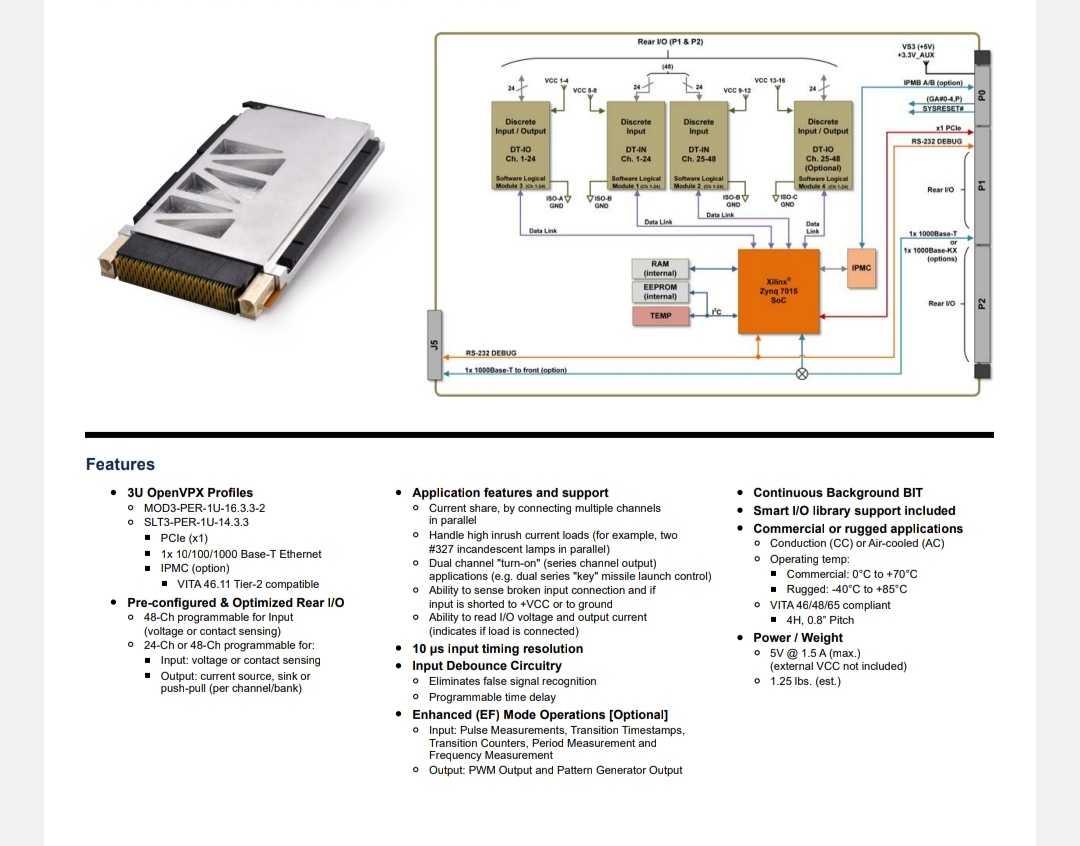
The NAI 68DT1 is a re-packaged configuration of NAI COSA® module types that provide a multifunction I/O board. It offers up to 96 channels of either ‘Standard Function’ (SF) DT1-type or ‘Enhanced Function’ (EF) DT4-type Discrete I/O function. The discrete I/O channels are mapped to 24 channels per module across four “virtual” modules within the board’s architecture:
- Software Logical Module 1: Discrete Input Channels 1-24
- Software Logical Module 2: Discrete Input Channels 25-48
- Software Logical Module 3: Discrete Input/Output Channels 1-24
- Software Logical Module 4: Discrete Input/Output Channels 25-48 (Optional)
Each channel can be configured as an input or one of three types of outputs. The I/O format (Low and High) registers are used to set each channel’s configuration.
Manual
Click the link below for the full product manual with detailed information.
The manual covers the following topics:
- Introduction: Overview of the module or board, including its purpose and applications.
- Features: Key features and functionalities.
- Specifications: Technical specifications such as dimensions, power requirements, and environmental conditions.
- Principle of Operation: Detailed explanation of how the module or board operates.
- Built-In Test (BIT) / Diagnostic Capability: Information on self-test and diagnostic features.
- Status and Interrupts: Details on status registers and interrupt handling.
- Pin-Out Details: Specifics on connector pin-outs and wiring.
- Mounting Requirements: Mechanical mounting information.
- Qualification: Information on the qualification and compliance standards
68DT1 3U OpenVPX Multifunction Discrete I/O Board
68DT1 3U OpenVPX High Density I/O Boards
3U OpenVPX Multichannel Discrete I/O Board
The 68DT1 is a 3U OpenVPX™ board featuring up to 96-Channels of Standard Functionality (SF) DT1 module-type or Enhanced Functionality (EF) DT4 module-type Discrete I/O functions [optioned, factory configurable]. 48-Channels are dedicated as input (voltage or contact sensing with programmable, pull-up/pull-down current sources). An additional 24 or 48-Channels are programmable for either input or output (current source, sink, or push-pull) switching up to 500 mA per channel from an applied 3 – 60 V external VCC source (or sink to ISO-GND). The 68DT1 has the capability to sense broken input connections and whether an input is shorted to +VCC or to ground. Additional features of the DT4 EF are listed below. The 68DT1 offers unparalleled programming flexibility, a wide range of operating characteristics, and a unique design that eliminates the need for pull-up resistors or mechanical jumpers.
abc
Architected for Versatility
NAI’s Custom-On-Standard Architecture™ (COSA®) offers a choice of over 40 Intelligent I/O, communications, or Ethernet switch functions, providing the highest packaging density and greatest flexibility of any 3U SBC in the industry. Preexisting, fully-tested functions can be combined in an unlimited number of ways quickly and easily.
Board Support Package and Software Support
The 75PPC1 includes BSP and SDK support for Wind River® VxWorks®. In addition, software support kits are supplied, with source code and board-specific library I/O APIs, to facilitate system integration. Each I/O function has dedicated processing, unburdening the SBC from unnecessary data management overhead.
Background Built-In-Test (BIT)
BIT continuously monitors the status of all I/O during normal operations and is totally transparent to the user. SBC resources are not consumed while executing BIT routines. This simplifies maintenance, assures operational readiness, reduces life-cycle costs and— keeps your systems mission ready.
One-Source Efficiencies
Eliminate man-months of integration with a configured, field-proven system from NAI. Specification to deployment is a seamless experience as all design, state-of-the-art manufacturing, assembly and test are performed— by one trusted source. All facilities are in the U.S. and optimized for high-mix/low volume production runs and extended lifecycle support.
Product Lifecycle Management
From design-in to production, and beyond, NAI’s product lifecycle management strategy ensures the long-term availability of COTS products through configuration management, technology refresh, and obsolescence component purchase and storage.
Link to original
INTRODUCTION
North Atlantic Industries (NAI) is a leading independent supplier of rugged COTS embedded computing products for industrial, commercial aerospace, and defense markets. Aligned with MOSA, SOSA and FACE standards, NAI’s Configurable Open System Architecture™ (COSA®) accelerates a customer’s time-to-mission by providing the most modular, agile, and rugged COTS portfolio of embedded smart modules, I/O boards, Single Board Computers (SBCs), Power Supplies and Ruggedized Systems of its kind. COSA products are pre-engineered to work together, enabling easy changes, reuses, or repurposing down the road. By utilizing FPGAs and SoCs, NAI has created smart modules that enable the rapid creation of configurable mission systems while reducing or eliminating SBC overhead.
NAI’s 68DT1 3U OpenVPX Multichannel Discrete I/O Board features up to 96-channels of Standard Functionality (SF) DT1 module-type (or optional Enhanced Functionality (EF) DT4 module-type) Discrete I/O functions.
68DT1 Overview
The 68DT1 3U OpenVPX Multichannel I/O Board offers a variety of features designed to meet the needs of complex requirements for integrated multifunction I/O-intensive, mission-critical applications. Some of the key features include:
3U Profiles supported:
The board is compatible with both VPX and OpenVPX Profile standards, with module and slot profiles specified as
MOD3-PER-1U-16.3.3-2
SLT3-PER-1U-14.3.3
This ensures interoperability with other components and promotes system-level integration for efficient optimized performance.
PCIe connectivity:
The 68CB6 provides one (1) x1 PCIe interface for fast and efficient data transfer. 1x 10/100/1000 Base-T:
The board provides one (1) 10/100/1000 Base-T Ethernet port to the front I/O. This port provides data communication capabilities and network connectivity for advanced control and data acquisition applications.
- IPMC support (option):*
The 68DT1 board has IPMC (Intelligent Platform Management Controller) support, which is VITA 46.11 Tier-2 compatible. This allows for advanced system monitoring and control from a host Chassis Manager.
- Pre-configured and Optimized Rear I/O*:
The board is designed with four (4) ‘virtual’ inboard modules providing up to 96 channels of Standard Function (SF) or optional Enhanced Function (EF) Discrete I/O function.
48 Channels of Discrete Input:
The 68DT1 features 48 channels dedicated to discrete input that provide the following:
Voltage or contact sensing with programmable, pull-up/pull-down current sources
24 or (optionally) 48 Channels of Discrete Input/Output:
The 68DT1 features an additional 24 or (optionally) 48 channels programmable for either discrete input or output that provide the following:
Input – voltage or contact sensing with programmable, pull-up/pull-down current sources, eliminating need for external resistors or mechanical jumpers.
Output – programmable current source (high-side), sink (low-side) or push-pull switching up to 500 mA per channel from an applied 3-60V external VCC source (or sink to ISO-GND).
- Range of Application Features and Support*:
The board is designed with a wide range of features that enable it to support a variety of functions.
Supports current share, by connecting multiple channels in parallel.
Can handle high inrush current loads, such as two #327 incandescent lamps in parallel.
Supports dual channel ‘turn-on’ (series channel output) applications. One example is dual series ‘key’ missile launch control.
Capable of sensing broken input connections and if the input is shorted to +VCC or to ground.
Able to read I/O voltage and output current and indicate if load is connected.
Input Debounce Circuitry:
The 68DT1 includes functionality that when set to input, filters out false signals by way of a programmable time delay.
Optional Enhanced Function (EF) Mode Operation:
When configured as such, the 68DT1 can utilize the following Enhanced Functionality:
Input – Pulse Measurements, Transition Timestamps, Transition Counters, Period and Frequency Measurements.
Output – Pulse Width Modulation (PWM) Output and Pattern Generator Output.
Background Built-In-Test (BIT):
The board’s BIT continually checks and reports on the health of each channel, allowing for proactive maintenance and reducing the likelihood of downtime.
Smart I/O Library Support:
The 68DT1 comes with smart I/O library support to help manage and control the I/O capabilities of the board.
Software Support Kits (SSKs) and Drivers:
SSKs and drivers are available to make the board easier to integrate into a system and develop software.
Commercial and rugged mechanical options:
The 68DT1 is available in both commercial and rugged models, making it suitable for a wide range of applications.
Operating temperature:
The board has a wide operating temperature range, with models operating from:
0° C to 70° C (commercial model)
-40° C to +85° C (rugged model)
- Mechanical design*:
The mechanical design of the 68DT1 complies with VITA 46/48/65 requirements. Offering 3U 4H/0.8” (conduction and air-cooled) pitch form factor, the board is ideal for commercial development or rugged and deployable applications.
SOFTWARE SUPPORT
The ENAIBL Software Support Kit (SSK) is supplied with all system platform based board level products. This platform’s SSK contents include html format help documentation which defines board specific library functions and their respective parameter requirements. A board specific library and its source code is provided (module level ‘C’ and header files) to facilitate function implementation independent of user operating system (O/S). Portability files are provided to identify Board Support Package (BSP) dependent functions and help port code to other common system BSPs. With the use of the provided help documentation, these libraries are easily ported to any 32-bit O/S such as RTOS or Linux.
The latest version of a board specific SSK can be downloaded from our website www.naii.com in the software downloads section. A Quick-Start Software Manual is also available for download where the SSK contents are detailed, Quick-Start Instructions provided and GUI applications are described therein. For other operating system support, contact factory.
Link to original
Specifications
General for the Motherboard
Signal Logic Level: Supports LVDS PCIe ver. 3.0 bus (x1) Power (Motherboard): +12 VDC @ <1 A (est. typical)
+3.3V_AUX @ <100 mA (typical)
Then add power for each individual moduleTemperature, Operating: “C” =0° C to +70° C, “H” =-40° C to +85° C (see part number) Storage Temperature: -55° C to +105° C Temperature Cycling: Each board is cycled from -40° C to +85° C for option “H” General size: Height: 3.94” / 100 mm (3U) Width: 1.0” / 25.4 mm (5 HP) air cooled front panel options Depth: 6.3“ / 160 mm deep Weight: 21.5 oz. (610 g) unpopulated (approx.) (convection or conduction cooled)
>> then add weight for each module (typically 1.5 oz. (42 g) each)Specifications are subject to change without notice.
Environmental
Unless otherwise specified, the following table outlines the general Environmental Specifications design guidelines for board level products of North Atlantic Industries. All our cPCI, VME and OpenVPX boards are designed for either air or conduction cooling. All boards also incorporate appropriate stiffening to ensure performance during shock and vibration but also to assure reliable operation (lower fatigue stresses) over the service life of the product.
Parameters Level 1 / Commercial-AC (Air Cooled) 2 / Rugged-AC (Air Cooled) 3 / Rugged-CC (Conduction Cooled) Temperature – Operating 0° C to 70° C, Ambient -40° C to 85° C, Ambient -40° C to 85° C, at wedge lock thermal interface Temperature - Storage -40° C to 85° C -55° C to 105° C -55° C to 105° C Humidity – Operating 0 to 95%, non-condensing 0 to 95%, non-condensing 0 to 95%, non-condensing Humidity - Storage 0 to 95%, non-condensing 0 to 95%, non-condensing 0 to 95%, non-condensing Vibration – Sine 2 g peak, 15 Hz – 2 kHz 6 g peak, 15 Hz – 2 kHz 10 g peak, 15 Hz – 2 kHz Vibration – Random .002 g /Hz, 15 Hz – 2 kHz 0.04 g /Hz, 15 Hz – 2 kHz 0.1 g /Hz, 15 Hz – 2 kHz Shock 20 g peak, half-sine, 11 ms 30 g peak, half-sine 11 ms 40 g peak, half-sine, 11 ms Low Pressure Up to 15,000 ft. Up to 50,000 ft. Up to 50,000 ft. Notes:
A. Based on sweep duration of ten minutes per axis on each of the three mutually perpendicular axes. B. Displacement limited to 0.10 D.A. from 15 to 44 Hz. C. Displacement limited to 0.436 D.A. from 15 to 21 Hz. D. 60 minutes per axis on each of the three mutually perpendicular axes. E. Per MIL-STD-810G, Method 5.14.6 Procedure I, Fig.514.6C-6 Category 7 tailored (11.65 Grms): 15 Hz – 2 kHz; ASD (PSD) at 0.04 g2/Hz between 15 Hz - 150 Hz, increasing @ 4 dB/octave from 0.04 g2/Hz to 0.1 g /Hz between 150 Hz – 300 Hz, 0.1 g2/Hz between 300 Hz - 1000 Hz, decreasing @ 6 dB/octave from 0.1 g2/Hz to 0.025 g2/Hz between 1000 Hz – 2000 Hz. Three hits per direction per axis (total of 18 hits). F. Three hits per direction per axis (total of 18 hits). G. For altitudes higher than 50,000 ft., contact NAI. H. High temperature operation requires 350 lfm minimum air flow across cover/heatsink (module dependent). I. High temperature operation requires 600 lfm minimum air flow across cover/heatsink (module dependent).
Specifications subject to change without notice
Link to original
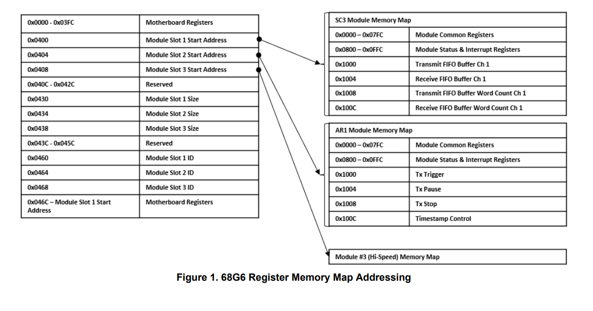
REGISTER MEMORY MAP ADDRESSING
The register map address consists of the following:
• cPCI/PCIe BAR or Base Address for the Board • Module Slot Base Address • Function Offset Address
Board Base Address
The table below lists the BAR used for access to the motherboard and module registers. The second BAR is used internally for motherboard and module firmware updates. The other cPCI/PCIe BARs not listed are not used.
NAI Boards Device ID Bus Motherboard and Module Register Access Motherboard and Module Firmware Updates Slave Boards 75G5 0x7581 cPCI BAR 0 Size: Module Dependent (minimum 64K Bytes) BAR 1 Size: 1M Bytes 79G5 0x7981 PCIe BAR 1 Size: Module Dependent (minimum 64K Bytes) BAR 2 Size: 1M Bytes 68G5/68G5P/68DT1/68CB6 0x6881 PCIe 68SDP 0x6805 PCIe 67G6 0x6781 PCIe 64G5 N/A VME Slave Window 1 Size: 8M Bytes Addressing: Geographical Addressing or DIP Switches on board. Slave Window 2 Size: 8M Bytes 74SD5 0x7405 PMC 64K Bytes N/A Controller/Master Boards 75G5/75ARM1 0x7581 cPCI BAR 0 Size: Module Dependent (minimum 64K bytes) BAR 1 Size: 1M bytes 75INT2 0x7584 cPCI BAR 1 Size: Module Dependent (minimum 64K bytes) BAR 2 Size: 1M Bytes 75PPC1 0x7584 cPCI 68ARM1 0x6884 PCIe 68ARM2 0x6886 PCIe 68PPC2 0x6884 PCIe 67PPC2 0x6784 PCIe 64ARM1 N/A VME Slave Window 1 Size: 8M Bytes Slave Window 2 Size: 8M Bytes NANO NIU1A N/A N/A Direct Memory Access Internal Direct Memory Access NIU2A N/A N/A Module Slot and Function Addresses
The memory map for the modules are dependent on the types of modules on the board and the order in which the modules are installed on the board as well as the firmware installed on the motherboard. The function modules are enumerated allowing for dynamic memory space allocation and therefore the “start” address of the module function register area is factory pre-defined (and read from) the Module Address register. Refer to Figure 1 for an example.
Motherboard Registers:
Read/Write access to the motherboard registers starts with the base address for the board and then the motherboard base offset address.
For example, to address Module Slot 1 Start Address register (i.e. register address = 0x0400):
- Start with the base address for the board.
- Add the motherbase register address offset.
Motherboard Address = Base Address
Motherboard Address Offset= 0x0000 0400 0x0000 0000 + 0x0400 Module Registers:
Read/Write access to the Function module’s registers start with the base address of the board. Add the “content” for the Module Start Address and then, add the specific module function register offset.
For example, to address an appropriate/specific function module with a register offset:
- Start with the base address for the board.
- Add the value (contents) from the module base address offset register (contents/value of Motherboard Memory register for Module 1 (i.e., @ 0x0400) = 0x4000.
- Then add the specific module function Register Offset of interest (i.e., A/D Reading Ch 1 @ 0x1000)
Link to original
(Function Specific) Address = Base Address + Module Base Address Offset + Function Register Offset = 0x0000 5000 0x0000 0000 0x4000 0x1000
MOTHERBOARD REGISTER DESCRIPTIONS
Module Information Registers
The Module Slot Addressing Ready, Module Slot Address, Module Slot Size and Module Slot ID registers provide information about the modules detected on the board.
Module Slot Addressing Ready
Link to original
Function: Indicates that the module slots are ready to be addressed. Type: unsigned binary word (32-bit) Data Range: 0x0000 0000 to 0xFFFF FFFF Read/Write: R Initialized Value: 0xA5A5A5A5 Operational Settings: This register will contain the value of 0xA5A5A5A5 when the module addresses have been determined.
Link to original
Module Slot Address Function: Specifies the Base Address for the module in the specific slot position. Type: unsigned binary word (32-bit) Data Range: 0x0000 0000 to 0xFFFF FFFF Read/Write: R Initialized Value: Based on board's module configuration. Operational Settings: 0x0000 0000 indicates no Module found.
Link to original
Module Slot Size Function: Specifies the Memory Size (in bytes) allocated for the module in the specific slot position. Type: unsigned binary word (32-bit) Range: 0x0000 0000 to 0xFFFF FFFF Read/Write: R Initialized Value: Assigned by factory for the module. Operational Settings: 0x0000 0000 indicates no Module found.
Module Slot ID Function: Specifies the Model ID for the module in the specified slot position. Type: 4-character ASCII string Data Range: 0x0000 0000 to 0xFFFF FFFF Read/Write: R Initialized Value: Assigned by factory for the module. Operational Settings: The Module ID is formatted as four ASCII bytes: three characters followed by a space. Module IDs are in little-endian order with a single space following the first three characters. For example, 'TL1' is '1LT', 'SC1' is '1CS' and so forth. Example below is for “TL1” (MSB justified). All value of 0000 0000 indicates no Module found. Link to original
D31 D30 D29 D28 D27 D26 D25 D24 D23 D22 D21 D20 D19 D18 D17 D16 ASCII Character (ex: 'T' - 0x54) ASCII Character (ex: 'L' - 0x4C) D15 D14 D13 D12 D11 D10 D9 D8 D7 D6 D5 D4 D3 D2 D1 D0 ASCII Character (ex: '1' - 0x31) ASCII Space (' ' - 0x20)
Hardware Information Registers
The registers identified in this section provide information about the board’s hardware.
Link to original
Product Serial Number Function: Specifies the Board Serial Number. Type: unsigned binary word (32-bit) Data Range: 0x0000 0000 to 0xFFFF FFFF Read/Write: R Initialized Value: Serial number assigned by factory for the board. Operational Settings: N/A
Platform
Function: Specifies the Board Platform Identifier. Values are for the ASCII characters for the NAI valid platforms (Identifiers).
Type: 4-character ASCII string
Data Range: See table below.
Read/Write: R
Initialized Value: ASCII code is for the Platform Identifier of the board
Operational Settings: NAI platform for this board is shown below:
Link to original
NAI Platform Platform Identifier ASCII Binary Values (Note: little-endian order of ascii values) 6U VME 64 0x0000 3436 6U VPX 67 0x0000 3736 3U VPX 68 0x0000 3836 3U VPX 67 0x0000 3736 ARM N/A 0x004D 5241 cPCI 75 0x0000 3537 NIU 00 0x0000 0303
Model
Function: Specifies the Board Model Identifier. Values are for the ASCII characters for the NAI valid models.
Type: unsigned binary word (32-bit)
Data Range: See table below.
Read/Write: R
Initialized Value: ASCII code is for the Model Identifier of the board
Operational Settings: Examples of NAI models and the associated values for these models are shown below:
Link to original
NAI Model ASCII Binary Values (Note: little-endian order of ascii values) ARM 0x004D 5241 G 0x0000 0047 PPC 0x0043 5050 CB 0x0000 4243 DT 0x0000 5444 INT 0x0054 4E49 NIU 0x0055 494E
Generation
Function: Specifies the Board Generation. Identifier values are for the ASCII characters for the NAI valid generation identifiers.
Type: unsigned binary word (32-bit)
Data Range: See table below.
Read/Write: R
Initialized Value: ASCII code is for the Generation Identifier of the board
Operational Settings: Examples of NAI generations and the associated values for these generations are shown below:
Link to original
NAI Generation ASCII Binary Values (Note: little-endian order of ascii values) 1 0x0000 0031 2 0x0000 0032 3E 0x0000 4533 5 0x0000 0035 6 0x0000 0036
Processor Count/Ethernet Count
Function: Specifies the Processor Count and Ethernet Count
Type: unsigned binary word (32-bit)
Data Range: See table below.
Read/Write: R
Operational Settings: Processor Count - Integer: indicates the number of unique processor types on the motherboard.
NAI Board Processor Count Description VME 64ARM1 1 Xilinx Zynq 7015 with Dual Core Cortex A9 64G5 1 Xilinx Zynq 7015 with Dual Core Cortex A9 3U-VPX 68PPC2 2 NXP QorIQ T2080 Quad-Core e6500 Processor
Xilinx Zynq 7015 with Dual Core Cortex A968ARM1 1 Xilinx Zynq 7015 with Dual Core Cortex A9 68G5 1 Xilinx Zynq 7015 68G5P 1 Xilinx Zynq 7015 68ARM2 1 Xilinx Zynq UltraScale+ Ethernet Interface Count - Indicates the number of Ethernet interfaces on the product motherboard. For example, Single Ethernet = 1; Dual Ethernet = 2.
Processor/Ethernet Interface Count
Link to original
D31 D30 D29 D28 D27 D26 D25 D24 D23 D22 D21 D20 D19 D18 D17 D16 Processor Count (See Table) D15 D14 D13 D12 D11 D10 D9 D8 D7 D6 D5 D4 D3 D2 D1 D0 Ethernet Count (Based on Part Number Ethernet Options)
Maximum Module Slot Count/ARM Platform Type
Function: Specifies the Maximum Module Slot Count and ARM Platform Type.
Type: unsigned binary word (32-bit)
Data Range: See table below.
Read/Write: R
Operational Settings:
Maximum Module Slot Count - Indicates the number of modules that can be installed on the product.
ARM Platform - Altera = 1; Xilinx X1 = 2; Xilinx X2 = 3; UltraScale = 4
NAI Board Maximum Module Slot Count ARM Platform Type VME 64ARM1 6 Xilinx X1 = 2; Xilinx X2 = 3 64G5 6 Xilinx X2 = 3 3U-VPX 68PPC2 2 Xilinx X2 = 3 68ARM1 3 Xilinx X2 = 3 68G5 3 Xilinx X1 = 2; Xilinx X2 = 3 68G5P 3 Xilinx X2 = 3 68ARM2 3 UltraScale = 4 Maximum Module Slot Count / ARM Platform Type
Link to original
D31 D30 D29 D28 D27 D26 D25 D24 D23 D22 D21 D20 D19 D18 D17 D16 Maximum Module Slot Count (See Table) D15 D14 D13 D12 D11 D10 D9 D8 D7 D6 D5 D4 D3 D2 D1 D0 ARM Platform Type (See Table)
Motherboard Firmware Information Registers
The registers in this section provide information on the revision of the firmware installed on the motherboard.
Motherboard Core (MBCore) Firmware Version Function: Specifies the Version of the NAI factory provided Motherboard Core Application installed on the board. Type: Two (2) unsigned binary word (32-bit) Data Range: 0x0000 0000 to 0xFFFF FFFF Read/Write: R Operational Settings: The motherboard firmware version consists of four components: Major, Minor, Minor 2 and Minor 3. Link to original
Motherboard Core Firmware Version (Note: little-endian order in register) (ex. 4.7.0.0) Word 1 (Ex. 0007 0004 = 4.7 (Major.Minor) D31 D30 D29 D28 D27 D26 D25 D24 D23 D22 D21 D20 D19 D18 D17 D16 Minor (ex: 0x0007 = 7) D15 D14 D13 D12 D11 D10 D9 D8 D7 D6 D5 D4 D3 D2 D1 D0 Major (ex: 0x0004 = 4) Word 2 (Ex. 0x0000 0000 = 0000 = 0.0 (Minor2.Minor3)) D31 D30 D29 D28 D27 D26 D25 D24 D23 D22 D21 D20 D19 D18 D17 D16 Minor 3 (ex: 0x000 = 0) D15 D14 D13 D12 D11 D10 D9 D8 D7 D6 D5 D4 D3 D2 D1 D0 Minor 2 (ex: 0x000 = 0)
Motherboard Firmware Build Time/Date Function: Specifies the Build Date/Time of the NAI factory provided Motherboard Core Application installed on the board. Type: Two (2) unsigned binary word (32-bit) Data Range: N/A Read/Write: R Operational Settings: The motherboard firmware time consists of the Build Date and Build Time. NOTE: On some builds the the Date/Time fields are fixed to 0000 0000 to maintain binary consistency across builds. Link to original
Motherboard Firmware Build Time (Note: little-endian order in register) Word 1 - Build Date (ex. 0x030C 07E2 = 2018-12-03) D31 D30 D29 D28 D27 D26 D25 D24 D23 D22 D21 D20 D19 D18 D17 D16 Day (ex: 0x03 = 3) Month (ex: 0x0C = 12) D15 D14 D13 D12 D11 D10 D9 D8 D7 D6 D5 D4 D3 D2 D1 D0 Year (ex: 0x07E2 = 2018) Word 2 - Build Time (ex. 0x001B 3B0A = 10:59:27) D31 D30 D29 D28 D27 D26 D25 D24 D23 D22 D21 D20 D19 D18 D17 D16 null (0x00) Seconds (ex: 0x1B = 27) D15 D14 D13 D12 D11 D10 D9 D8 D7 D6 D5 D4 D3 D2 D1 D0 Minutes (ex: 0x3B = 59) Hours (ex: 0x0A = 10)
Motherboard Monitoring Registers
The registers in this provide motherboard voltage and temperature measurement information, and where applicable the host processor and slave processor measurements.
| NAI Boards | Bus | Has Host Processor | Has Slave Processor |
|---|---|---|---|
| Slave Boards | 68DT1 | PCIe | No |
| No |
Motherboard Software Initialization Status
Function: Indicates the status of the motherboard software (MBCore) initialization.
Type: unsigned binary word (32-bit)
Data Range: 0 to 1
Read/Write: R
Initialized Value: 0
Operational Settings: Indicates whether the motherboard software initialization has not occurred (0) or has been completed (1). Any other value will indicate an error code.
Link to originalNote
This register will be available beginning with MBCore version 4.129 and OpBM version 4.503.
Zynq Core Voltage
Function: Specifies the Measured Zynq Core Voltage.
Type: unsigned word (16-bits) for integer part and unsigned word (16-bits) for fractional part
Data Range: 0x0000 0000 to 0xFFFF FFFF
Read/Write: R
Initialized Value: Value corresponding to the Measured Zynq Core Voltage (based on the conversion below)
Operational Settings: The upper 16-bits are the Integer part of the Voltage and the lower 16-bits is the Fractional part of the Voltage. For example, if the register contains the value 0x0000 03DE, this represents 0.990 Volts.
Zynq Core Voltage
Link to original
D31 D30 D29 D28 D27 D26 D25 D24 D23 D22 D21 D20 D19 D18 D17 D16 Integer part of Voltage D15 D14 D13 D12 D11 D10 D9 D8 D7 D6 D5 D4 D3 D2 D1 D0 Fractional part of Voltage
Zynq Aux Voltage
Function: Specifies the Measured Zynq Aux Voltage.
Type: unsigned word (16-bits) for integer part and unsigned word (16-bits) for fractional part
Data Range: 0x0000 0000 to 0xFFFF FFFF
Read/Write: R
Initialized Value: Value corresponding to the Measured Zynq Aux Voltage (based on the conversion below)
Operational Settings: The upper 16-bits are the Integer part of the Voltage and the lower 16-bits is the Fractional part of the Voltage. For example, if the register contains the value 0x0001 0315, this represents 1.789 Volts.
Zynq Aux Voltage
Link to original
D31 D30 D29 D28 D27 D26 D25 D24 D23 D22 D21 D20 D19 D18 D17 D16 Integer part of Voltage D15 D14 D13 D12 D11 D10 D9 D8 D7 D6 D5 D4 D3 D2 D1 D0 Fractional part of Voltage
Zynq DDR Voltage
Function: Specifies the Measured Zynq DDR Voltage.
Type: unsigned word (16-bits) for integer part and unsigned word (16-bits) for fractional part
Data Range: 0x0000 0000 to 0xFFFF FFFF
Read/Write: R
Initialized Value: Value corresponding to the Measured Zynq DDR Voltage (based on the conversion below)
Operational Settings: The upper 16-bits are the Integer part of the Voltage and the lower 16-bits is the Fractional part of the Voltage. For example, if the register contains the value 0x0001 00C5, this represents 1.197 Volts.
Zynq DDR Voltage
Link to original
D31 D30 D29 D28 D27 D26 D25 D24 D23 D22 D21 D20 D19 D18 D17 D16 Integer part of Voltage D15 D14 D13 D12 D11 D10 D9 D8 D7 D6 D5 D4 D3 D2 D1 D0 Fractional part of Voltage
Temperature Readings Register
The temperature registers provide the current, maximum (from power-up) and minimum (from power-up) for the processor and PCB for Zynq processor, and Host and Slave processors measurements for boards that have these additional processors (Refer to Motherboard Monitoring Registers table).
Function: Specifies the Measured Temperatures on Motherboard.
Type: signed byte (8-bits) for each temperature reading – Six (6) 32-bit words
Data Range: 0x0000 0000 to 0x0000 FFFF
Read/Write: R
Initialized Value: Value corresponding to the measured temperatures based on the table below.
Word 3 (Max Zynq Temperatures)
Operational Settings: The 8-bit temperature readings are signed bytes. For example, if the following register contains the value 0x0000 5569:
Example:
Word 3 (Max Zynq Temperatures)
| D31 | D30 | D29 | D28 | D27 | D26 | D25 | D24 | D23 | D22 | D21 | D20 | D19 | D18 | D17 | D16 |
|---|---|---|---|---|---|---|---|---|---|---|---|---|---|---|---|
| 0x00 | 0x00 | D15 | D14 | D13 | D12 | D11 | D10 | D9 | D8 | D7 | D6 | D5 | D4 | D3 | D2 |
| D1 | D0 | Max Zynq PCB Temperature | Max Zynq Core Temperature |
The values would represent the following temperatures:
| Temperature Measurements | Data Bits | Value | Temperature (Celsius) |
|---|---|---|---|
| Max Zynq PCB Temperature | D15:D8 | 0x55 | +85° |
| Max Zynq Core Temperature | D7:D0 | 0x69 | +105° |
Temperature Readings
Word 1 (Current Zynq Temperatures)
| D31 | D30 | D29 | D28 | D27 | D26 | D25 | D24 | D23 | D22 | D21 | D20 | D19 | D18 | D17 | D16 |
|---|---|---|---|---|---|---|---|---|---|---|---|---|---|---|---|
| Zynq Core Temperature | Zynq PCB Temperature | D15 | D14 | D13 | D12 | D11 | D10 | D9 | D8 | D7 | D6 | D5 | D4 | D3 | D2 |
| D1 | D0 | 0x00 | 0x00 Word 2 (Reserved) | D31 | D30 | D29 | D28 | D27 | D26 | D25 | D24 | D23 | D22 | D21 | D20 |
| D19 | D18 | D17 | D16 | 0x00 | 0x00 | D15 | D14 | D13 | D12 | D11 | D10 | D9 | D8 | D7 | D6 |
| D5 | D4 | D3 | D2 | D1 | D0 | 0x00 | 0x00 Word 3 (Max Zynq Temperatures) | D31 | D30 | D29 | D28 | D27 | D26 | D25 | D24 |
| D23 | D22 | D21 | D20 | D19 | D18 | D17 | D16 | Zynq Core Max Temp | Zynq PCB Max Temp | D15 | D14 | D13 | D12 | D11 | D10 |
| D9 | D8 | D7 | D6 | D5 | D4 | D3 | D2 | D1 | D0 | 0x00 | 0x00 Word 4 (Reserved) | D31 | D30 | D29 | D28 |
| D27 | D26 | D25 | D24 | D23 | D22 | D21 | D20 | D19 | D18 | D17 | D16 | 0 | 0 | 0 | 0 |
| 0 | 0 | 0 | 0 | 0 | 0 | 0 | 0 | 0 | 0 | 0 | 0 | D15 | D14 | D13 | D12 |
| D11 | D10 | D9 | D8 | D7 | D6 | D5 | D4 | D3 | D2 | D1 | D0 | 0x00 | 0x00 Word 5 (Min Zynq Temperatures) | D31 | D30 |
| D29 | D28 | D27 | D26 | D25 | D24 | D23 | D22 | D21 | D20 | D19 | D18 | D17 | D16 | 0 | 0 |
| 0 | 0 | 0 | 0 | 0 | 0 | 0 | 0 | 0 | 0 | 0 | 0 | 0 | 0 | D15 | D14 |
| D13 | D12 | D11 | D10 | D9 | D8 | D7 | D6 | D5 | D4 | D3 | D2 | D1 | D0 | Min Zynq Core Temperature | Min Zynq PCB Temperature Word 6 (Reserved) |
| D31 | D30 | D29 | D28 | D27 | D26 | D25 | D24 | D23 | D22 | D21 | D20 | D19 | D18 | D17 | D16 |
| 0 | 0 | 0 | 0 | 0 | 0 | 0 | 0 | 0 | 0 | 0 | 0 | 0 | 0 | 0 | 0 |
| D15 | D14 | D13 | D12 | D11 | D10 | D9 | D8 | D7 | D6 | D5 | D4 | D3 | D2 | D1 | D0 |
| 0x00 | 0x00 |
Higher Precision Temperature Readings Register
These registers provide higher precision readings of the current Zynq and PCB temperatures.
Higher Precision Zynq Core Temperature Function: Specifies the Higher Precision Measured Zynq Core temperature on Interface Board. Type: signed word (16-bits) for integer part and unsigned word (16-bits) for fractional part Data Range: 0x0000 0000 to 0xFFFF FFFF Read/Write: R Initialized Value: Measured Zynq Core temperature on Interface Board Operational Settings: The upper 16-bits represent the signed integer part of the temperature and the lower 16-bits represent the fractional part of the temperature with the resolution of 1/1000 of degree Celsius. For example, if the register contains the value 0x002B 0271, this represents Zynq Core Temperature = 43.625° Celsius, and value 0xFFF6 0177 represents -10.375° Celsius. Link to original
D31 D30 D29 D28 D27 D26 D25 D24 D23 D22 D21 D20 D19 D18 D17 D16 Signed Integer Part of Temperature D15 D14 D13 D12 D11 D10 D9 D8 D7 D6 D5 D4 D3 D2 D1 D0 Fractional Part of Temperature
Higher Precision Motherboard PCB Temperature Function: Specifies the Higher Precision Measured Motherboard PCB temperature. Type: signed word (16-bits) for integer part and unsigned word (16-bits) for fractional part Data Range: 0x0000 0000 to 0xFFFF FFFF Read/Write: R Initialized Value: Measured Motherboard PCB temperature Operational Settings: The upper 16-bits represent the signed integer part of the temperature and the lower 16-bits represent the fractional part of the temperature with the resolution of 1/1000 of degree Celsius. For example, if the register contains the value 0x0020 007D, this represents Interface PCB Temperature = 32.125° Celsius, and value 0xFFE8 036B represents -24.875° Celsius. Link to original
D31 D30 D29 D28 D27 D26 D25 D24 D23 D22 D21 D20 D19 D18 D17 D16 Signed Integer Part of Temperature D15 D14 D13 D12 D11 D10 D9 D8 D7 D6 D5 D4 D3 D2 D1 D0 Fractional Part of Temperature
Ethernet Configuration Registers
The registers in this section provide information about the Ethernet Configuration for the two ports on the board.
Important: Regardless if the board is configured for one or two Ethernet ports, the second IP address cannot be on the same Subnet as the First IP Address. The table below provides examples of valid and invalid IP Addresses and Subnet Mask Addresses.
Link to original
First Port (A) IP Address First Port (A) Subnet Mask Second Port (B) IP Address Second Port (B) Subnet Mask Result 192.168.1.5 255.255.255.0 192.168.2.5 255.255.255.0 Good 192.168.1.5 255.255.0.0 192.168.2.5 255.255.0.0 Conflict 192.168.1.5 255.255.0.0 192.168.2.5 255.255.255.0 Conflict 10.0.0.15 255.0.0.0 192.168.1.5 255.255.255.0 Good
Ethernet MAC Address and Ethernet Settings Function: Specifies the Ethernet MAC Address and Ethernet Settings for the Ethernet port. Type: Two (2) unsigned binary word (32-bit) Data Range: See table. Read/Write: R Operational Settings: The Ethernet MAC Address consists of six octets. The Ethernet Settings are defined in table.
Bits Description Values D31:D23 Reserved 0 D22:D21 Duplex 00 = Not Specified, ` 01 = Half Duplex, ` 10 = Full Duplex, + 11 = Reserved D20:D18 Speed 000 = Not Specified, ` 001 = 10 Mbps, ` 010 = 100 Mbps, ` 011 = 1000 Mbps, ` 100 = 2500 Mbps, ` 101 = 10000 Mbps, ` 110 = Reserved, + 111 = Reserved D17 Auto Negotiate 0 = Enabled, + 1 = Disabled D16 Static IP Address 0 = Enabled, + 1 = Disabled Link to original
Ethernet MAC Address and Ethernet Settings (Note: little-endian order in register) Word 1 (Ethernet MAC Address (Octets 1-4)) (ex: aa:bb:cc:dd:ee:ff) D31 D30 D29 D28 D27 D26 D25 D24 D23 D22 D21 D20 D19 D18 D17 D16 MAC Address Octet 4 (ex: 0xDD) MAC Address Octet 3 (ex: 0xCC) D15 D14 D13 D12 D11 D10 D9 D8 D7 D6 D5 D4 D3 D2 D1 D0 MAC Address Octet 2 (ex: 0xBB) MAC Address Octet 1 (ex: 0xAA) Word 2 (Ethernet MAC Address (Octets 5-6) and Ethernet Settings) D31 D30 D29 D28 D27 D26 D25 D24 D23 D22 D21 D20 D19 D18 D17 D16 Ethernet Settings (See table) D15 D14 D13 D12 D11 D10 D9 D8 D7 D6 D5 D4 D3 D2 D1 D0 MAC Address Octet 6 (ex: 0xFF) MAC Address Octet 5 (ex: 0xEE)
Ethernet Interface Name Function: Specifies the Ethernet Interface Name for the Ethernet port. Type: 8-character ASCII string Data Range: See table. Read/Write: R Operational Settings: The Ethernet Interface Name (eth0, eth1, etc) for the Ethernet port. Link to original
Ethernet Interface Name (Note: ascii string in register) (ex. “eth0”) Word 1 (Bit 0-31) (ex: 0x3068 7465 = “0hte”) D31 D30 D29 D28 D27 D26 D25 D24 D23 D22 D21 D20 D19 D18 D17 D16 ASCII Character (ex: '0' - 0x30) ASCII Character (ex: 'h' - 0x68) D15 D14 D13 D12 D11 D10 D9 D8 D7 D6 D5 D4 D3 D2 D1 D0 ASCII Character (ex: 't' - 0x74) ASCII Character (ex: 'e' - 0x65) Word 2 (Bit 32-63) (ex: 0x0000 0000) D31 D30 D29 D28 D27 D26 D25 D24 D23 D22 D21 D20 D19 D18 D17 D16 ASCII Character (ex: null - 0x00) ASCII Character (ex: null - 0x00) D15 D14 D13 D12 D11 D10 D9 D8 D7 D6 D5 D4 D3 D2 D1 D0 ASCII Character (ex: null - 0x00) ASCII Character (ex: null - 0x00)
Ethernet IPv4 Address Function: Specifies the Ethernet IPv4 Address for the Ethernet port. Type: Three (3) unsigned binary word (32-bit) Data Range: See table. Read/Write: R Operational Settings: The Ethernet IPv4 Address consists of three parts: IPv4 Address, IPv4 Subnet Mask and IPv4 Gateway. Link to original
Ethernet IPv4 Address (Note: little-endian order in register) Word 1 (Ethernet IPv4 Address) (ex: 0x1001 A8C0 = 192.168.1.16) D31 D30 D29 D28 D27 D26 D25 D24 D23 D22 D21 D20 D19 D18 D17 D16 IPv4 Address Octet 4 (ex: 0x10 = 16) IPv4 Address Octet 3 (ex: 0x01 = 1) D15 D14 D13 D12 D11 D10 D9 D8 D7 D6 D5 D4 D3 D2 D1 D0 IPv4 Address Octet 2 (ex: 0xA8 = 168) IPv4 Address Octet 1 (ex: 0xC0 = 192) Word 2 (Ethernet IPv4 Subnet) (ex: 0x00FF FFFF = 255.255.255.0) D31 D30 D29 D28 D27 D26 D25 D24 D23 D22 D21 D20 D19 D18 D17 D16 IPv4 Subnet Octet 4 (ex: 0x00 = 0) IPv4 Subnet Octet 3 (ex: 0xFF = 255) D15 D14 D13 D12 D11 D10 D9 D8 D7 D6 D5 D4 D3 D2 D1 D0 IPv4 Subnet Octet 2 (ex: 0xFF = 255) IPv4 Subnet Octet 1 (ex: 0xFF = 255) Word 3 (Ethernet IPv4 Gateway) (ex: 0x0101 A8C0 = 192.168.1.1) D31 D30 D29 D28 D27 D26 D25 D24 D23 D22 D21 D20 D19 D18 D17 D16 IPv4 Gateway Octet 4 (ex: 0x01 = 1) IPv4 Gateway Octet 3 (ex: 0x01 = 1) D15 D14 D13 D12 D11 D10 D9 D8 D7 D6 D5 D4 D3 D2 D1 D0 IPv4 Gateway Octet 2 (ex: 0xA8 = 168) IPv4 Gateway Octet 1 (ex: 0xC0 = 192)
Ethernet IPv6 Address Function: Specifies the Ethernet IPv6 Address for the Ethernet port. Type: Five (5) unsigned binary word (32-bit) Data Range: See table. Read/Write: R Operational Settings: The IPv6 Prefix length indicates the network portion of an IPv6 address using the following format: IPv6 address/prefix length ` Prefix length can range from 0 to 128 ` * Typical prefix length is 64 The following is an illustration of IPv6 addressing with IPv6 Prefix length of 64.
64 bits 64 bits Prefix Interface ID Prefix 1 Prefix 2 Prefix 3 Subnet ID Interface ID 1 Interface ID 2 Interface ID 3 Interface ID 4 Example: 2002:c0a8:101:0:7c99:d118:9058:1235/64 2002 C0A8 0101 0000 7C99 D118 9058 1235 Link to original
Ethernet IPv6 Address (Note: little-endian order within 32-bit and 16-bit words in register) (ex. IPv6 Address: 2002:c0a8:201:0:7c99:d118:9058:1235 IPv6 Prefix: 64) Word 1 (Ethernet IPv6 Address (Prefix 1-2)) (ex:0xA8C0 0220 = 2002 C0A8) D31 D30 D29 D28 D27 D26 D25 D24 D23 D22 D21 D20 D19 D18 D17 D16 Prefix 2 (ex: 0xA8C0 = C0A8) D15 D14 D13 D12 D11 D10 D9 D8 D7 D6 D5 D4 D3 D2 D1 D0 Prefix 1 (ex: 0x0220 = 2002) Word 2 (Ethernet IPv6 Address (Prefix 3/Subnet ID)) + (ex:0x000 0101 = 0101 0000) D31 D30 D29 D28 D27 D26 D25 D24 D23 D22 D21 D20 D19 D18 D17 D16 Subnet ID (ex: 0x0000 = 0000) D15 D14 D13 D12 D11 D10 D9 D8 D7 D6 D5 D4 D3 D2 D1 D0 Prefix 3 (ex: 0x0101 = 0101) Word 3 (Ethernet IPv6 Address (Interface ID 1-2)) + (ex: 0x18D1 997C = 7C99 D118) D31 D30 D29 D28 D27 D26 D25 D24 D23 D22 D21 D20 D19 D18 D17 D16 Interface ID 2 (ex: 0x18D1 = D118) D15 D14 D13 D12 D11 D10 D9 D8 D7 D6 D5 D4 D3 D2 D1 D0 Interface ID 1 (ex: 0x997C = 7C99) Word 4 (Ethernet IPv6 Address (Interface ID 3-4)) + (ex: 0x3512 5890 = 9058 1235) D31 D30 D29 D28 D27 D26 D25 D24 D23 D22 D21 D20 D19 D18 D17 D16 Interface ID 4 (ex: 0x3512 = 1235) D15 D14 D13 D12 D11 D10 D9 D8 D7 D6 D5 D4 D3 D2 D1 D0 Interface ID 3 (ex: 0x5890 = 9058) Word 5 (Ethernet IPv6 Prefix Length) + (ex:0x0000 0040) D31 D30 D29 D28 D27 D26 D25 D24 D23 D22 D21 D20 D19 D18 D17 D16 0 0 0 0 0 0 0 0 0 0 0 0 0 0 0 0 D15 D14 D13 D12 D11 D10 D9 D8 D7 D6 D5 D4 D3 D2 D1 D0 Prefix Length (ex: 0x0040 = 64)
Interrupt Vector and Steering
When interrupts are enabled, the interrupt vector associated with the specific interrupt can be programmed (typically with a unique number/identifier) such that it can be utilized in the Interrupt Service Routine (ISR) to identify the type of interrupt. When an interrupt occurs, the contents of the Interrupt Vector registers is reported as part of the interrupt mechanism. In addition to specifying the interrupt vector, the interrupt can be directed (“steered”) to the native bus or to the application running on the onboard ARM processor.
Note
The Interrupt Vector and Interrupt Steering registers are mapped to the Motherboard Common Memory and these registers are associated with the Module Slot position (refer to Function Register Map).
Interrupt Vector Function: Set an identifier for the interrupt. Type: unsigned binary word (32-bit) Data Range: 0x0000 0000 to 0xFFFF FFFF Read/Write: R/W Initialized Value: 0 Operational Settings: When an interrupt occurs, this value is reported as part of the interrupt mechanism.
Interrupt Steering Function: Sets where to direct the interrupt. Type: unsigned binary word (32-bit) Data Range: See table Read/Write: R/W Initialized Value: 0 Operational Settings: When an interrupt occurs, the interrupt is sent as specified: Link to original
Direct Interrupt to VME 1 Direct Interrupt to ARM Processor (via SerDes) +
(Custom App on ARM or NAI Ethernet Listener App)2 Direct Interrupt to PCIe Bus 5 Direct Interrupt to cPCI Bus 6
Motherboard Health Monitoring Registers
The registers in this section provide motherboard voltage, current and temperature measurement information.
Motherboard Sensor Summary Alarm Function: The corresponding sensor bit is set if the sensor has crossed any of its thresholds. Type: unsigned binary word (32-bits) Data Range: See table below Read/Write: R Initialized Value: 0 Operational Settings: This register provides a summary for motherboard sensors. When the corresponding sensor bit is set, the Sensor Threshold Status register for that sensor will indicate the threshold condition that triggered the event. Link to original
Bit(s) Sensor D31:D5 Reserved D4 Motherboard PCB Temperature D3 Zynq Core Temperature D2:D0 Reserved
Motherboard Sensor Status
The registers listed in this section apply to each module sensor listed for the Motherboard Sensor Summary Status register.
Sensor Threshold Status Function: Reflects which threshold has been crossed Type: unsigned binary word (32-bits) Data Range: See table below Read/Write: R Initialized Value: 0 Operational Settings: The associated bit is set when the sensor reading exceed the corresponding threshold settings. Link to original
Bit(s) Description D31:D4 Reserved D3 Exceeded Upper Critical Threshold D2 Exceeded Upper Warning Threshold D1 Exceeded Lower Critical Threshold D0 Exceeded Lower Warning Threshold
Link to original
Sensor Current Reading Function: Reflects current reading of temperature sensor Type: Single Precision Floating Point Value (IEEE-754) Data Range: Single Precision Floating Point Value (IEEE-754) Read/Write: R Initialized Value: N/A Operational Settings: The register represents current sensor reading as a single precision floating point value. For example, for a temperature sensor, register value 0x41C6 0000 represents temperature = 24.75° Celsius.
Link to original
Sensor Minimum Reading Function: Reflects minimum value of temperature sensor since power up Type: Single Precision Floating Point Value (IEEE-754) Data Range: Single Precision Floating Point Value (IEEE-754) Read/Write: R Initialized Value: N/A Operational Settings: The register represents minimum sensor value as a single precision floating point value. For example, for a temperature sensor, register value 0x41C6 0000 represents temperature = 24.75° Celsius.
Link to original
Sensor Maximum Reading Function: Reflects maximum value of temperature sensor since power up Type: Single Precision Floating Point Value (IEEE-754) Data Range: Single Precision Floating Point Value (IEEE-754) Read/Write: R Initialized Value: N/A Operational Settings: The register represents maximum sensor value as a single precision floating point value. For example, for a temperature sensor, register value 0x41C6 0000 represents temperature = 24.75° Celsius.
Link to original
Sensor Lower Warning Threshold Function: Reflects lower warning threshold of temperature sensor Type: Single Precision Floating Point Value (IEEE-754) Data Range: Single Precision Floating Point Value (IEEE-754) Read/Write: R/W Initialized Value: Default lower warning threshold (value dependent on specific sensor) Operational Settings: The register represents sensor lower warning threshold as a single precision floating point value. For example, for a temperature sensor, register value 0xC220 0000 represents temperature = -40.0° Celsius.
Link to original
Sensor Lower Critical Threshold Function: Reflects lower critical threshold of temperature sensor Type: Single Precision Floating Point Value (IEEE-754) Data Range: Single Precision Floating Point Value (IEEE-754) Read/Write: R/W Initialized Value: Default lower critical threshold (value dependent on specific sensor) Operational Settings: The register represents sensor lower critical threshold as a single precision floating point value. For example, for a temperature sensor, register value 0xC25C 0000 represents temperature = -55.0° Celsius.
Link to original
Sensor Upper Warning Threshold Function: Reflects upper warning threshold of temperature sensor Type: Single Precision Floating Point Value (IEEE-754) Data Range: Single Precision Floating Point Value (IEEE-754) Read/Write: R/W Initialized Value: Default upper warning threshold (value dependent on specific sensor) Operational Settings: The register represents sensor upper warning threshold as a single precision floating point value. For example, for a temperature sensor, register value 0x42AA 0000 represents temperature = 85.0° Celsius.
Link to original
Sensor Upper Critical Threshold Function: Reflects upper critical threshold of temperature sensor Type: Single Precision Floating Point Value (IEEE-754) Data Range: Single Precision Floating Point Value (IEEE-754) Read/Write: R/W Initialized Value: Default upper critical threshold (value dependent on specific sensor) Operational Settings: The register represents sensor upper critical threshold as a single precision floating point value. For example, for a temperature sensor, register value 0x42FA 0000 represents temperature = 125.0° Celsius.
Modules Health Monitoring
Module Communications Status Function: Provides the ability to monitor factors may effect communication status of a Module. Type: unsigned binary word (32-bit) Data Range: 0x0000 0000 to 0xFFFF FFFF Read/Write: R Operational Settings: The Module Communications registers provide the ability to monitor factors that may effect the Communications Status of individual Modules. There is one register per Module. Each communication factor is bit mapped to the register as shown in the table below:
Bit(s) Description D31:D5 Reserved D4 Module Communications Error Detected D3 Module Firmware Not Ready D2 Module LinkInit Not Done D1 Module Not Detected D0 Module Powered-down Module Powered-down: The user can request an individual Module be powered-down (see Module Control Command Requests). Once the request is detected and acted upon, this bit will be set. Once powered-down, you will not be able to communicate with the Module.
Module Not Detected: If a Module in this slot has not been detected, you will not be able to communicate with the Module.
Module LinkInit Not Done: Module communications is accomplished via SERDES. LinkInit is required to establish a connection to the Module. If the LinkInit has not been successfully completed, you will not be able to communicate with the Module.
Module Firmware Not Ready: Each Module has Firmware that is ready from Module QSPI and loaded for execution. If this Firmware was not loaded and started successfully, you may not be able to communicate with the Module.
Module Communications Error Detected: If at some point during run-time, communications with the Module has failed, this bit will be set.
Link to original
Module BIT Status
Function: Provides the ability to monitor the individual Module BIT Status.
Type: unsigned binary word (32-bit)
Data Range: 0x0000 0000 to 0xFFFF FFFF
Read/Write: R
Operational Settings: The Module BIT Status registers provide the ability to monitor individual Module BIT results as Latched and current value. A 1 in any bit field indicates BIT failure for the Module in that slot.
Module BIT Status
Link to original
Bit(s) Description D31:21 Reserved D20 Module Slot 4 BIT Failure (current value) D19 Module Slot 3 BIT Failure (current value) D18 Module Slot 2 BIT Failure (current value) D17 Module Slot 1 BIT Failure (current value) D16 Reserved D5-D15 Reserved D4 Module Slot 4 BIT Failure – Latched D3 Module Slot 3 BIT Failure – Latched D2 Module Slot 2 BIT Failure - Latched D1 Module Slot 1 BIT Failure - Latched D0 Reserved
Scratchpad Area
Link to original
Scratchpad Area Function: Registers reserved as scratch pad for customer use. Type: unsigned binary word (32-bit) Data Range: 0x0000 0000 to 0xFFFF FFFF Read/Write: R/W Operational Settings: This area in memory is reserved for customer use.
MOTHERBOARD FUNCTION REGISTER MAP
Key: Bold Underline = Measurement/Status/Board Information
Bold Italic = Configuration/Control
Module Information Registers
| 0x03FC | Module Slot Addressing Ready | R |
|---|
| 0x0400 | Module Slot 1 Address | R |
|---|---|---|
| 0x0404 | Module Slot 2 Address | R |
| 0x0408 | Module Slot 3 Address | R |
| 0x040C | Module Slot 4 Address | R |
| 0x0430 | Module Slot 1 Size | R |
|---|---|---|
| 0x0434 | Module Slot 2 Size | R |
| 0x0438 | Module Slot 3 Size | R |
| 0x043C | Module Slot 4 Size | R |
| 0x0460 | Module Slot 1 ID | R |
|---|---|---|
| 0x0464 | Module Slot 2 ID | R |
| 0x0468 | Module Slot 3 ID | R |
| 0x046C | Module Slot 4 ID | R |
Hardware Information Registers
| 0x0020 | Product Serial Number | R |
|---|
| 0x0024 | Platform | R |
|---|---|---|
| 0x0028 | Model | R |
| 0x002C | Generation | R |
| 0x0030 | Processor Count/Ethernet Count | R |
|---|---|---|
| 0x0034 | Maximum Module Slot Count/ARM Platform Type | R |
Motherboard Firmware Information Registers
| 0x0100 | MBCore Major/Minor Version | R |
|---|---|---|
| 0x0104 | MBCore Minor 2/3 Version | R |
| 0x0108 | MBCore Build Date | R |
Motherboard Measurement Registers
| 0x0124 | MB SW Init Status | R |
|---|---|---|
| 0x0218 | Zynq Core Voltage | R |
| 0x021C | Zynq Aux Voltage | R |
| 0x0220 | Zynq DDR Voltage | R |
Temperature Readings
| 0x0200 | Current Zynq Temperatures | R |
|---|---|---|
| 0x0204 | Reserved | R |
| 0x0208 | Max Zynq Temperatures | R |
| 0x020C | Reserved | R |
| 0x0210 | Min Zynq Temperatures | R |
| 0x0214 | Reserved | R |
Higher Precision Temperature Readings
| 0x0230 | Current Zynq Core Temperature | R |
|---|---|---|
| 0x0234 | Current Motherboard PCB Temperture | R |
Ethernet Configuration Registers
| 0x0070 | Ethernet A MAC (Octets 1-4) | R |
|---|---|---|
| 0x0074 | Ethernet A MAC (Octets 5-6)/Misc Settings | R |
| 0x0078 | Ethernet A Interface Name (Bit 0-31) | R |
|---|---|---|
| 0x007C | Ethernet A Interface Name (Bit 32-63) | R |
| 0x0080 | Ethernet A IPv4 Address | R |
|---|---|---|
| 0x0084 | Ethernet A IPv4 Subnet Mask | R |
| 0x0088 | Ethernet A IPv4 Gateway | R |
| 0x008C | Ethernet A IPv6 Address (Prefix 1-2) | R |
|---|---|---|
| 0x0090 | Ethernet A IPv6 Address (Prefix 3/Subnet ID) | R |
| 0x0094 | Ethernet A IPv6 Address (Interface ID 1-2) | R |
| 0x0098 | Ethernet A IPv6 Address (Interface ID 3-4) | R |
| 0x009C | Ethernet A IPv6 Prefix Length | R |
| 0x00A0 | Ethernet B MAC (Octets 1-4) | R |
|---|---|---|
| 0x00A4 | Ethernet B MAC (Octets 5-6)/Misc Settings | R |
| 0x00A8 | Ethernet B Interface Name (Bit 0-31) | R |
|---|---|---|
| 0x00AC | Ethernet B Interface Name (Bit 32-63) | R |
| 0x00B0 | Ethernet B IPv4 Address | R |
|---|---|---|
| 0x00B4 | Ethernet B IPv4 Subnet Mask | R |
| 0x00B8 | Ethernet B IPv4 Gateway | R |
| 0x00BC | Ethernet B IPv6 Address (Prefix 1-2) | R |
|---|---|---|
| 0x00C0 | Ethernet B IPv6 Address (Prefix 3/Subnet ID) | R |
| 0x00C4 | Ethernet B IPv6 Address (Interface ID 1-2) | R |
| 0x00C8 | Ethernet B IPv6 Address (Interface ID 3-4) | R |
| 0x00CC | Ethernet B IPv6 Prefix Length | R |
Interrupt Vector and Steering
| 0x0500- 0x057C | Module 1 Interrupt Vector 1-32 | R/W |
|---|---|---|
| 0x0700- 0x077C | Module 2 Interrupt Vector 1-32 | R/W |
| 0x0900- 0x097C | Module 3 Interrupt Vector 1-32 | R/W |
| 0x0B00- 0xB97C | Module 4 Interrupt Vector 1-32 | R/W |
| 0x0600- 0x067C | Module 1 Interrupt Steering 1-32 | R/W |
|---|---|---|
| 0x0800- 0x087C | Module 2 Interrupt Steering 1-32 | R/W |
| 0x0A00- 0x0A7C | Module 3 Interrupt Steering 1-32 | R/W |
| 0x0C00- 0x0C7C | Module 4 Interrupt Steering 1-32 | R/W |
Motherboard Health Monitoring Registers
| 0x20F8 | Motherboard Sensor Summary Status 1 | R |
|---|
| 0x3800- 0x3BFF | Scratchpad Registers | R |
|---|
Modules Health Monitoring
Module Communications Status
| 0x01B8 | Module Slot 1 Communications Status | R |
|---|---|---|
| 0x01BC | Module Slot 2 Communications Status | R |
| 0x01C0 | Module Slot 3 Communications Status | R |
| 0x01C4 | Module Slot 4 Communications Status | R |
Module BIT Status
| 0x0128 | Module BIT Status (current and latched) | R |
|---|
Scratchpad Area
SPECIFIC FUNCTION OVERVIEW
The 68DT1 is a unique configuration of re-packaged NAI COSA® module types embedded and accessed as “inboard” functions. The following sections describe the register descriptions and register memory map for each of these specific functions.
The 68DT1 provides up to 96 channels of either ‘Standard Function’ (SF) DT1-type or ‘Enhanced Function’ (EF) DT4-type Discrete I/O function. 24 channels of Discrete Input or Input Output are mapped to each of four “virtual” modules that comprise the “inboard’ functionality.
The channels are mapped as follows:
-
Software Logical Module 1 (Ch 1-24): Discrete Input Channels 1-24
-
Software Logical Module 2 (Ch 1-24): Discrete Input Channels 25-48
-
Software Logical Module 3 (Ch 1-24): Discrete Input/Output Channels 1-24
-
Software Logical Module 4 (Ch 1-24): Discrete Input/Output Channels 25-48 (Optional)
See 68DT1 Block Diagram (page 7) for additional detail.
DISCRETE INPUT/OUTPUT REGISTER DESCRIPTIONS
The register descriptions provide the Register Name, Type, Data Range, Read or Write information, power on default initialized values, a description of the function and a data table where applicable,
Discrete Input/Output Registers
Each channel can be configured as an input or one of three types of outputs. The I/O Format (Low and High) registers are used to set each channel input/output configuration. The Write Outputs register controls the output channels to either a High (1) or Low (0) state, and the Read I/O register contains the discrete channel’s state (High (1) or Low (0)) as specified by the channel’s threshold configurations.
Input/Output Format Low (DT-I/O Ch 1-24, 25-48 only)
Function: Sets channels 1-16 as inputs or outputs. See Input/Output Format High register for channels 17-24.
Type: unsigned binary word (32-bit)
Data Range: 0x0000 0000 to 0xFFFF FFFF
Read/Write: R/W
Initialized Value: 0
Operational Settings: Write integer 0 for input; 1, 2 or 3 for specific output format.
| Integer | DH | DL | (2 bits per channel) |
|---|---|---|---|
| 0 | 0 | 0 | Input |
| 1 | 0 | 1 | Output, Low-side switched, with/without current pull up |
| 2 | 1 | 0 | Output, High-side switched, with/without current pull down |
| 3 | 1 | 1 | Output, push-pull |
Input/Output Format Low
| D31 | D30 | D29 | D28 | D27 | D26 | D25 | D24 | D23 | D22 | D21 | D20 | D19 | D18 | D17 | D16 |
|---|---|---|---|---|---|---|---|---|---|---|---|---|---|---|---|
| Ch16 | Ch15 | Ch14 | Ch13 | Ch12 | Ch11 | Ch10 | Ch9 | D15 | D14 | D13 | D12 | D11 | D10 | D9 | D8 |
| D7 | D6 | D5 | D4 | D3 | D2 | D1 | D0 | Ch8 | Ch7 | Ch6 | Ch5 | Ch4 | Ch3 | Ch2 | Ch1 |
Input/Output Format High (DT-I/O Ch 1-24, 25-48 only)
Function: Sets channels 17-24 as inputs or outputs. See Input/Output Format Low for channels 1-16.
Type: unsigned binary word (32-bit)
Data Range: 0x0000 0000 to 0x0000 FFFF
Read/Write: R/W
Initialized Value: 0
Operational Settings: Write integer 0 for input; 1, 2 or 3 for specific output format.
| Integer | DH | DL | (2 bits per channel) |
|---|---|---|---|
| 0 | 0 | 0 | Input |
| 1 | 0 | 1 | Output, Low-side switched, with/without current pull up |
| 2 | 1 0 | Output, High-side switched, with/without current pull down | 3 |
| 1 | 1 | Output, push-pull |
Input/Output Format High
| D31 | D30 | D29 | D28 | D27 | D26 | D25 | D24 | D23 | D22 | D21 | D20 | D19 | D18 | D17 | D16 |
|---|---|---|---|---|---|---|---|---|---|---|---|---|---|---|---|
| 0 | 0 | 0 | 0 | 0 | 0 | 0 | 0 | 0 | 0 | 0 | 0 | 0 | 0 | 0 | 0 |
| D15 | D14 | D13 | D12 | D11 | D10 | D9 | D8 | D7 | D6 | D5 | D4 | D3 | D2 | D1 | D0 |
| Ch24 | Ch23 | Ch22 | Ch21 | Ch20 | Ch19 | Ch18 | Ch17 |
Write Outputs (DT-I/O Ch 1-24, 25-48 only)
Function: Drives output channels High 1 or Low 0
Type: unsigned binary word (32-bit)
Data Range: 0x0000 0000 to 0x00FF FFFF
Read/Write: R/W
Initialized Value: 0
Operational Settings: Write 1 to drive output high. Write 0 to drive output low.
Write Outputs
| D31 | D30 | D29 | D28 | D27 | D26 | D25 | D24 | D23 | D22 | D21 | D20 | D19 | D18 | D17 | D16 |
|---|---|---|---|---|---|---|---|---|---|---|---|---|---|---|---|
| 0 | 0 | 0 | 0 | 0 | 0 | 0 | 0 | 0 | 0 | 0 | 0 | 0 | 0 | 0 | 0 |
| D15 | D14 | D13 | D12 | D11 | D10 | D9 | D8 | D7 | D6 | D5 | D4 | D3 | D2 | D1 | D0 |
| Ch16 | Ch15 | Ch14 | Ch13 | Ch12 | Ch11 | Ch10 | Ch9 | Ch8 | Ch7 | Ch6 | Ch5 | Ch4 | Ch3 | Ch2 | Ch1 |
Input/Output State
Function: Reads High 1 or Low 0 inputs or outputs as defined by internal channel threshold values.
Type: unsigned binary word (32-bit)
Data Range: 0x0000 0000 to 0x00FF FFFF
Read/Write: R
Initialized Value: N/A
Operational Settings: Bit-mapped per channel.
Input/Output State
| D31 | D30 | D29 | D28 | D27 | D26 | D25 | D24 | D23 | D22 | D21 | D20 | D19 | D18 | D17 | D16 |
|---|---|---|---|---|---|---|---|---|---|---|---|---|---|---|---|
| 0 | 0 | 0 | 0 | 0 | 0 | 0 | 0 | 0 | 0 | 0 | 0 | 0 | 0 | 0 | 0 |
| D15 | D14 | D13 | D12 | D11 | D10 | D9 | D8 | D7 | D6 | D5 | D4 | D3 | D2 | D1 | D0 |
| Ch16 | Ch15 | Ch14 | Ch13 | Ch12 | Ch11 | Ch10 | Ch9 | Ch8 | Ch7 | Ch6 | Ch5 | Ch4 | Ch3 | Ch2 | Ch1 |
Discrete Input/Output Threshold Programming Registers
Four threshold levels: Max High Threshold, Upper Threshold, Lower Threshold, and Min Low Threshold are programmable for each Discrete channel in the module.
Max High Threshold (Enable Floating Point Mode: Integer Mode) Upper Threshold (Enable Floating Point Mode: Integer Mode) Lower Threshold (Enable Floating Point Mode: Integer Mode) Min Low Threshold (Enable Floating Point Mode: Integer Mode)
| D31 | D30 | D29 | D28 | D27 | D26 | D25 | D24 | D23 | D22 | D21 | D20 | D19 | D18 | D17 | D16 |
|---|---|---|---|---|---|---|---|---|---|---|---|---|---|---|---|
| 0 | 0 | 0 | 0 | 0 | 0 | 0 | 0 | 0 | 0 | 0 | 0 | 0 | 0 | 0 | 0 |
| D15 | D14 | D13 | D12 | D11 | D10 | D9 | D8 | D7 | D6 | D5 | D4 | D3 | D2 | D1 | D0 |
| 0 | 0 | 0 | 0 | 0 | 0 | 0 | 0 | 0 | 0 | 0 | 0 | 0 | 0 | 0 | 0 |
Max High Threshold (Enable Floating Point Mode: Floating Point Mode) Upper Threshold (Enable Floating Point Mode: Floating Point Mode) Lower Threshold (Enable Floating Point Mode: Floating Point Mode) Min Low Threshold (Enable Floating Point Mode: Floating Point Mode)
| D31 | D30 | D29 | D28 | D27 | D26 | D25 | D24 | D23 | D22 | D21 | D20 | D19 | D18 | D17 | D16 |
|---|---|---|---|---|---|---|---|---|---|---|---|---|---|---|---|
| D | D | D | D | D | D | D | D | D | D | D | D | D | D | D | D |
| D15 | D14 | D13 | D12 | D11 | D10 | D9 | D8 | D7 | D6 | D5 | D4 | D3 | D2 | D1 | D0 |
| D | D | D | D | D | D | D | D | D | D | D | D | D | D | D | D |
Max High Threshold
Function: Sets the maximum high threshold value. Programmable per channel from 0 VDC to 60 VDC.
Type: unsigned binary word (32-bit) (Integer Mode) or Single Precision Floating Point Value (IEEE-754) (Floating Point Mode) Data Range:
Enable Floating Point Mode: 0 (Integer Mode) 0x0000 0000 to 0x0000 0258
Enable Floating Point Mode: 1 (Floating Point Mode) Single Precision Floating Point Value (IEEE-754)
Read/Write: R/W
Initialized Value: 0x32
Operational Settings: Assumes that the programmed level is the minimum voltage used to indicate a Max High Threshold. If a signal is greater than the Max High Threshold value, a flag is set in the Max High Threshold Status register. The Max High Threshold register may be used to monitor any type of high signal voltage condition or threshold such as a “Short to +V” as it applies to input measurement as well as contact sensing applications.
Integer Mode: LSB is 0.1 VDC. For example: to program 5.0 VDC, 5.0 / 0.1 = 50 (binary equivalent for 50 is 0x0000 0032).
Floating Point Mode: Set Max High Threshold value as a Single Precision Floating Point Value (IEEE-754). For example, to program 5.0 V, enter 5.0 as a single precision floating point value (IEEE-754) (binary equivalent 5.0 is 0x40A0 0000).
Upper Threshold
Function: Sets the upper threshold value. Programmable per channel from 0 VDC to 60 VDC.
Type: unsigned binary word (32-bit) (Integer Mode) or Single Precision Floating Point Value (IEEE-754) (Floating Point Mode) Data Range:
Enable Floating Point Mode: 0 (Integer Mode) 0x0000 0000 to 0x0000 0258
Enable Floating Point Mode: 1 (Floating Point Mode) Single Precision Floating Point Value (IEEE-754)
Read/Write: R/W
Initialized Value: 0x28
Operational Settings: A signal is considered logic High 1 when its value exceeds the Upper Threshold and does not consequently fall below the Upper Threshold in less than the programmed Debounce Time.
Integer Mode: LSB is 0.1 VDC. For example: to program 3.5 VDC, 3.5 / 0.1 = 35 (binary equivalent for 35 is 0x0000 0023).
Floating Point Mode: Set Upper Threshold value as a Single Precision Floating Point Value (IEEE-754). For example, to program 3.5 V, enter 3.5 as a single precision floating point value (IEEE-754) (binary equivalent 3.5 is 0x4060 0000).
Lower Threshold
Function: Sets the lower threshold value. Programmable per channel from 0 VDC to 60 VDC.
Type: unsigned binary word (32-bit) (Integer Mode) or Single Precision Floating Point Value (IEEE-754) (Floating Point Mode) Data Range:
Enable Floating Point Mode: 0 (Integer Mode) 0x0000 0000 to 0x0000 0258
Enable Floating Point Mode: 1 (Floating Point Mode) Single Precision Floating Point Value (IEEE-754)
Read/Write: R/W
Initialized Value: 0x10
Operational Settings: A signal is considered logic Low 0 when its value falls below the Lower Threshold and does not consequently rise above the Lower Threshold in less than the programmed Debounce Time.
Integer Mode: LSB is 0.1 VDC. For example: to program 1.5 VDC, 1.5 / 0.1 = 15 (binary equivalent for 15 is 0x0000 000F).
Floating Point Mode: Set Lower Threshold value as a Single Precision Floating Point Value (IEEE-754). For example, to program 1.5 V, enter 1.5 as a single precision floating point value (IEEE-754) (binary equivalent 1.5 is 0x3FC0 0000).
Min Low Threshold
Function: Sets the minimum low threshold. Programmable per channel 0 VDC to 60 VDC.
Type: unsigned binary word (32-bit) (Integer Mode) or Single Precision Floating Point Value (IEEE-754) (Floating Point Mode) Data Range:
Enable Floating Point Mode: 0 (Integer Mode) 0x0000 0000 to 0x0000 0258
Enable Floating Point Mode: 1 (Floating Point Mode) Single Precision Floating Point Value (IEEE-754)
Read/Write: R/W
Initialized Value: 0xA
Operational Settings: Assumes that the programmed level is the voltage used to indicate a minimum low threshold. If a signal is less than the Min Low Threshold value, a flag is set in the Min Low Threshold Status register. The Min Low Threshold register may be used to monitor any type of low signal voltage condition or threshold such as a “Short to Ground” as it applies to input measurement as well as contact sensing applications.
Integer Mode: LSB is 0.1 VDC. For example: to program 0.5 VDC, 0.5 / 0.1 = 5 (binary equivalent for 5 is 0x0000 0005).
Floating Point Mode: Set Min Low Threshold value as a Single Precision Floating Point Value (IEEE-754). For example, to program 0.5 V, enter 0.5 as a single precision floating point value (IEEE-754) (binary equivalent 0.5 is 0x3F00 0000).
Discrete Input/Output Measurement Registers
The measured voltage at the input pin for each channel can be read from the Voltage Reading register.
Voltage Reading
Function: Reads actual voltage at I/O pin per individual channel.
Type: unsigned binary word (32-bit) (Integer Mode) or Single Precision Floating Point Value (IEEE-754) (Floating Point Mode) Data Range:
Enable Floating Point Mode: 0 (Integer Mode) 0x0000 0000 to 0x0000 0258
Enable Floating Point Mode: 1 (Floating Point Mode) Single Precision Floating Point Value (IEEE-754)
Read/Write: R
Initialized Value: N/A
Operational Settings:
Integer Mode: LSB is 0.1 VDC. If the register value is 261 (binary equivalent for 261 is 0x0000 0105), conversion to the voltage value is 261 * 0.1 = 26.1 V.
Floating Point Mode: Read as a Single Precision Floating Point Value (IEEE-754). For example, if the register value is 0x41D0 CCCD, this is equivalent to is 26.1, which represent 26.1 V.
Voltage Reading (Enable Floating Point Mode: Integer Mode)
| D31 | D30 | D29 | D28 | D27 | D26 | D25 | D24 | D23 | D22 | D21 | D20 | D19 | D18 | D17 | D16 |
|---|---|---|---|---|---|---|---|---|---|---|---|---|---|---|---|
| 0 | 0 | 0 | 0 | 0 | 0 | 0 | 0 | 0 | 0 | 0 | 0 | 0 | 0 | 0 | 0 |
| D15 | D14 | D13 | D12 | D11 | D10 | D9 | D8 | D7 | D6 | D5 | D4 | D3 | D2 | D1 | D0 |
| 0 | 0 | 0 | D | D | D | D | D | D | D | D | D | D | D | D | D |
Voltage Reading (Enable Floating Point Mode: Floating Point Mode)
| D31 | D30 | D29 | D28 | D27 | D26 | D25 | D24 | D23 | D22 | D21 | D20 | D19 | D18 | D17 | D16 |
|---|---|---|---|---|---|---|---|---|---|---|---|---|---|---|---|
| D | D | D | D | D | D | D | D | D | D | D | D | D | D | D | D |
| D15 | D14 | D13 | D12 | D11 | D10 | D9 | D8 | D7 | D6 | D5 | D4 | D3 | D2 | D1 | D0 |
| D | D | D | D | D | D | D | D | D | D | D | D | D | D | D | D |
Current Reading
Function: Reads actual output current through I/O pin per channel.
Type: signed binary word (32-bit (only lower 16-bit is used)) (Integer Mode) or Single Precision Floating Point Value (IEEE-754) (Floating Point Mode)
Data Range:
Enable Floating Point Mode: 0 (Integer Mode) (2’s compliment. 16-bit value sign extended to 32 bits) 0x0000 0000 to 0x0000 00D0 (positive) or 0xFFFF FF30 (negative)
Enable Floating Point Mode: 1 (Floating Point Mode) Single Precision Floating Point Value (IEEE-754)
Read/Write: R
Initialized Value: N/A
Operational Settings:
Integer Mode: LSB is 3.0 mA. Value is signed binary 16-bit word. Read as 2’s complement value for positive and negative current readings. For example, if the register value is 50 (binary equivalent for 50 is 0x0000 0032), the conversion to the current value is 50 * 3.0 = 150 mA. If register value is -50 (binary equivalent for -150 is 0xFFFF FFCE), the conversion to the current value is -50 * 3.0 = -150 mA.
Floating Point Mode: Read as a Single Precision Floating Point Value (IEEE-754). The value will represent a positive or negative current reading. For example, if the register value is 0x4316 0000, this is equivalent to 150, which represent 150 mA. If the register value is 0xC316 0000, this is equivalent to -150, which represents -150 mA.
Current Reading (Enable Floating Point Mode: Integer Mode)
| D31 | D30 | D29 | D28 | D27 | D26 | D25 | D24 | D23 | D22 | D21 | D20 | D19 | D18 | D17 | D16 |
|---|---|---|---|---|---|---|---|---|---|---|---|---|---|---|---|
| D | D | D | D | D | D | D | D | D | D | D | D | D | D | D | D |
| D15 | D14 | D13 | D12 | D11 | D10 | D9 | D8 | D7 | D6 | D5 | D4 | D3 | D2 | D1 | D0 |
| D | D | D | D | D | D | D | D | D | D | D | D | D | D | D | D |
Current Reading (Enable Floating Point Mode: Floating Point Mode)
| D31 | D30 | D29 | D28 | D27 | D26 | D25 | D24 | D23 | D22 | D21 | D20 | D19 | D18 | D17 | D16 |
|---|---|---|---|---|---|---|---|---|---|---|---|---|---|---|---|
| D | D | D | D | D | D | D | D | D | D | D | D | D | D | D | D |
| D15 | D14 | D13 | D12 | D11 | D10 | D9 | D8 | D7 | D6 | D5 | D4 | D3 | D2 | D1 | D0 |
| D | D | D | D | D | D | D | D | D | D | D | D | D | D | D | D |
VCC Bank Registers
There are 16 VCC banks where each bank controls 6 discrete channels. Configuration for each bank involves specifying if the bank is configured for pull-up or pull-down and the current for source/sink. The measured voltage for VCC can be read from the VCC Bank Reading register.
Select Pullup or Pulldown
Function: Configures Pull-up or Pull-down configuration per 6-channel bank
Type: unsigned binary word (32-bit)
Data Range: 0 to 0x0000 FFFF
Read/Write: R/W
Initialized Value: 0
Operational Settings: Set bit to 1 to configure channel bank to Pull-up. Set bit to 0 to configure channel bank to Pull-down. Each data bit configures entire bank of 6 channels.
Notes: For contact (switch closure) applications, a current supply (Vcc) is required for internal pull-up.
Select Pullup or Pulldown
| Bit(s) | Name | Description |
|---|---|---|
| D31:D16 | Reserved | Set Reserved bits to 0. |
| D15 | Configure Bank 16 (Discrete I/O Ch 43-48) | 1=Pull-Up, 0=Pull-Down |
| D14 | Configure Bank 15 (Discrete I/O Ch 37-42) | 1=Pull-Up, 0=Pull-Down |
| D13 | Configure Bank 14 (Discrete I/O Ch 31-36) | 1=Pull-Up, 0=Pull-Down |
| D12 | Configure Bank 13 (Discrete I/O Ch 25-30) | 1=Pull-Up, 0=Pull-Down |
| D11 | Configure Bank 12 (Discrete I/O Ch 19-24) | 1=Pull-Up, 0=Pull-Down |
| D10 | Configure Bank 11 (Discrete I/O Ch 13-18) | 1=Pull-Up, 0=Pull-Down |
| D9 | Configure Bank 10 (Discrete I/O Ch 07-12) | 1=Pull-Up, 0=Pull-Down D8 |
| Configure Bank 9 (Discrete I/O Ch 01-06) | 1=Pull-Up, 0=Pull-Down | D7 |
| Configure Bank 8 (Discrete Input Ch 43-48) | 1=Pull-Up, 0=Pull-Down | D6 |
| Configure Bank 7 (Discrete Input Ch 37-42) | 1=Pull-Up, 0=Pull-Down | D5 |
| Configure Bank 6 (Discrete Input Ch 31-36) | 1=Pull-Up, 0=Pull-Down | D4 |
| Configure Bank 5 (Discrete Input Ch 25-30) | 1=Pull-Up, 0=Pull-Down | D3 |
| Configure Bank 4 (Discrete Input Ch 19-24) | 1=Pull-Up, 0=Pull-Down | D2 |
| Configure Bank 3 (Discrete Input Ch 13-18) | 1=Pull-Up, 0=Pull-Down | D1 |
| Configure Bank 2 (Discrete Input Ch 07-12) | 1=Pull-Up, 0=Pull-Down | D0 |
| Configure Bank 1 (Discrete Input Ch 01-06) | 1=Pull-Up, 0=Pull-Down |
Current for Source/Sink
Function: Sets current for source/sink per 6-channel bank. Programmable from 0 to 5 mA.
Type: unsigned binary word (32-bit) (Integer Mode) or Single Precision Floating Point Value (IEEE-754) (Floating Point Mode)
Data Range:
Enable Floating Point Mode: 0 (Integer Mode) 0x0000 0000 to 0x0000 0032
Enable Floating Point Mode: 1 (Floating Point Mode) Floating Point Value (IEEE-754)
Read/Write: R/W
Initialized Value: 0
Operational Settings: A current of zero disables the current source/sink circuits and configures for voltage sensing.
Integer Mode: LSB is 0.1 mA. For example: to program 5 mA, 5 / 0.1 = 50 (binary equivalent for 50 is 0x0000 0032).
Floating Point Mode: Set the current for source/sink as a Single Precision Floating Point Value (IEEE-754). For example, to program 5 mA, enter 5.0 as a Single Precision Floating Point Value (IEEE-754) (binary equivalent for 5.0 is 0x40A0 0000).
Current for Source/Sink (Enable Floating Point Mode: Integer Mode
| D31 | D30 | D29 | D28 | D27 | D26 | D25 | D24 | D23 | D22 | D21 | D20 | D19 | D18 | D17 | D16 |
|---|---|---|---|---|---|---|---|---|---|---|---|---|---|---|---|
| 0 | 0 | 0 | 0 | 0 | 0 | 0 | 0 | 0 | 0 | 0 | 0 | 0 | 0 | 0 | 0 |
| D15 | D14 | D13 | D12 | D11 | D10 | D9 | D8 | D7 | D6 | D5 | D4 | D3 | D2 | D1 | D0 |
| 0 | 0 | 0 | 0 | 0 | 0 | 0 | 0 | 0 | 0 | D | D | D | D | D | D |
Current for Source/Sink (Enable Floating Point Mode: Floating Point Mode)
| D31 | D30 | D29 | D28 | D27 | D26 | D25 | D24 | D23 | D22 | D21 | D20 | D19 | D18 | D17 | D16 |
|---|---|---|---|---|---|---|---|---|---|---|---|---|---|---|---|
| D | D | D | D | D | D | D | D | D | D | D | D | D | D | D | D |
| D15 | D14 | D13 | D12 | D11 | D10 | D9 | D8 | D7 | D6 | D5 | D4 | D3 | D2 | D1 | D0 |
| D | D | D | D | D | D | D | D | D | D | D | D | D | D | D | D |
VCC Bank Reading
Function: Read the VCC bank voltage.
Type: unsigned binary word (32-bit) (Integer Mode) or Single Precision Floating Point Value (IEEE-754) (Floating Point Mode)
Data Range:
Enable Floating Point Mode: 0 (Integer Mode) 0x0000 0000 to 0x0000 0258
Enable Floating Point Mode: 1 (Floating Point Mode) Single Precision Floating Point Value (IEEE-754)
Read/Write: R
Initialized Value: N/A
Operational Settings:
Integer Mode: LSB is 0.1 VDC. If the register value is 260 (binary equivalent for this value is 0x0000 0104), conversion to the voltage value is 260 * 0.1 = 26.0 V.
Floating Point Mode: Read as a Single Precision Floating Point Value (IEEE-754). For example, the binary equivalent for 0x41D0 0000 is 26.0 which represent 26.0 V.
VCC Bank Reading (Enable Floating Point Mode: Integer Mode)
| D31 | D30 | D29 | D28 | D27 | D26 | D25 | D24 | D23 | D22 | D21 | D20 | D19 | D18 | D17 | D16 |
|---|---|---|---|---|---|---|---|---|---|---|---|---|---|---|---|
| 0 | 0 | 0 | 0 | 0 | 0 | 0 | 0 | 0 | 0 | 0 | 0 | 0 | 0 | 0 | 0 |
| D15 | D14 | D13 | D12 | D11 | D10 | D9 | D8 | D7 | D6 | D5 | D4 | D3 | D2 | D1 | D0 |
| 0 | 0 | 0 | D | D | D | D | D | D | D | D | D | D | D | D | D |
VCC Bank Reading (Enable Floating Point Mode: Floating Point Mode)
| D31 | D30 | D29 | D28 | D27 | D26 | D25 | D24 | D23 | D22 | D21 | D20 | D19 | D18 | D17 | D16 |
|---|---|---|---|---|---|---|---|---|---|---|---|---|---|---|---|
| D | D | D | D | D | D | D | D | D | D | D | D | D | D | D | D |
| D15 | D14 | D13 | D12 | D11 | D10 | D9 | D8 | D7 | D6 | D5 | D4 | D3 | D2 | D1 | D0 |
| D | D | D | D | D | D | D | D | D | D | D | D | D | D | D | D |
Discrete Input/Output Control Registers
Control of the Discrete I/O channels include specifying the Debounce Time for each channel and resetting the I/O channel on an overcurrent condition.
Debounce Time
Function: Sets the Debounce Time for each channel.
Type: unsigned binary word (32-bit)
Data Range: 0x0000 0000 to 0xFFFF FFFF
Read/Write: R/W
Initialized Value: 0
Operational Settings: The Debounce Time register, when programmed for a non-zero value, is used with channels to “filter” or “ignore” expected application spurious initial transitions. Enter required Debounce Time into appropriate channel registers. LSB weight is 10 µs/bit (register may be programmed from 0x0000 0000 (debounce filter inactive) through a maximum of 0xFFFF FFFF (2^32 * 10µs). (full scale w/ 10 µs resolution). Once a signal level is a logic voltage level period longer than the debounce time (Logic High and Logic Low), a logic transition is validated. Signal pulse widths less than programmed Debounce Time are filtered. Once valid, the transition status register flag is set for the channel and the output logic changes state. Enter a value of 0 to disable debounce filtering.
Overcurrent Reset
Function: Resets disabled channels in Overcurrent Latched Status register following an overcurrent condition as measured by the Current Reading register.
Type: unsigned binary word (32-bit)
Data Range: 0 or 1
Read/Write: W
Initialized Value: 0
Operational Settings: 1 is written to reset disabled channels. Processor will write a 0 back to the Overcurrent Reset register when reset process is complete.
Overcurrent Reset
| D31 | D30 | D29 | D28 | D27 | D26 | D25 | D24 | D23 | D22 | D21 | D20 | D19 | D18 | D17 | D16 |
|---|---|---|---|---|---|---|---|---|---|---|---|---|---|---|---|
| 0 | 0 | 0 | 0 | 0 | 0 | 0 | 0 | 0 | 0 | 0 | 0 | 0 | 0 | 0 | 0 |
| D15 | D14 | D13 | D12 | D11 | D10 | D9 | D8 | D7 | D6 | D5 | D4 | D3 | D2 | D1 | D0 |
| 0 | 0 | 0 | 0 | 0 | 0 | 0 | 0 | 0 | 0 | 0 | 0 | 0 | 0 | 0 | D |
Unit Conversion Programming Registers
The Enable Floating Point register provides the ability to set the Threshold values as floating-point values and read the Voltage Reading registers as floating-point values. The purpose for this feature is to offload the processing that is normally performed by the mission processor to convert the integer values to floating-point values.
Enable Floating Point Mode
Function: Sets all channels for floating point mode or integer module.
Type: unsigned binary word (32-bit)
Data Range: 0 to 1 Read/Write: R/W
Initialized Value: 0
Operational Settings: Set bit to 1 to enable Floating Point Mode and 0 for Integer Mode. Wait for the Floating Point State register to match the value for the requested Floating Point Mode (Integer = 0, Floating Point = 1); this indicates that the module’s conversion of the register values and internal values is complete before changing the values of the configuration and control registers with the values in the units specified (Integer or Floating Point).
Enable Floating Point Mode
| D31 | D30 | D29 | D28 | D27 | D26 | D25 | D24 | D23 | D22 | D21 | D20 | D19 | D18 | D17 | D16 |
|---|---|---|---|---|---|---|---|---|---|---|---|---|---|---|---|
| 0 | 0 | 0 | 0 | 0 | 0 | 0 | 0 | 0 | 0 | 0 | 0 | 0 | 0 | 0 | 0 |
| D15 | D14 | D13 | D12 | D11 | D10 | D9 | D8 | D7 | D6 | D5 | D4 | D3 | D2 | D1 | D0 |
| 0 | 0 | 0 | 0 | 0 | 0 | 0 | 0 | 0 | 0 | 0 | 0 | 0 | 0 | 0 | D |
Floating Point State
Function: Indicates the state of the mode selected (Integer or Floating Point).
Type: unsigned binary word (32-bit)
Data Range: 0 to 1 Read/Write: R
Initialized Value: 0
Operational Settings: Indicates the whether the module registers are in Integer (0) or Floating Point Mode (1). When the Enable Floating Point Mode is modified, the application must wait until this register’s value matches the requested mode before changing the values of the configuration and control registers with the values in the units specified (Integer or Floating Point).
Floating Point State
| D31 | D30 | D29 | D28 | D27 | D26 | D25 | D24 | D23 | D22 | D21 | D20 | D19 | D18 | D17 | D16 |
|---|---|---|---|---|---|---|---|---|---|---|---|---|---|---|---|
| 0 | 0 | 0 | 0 | 0 | 0 | 0 | 0 | 0 | 0 | 0 | 0 | 0 | 0 | 0 | 0 |
| D15 | D14 | D13 | D12 | D11 | D10 | D9 | D8 | D7 | D6 | D5 | D4 | D3 | D2 | D1 | D0 |
| 0 | 0 | 0 | 0 | 0 | 0 | 0 | 0 | 0 | 0 | 0 | 0 | 0 | 0 | 0 | D |
Background BIT Threshold Programming Registers
The Background BIT Threshold register provides the ability to specify the minimum time before the BIT fault is reported in the BIT Status registers. The Reset BIT register provides the ability to reset the BIT counter used in CBIT.
Background BIT Threshold
Function: Sets BIT Threshold value (in milliseconds) to use for all channels for BIT failure indication.
Type: unsigned binary word (32-bit) Data Range: 1 ms to 2^32 ms
Read/Write: R/W
Initialized Value: 5 ms
Operational Settings: The interval at which BIT is performed is dependent and differs between module types. Rather than specifying the BIT Threshold as a “count”, the BIT Threshold is specified as a time in milliseconds. The module will convert the time specified to the BIT Threshold “count” based on the BIT interval for that module.
Reset BIT
Function: Resets the CBIT internal circuitry and count mechanism. Set the bit corresponding to the channel you want to clear.
Type: unsigned binary word (32-bit)
Data Range: 0x0000 0000 to 0x00FF FFFF
Read/Write: W
Initialized Value: 0
Operational Settings: Set bit to 1 for channel to resets the CBIT mechanisms. Bit is self-clearing.
Reset BIT
| D31 | D30 | D29 | D28 | D27 | D26 | D25 | D24 | D23 | D22 | D21 | D20 | D19 | D18 | D17 | D16 |
|---|---|---|---|---|---|---|---|---|---|---|---|---|---|---|---|
| 0 | 0 | 0 | 0 | 0 | 0 | 0 | 0 | 0 | 0 | 0 | 0 | 0 | 0 | 0 | 0 |
| D15 | D14 | D13 | D12 | D11 | D10 | D9 | D8 | D7 | D6 | D5 | D4 | D3 | D2 | D1 | D0 |
| Ch16 | Ch15 | Ch14 | Ch13 | Ch12 | Ch11 | Ch10 | Ch9 | Ch8 | Ch7 | Ch6 | Ch5 | Ch4 | Ch3 | Ch2 | Ch1 |
User Watchdog Timer Programming Registers
Refer to ‘Appendix C: User Watchdog Timer” for the Register descriptions.
Module Common Registers
The ‘virtual’ Discrete I/O functionality of the 68DT1 provides module common registers to access module-level bare metal/FPGA revisions and compile times, unique serial number information, and temperature/voltage/current monitoring. Refer to ‘Appendix D: Module Common Registers’ for more information.
Status and Interrupt Registers
The Discrete Module provides status registers for BIT, Low-to-High Transition, High-to-Low Transition, Above Max High Threshold, Below Min Low Threshold, and Mid-Range.
BIT Status
There are four registers associated with the BIT Status: Dynamic, Latched, Interrupt Enable, and Set Edge/Level Interrupt. Note, when a BIT fault is detected, reading the Voltage Reading Error and the Driver Error register will provide additional diagnostics on the cause of the BIT fault.
BIT Dynamic Status BIT Latched Status BIT Interrupt Enable BIT Set Edge/Level Interrupt
| D31 | D30 | D29 | D28 | D27 | D26 | D25 | D24 | D23 | D22 | D21 | D20 | D19 | D18 | D17 | D16 |
|---|---|---|---|---|---|---|---|---|---|---|---|---|---|---|---|
| 0 | 0 | 0 | 0 | 0 | 0 | 0 | 0 | 0 | 0 | 0 | 0 | 0 | 0 | 0 | 0 |
| D15 | D14 | D13 | D12 | D11 | D10 | D9 | D8 | D7 | D6 | D5 | D4 | D3 | D2 | D1 | D0 |
| Ch16 | Ch15 | Ch14 | Ch13 | Ch12 | Ch11 | Ch10 | Ch9 | Ch8 | Ch7 | Ch6 | Ch5 | Ch4 | Ch3 | Ch2 | Ch1 |
Function: Sets the corresponding bit associated with the channel’s BIT error.
Type: unsigned binary word (32-bit)
Data Range: 0x0000 0000 to 0x00FF FFFF
Read/Write: R (Dynamic), R/W (Latched, Interrupt Enable, Edge/Level Interrupt) Initialized Value: 0
Notes: Faults are detected (associated channel(s) bit set to 1) within 10 ms.
Voltage Reading Error
Function: The Voltage Reading Error register is set when a redundant voltage measurement is inconsistent with the input voltage level detected.
Type: unsigned binary word (32-bit)
Data Range: 0x0000 0000 to 0x00FF FFFF
Read/Write: R
Initialized Value: 0
Operational Settings: 1 is read when a fault is detected. 0 indicates no fault detected.
Notes: Faults are detected (associated channel(s) bit set to 1) within 10 ms.
Notes: Clearing the latched BIT status will also clear this error register.
Voltage Reading Error
| D31 | D30 | D29 | D28 | D27 | D26 | D25 | D24 | D23 | D22 | D21 | D20 | D19 | D18 | D17 | D16 |
|---|---|---|---|---|---|---|---|---|---|---|---|---|---|---|---|
| 0 | 0 | 0 | 0 | 0 | 0 | 0 | 0 | 0 | 0 | 0 | 0 | 0 | 0 | 0 | 0 |
| D15 | D14 | D13 | D12 | D11 | D10 | D9 | D8 | D7 | D6 | D5 | D4 | D3 | D2 | D1 | D0 |
| Ch16 | Ch15 | Ch14 | Ch13 | Ch12 | Ch11 | Ch10 | Ch9 | Ch8 | Ch7 | Ch6 | Ch5 | Ch4 | Ch3 | Ch2 | Ch1 |
Driver Error
Function: The Driver Error register is set when the voltage reading mismatches active driver measurement and is inconsistent with the input driver level detected (Note: requires programming of thresholds).
Type: unsigned binary word (32-bit)
Data Range: 0x0000 0000 to 0x00FF FFFF
Read/Write: R
Initialized Value: 0
Operational Settings: 1 is read when a fault is detected. 0 indicates no fault detected.
Notes: Faults are detected (associated channel(s) bit set to 1) within 10 ms.
Notes: Clearing the latched BIT status will also clear this error register.
Driver Error
| D31 | D30 | D29 | D28 | D27 | D26 | D25 | D24 | D23 | D22 | D21 | D20 | D19 | D18 | D17 | D16 |
|---|---|---|---|---|---|---|---|---|---|---|---|---|---|---|---|
| 0 | 0 | 0 | 0 | 0 | 0 | 0 | 0 | Ch24 | Ch23 | Ch22 | Ch21 | Ch20 | Ch19 | Ch18 | Ch17 |
| D15 | D14 | D13 | D12 | D11 | D10 | D9 | D8 | D7 | D6 | D5 | D4 | D3 | D2 | D1 | D0 |
| Ch16 | Ch15 | Ch14 | Ch13 | Ch12 | Ch11 | Ch10 | Ch9 | Ch8 | Ch7 | Ch6 | Ch5 | Ch4 | Ch3 | Ch2 | Ch1 |
Low-to-High Transition Status
There are four registers associated with the High-to-Low Transition Status: Dynamic, Latched, Interrupt Enable, and Set Edge/Level Interrupt.
Low-to-High Dynamic Status Low-to-High Latched Status Low-to-High Interrupt Enable Low-to-High Set Edge/Level Interrupt
| D31 | D30 | D29 | D28 | D27 | D26 | D25 | D24 | D23 | D22 | D21 | D20 | D19 | D18 | D17 | D16 |
|---|---|---|---|---|---|---|---|---|---|---|---|---|---|---|---|
| 0 | 0 | 0 | 0 | 0 | 0 | 0 | 0 | Ch24 | Ch23 | Ch22 | Ch21 | Ch20 | Ch19 | Ch18 | Ch17 |
| D15 | D14 | D13 | D12 | D11 | D10 | D9 | D8 | D7 | D6 | D5 | D4 | D3 | D2 | D1 | D0 |
| Ch16 | Ch15 | Ch14 | Ch13 | Ch12 | Ch11 | Ch10 | Ch9 | Ch8 | Ch7 | Ch6 | Ch5 | Ch4 | Ch3 | Ch2 | Ch1 |
Function: Sets the corresponding bit associated with the channel’s Low-to-High Transition event.
Type: unsigned binary word (32-bit)
Data Range: 0x0000 0000 to 0x00FF FFFF
Read/Write: R (Dynamic), R/W (Latched, Interrupt Enable, Edge/Level Interrupt)
Initialized Value: 0
Notes: Considered “momentary” during the actual event when detected. Programmable for level or edge sensing, status is indicated (associated channel(s) bit set to 1) within 20 µs.
Notes: Programmable for level or edge sensing, status is indicated (associated channel(s) bit set to 1) within 20 µs.
Notes: Transition status follows the value read by the Input/Output State register.
High-to-Low Transition Status
There are four registers associated with the High-to-Low Transition Status: Dynamic, Latched, Interrupt Enable, and Set Edge/Level Interrupt.
High-to-Low Dynamic Status High-to-Low Latched Status High-to-Low Interrupt Enable High-to-Low Set Edge/Level Interrupt
| D31 | D30 | D29 | D28 | D27 | D26 | D25 | D24 | D23 | D22 | D21 | D20 | D19 | D18 | D17 | D16 |
|---|---|---|---|---|---|---|---|---|---|---|---|---|---|---|---|
| 0 | 0 | 0 | 0 | 0 | 0 | 0 | 0 | Ch24 | Ch23 | Ch22 | Ch21 | Ch20 | Ch19 | Ch18 | Ch17 |
| D15 | D14 | D13 | D12 | D11 | D10 | D9 | D8 | D7 | D6 | D5 | D4 | D3 | D2 | D1 | D0 |
| Ch16 | Ch15 | Ch14 | Ch13 | Ch12 | Ch11 | Ch10 | Ch9 | Ch8 | Ch7 | Ch6 | Ch5 | Ch4 | Ch3 | Ch2 | Ch1 |
Function: Sets the corresponding bit associated with the channel’s High-to-Low Transition event.
Type: unsigned binary word (32-bit)
Data Range: 0x0000 0000 to 0x00FF FFFF
Read/Write: R (Dynamic), R/W (Latched, Interrupt Enable, Edge/Level Interrupt)
Initialized Value: 0
Notes: Considered “momentary” during the actual event when detected. Programmable for level or edge sensing, status is indicated (associated channel(s) bit set to 1) within 20 µs.
Notes: Programmable for level or edge sensing, status is indicated (associated channel(s) bit set to 1) within 20 µs.
Notes: Transition status follows the value read by the Input/Output State register.
Overcurrent Status (DT-I/O Ch 1-24, 25-48 only)
There are four registers associated with the Overcurrent Status: Dynamic, Latched, Interrupt Enable, and Set Edge/Level Interrupt.
Overcurrent Dynamic Status Overcurrent Latched Status Overcurrent Interrupt Enable Overcurrent Set Edge/Level Interrupt
| D31 | D30 | D29 | D28 | D27 | D26 | D25 | D24 | D23 | D22 | D21 | D20 | D19 | D18 | D17 | D16 |
|---|---|---|---|---|---|---|---|---|---|---|---|---|---|---|---|
| 0 | 0 | 0 | 0 | 0 | 0 | 0 | 0 | Ch24 | Ch23 | Ch22 | Ch21 | Ch20 | Ch19 | Ch18 | Ch17 |
| D15 | D14 | D13 | D12 | D11 | D10 | D9 | D8 | D7 | D6 | D5 | D4 | D3 | D2 | D1 | D0 |
| Ch16 | Ch15 | Ch14 | Ch13 | Ch12 | Ch11 | Ch10 | Ch9 | Ch8 | Ch7 | Ch6 | Ch5 | Ch4 | Ch3 | Ch2 | Ch1 |
Function: Sets the corresponding bit associated with the channel’s Overcurrent error.
Type: unsigned binary word (32-bit)
Data Range: 0x0000 0000 to 0x00FF FFFF
Read/Write: R (Dynamic), R/W (Latched, Interrupt Enable, Edge/Level Interrupt) Initialized Value: 0
Notes: Status is indicated (associated channel(s) bit set to 1), within 80 ms.
Notes:
Latched Status is indicated (associated channel(s) bit set to 1), within 80 ms.
Channel(s) shut down by overcurrent sensed can be reset by writing to the Overcurrent Clear register.
Above Max High Threshold Status
There are four registers associated with the Above Max High Threshold Status: Dynamic, Latched, Interrupt Enable, and Set Edge/Level Interrupt. Latched status is indicated (bit is set) within 500 µs. Write a 1 to clear status.
Above Max High Threshold Dynamic Status Above Max High Threshold Latched Status Above Max High Threshold Interrupt Enable Above Max High Threshold Set Edge/Level Interrupt
| D31 | D30 | D29 | D28 | D27 | D26 | D25 | D24 | D23 | D22 | D21 | D20 | D19 | D18 | D17 | D16 |
|---|---|---|---|---|---|---|---|---|---|---|---|---|---|---|---|
| 0 | 0 | 0 | 0 | 0 | 0 | 0 | 0 | Ch24 | Ch23 | Ch22 | Ch21 | Ch20 | Ch19 | Ch18 | Ch17 |
| D15 | D14 | D13 | D12 | D11 | D10 | D9 | D8 | D7 | D6 | D5 | D4 | D3 | D2 | D1 | D0 |
| Ch16 | Ch15 | Ch14 | Ch13 | Ch12 | Ch11 | Ch10 | Ch9 | Ch8 | Ch7 | Ch6 | Ch5 | Ch4 | Ch3 | Ch2 | Ch1 |
Function: Sets the corresponding bit associated with the channel’s Above Max High Threshold event.
Type: unsigned binary word (32-bit)
Data Range: 0x0000 0000 to 0x00FF FFFF
Read/Write: R (Dynamic), R/W (Latched, Interrupt Enable, Edge/Level Interrupt) Initialized Value: 0
Below Min Low Threshold Status
There are four registers associated with the Above Max High Threshold Status: Dynamic, Latched, Interrupt Enable, and Set Edge/Level Interrupt. Latched status is indicated (bit is set) within 500 µs. Write a 1 to clear status.
Below Min Low Threshold Dynamic Status Below Min Low Threshold Latched Status Below Min Low Threshold Interrupt Enable Below Min Low Threshold Set Edge/Level Interrupt
| D31 | D30 | D29 | D28 | D27 | D26 | D25 | D24 | D23 | D22 | D21 | D20 | D19 | D18 | D17 | D16 |
|---|---|---|---|---|---|---|---|---|---|---|---|---|---|---|---|
| 0 | 0 | 0 | 0 | 0 | 0 | 0 | 0 | Ch24 | Ch23 | Ch22 | Ch21 | Ch20 | Ch19 | Ch18 | Ch17 |
| D15 | D14 | D13 | D12 | D11 | D10 | D9 | D8 | D7 | D6 | D5 | D4 | D3 | D2 | D1 | D0 |
| Ch16 | Ch15 | Ch14 | Ch13 | Ch12 | Ch11 | Ch10 | Ch9 | Ch8 | Ch7 | Ch6 | Ch5 | Ch4 | Ch3 | Ch2 | Ch1 |
Function: Sets the corresponding bit associated with the channel’s Below Min Low Threshold event.
Type: unsigned binary word (32-bit)
Data Range: 0x0000 0000 to 0x00FF FFFF
Read/Write: R (Dynamic), R/W (Latched, Interrupt Enable, Edge/Level Interrupt) Initialized Value: 0
Mid-Range Status
There are four registers associated with the Mid-Range Status: Dynamic, Latched, Interrupt Enable, and Set Edge/Level Interrupt. Latched status is indicated (bit is set) within 500 µs. Write a 1 to clear status.
Mid-Range Dynamic Status Mid-Range Latched Status Mid-Range Interrupt Enable Mid-Range Set Edge/Level Interrupt
| D31 | D30 | D29 | D28 | D27 | D26 | D25 | D24 | D23 | D22 | D21 | D20 | D19 | D18 | D17 | D16 |
|---|---|---|---|---|---|---|---|---|---|---|---|---|---|---|---|
| 0 | 0 | 0 | 0 | 0 | 0 | 0 | 0 | Ch24 | Ch23 | Ch22 | Ch21 | Ch20 | Ch19 | Ch18 | Ch17 |
| D15 | D14 | D13 | D12 | D11 | D10 | D9 | D8 | D7 | D6 | D5 | D4 | D3 | D2 | D1 | D0 |
| Ch16 | Ch15 | Ch14 | Ch13 | Ch12 | Ch11 | Ch10 | Ch9 | Ch8 | Ch7 | Ch6 | Ch5 | Ch4 | Ch3 | Ch2 | Ch1 |
Function: Sets the corresponding bit associated with the channel’s Mid-Range event.
Type: unsigned binary word (32-bit)
Data Range: 0x0000 0000 to 0x00FF FFFF
Read/Write: R (Dynamic), R/W (Latched, Interrupt Enable, Edge/Level Interrupt)
Initialized Value: 0
Notes: Voltage level needs to be between the upper and lower thresholds for the debounce time for this status to assert.
Notes: In the event this status is asserted, the Input/Output state will hold its previous state.
User Watchdog Timer Fault
Refer to “Appendix C: User Watchdog Timer” for the User Watchdog Timer Fault Status Register descriptions.
Summary Status
There are four registers associated with the Summary Status: Dynamic, Latched, Interrupt Enable, and Set Edge/Level Interrupt.
Summary Status Dynamic Status Summary Status Latched Status Summary Status Interrupt Enable Summary Status Set Edge/Level Interrupt
| D31 | D30 | D29 | D28 | D27 | D26 | D25 | D24 | D23 | D22 | D21 | D20 | D19 | D18 | D17 | D16 |
|---|---|---|---|---|---|---|---|---|---|---|---|---|---|---|---|
| 0 | 0 | 0 | 0 | 0 | 0 | 0 | 0 | Ch24 | Ch23 | Ch22 | Ch21 | Ch20 | Ch19 | Ch18 | Ch17 |
| D15 | D14 | D13 | D12 | D11 | D10 | D9 | D8 | D7 | D6 | D5 | D4 | D3 | D2 | D1 | D0 |
| Ch16 | Ch15 | Ch14 | Ch13 | Ch12 | Ch11 | Ch10 | Ch9 | Ch8 | Ch7 | Ch6 | Ch5 | Ch4 | Ch3 | Ch2 | Ch1 |
Function: Sets the corresponding bit if any fault (BIT and Overcurrent) occurs on that channel.
Type: unsigned binary word (32-bit)
Data Range: 0x0000 0000 to 0x00FF FFFF
Read/Write: R (Dynamic), R/W (Latched, Interrupt Enable, Edge/Level Interrupt) Initialized Value: 0
*Enhanced Input/Output Functionality Registers (Optional)
The 68DT1 provides optional enhanced input and output mode functionality. Refer to “Appendix A: 68DT1 Optional Enhanced Input/Output Functionality” for the Register descriptions.
DISCRETE INPUT (DT-IN CH 1-24, 25-48) FUNCTION REGISTER MAP
Key: Bold Italic = Configuration/Control Bold Underline = State/Measurement/Status
*When an event is detected, the bit associated with the event is set in this register and will remain set until the user clears the event bit. Clearing the bit requires writing a 1 back to the specific bit that was set when read (i.e., write-1-to-clear, writing a “1” to a bit set to “1” will set the bit to “0).
- Data is represented in Floating Point if Enable Floating Point Mode register is set to Floating Point Mode (1).
NOTE: Discrete Input channels 1-24 map to Software Logical Module 1 (Ch 1-24), and channels 25-48 map to Software Logical Module 2 (Ch 1-24).
Discrete Input Registers
| 0x1D00 | Input State Ch 1-24 | R |
|---|---|---|
| 0x1D80 | Input State Ch 25-48 | R |
Discrete Input Threshold Programming Registers
| 0x100C | Max High Threshold Ch 1** | R/W |
|---|---|---|
| 0x104C | Max High Threshold Ch 2** | R/W |
| 0x108C | Max High Threshold Ch 3** | R/W |
| 0x10CC | Max High Threshold Ch 4** | R/W |
| 0x110C | Max High Threshold Ch 5** | R/W |
| 0x114C | Max High Threshold Ch 6** | R/W |
| 0x118C | Max High Threshold Ch 7** | R/W |
| 0x11CC | Max High Threshold Ch 8** | R/W |
| 0x120C | Max High Threshold Ch 9** | R/W |
| 0x124C | Max High Threshold Ch 10** | R/W |
| 0x128C | Max High Threshold Ch 11** | R/W |
| 0x12CC | Max High Threshold Ch 12** | R/W |
| 0x130C | Max High Threshold Ch 13** | R/W |
| 0x134C | Max High Threshold Ch 14** | R/W |
| 0x138C | Max High Threshold Ch 15** | R/W |
| 0x13CC | Max High Threshold Ch 16** | R/W |
| 0x140C | Max High Threshold Ch 17** | R/W |
| 0x144C | Max High Threshold Ch 18** | R/W |
| 0x148C | Max High Threshold Ch 19** | R/W |
| 0x14CC | Max High Threshold Ch 20** | R/W |
| 0x150C | Max High Threshold Ch 21** | R/W |
| 0x154C | Max High Threshold Ch 22** | R/W |
| 0x158C | Max High Threshold Ch 23** | R/W |
| 0x15CC | Max High Threshold Ch 24** | R/W |
| 0x160C | Max High Threshold Ch 25** | R/W |
|---|---|---|
| 0x164C | Max High Threshold Ch 26** | R/W |
| 0x168C | Max High Threshold Ch 27** | R/W |
| 0x16CC | Max High Threshold Ch 28** | R/W |
| 0x170C | Max High Threshold Ch 29** | R/W |
| 0x174C | Max High Threshold Ch 30** | R/W |
| 0x178C | Max High Threshold Ch 31** | R/W |
| 0x17CC | Max High Threshold Ch 32** | R/W |
| 0x180C | Max High Threshold Ch 33** | R/W |
| 0x184C | Max High Threshold Ch 34** | R/W |
| 0x188C | Max High Threshold Ch 35** | R/W |
| 0x18CC | Max High Threshold Ch 36** | R/W |
| 0x190C | Max High Threshold Ch 37** | R/W |
| 0x194C | Max High Threshold Ch 38** | R/W |
| 0x198C | Max High Threshold Ch 39** | R/W |
| 0x19CC | Max High Threshold Ch 40** | R/W |
| 0x1A0C | Max High Threshold Ch 41** | R/W |
| 0x1A4C | Max High Threshold Ch 42** | R/W |
| 0x1A8C | Max High Threshold Ch 43** | R/W |
| 0x1ACC | Max High Threshold Ch 44** | R/W |
| 0x1B0C | Max High Threshold Ch 45** | R/W |
| 0x1B4C | Max High Threshold Ch 46** | R/W |
| 0x1B8C | Max High Threshold Ch 47** | R/W |
| 0x1BCC | Max High Threshold Ch 48** | R/W |
| 0x1010 | Upper Threshold Ch 1** | R/W |
|---|---|---|
| 0x1050 | Upper Threshold Ch 2** | R/W |
| 0x1090 | Upper Threshold Ch 3** | R/W |
| 0x10D0 | Upper Threshold Ch 4** | R/W |
| 0x1110 | Upper Threshold Ch 5** | R/W |
| 0x1150 | Upper Threshold Ch 6** | R/W |
| 0x1190 | Upper Threshold Ch 7** | R/W |
| 0x11D0 | Upper Threshold Ch 8** | R/W |
| 0x1210 | Upper Threshold Ch 9** | R/W |
| 0x1250 | Upper Threshold Ch 10** | R/W |
| 0x1290 | Upper Threshold Ch 11** | R/W |
| 0x12D0 | Upper Threshold Ch 12** | R/W |
| 0x1310 | Upper Threshold Ch 13** | R/W |
| 0x1350 | Upper Threshold Ch 14** | R/W |
| 0x1390 | Upper Threshold Ch 15** | R/W |
| 0x13D0 | Upper Threshold Ch 16** | R/W |
| 0x1410 | Upper Threshold Ch 17** | R/W |
| 0x1450 | Upper Threshold Ch 18** | R/W |
| 0x1490 | Upper Threshold Ch 19** | R/W |
| 0x14D0 | Upper Threshold Ch 20** | R/W |
| 0x1510 | Upper Threshold Ch 21** | R/W |
| 0x1550 | Upper Threshold Ch 22** | R/W |
| 0x1590 | Upper Threshold Ch 23** | R/W |
| 0x15D0 | Upper Threshold Ch 24** | R/W |
| 0x1610 | Upper Threshold Ch 25** | R/W |
|---|---|---|
| 0x1650 | Upper Threshold Ch 26** | R/W |
| 0x1690 | Upper Threshold Ch 27** | R/W |
| 0x16D0 | Upper Threshold Ch 28** | R/W |
| 0x1710 | Upper Threshold Ch 29** | R/W |
| 0x1750 | Upper Threshold Ch 30** | R/W |
| 0x1790 | Upper Threshold Ch 31** | R/W |
| 0x17D0 | Upper Threshold Ch 32** | R/W |
| 0x1810 | Upper Threshold Ch 33** | R/W |
| 0x1850 | Upper Threshold Ch 34** | R/W |
| 0x1890 | Upper Threshold Ch 35** | R/W |
| 0x18D0 | Upper Threshold Ch 36** | R/W |
| 0x1910 | Upper Threshold Ch 37** | R/W |
| 0x1950 | Upper Threshold Ch 38** | R/W |
| 0x1990 | Upper Threshold Ch 39** | R/W |
| 0x19D0 | Upper Threshold Ch 40** | R/W |
| 0x1A10 | Upper Threshold Ch 41** | R/W |
| 0x1A50 | Upper Threshold Ch 42** | R/W |
| 0x1A90 | Upper Threshold Ch 43** | R/W |
| 0x1AD0 | Upper Threshold Ch 44** | R/W |
| 0x1B10 | Upper Threshold Ch 45** | R/W |
| 0x1B50 | Upper Threshold Ch 46** | R/W |
| 0x1B90 | Upper Threshold Ch 47** | R/W |
| 0x1BD0 | Upper Threshold Ch 48** | R/W |
| 0x1014 | Lower Threshold Ch 1** | R/W |
|---|---|---|
| 0x1054 | Lower Threshold Ch 2** | R/W |
| 0x1094 | Lower Threshold Ch 3** | R/W |
| 0x10D4 | Lower Threshold Ch 4** | R/W |
| 0x1114 | Lower Threshold Ch 5** | R/W |
| 0x1154 | Lower Threshold Ch 6** | R/W |
| 0x1194 | Lower Threshold Ch 7** | R/W |
| 0x11D4 | Lower Threshold Ch 8** | R/W |
| 0x1214 | Lower Threshold Ch 9** | R/W |
| 0x1254 | Lower Threshold Ch 10** | R/W |
| 0x1294 | Lower Threshold Ch 11** | R/W |
| 0x12D4 | Lower Threshold Ch 12** | R/W |
| 0x1314 | Lower Threshold Ch 13** | R/W |
| 0x1354 | Lower Threshold Ch 14** | R/W |
| 0x1394 | Lower Threshold Ch 15** | R/W |
| 0x13D4 | Lower Threshold Ch 16** | R/W |
| 0x1414 | Lower Threshold Ch 17** | R/W |
| 0x1454 | Lower Threshold Ch 18** | R/W |
| 0x1494 | Lower Threshold Ch 19** | R/W |
| 0x14D4 | Lower Threshold Ch 20** | R/W |
| 0x1514 | Lower Threshold Ch 21** | R/W |
| 0x1554 | Lower Threshold Ch 22** | R/W |
| 0x1594 | Lower Threshold Ch 23** | R/W |
| 0x15D4 | Lower Threshold Ch 24** | R/W |
| 0x1614 | Lower Threshold Ch 25** | R/W |
|---|---|---|
| 0x1654 | Lower Threshold Ch 26** | R/W |
| 0x1694 | Lower Threshold Ch 27** | R/W |
| 0x16D4 | Lower Threshold Ch 28** | R/W |
| 0x1714 | Lower Threshold Ch 29** | R/W |
| 0x1754 | Lower Threshold Ch 30** | R/W |
| 0x1794 | Lower Threshold Ch 31** | R/W |
| 0x17D4 | Lower Threshold Ch 32** | R/W |
| 0x1814 | Lower Threshold Ch 33** | R/W |
| 0x1854 | Lower Threshold Ch 34** | R/W |
| 0x1894 | Lower Threshold Ch 35** | R/W |
| 0x18D4 | Lower Threshold Ch 36** | R/W |
| 0x1914 | Lower Threshold Ch 37** | R/W |
| 0x1954 | Lower Threshold Ch 38** | R/W |
| 0x1994 | Lower Threshold Ch 39** | R/W |
| 0x19D4 | Lower Threshold Ch 40** | R/W |
| 0x1A14 | Lower Threshold Ch 41** | R/W |
| 0x1A54 | Lower Threshold Ch 42** | R/W |
| 0x1A94 | Lower Threshold Ch 43** | R/W |
| 0x1AD4 | Lower Threshold Ch 44** | R/W |
| 0x1B14 | Lower Threshold Ch 45** | R/W |
| 0x1B54 | Lower Threshold Ch 46** | R/W |
| 0x1B94 | Lower Threshold Ch 47** | R/W |
| 0x1BD4 | Lower Threshold Ch 48** | R/W |
| 0x1018 | Min Low Threshold Ch 1** | R/W |
|---|---|---|
| 0x1058 | Min Low Threshold Ch 2** | R/W |
| 0x1098 | Min Low Threshold Ch 3** | R/W |
| 0x10D8 | Min Low Threshold Ch 4** | R/W |
| 0x1118 | Min Low Threshold Ch 5** | R/W |
| 0x1158 | Min Low Threshold Ch 6** | R/W |
| 0x1198 | Min Low Threshold Ch 7** | R/W |
| 0x11D8 | Min Low Threshold Ch 8** | R/W |
| 0x1218 | Min Low Threshold Ch 9** | R/W |
| 0x1258 | Min Low Threshold Ch 10** | R/W |
| 0x1298 | Min Low Threshold Ch 11** | R/W |
| 0x12D8 | Min Low Threshold Ch 12** | R/W |
| 0x1318 | Min Low Threshold Ch 13** | R/W |
| 0x1358 | Min Low Threshold Ch 14** | R/W |
| 0x1398 | Min Low Threshold Ch 15** | R/W |
| 0x13D8 | Min Low Threshold Ch 16** | R/W |
| 0x1418 | Min Low Threshold Ch 17** | R/W |
| 0x1458 | Min Low Threshold Ch 18** | R/W |
| 0x1498 | Min Low Threshold Ch 19** | R/W |
| 0x14D8 | Min Low Threshold Ch 20** | R/W |
| 0x1518 | Min Low Threshold Ch 21** | R/W |
| 0x1558 | Min Low Threshold Ch 22** | R/W |
| 0x1598 | Min Low Threshold Ch 23** | R/W |
| 0x15D8 | Min Low Threshold Ch 24** | R/W |
| 0x1618 | Min Low Threshold Ch 25** | R/W |
|---|---|---|
| 0x1658 | Min Low Threshold Ch 26** | R/W |
| 0x1698 | Min Low Threshold Ch 27** | R/W |
| 0x16D8 | Min Low Threshold Ch 28** | R/W |
| 0x1718 | Min Low Threshold Ch 29** | R/W |
| 0x1758 | Min Low Threshold Ch 30** | R/W |
| 0x1798 | Min Low Threshold Ch 31** | R/W |
| 0x17D8 | Min Low Threshold Ch 32** | R/W |
| 0x1818 | Min Low Threshold Ch 33** | R/W |
| 0x1858 | Min Low Threshold Ch 34** | R/W |
| 0x1898 | Min Low Threshold Ch 35** | R/W |
| 0x18D8 | Min Low Threshold Ch 36** | R/W |
| 0x1918 | Min Low Threshold Ch 37** | R/W |
| 0x1958 | Min Low Threshold Ch 38** | R/W |
| 0x1998 | Min Low Threshold Ch 39** | R/W |
| 0x19D8 | Min Low Threshold Ch 40** | R/W |
| 0x1A18 | Min Low Threshold Ch 41** | R/W |
| 0x1A58 | Min Low Threshold Ch 42** | R/W |
| 0x1A98 | Min Low Threshold Ch 43** | R/W |
| 0x1AD8 | Min Low Threshold Ch 44** | R/W |
| 0x1B18 | Min Low Threshold Ch 45** | R/W |
| 0x1B58 | Min Low Threshold Ch 46** | R/W |
| 0x1B98 | Min Low Threshold Ch 47** | R/W |
| 0x1BD8 | Min Low Threshold Ch 48** | R/W |
| 0x1000 | Voltage Reading Ch 1** | R |
|---|---|---|
| 0x1040 | Voltage Reading Ch 2** | R |
| 0x1080 | Voltage Reading Ch 3** | R |
| 0x10C0 | Voltage Reading Ch 4** | R |
| 0x1100 | Voltage Reading Ch 5** | R |
| 0x1140 | Voltage Reading Ch 6** | R |
| 0x1180 | Voltage Reading Ch 7** | R |
| 0x11C0 | Voltage Reading Ch 8** | R |
| 0x1200 | Voltage Reading Ch 9** | R |
| 0x1240 | Voltage Reading Ch 10** | R |
| 0x1280 | Voltage Reading Ch 11** | R |
| 0x12C0 | Voltage Reading Ch 12** | R |
| 0x1300 | Voltage Reading Ch 13** | R |
| 0x1340 | Voltage Reading Ch 14** | R |
| 0x1380 | Voltage Reading Ch 15** | R |
| 0x13C0 | Voltage Reading Ch 16** | R |
| 0x1400 | Voltage Reading Ch 17** | R |
| 0x1440 | Voltage Reading Ch 18** | R |
| 0x1480 | Voltage Reading Ch 19** | R |
| 0x14C0 | Voltage Reading Ch 20** | R |
| 0x1500 | Voltage Reading Ch 21** | R |
| 0x1540 | Voltage Reading Ch 22** | R |
| 0x1580 | Voltage Reading Ch 23** | R |
| 0x15C0 | Voltage Reading Ch 24** | R |
| 0x1600 | Voltage Reading Ch 25** | R |
|---|---|---|
| 0x1640 | Voltage Reading Ch 26** | R |
| 0x1680 | Voltage Reading Ch 27** | R |
| 0x16C0 | Voltage Reading Ch 28** | R |
| 0x1700 | Voltage Reading Ch 29** | R |
| 0x1740 | Voltage Reading Ch 30** | R |
| 0x1780 | Voltage Reading Ch 31** | R |
| 0x17C0 | Voltage Reading Ch 32** | R |
| 0x1800 | Voltage Reading Ch 33** | R |
| 0x1840 | Voltage Reading Ch 34** | R |
| 0x1880 | Voltage Reading Ch 35** | R |
| 0x18C0 | Voltage Reading Ch 36** | R |
| 0x1900 | Voltage Reading Ch 37** | R |
| 0x1940 | Voltage Reading Ch 38** | R |
| 0x1980 | Voltage Reading Ch 39** | R |
| 0x19C0 | Voltage Reading Ch 40** | R |
| 0x1A00 | Voltage Reading Ch 41** | R |
| 0x1A40 | Voltage Reading Ch 42** | R |
| 0x1A80 | Voltage Reading Ch 43** | R |
| 0x1AC0 | Voltage Reading Ch 44** | R |
| 0x1B00 | Voltage Reading Ch 45** | R |
| 0x1B40 | Voltage Reading Ch 46** | R |
| 0x1B80 | Voltage Reading Ch 47** | R |
| 0x1BC0 | Voltage Reading Ch 48** | R |
VCC Bank Registers
| 0x1D10 | Select Pullup or Pulldown Ch 1-24 | R/W |
|---|---|---|
| 0x1D90 | Select Pullup or Pulldown Ch 25-48 | R/W |
| 0x1C04 | Current for Source Sink Bank 1 (Ch 1-6)** | R/W |
|---|---|---|
| 0x1C24 | Current for Source Sink Bank 2 (Ch 7-12)** | R/W |
| 0x1C44 | Current for Source Sink Bank 3 (Ch 13-18)** | R/W |
| 0x1C64 | Current for Source Sink Bank 4 (Ch 19-24)** | R/W |
| 0x1C84 | Current for Source Sink Bank 5 (Ch 25-30)** | R/W |
|---|---|---|
| 0x1CA4 | Current for Source Sink Bank 6 (Ch 31-36)** | R/W |
| 0x1CC4 | Current for Source Sink Bank 7 (Ch 37-42)** | R/W |
| 0x1CE4 | Current for Source Sink Bank 8 (Ch 43-48)** | R/W |
| 0x1C00 | VCC Bank 1 (Ch 1-6) ** | R |
|---|---|---|
| 0x1C20 | VCC Bank 2 (Ch 7-12) ** | R |
| 0x1C40 | VCC Bank 3 (Ch 13-18) ** | R |
| 0x1C60 | VCC Bank 4 (Ch 19-24) ** | R |
| 0x1C80 | VCC Bank 5 (Ch 25-30) ** | R |
|---|---|---|
| 0x1CA0 | VCC Bank 6 (Ch 31-36) ** | R |
| 0x1CC0 | VCC Bank 7 (Ch 37-42) ** | R |
| 0x1CE0 | VCC Bank 8 (Ch 43-48) ** | R |
Discrete Input Control Registers
| 0x1008 | Debounce Time Ch 1 | R/W |
|---|---|---|
| 0x1048 | Debounce Time Ch 2 | R/W |
| 0x1088 | Debounce Time Ch 3 | R/W |
| 0x10C8 | Debounce Time Ch 4 | R/W |
| 0x1108 | Debounce Time Ch 5 | R/W |
| 0x1148 | Debounce Time Ch 6 | R/W |
| 0x1188 | Debounce Time Ch 7 | R/W |
| 0x11C8 | Debounce Time Ch 8 | R/W |
| 0x1208 | Debounce Time Ch 9 | R/W |
| 0x1248 | Debounce Time Ch 10 | R/W |
| 0x1288 | Debounce Time Ch 11 | R/W |
| 0x12C8 | Debounce Time Ch 12 | R/W |
| 0x1308 | Debounce Time Ch 13 | R/W |
| 0x1348 | Debounce Time Ch 14 | R/W |
| 0x1388 | Debounce Time Ch 15 | R/W |
| 0x13C8 | Debounce Time Ch 16 | R/W |
| 0x1408 | Debounce Time Ch 17 | R/W |
| 0x1448 | Debounce Time Ch 18 | R/W |
| 0x1488 | Debounce Time Ch 19 | R/W |
| 0x14C8 | Debounce Time Ch 20 | R/W |
| 0x1508 | Debounce Time Ch 21 | R/W |
| 0x1548 | Debounce Time Ch 22 | R/W |
| 0x1588 | Debounce Time Ch 23 | R/W |
| 0x15C8 | Debounce Time Ch 24 | R/W |
| 0x1608 | Debounce Time Ch 25 | R/W |
|---|---|---|
| 0x1648 | Debounce Time Ch 26 | R/W |
| 0x1688 | Debounce Time Ch 27 | R/W |
| 0x16C8 | Debounce Time Ch 28 | R/W |
| 0x1708 | Debounce Time Ch 29 | R/W |
| 0x1748 | Debounce Time Ch 30 | R/W |
| 0x1788 | Debounce Time Ch 31 | R/W |
| 0x17C8 | Debounce Time Ch 32 | R/W |
| 0x1808 | Debounce Time Ch 33 | R/W |
| 0x1848 | Debounce Time Ch 34 | R/W |
| 0x1888 | Debounce Time Ch 35 | R/W |
| 0x18C8 | Debounce Time Ch 36 | R/W |
| 0x1908 | Debounce Time Ch 37 | R/W |
| 0x1948 | Debounce Time Ch 38 | R/W |
| 0x1988 | Debounce Time Ch 39 | R/W |
| 0x19C8 | Debounce Time Ch 40 | R/W |
| 0x1A08 | Debounce Time Ch 41 | R/W |
| 0x1A48 | Debounce Time Ch 42 | R/W |
| 0x1A88 | Debounce Time Ch 43 | R/W |
| 0x1AC8 | Debounce Time Ch 44 | R/W |
| 0x1B08 | Debounce Time Ch 45 | R/W |
| 0x1B48 | Debounce Time Ch 46 | R/W |
| 0x1B88 | Debounce Time Ch 47 | R/W |
| 0x1BC8 | Debounce Time Ch 48 | R/W |
| 0x1D14 | Overcurrent Reset Bank Ch 1-4 | W |
|---|---|---|
| 0x1D94 | Overcurrent Reset Bank Ch 5-8 | W |
Unit Conversion Programming Registers
| 0x02B4 | Enable Floating Point | R/W |
|---|---|---|
| 0x0264 | Floating Point State | R |
User Watchdog Timer Programming Registers
Refer to “Appendix C: User Watchdog Timer” for the User Watchdog Timer Status Function Register Map.
Module Common Registers
Refer to “Appendix D: Module Common Registers” for the Module Common Registers Function Register Map.
Discrete Input Status Registers
BIT Registers
| 0x0800 | Dynamic Status Ch 1-24 | R |
|---|---|---|
| 0x0804 | Latched Status Ch 1-24* | R/W |
| 0x0808 | Interrupt Enable Ch 1-24 | R/W |
| 0x080C | Set Edge/Level Interrupt Ch 1-24 | R/W |
| 0x0900 | Dynamic Status Ch 25-48 | R |
|---|---|---|
| 0x0904 | Latched Status Ch 25-48* | R/W |
| 0x0908 | Interrupt Enable Ch 25-48 | R/W |
| 0x090C | Set Edge/Level Interrupt Ch 25-48 | R/W |
| 0x02B8 | Background BIT Threshold | R/W |
|---|---|---|
| 0x02BC | Reset BIT | R/W |
Status Registers
Low-to-High Transition
| 0x0810 | Dynamic Status Ch 1-24 | R |
|---|---|---|
| 0x0814 | Latched Status Ch 1-24* | R/W |
| 0x0818 | Interrupt Enable Ch 1-24 | R/W |
| 0x081C | Set Edge/Level Interrupt Ch 1-24 | R/W |
| 0x0910 | Dynamic Status Ch 25-48 | R |
|---|---|---|
| 0x0914 | Latched Status Ch 25-48* | R/W |
| 0x0918 | Interrupt Enable Ch 25-48 | R/W |
| 0x091C | Set Edge/Level Interrupt Ch 25-48 | R/W |
High-to-Low Transition
| 0x0820 | Dynamic Status Ch 1-24 | R |
|---|---|---|
| 0x0824 | Latched Status Ch 1-24* | R/W |
| 0x0828 | Interrupt Enable Ch 1-24 | R/W |
| 0x082C | Set Edge/Level Interrupt Ch 1-24 | R/W |
| 0x0920 | Dynamic Status Ch 25-48 | R |
|---|---|---|
| 0x0924 | Latched Status Ch 25-48* | R/W |
| 0x0928 | Interrupt Enable Ch 25-48 | R/W |
| 0x092C | Set Edge/Level Interrupt Ch 25-48 | R/W |
Above Max High Threshold
| 0x0840 | Dynamic Status Ch 1-24 | R |
|---|---|---|
| 0x0844 | Latched Status Ch 1-24* | R/W |
| 0x0848 | Interrupt Enable Ch 1-24 | R/W |
| 0x084C | Set Edge/Level Interrupt Ch 1-24 | R/W |
| 0x0940 | Dynamic Status Ch 25-48 | R |
|---|---|---|
| 0x0944 | Latched Status Ch 25-48* | R/W |
| 0x0948 | Interrupt Enable Ch 25-48 | R/W |
| 0x094C | Set Edge/Level Interrupt Ch 25-48 | R/W |
Below Min Low Threshold
| 0x0850 | Dynamic Status Ch 1-24 | R |
|---|---|---|
| 0x0854 | Latched Status Ch 1-24* | R/W |
| 0x0858 | Interrupt Enable Ch 1-24 | R/W |
| 0x085C | Set Edge/Level Interrupt Ch 1-24 | R/W |
| 0x0950 | Dynamic Status Ch 25-48 | R |
|---|---|---|
| 0x0954 | Latched Status Ch 25-48* | R/W |
| 0x0958 | Interrupt Enable Ch 25-48 | R/W |
| 0x095C | Set Edge/Level Interrupt Ch 25-48 | R/W |
Mid-Range Threshold
| 0x0860 | Dynamic Status Ch 1-24 | R |
|---|---|---|
| 0x0864 | Latched Status Ch 1-24* | R/W |
| 0x0868 | Interrupt Enable Ch 1-24 | R/W |
| 0x086C | Set Edge/Level Interrupt Ch 1-24 | R/W |
| 0x0960 | Dynamic Status Ch 25-48 | R |
|---|---|---|
| 0x0964 | Latched Status Ch 25-48* | R/W |
| 0x0968 | Interrupt Enable Ch 25-48 | R/W |
| 0x096C | Set Edge/Level Interrupt Ch 25-48 | R/W |
User Watchdog Timer Fault
Refer to “Appendix C: User Watchdog Timer” for the User Watchdog Timer Status Function Register Map.
Summary
| 0x0870 | Dynamic Status Ch 1-24 | R |
|---|---|---|
| 0x0874 | Latched Status Ch 1-24* | R/W |
| 0x0878 | Interrupt Enable Ch 1-24 | R/W |
| 0x087C | Set Edge/Level Interrupt Ch 1-24 | R/W |
| 0x0970 | Dynamic Status Ch 25-48 | R |
|---|---|---|
| 0x0974 | Latched Status Ch 25-48* | R/W |
| 0x0978 | Interrupt Enable Ch 25-48 | R/W |
| 0x097C | Set Edge/Level Interrupt Ch 25-48 | R/W |
Enhanced Input/Output Functionality Registers (Optional)
Refer to “Appendix A: 68DT1 Optional Enhanced Input/Output Functionality” for the Function Register Map.
DISCRETE INPUT/OUTPUT (DT-I/O CH 1-24, 25-48) FUNCTION REGISTER MAP
Key: Bold Italic = Configuration/Control
Bold Underline = State/Measurement/Status
*When an event is detected, the bit associated with the event is set in this register and will remain set until the user clears the event bit. Clearing the bit requires writing a 1 back to the specific bit that was set when read (i.e., write-1-to-clear, writing a “1” to a bit set to “1” will set the bit to “0).
- Data is represented in Floating Point if Enable Floating Point Mode register is set to Floating Point Mode (1).
NOTE: Discrete Input/Output channels 1-24 map to Software Logical Module 3 (Ch 1-24), and channels 25-48 map to Software Logical Module 4 (Ch 1-24).
Discrete Input/Output Registers
| 0x2D08 | Input/Output Format Low Ch 1-24 | R/W |
|---|---|---|
| 0x2D0C | Input/Output Format High Ch 1-24 | R/W |
| 0x2000 | I/O State Ch 1-24 | R |
|---|---|---|
| 0x2D04 | Write Outputs Ch 1-24 | R/W |
| 0x3D08 | Input/Output Format Low Ch 25-48 | R/W |
|---|---|---|
| 0x3D0C | Input/Output Format High Ch 25-48 | R/W |
| 0x3000 | I/O State Ch 25-48 | R |
|---|---|---|
| 0x3D04 | Write Outputs Ch 25-48 | R/W |
Discrete Input/Output Threshold Programming Registers
| 0x200C | Max High Threshold Ch 1** | R/W |
|---|---|---|
| 0x204C | Max High Threshold Ch 2** | R/W |
| 0x208C | Max High Threshold Ch 3** | R/W |
| 0x20CC | Max High Threshold Ch 4** | R/W |
| 0x210C | Max High Threshold Ch 5** | R/W |
| 0x214C | Max High Threshold Ch 6** | R/W |
| 0x218C | Max High Threshold Ch 7** | R/W |
| 0x21CC | Max High Threshold Ch 8** | R/W |
| 0x220C | Max High Threshold Ch 9** | R/W |
| 0x224C | Max High Threshold Ch 10** | R/W |
| 0x228C | Max High Threshold Ch 11** | R/W |
| 0x22CC | Max High Threshold Ch 12** | R/W |
| 0x230C | Max High Threshold Ch 13** | R/W |
| 0x234C | Max High Threshold Ch 14** | R/W |
| 0x238C | Max High Threshold Ch 15** | R/W |
| 0x23CC | Max High Threshold Ch 16** | R/W |
| 0x240C | Max High Threshold Ch 17** | R/W |
| 0x244C | Max High Threshold Ch 18** | R/W |
| 0x248C | Max High Threshold Ch 19** | R/W |
| 0x24CC | Max High Threshold Ch 20** | R/W |
| 0x250C | Max High Threshold Ch 21** | R/W |
| 0x254C | Max High Threshold Ch 22** | R/W |
| 0x258C | Max High Threshold Ch 23** | R/W |
| 0x25CC | Max High Threshold Ch 24** | R/W |
| 0x300C | Max High Threshold Ch 25** | R/W |
|---|---|---|
| 0x304C | Max High Threshold Ch 26** | R/W |
| 0x308C | Max High Threshold Ch 27** | R/W |
| 0x30CC | Max High Threshold Ch 28** | R/W |
| 0x310C | Max High Threshold Ch 29** | R/W |
| 0x314C | Max High Threshold Ch 30** | R/W |
| 0x318C | Max High Threshold Ch 31** | R/W |
| 0x31CC | Max High Threshold Ch 32** | R/W |
| 0x320C | Max High Threshold Ch 33** | R/W |
| 0x324C | Max High Threshold Ch 34** | R/W |
| 0x328C | Max High Threshold Ch 35** | R/W |
| 0x32CC | Max High Threshold Ch 36** | R/W |
| 0x330C | Max High Threshold Ch 37** | R/W |
| 0x334C | Max High Threshold Ch 38** | R/W |
| 0x338C | Max High Threshold Ch 39** | R/W |
| 0x33CC | Max High Threshold Ch 40** | R/W |
| 0x340C | Max High Threshold Ch 41** | R/W |
| 0x344C | Max High Threshold Ch 42** | R/W |
| 0x348C | Max High Threshold Ch 43** | R/W |
| 0x34CC | Max High Threshold Ch 44** | R/W |
| 0x350C | Max High Threshold Ch 45** | R/W |
| 0x354C | Max High Threshold Ch 46** | R/W |
| 0x358C | Max High Threshold Ch 47** | R/W |
| 0x35CC | Max High Threshold Ch 48** | R/W |
| 0x2010 | Upper Threshold Ch 1** | R/W |
|---|---|---|
| 0x2050 | Upper Threshold Ch 2** | R/W |
| 0x2090 | Upper Threshold Ch 3** | R/W |
| 0x20D0 | Upper Threshold Ch 4** | R/W |
| 0x2110 | Upper Threshold Ch 5** | R/W |
| 0x2150 | Upper Threshold Ch 6** | R/W |
| 0x2190 | Upper Threshold Ch 7** | R/W |
| 0x21D0 | Upper Threshold Ch 8** | R/W |
| 0x2210 | Upper Threshold Ch 9** | R/W |
| 0x2250 | Upper Threshold Ch 10** | R/W |
| 0x2290 | Upper Threshold Ch 11** | R/W |
| 0x22D0 | Upper Threshold Ch 12** | R/W |
| 0x2310 | Upper Threshold Ch 13** | R/W |
| 0x2350 | Upper Threshold Ch 14** | R/W |
| 0x2390 | Upper Threshold Ch 15** | R/W |
| 0x23D0 | Upper Threshold Ch 16** | R/W |
| 0x2410 | Upper Threshold Ch 17** | R/W |
| 0x2450 | Upper Threshold Ch 18** | R/W |
| 0x2490 | Upper Threshold Ch 19** | R/W |
| 0x24D0 | Upper Threshold Ch 20** | R/W |
| 0x2510 | Upper Threshold Ch 21** | R/W |
| 0x2550 | Upper Threshold Ch 22** | R/W |
| 0x2590 | Upper Threshold Ch 23** | R/W |
| 0x25D0 | Upper Threshold Ch 24** | R/W |
| 0x3010 | Upper Threshold Ch 25** | R/W |
|---|---|---|
| 0x3050 | Upper Threshold Ch 26** | R/W |
| 0x3090 | Upper Threshold Ch 27** | R/W |
| 0x30D0 | Upper Threshold Ch 28** | R/W |
| 0x3110 | Upper Threshold Ch 29** | R/W |
| 0x3150 | Upper Threshold Ch 30** | R/W |
| 0x3190 | Upper Threshold Ch 31** | R/W |
| 0x31D0 | Upper Threshold Ch 32** | R/W |
| 0x3210 | Upper Threshold Ch 33** | R/W |
| 0x3250 | Upper Threshold Ch 34** | R/W |
| 0x3290 | Upper Threshold Ch 35** | R/W |
| 0x32D0 | Upper Threshold Ch 36** | R/W |
| 0x3310 | Upper Threshold Ch 37** | R/W |
| 0x3350 | Upper Threshold Ch 38** | R/W |
| 0x3390 | Upper Threshold Ch 39** | R/W |
| 0x33D0 | Upper Threshold Ch 40** | R/W |
| 0x3410 | Upper Threshold Ch 41** | R/W |
| 0x3450 | Upper Threshold Ch 42** | R/W |
| 0x3490 | Upper Threshold Ch 43** | R/W |
| 0x34D0 | Upper Threshold Ch 44** | R/W |
| 0x3510 | Upper Threshold Ch 45** | R/W |
| 0x3550 | Upper Threshold Ch 46** | R/W |
| 0x3590 | Upper Threshold Ch 47** | R/W |
| 0x35D0 | Upper Threshold Ch 48** | R/W |
| 0x2014 | Lower Threshold Ch 1** | R/W |
|---|---|---|
| 0x2054 | Lower Threshold Ch 2** | R/W |
| 0x2094 | Lower Threshold Ch 3** | R/W |
| 0x20D4 | Lower Threshold Ch 4** | R/W |
| 0x2114 | Lower Threshold Ch 5** | R/W |
| 0x2154 | Lower Threshold Ch 6** | R/W |
| 0x2194 | Lower Threshold Ch 7** | R/W |
| 0x21D4 | Lower Threshold Ch 8** | R/W |
| 0x2214 | Lower Threshold Ch 9** | R/W |
| 0x2254 | Lower Threshold Ch 10** | R/W |
| 0x2294 | Lower Threshold Ch 11** | R/W |
| 0x22D4 | Lower Threshold Ch 12** | R/W |
| 0x2314 | Lower Threshold Ch 13** | R/W |
| 0x2354 | Lower Threshold Ch 14** | R/W |
| 0x2394 | Lower Threshold Ch 15** | R/W |
| 0x23D4 | Lower Threshold Ch 16** | R/W |
| 0x2414 | Lower Threshold Ch 17** | R/W |
| 0x2454 | Lower Threshold Ch 18** | R/W |
| 0x2494 | Lower Threshold Ch 19** | R/W |
| 0x24D4 | Lower Threshold Ch 20** | R/W |
| 0x2514 | Lower Threshold Ch 21** | R/W |
| 0x2554 | Lower Threshold Ch 22** | R/W |
| 0x2594 | Lower Threshold Ch 23** | R/W |
| 0x25D4 | Lower Threshold Ch 24** | R/W |
| 0x3014 | Lower Threshold Ch 25** | R/W |
|---|---|---|
| 0x3054 | Lower Threshold Ch 26** | R/W |
| 0x3094 | Lower Threshold Ch 27** | R/W |
| 0x30D4 | Lower Threshold Ch 28** | R/W |
| 0x3114 | Lower Threshold Ch 29** | R/W |
| 0x3154 | Lower Threshold Ch 30** | R/W |
| 0x3194 | Lower Threshold Ch 31** | R/W |
| 0x31D4 | Lower Threshold Ch 32** | R/W |
| 0x3214 | Lower Threshold Ch 33** | R/W |
| 0x3254 | Lower Threshold Ch 34** | R/W |
| 0x3294 | Lower Threshold Ch 35** | R/W |
| 0x32D4 | Lower Threshold Ch 36** | R/W |
| 0x3314 | Lower Threshold Ch 37** | R/W |
| 0x3354 | Lower Threshold Ch 38** | R/W |
| 0x3394 | Lower Threshold Ch 39** | R/W |
| 0x33D4 | Lower Threshold Ch 40** | R/W |
| 0x3414 | Lower Threshold Ch 41** | R/W |
| 0x3454 | Lower Threshold Ch 42** | R/W |
| 0x3494 | Lower Threshold Ch 43** | R/W |
| 0x34D4 | Lower Threshold Ch 44** | R/W |
| 0x3514 | Lower Threshold Ch 45** | R/W |
| 0x3554 | Lower Threshold Ch 46** | R/W |
| 0x3594 | Lower Threshold Ch 47** | R/W |
| 0x35D4 | Lower Threshold Ch 48** | R/W |
| 0x2018 | Min Low Threshold Ch 1** | R/W |
|---|---|---|
| 0x2058 | Min Low Threshold Ch 2** | R/W |
| 0x2098 | Min Low Threshold Ch 3** | R/W |
| 0x20D8 | Min Low Threshold Ch 4** | R/W |
| 0x2118 | Min Low Threshold Ch 5** | R/W |
| 0x2158 | Min Low Threshold Ch 6** | R/W |
| 0x2198 | Min Low Threshold Ch 7** | R/W |
| 0x21D8 | Min Low Threshold Ch 8** | R/W |
| 0x2218 | Min Low Threshold Ch 9** | R/W |
| 0x2258 | Min Low Threshold Ch 10** | R/W |
| 0x2298 | Min Low Threshold Ch 11** | R/W |
| 0x22D8 | Min Low Threshold Ch 12** | R/W |
| 0x2318 | Min Low Threshold Ch 13** | R/W |
| 0x2358 | Min Low Threshold Ch 14** | R/W |
| 0x2398 | Min Low Threshold Ch 15** | R/W |
| 0x23D8 | Min Low Threshold Ch 16** | R/W |
| 0x2418 | Min Low Threshold Ch 17** | R/W |
| 0x2458 | Min Low Threshold Ch 18** | R/W |
| 0x2498 | Min Low Threshold Ch 19** | R/W |
| 0x24D8 | Min Low Threshold Ch 20** | R/W |
| 0x2518 | Min Low Threshold Ch 21** | R/W |
| 0x2558 | Min Low Threshold Ch 22** | R/W |
| 0x2598 | Min Low Threshold Ch 23** | R/W |
| 0x25D8 | Min Low Threshold Ch 24** | R/W |
| 0x3018 | Min Low Threshold Ch 25** | R/W |
|---|---|---|
| 0x3058 | Min Low Threshold Ch 26** | R/W |
| 0x3098 | Min Low Threshold Ch 27** | R/W |
| 0x30D8 | Min Low Threshold Ch 28** | R/W |
| 0x3118 | Min Low Threshold Ch 29** | R/W |
| 0x3158 | Min Low Threshold Ch 30** | R/W |
| 0x3198 | Min Low Threshold Ch 31** | R/W |
| 0x31D8 | Min Low Threshold Ch 32** | R/W |
| 0x3218 | Min Low Threshold Ch 33** | R/W |
| 0x3258 | Min Low Threshold Ch 34** | R/W |
| 0x3298 | Min Low Threshold Ch 35** | R/W |
| 0x32D8 | Min Low Threshold Ch 36** | R/W |
| 0x3318 | Min Low Threshold Ch 37** | R/W |
| 0x3358 | Min Low Threshold Ch 38** | R/W |
| 0x3398 | Min Low Threshold Ch 39** | R/W |
| 0x33D8 | Min Low Threshold Ch 40** | R/W |
| 0x3418 | Min Low Threshold Ch 41** | R/W |
| 0x3458 | Min Low Threshold Ch 42** | R/W |
| 0x3498 | Min Low Threshold Ch 43** | R/W |
| 0x34D8 | Min Low Threshold Ch 44** | R/W |
| 0x3518 | Min Low Threshold Ch 45** | R/W |
| 0x3558 | Min Low Threshold Ch 46** | R/W |
| 0x3598 | Min Low Threshold Ch 47** | R/W |
| 0x35D8 | Min Low Threshold Ch 48** | R/W |
Discrete Input/Output Measurement Registers
| 0x2000 | Voltage Reading Ch 1** | R |
|---|---|---|
| 0x2040 | Voltage Reading Ch 2** | R |
| 0x2080 | Voltage Reading Ch 3** | R |
| 0x20C0 | Voltage Reading Ch 4** | R |
| 0x2100 | Voltage Reading Ch 5** | R |
| 0x2140 | Voltage Reading Ch 6** | R |
| 0x2180 | Voltage Reading Ch 7** | R |
| 0x21C0 | Voltage Reading Ch 8** | R |
| 0x2200 | Voltage Reading Ch 9** | R |
| 0x2240 | Voltage Reading Ch 10** | R |
| 0x2280 | Voltage Reading Ch 11** | R |
| 0x22C0 | Voltage Reading Ch 12** | R |
| 0x2300 | Voltage Reading Ch 13** | R |
| 0x2340 | Voltage Reading Ch 14** | R |
| 0x2380 | Voltage Reading Ch 15** | R |
| 0x23C0 | Voltage Reading Ch 16** | R |
| 0x2400 | Voltage Reading Ch 17** | R |
| 0x2440 | Voltage Reading Ch 18** | R |
| 0x2480 | Voltage Reading Ch 19** | R |
| 0x24C0 | Voltage Reading Ch 20** | R |
| 0x2500 | Voltage Reading Ch 21** | R |
| 0x2540 | Voltage Reading Ch 22** | R |
| 0x2580 | Voltage Reading Ch 23** | R |
| 0x25C0 | Voltage Reading Ch 24** | R |
| 0x3000 | Voltage Reading Ch 25** | R |
|---|---|---|
| 0x3040 | Voltage Reading Ch 26** | R |
| 0x3080 | Voltage Reading Ch 27** | R |
| 0x30C0 | Voltage Reading Ch 28** | R |
| 0x3100 | Voltage Reading Ch 29** | R |
| 0x3140 | Voltage Reading Ch 30** | R |
| 0x3180 | Voltage Reading Ch 31** | R |
| 0x31C0 | Voltage Reading Ch 32** | R |
| 0x3200 | Voltage Reading Ch 33** | R |
| 0x3240 | Voltage Reading Ch 34** | R |
| 0x3280 | Voltage Reading Ch 35** | R |
| 0x32C0 | Voltage Reading Ch 36** | R |
| 0x3300 | Voltage Reading Ch 37** | R |
| 0x3340 | Voltage Reading Ch 38** | R |
| 0x3380 | Voltage Reading Ch 39** | R |
| 0x33C0 | Voltage Reading Ch 40** | R |
| 0x3400 | Voltage Reading Ch 41** | R |
| 0x3440 | Voltage Reading Ch 42** | R |
| 0x3480 | Voltage Reading Ch 43** | R |
| 0x34C0 | Voltage Reading Ch 44** | R |
| 0x3500 | Voltage Reading Ch 45** | R |
| 0x3540 | Voltage Reading Ch 46** | R |
| 0x3580 | Voltage Reading Ch 47** | R |
| 0x35C0 | Voltage Reading Ch 48** | R |
| 0x2004 | Current Reading Ch 1** | R |
|---|---|---|
| 0x2044 | Current Reading Ch 2** | R |
| 0x2084 | Current Reading Ch 3** | R |
| 0x20C4 | Current Reading Ch 4** | R |
| 0x2104 | Current Reading Ch 5** | R |
| 0x2144 | Current Reading Ch 6** | R |
| 0x2184 | Current Reading Ch 7** | R |
| 0x21C4 | Current Reading Ch 8** | R |
| 0x2204 | Current Reading Ch 9** | R |
| 0x2244 | Current Reading Ch 10** | R |
| 0x2284 | Current Reading Ch 11** | R |
| 0x22C4 | Current Reading Ch 12** | R |
| 0x2304 | Current Reading Ch 13** | R |
| 0x2344 | Current Reading Ch 14** | R |
| 0x2384 | Current Reading Ch 15** | R |
| 0x23C4 | Current Reading Ch 16** | R |
| 0x2404 | Current Reading Ch 17** | R |
| 0x2444 | Current Reading Ch 18** | R |
| 0x2484 | Current Reading Ch 19** | R |
| 0x24C4 | Current Reading Ch 20** | R |
| 0x2504 | Current Reading Ch 21** | R |
| 0x2544 | Current Reading Ch 22** | R |
| 0x2584 | Current Reading Ch 23** | R |
| 0x25C4 | Current Reading Ch 24** | R |
VCC Bank Registers
| 0x2D10 | Select Pullup or Pulldown Ch 1-24 | R/W |
|---|---|---|
| 0x3D10 | Select Pullup or Pulldown Ch 25-48 | R/W |
| 0x2C04 | Current for Source Sink Bank 9 (Ch 1-6)** | R/W |
|---|---|---|
| 0x2C24 | Current for Source Sink Bank 10 (Ch 7-12)** | R/W |
| 0x2C44 | Current for Source Sink Bank 11 (Ch 13-18)** | R/W |
| 0x2C64 | Current for Source Sink Bank 12 (Ch 19-24)** | R/W |
| 0x3C04 | Current for Source Sink Bank 13 (Ch 25-30)** | R/W |
|---|---|---|
| 0x3C24 | Current for Source Sink Bank 14 (Ch 31-36)** | R/W |
| 0x3C44 | Current for Source Sink Bank 15 (Ch 37-42)** | R/W |
| 0x3C64 | Current for Source Sink Bank 16 (Ch 43-48)** | R/W |
| 0x2C00 | VCC Bank 9 (Ch 1-6) ** | R |
|---|---|---|
| 0x2C20 | VCC Bank 10 (Ch 7-12) ** | R |
| 0x2C40 | VCC Bank 11 (Ch 13-18) ** | R |
| 0x2C60 | VCC Bank 12 (Ch 19-24) ** | R |
| 0x3C00 | VCC Bank 13 (Ch 25-30) ** | R |
|---|---|---|
| 0x3C20 | VCC Bank 14 (Ch 31-36) ** | R |
| 0x3C40 | VCC Bank 15 (Ch 37-42) ** | R |
| 0x3C60 | VCC Bank 16 (Ch 43-48) ** | R |
Discrete Input/Output Control Registers
| 0x2008 | Debounce Time Ch 1 | R/W |
|---|---|---|
| 0x2048 | Debounce Time Ch 2 | R/W |
| 0x2088 | Debounce Time Ch 3 | R/W |
| 0x10C8 | Debounce Time Ch 4 | R/W |
| 0x2108 | Debounce Time Ch 5 | R/W |
| 0x2148 | Debounce Time Ch 6 | R/W |
| 0x2188 | Debounce Time Ch 7 | R/W |
| 0x21C8 | Debounce Time Ch 8 | R/W |
| 0x2208 | Debounce Time Ch 9 | R/W |
| 0x2248 | Debounce Time Ch 10 | R/W |
| 0x2288 | Debounce Time Ch 11 | R/W |
| 0x22C8 | Debounce Time Ch 12 | R/W |
| 0x2308 | Debounce Time Ch 13 | R/W |
| 0x2348 | Debounce Time Ch 14 | R/W |
| 0x2388 | Debounce Time Ch 15 | R/W |
| 0x23C8 | Debounce Time Ch 16 | R/W |
| 0x2408 | Debounce Time Ch 17 | R/W |
| 0x2448 | Debounce Time Ch 18 | R/W |
| 0x2488 | Debounce Time Ch 19 | R/W |
| 0x24C8 | Debounce Time Ch 20 | R/W |
| 0x2508 | Debounce Time Ch 21 | R/W |
| 0x2548 | Debounce Time Ch 22 | R/W |
| 0x2588 | Debounce Time Ch 23 | R/W |
| 0x25C8 | Debounce Time Ch 24 | R/W |
| 0x3008 | Debounce Time Ch 25 | R/W |
|---|---|---|
| 0x3048 | Debounce Time Ch 26 | R/W |
| 0x3088 | Debounce Time Ch 27 | R/W |
| 0x30C8 | Debounce Time Ch 28 | R/W |
| 0x3108 | Debounce Time Ch 29 | R/W |
| 0x3148 | Debounce Time Ch 30 | R/W |
| 0x3188 | Debounce Time Ch 31 | R/W |
| 0x31C8 | Debounce Time Ch 32 | R/W |
| 0x3208 | Debounce Time Ch 33 | R/W |
| 0x3248 | Debounce Time Ch 34 | R/W |
| 0x3288 | Debounce Time Ch 35 | R/W |
| 0x32C8 | Debounce Time Ch 36 | R/W |
| 0x3308 | Debounce Time Ch 37 | R/W |
| 0x3348 | Debounce Time Ch 38 | R/W |
| 0x3388 | Debounce Time Ch 39 | R/W |
| 0x33C8 | Debounce Time Ch 40 | R/W |
| 0x3408 | Debounce Time Ch 41 | R/W |
| 0x3448 | Debounce Time Ch 42 | R/W |
| 0x3488 | Debounce Time Ch 43 | R/W |
| 0x34C8 | Debounce Time Ch 44 | R/W |
| 0x3508 | Debounce Time Ch 45 | R/W |
| 0x3548 | Debounce Time Ch 46 | R/W |
| 0x3588 | Debounce Time Ch 47 | R/W |
| 0x35C8 | Debounce Time Ch 48 | R/W |
| 0x2D14 | Overcurrent Reset Bank Ch 9-12 | W |
|---|---|---|
| 0x3D14 | Overcurrent Reset Bank Ch 13-16 | W |
Unit Conversion Programming Registers
| 0x02B4 | Enable Floating Point | R/W |
|---|---|---|
| 0x0264 | Floating Point State | R |
User Watchdog Timer Programming Registers
Refer to “Appendix C: User Watchdog Timer” for the User Watchdog Timer Status Function Register Map.
Module Common Registers
Refer to “Appendix D: Module Common Registers” for the Module Common Registers Function Register Map.
Discrete Input/Output Status Registers
BIT Registers
| 0x0A00 | Dynamic Status Ch 1-24 | R |
|---|---|---|
| 0x0A04 | Latched Status Ch 1-24* | R/W |
| 0x0A08 | Interrupt Enable Ch 1-24 | R/W |
| 0x0A0C | Set Edge/Level Interrupt Ch 1-24 | R/W |
| 0x0B00 | Dynamic Status Ch 25-48 | R |
|---|---|---|
| 0x0B04 | Latched Status Ch 25-48* | R/W |
| 0x0B08 | Interrupt Enable Ch 25-48 | R/W |
| 0x0B0C | Set Edge/Level Interrupt Ch 25-48 | R/W |
| 0x2D40 | Voltage Reading Error Dynamic Ch 1-24 | R |
|---|---|---|
| 0x2D44 | Voltage Reading Error Latched Ch 1-24* | R/W |
| 0x2D48 | Driver Error Dynamic Ch 1-24 | R |
| 0x2D4C | Driver Error Latched Ch 1-24* | R/W |
| 0x3D40 | Voltage Reading Error Dynamic Ch 25-48 | R |
|---|---|---|
| 0x3D44 | Voltage Reading Error Latched Ch 25-48* | R/W |
| 0x3D48 | Driver Error Dynamic Ch 25-48 | R |
| 0x3D4C | Driver Error Latched Ch 25-48* | R/W |
| 0x02B8 | Background BIT Threshold | R/W |
|---|---|---|
| 0x02BC | Reset BIT | R/W |
Status Registers
Low-to-High Transition
| 0x0A10 | Dynamic Status Ch 1-24 | R |
|---|---|---|
| 0x0A14 | Latched Status Ch 1-24* | R/W |
| 0x0A18 | Interrupt Enable Ch 1-24 | R/W |
| 0x0A1C | Set Edge/Level Interrupt Ch 1-24 | R/W |
| 0x0B10 | Dynamic Status Ch 25-48 | R |
|---|---|---|
| 0x0B14 | Latched Status Ch 25-48* | R/W |
| 0x0B18 | Interrupt Enable Ch 25-48 | R/W |
| 0x0B1C | Set Edge/Level Interrupt Ch 25-48 | R/W |
High-to-Low Transition
| 0x0A20 | Dynamic Status Ch 1-24 | R |
|---|---|---|
| 0x0A24 | Latched Status Ch 1-24* | R/W |
| 0x0A28 | Interrupt Enable Ch 1-24 | R/W |
| 0x0A2C | Set Edge/Level Interrupt Ch 1-24 | R/W |
| 0x0B20 | Dynamic Status Ch 25-48 | R |
|---|---|---|
| 0x0B24 | Latched Status Ch 25-48* | R/W |
| 0x0B28 | Interrupt Enable Ch 25-48 | R/W |
| 0x0B2C | Set Edge/Level Interrupt Ch 25-48 | R/W |
Overcurrent
| 0x0A30 | Dynamic Status Ch 1-24 | R |
|---|---|---|
| 0x0A34 | Latched Status Ch 1-24* | R/W |
| 0x0A38 | Interrupt Enable Ch 1-24 | R/W |
| 0x0A3C | Set Edge/Level Interrupt Ch 1-24 | R/W |
| 0x0B30 | Dynamic Status Ch 25-48 | R |
|---|---|---|
| 0x0B34 | Latched Status Ch 25-48* | R/W |
| 0x0B38 | Interrupt Enable Ch 25-48 | R/W |
| 0x0B3C | Set Edge/Level Interrupt Ch 25-48 | R/W |
Above Max High Threshold
| 0x0A40 | Dynamic Status Ch 1-24 | R |
|---|---|---|
| 0x0A44 | Latched Status Ch 1-24* | R/W |
| 0x0A48 | Interrupt Enable Ch 1-24 | R/W |
| 0x0A4C | Set Edge/Level Interrupt Ch 1-24 | R/W |
| 0x0B40 | Dynamic Status Ch 25-48 | R |
|---|---|---|
| 0x0B44 | Latched Status Ch 25-48* | R/W |
| 0x0B48 | Interrupt Enable Ch 25-48 | R/W |
| 0x0B4C | Set Edge/Level Interrupt Ch 25-48 | R/W |
Below Min Low Threshold
| 0x0A50 | Dynamic Status Ch 1-24 | R |
|---|---|---|
| 0x0A54 | Latched Status Ch 1-24* | R/W |
| 0x0A58 | Interrupt Enable Ch 1-24 | R/W |
| 0x0A5C | Set Edge/Level Interrupt Ch 1-24 | R/W |
| 0x0B50 | Dynamic Status Ch 25-48 | R |
|---|---|---|
| 0x0B54 | Latched Status Ch 25-48* | R/W |
| 0x0B58 | Interrupt Enable Ch 25-48 | R/W |
| 0x0B5C | Set Edge/Level Interrupt Ch 25-48 | R/W |
Mid-Range Threshold
| 0x0A60 | Dynamic Status Ch 1-24 | R |
|---|---|---|
| 0x0A64 | Latched Status Ch 1-24* | R/W |
| 0x0A68 | Interrupt Enable Ch 1-24 | R/W |
| 0x0A6C | Set Edge/Level Interrupt Ch 1-24 | R/W |
| 0x0B60 | Dynamic Status Ch 25-48 | R |
|---|---|---|
| 0x0B64 | Latched Status Ch 25-48* | R/W |
| 0x0B68 | Interrupt Enable Ch 25-48 | R/W |
| 0x0B6C | Set Edge/Level Interrupt Ch 25-48 | R/W |
User Watchdog Timer Fault/Inter-FPGA Failure
Refer to “Appendix C: User Watchdog Timer” for the User Watchdog Timer Status Function Register Map.
Summary
| 0x0A70 | Dynamic Status Ch 1-24 | R |
|---|---|---|
| 0x0A74 | Latched Status Ch 1-24* | R/W |
| 0x0A78 | Interrupt Enable Ch 1-24 | R/W |
| 0x0A7C | Set Edge/Level Interrupt Ch 1-24 | R/W |
| 0x0B70 | Dynamic Status Ch 25-48 | R |
|---|---|---|
| 0x0B74 | Latched Status Ch 25-48* | R/W |
| 0x0B78 | Interrupt Enable Ch 25-48 | R/W |
| 0x0B7C | Set Edge/Level Interrupt Ch 25-48 | R/W |
Enhanced Input/Output Functionality Registers (Optional)
Refer to “Appendix A: 68DT1 Optional Enhanced Input/Output Functionality” for the Function Register Map.
ETHERNET
(For detailed supplement, please visit the NAI web-site specific product page and refer to: Ethernet Interface for Generation 5 SBC and Embedded IO Boards Specification)
Note
For products capable of 10/100/1000Base-KX functionality - the product Ethernet PHY supports 1000BASE-X. Product interoperability with 10/100/1000BASE-KX is supported with 1000BASE-X (provided that auto-negotiation is disabled).
The Ethernet Interface Option allows communications and control access to all function modules either via the system BUS or Ethernet ports 1 or 2.
Ethernet 1 Ethernet 2 Ethernet 3* Ethernet 4* (REF PORT A) (REF PORT B) (REF PORT C) (REF PORT D) The default IP address: 192.168.1.16 192.168.2.16 192.168.3.16 192.168.4.16 The default subnet: 255.255.255.0 255.255.255.0 255.255.255.0 255.255.255.0 The default gateway: 192.168.1.1 192.168.2.1 192.168.3.1 192.168.4.1 *see Part Number Designation for applicability.
Note
Actual “as shipped” card Ethernet default IP addresses may vary based upon final ATP configuration(s).
The NAI interface supports IPv4 and IPv6 and both the TCP and UDP protocols. The Ethernet Operation Mode Command Listener application running on the motherboard host processor implements the operation interface. The listener is operational on startup through the nai_MBStartup process and listen on specific ports for commands to process. The default ports are listed below:
- TCP1 - Port 52801
- TCP2 - Port 52802
- UDP1 - Port 52801
- UDP2 - Port 52802
While the listener is active, note that interrupts from the motherboard do not trigger. The listener can be disabled by turning off the nai_MBStartup process through the Motherboard EEPROM. To turn off nai_MBStartup use the command mbeeprom_util set MBStartupInitOnlyFlag 1 in the console, either by serial port or telnet to the motherboard, and then reboot the system. To turn on the nai_MBStartup use the command mbeeprom_util set MBStartupInitOnlyFlag 0 in the console, either by serial port or telnet to the motherboard, and then reboot the system.
Ethernet Message Framework
The interface uses a specific message framework for all commands and responses. All messages begin with a Preamble code and end with a Postamble code. The message framework is shown below.
Preamble
2 bytes Always
0xD30FSequenceNo
2 bytesType Code
2 byteMessage Length
(2 bytes)Payload
(0..1414 bytes)Postamble
2 bytes
Always
0xF03DMessage Elements
Preamble The Preamble is used to delineate the beginning of a message frame.
The Preamble is always 0xD30F.SequenceNo The SequenceNo is used to associate Commands with Responses. Type Code Type Codes are used to define the type of Command or Response the message contains. Message Length The Message Length is the number of bytes in the complete message frame starting with and including the
Preamble and ending with and including the Postamble.Payload The Payload contains the unique data that makes up the command or response.
Payloads vary based on command type.Postamble The Postamble is use to delineate the end of a message frame.
The Postamble is always 0xF03D.Notes
- The messaging protocol applies only to card products.
- Messaging is managed by the connected (client) computer. The client computer will send a single message and wait for a reply from the card. Multiple cards may be managed from a single computer, subject to channel and computer capacity.
Board Addressing
The interface provides two main addressing areas: Onboard and Off-board.
Onboard addressing refers to accessing resources located on the board that is implementing the operation interface (including its modules).
Off-board addressing refers to accessing resources located on another board reachable via VME, PCI, or other bus. Off-board addressing requires a Master/Slave configuration.
The user must always specify if a particular address is Onboard or Off-board. See the command descriptions for the onboard and off-board flags.
Within a particular board (Onboard or Off-board), the address space is broken up into two areas: Motherboard Common Address Space and Module Address Space. All addresses are 32-bit.
Motherboard Common Address Space starts at 0x00000000 and ends at 0x00004000. This is a 4Kx32-bit address space (16 kbytes).
Module Address Space starts at 0x00004000. Module addressing is dynamically configured at startup. NAI boards support between 1 and 6 modules. The minimum module address space size is 4Kx32 (16 kbytes) and module sizes are always a multiple of 4Kx32.
Module addressing is dynamic and cumulative. The first detected module (starting with Slot 1) is given an address of 0x00004000. The 2nd detected Module is given an address of:
First_Detected_Module_Address + First_Detected_Module_Size
Note
Slots do not define addresses.
If no module is detected in a module slot, that slot is not given an address. Therefore, if the first detected Module is in Slot 2, then that module address will be 0x00004000. If the next detected module is in Slot 4, then the address of that Module will be:
Second_Detected_Module_Address = First_Detected_Module_Address + First_Detected_Module_Size
If a 3rd Module is detected in Slot 6, then the address of that Module will be:
Third_Detected_Module_Address = Second_Detected_Module_Address + Second_Detected_Module_Size
Note
Module addresses are calculated at each board startup when the modules are detected. Therefore, if a module should fail to be detected due to malfunction or because it was removed from the motherboard, the addresses of the modules that follow it in the slot sequence will be altered. This is important to note when programming to this interface.
Users can always retrieve the Module Addresses, Module Sizes and Module IDs from the fixed Motherboard Common address area. This data is set upon each board startup. While the Module Addressing is dynamic, the address where these addresses are stored is fixed. For example, to find the startup address of the module location in Slot 3, refer to the MB Common Address 0x00000408 from the Motherboard Common Addresses table that follows.
Ethernet Wiring Convention
Link to original
RJ-45 Pin T568A Color T568B Color 10/100Base-T 1000BASE-T NAI wiring convention 1 white/green stripe white/orange stripe TX+ DA+ ETH-TP0+ 2 green orange TX- DA- ETH-TP0- 3 white/orange stripe white/green stripe RX+ DB+ ETH-TP1+ 4 blue blue DC+ ETH-TP2+ 5 white/blue stripe white/blue stripe DC- ETH-TP2- 6 orange green RX- DB- ETH-TP1- 7 white/brown stripe white/brown stripe DD+ ETH-TP3+ 8 brown brown DD- ETH-TP3-
68DT1 CONNECTOR/PIN-OUT INFORMATION
The 68DT1 3U OpenVPX Multifunction I/O board is available in two configurations: convection-cooled and conduction-cooled. The 68DT1 follows the OpenVPX “Payload Slot Profile” configured as:
Slot profile: SLT3-PER-1U-14.3.3
Module profile: MOD3-PER-1U-16.3.3-2
User I/O is available through the (J5) front panel connectors when card is configured with front panel I/O and through the OpenVPX user defined rear I/O connectors P1, P2 (see part number and pin-out information).
Notes
Utility Connector J5 Industry standard mini-HDMI type (type-A receptacle). Panel LEDs Front Panel LEDs indications (only available on air-cooled units).
| LED | ILLUMINATED | EXTINGUISHED |
|---|---|---|
| GRN: | Blinking: Initializing Steady On: Power-On/Ready | Power off |
| RED: | Module BIT error | |
| No BIT fault | YEL: (flash) | Card access (bus or Gig-E activity) |
| No card activity |
Chassis Ground
Front Panel:
Rear connector key guides are chassis ground.
Front I/O Utility Connector J5 (Convection and Conduction-Cooled
The 68DT1 utilizes a Mini-HDMI type card edge connector J5, available on either convection or conduction-cooled configurations that provides the following signals:
Serial (port 1)
Ethernet port 1 (factory configuration option – Ethernet port1 may be redirected to rear I/O J2)
NAI also provides an optional “breakout” adapter board (NAI P/N 75SBC4-BB) with a mini-HDMI to mini-HDMI type cable. The “breakout” adapter board and a Micro-HDMI cable (NAI P/N 75SBC4-BB) allow for standard I/O connections to Ethernet and asynchronous serial (DB9). Consult the factory for availability.
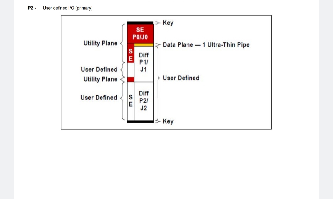
Signal Descriptions J5
| Signal Name | Description |
|---|---|
| ETH1-TPx | Ethernet port 1 signals (4 pair) 10/100/1000 twisted pair signals (Optional) |
| SER1-TXD | Asynchronous transmit serial data port 1 (out) / RS232 debug/console port only |
| SER1-RXD | Asynchronous received serial data port 1 (in) / RS232 debug/console port only |
| GND | System Ground (return) |
Rear I/O VPX Connectors P0-P2 (Conduction-Cooled)
The 68DT1 3U OpenVPX multifunction I/O board provides interface via the rear VPX connectors.
Rear I/O Summary
Signals defined as N/C currently have no functionality associated and are not required for general operation.
P0 - Utility plane. Contains the following signal definitions:
Power: Primary +5V, 3.3V_AUX, /- 12V and System GND
Geographical Address Pins: GA0# - GA4#, GAP#
Card reset: SYSRST# signal
VPX AUX/REF CLK (Not used)
P1 - Defined as primarily Data/Control Planes (User defined I/O secondary)
High Speed Switched Fabric Interface: One ultra-thin pipe option (PCIe ver. 2.0 (x1) or SRIO (1x)). Ethernet: Gig-E port option(s) are available and defined (See Part Number Designation section)
P2 - User defined I/O (primary)
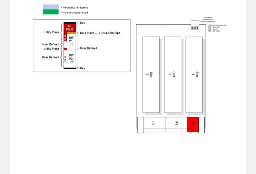
Rear I/O Utility Plane (P0)
The P0 (Utility) Plane contains the primary power, bus and utility signals for the OpenVPX board. Additionally, several of the user defined pins can be utilized for Geographical Addressing and a parallel SYSRST# signal. Signals defined as N/C currently have no functionality associated and is not required for general operation.
| UTILITY | Row | Row | Row | Row | Row | Row |
|---|---|---|---|---|---|---|
| Row | G | F | E | D | C | B |
| A | N/C (VS1_G1) | N/C (VS1_F1) | N/C (VS1_E1) | N/C (NCD1) | N/C (VS2_C1) | N/C VS2_B1) |
| N/C (VS2_A1) | N/C (VS1_G2) | N/C (VS1_F2) | N/C (VS1_E2) | N/C (NCD2) | N/C (VS2_C2) | N/C (VS2_B2) |
| N/C (VS2_A2) | (`)5V (VS3) | (`)5V (VS3) | (`)5V (VS3) | N/C (NCD3) | (`)5V (VS3) | (+)5V (VS3) |
| (+)5V (VS3) | IMPB-SCL-B (N/C) | IMPB-SDA-B (N/C) | GND | (-)12V (-12V_AUX) | GND | SYSRST# |
| N/C (NVMRO) | GAP# | GA4# | GND | (+)3.3V (+3.3V_AUX) | GND | IMPB-SCL-A (N/C) |
| IMPB-SDA-A (N/C) | GA3# | GA2# | GND | (+)12V (+12V_AUX) | GND | GA1# |
| GA0# | N/C (TCK) | GND | N/C (TDO) | N/C (TDI) | GND | N/C (TMS) |
| N/C (TRST) | GND | N/C*1 (REFCLK-25MHz-) | N/C*1 (REFCLK-25MHz+) | GND | N/C*1 (AUX-CLK-) | N/C*1 (AUX-CLK+) |
| GND |
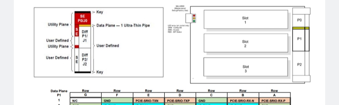
Rear I/O Data/Control Planes (P1)
The 68DT1 has the configuration option for specifying a high-speed serial interface fabric bus connections – PCIe ver. 2.0 (x1). As defined in the OpenVPX bridge or payload slot specifications, the 68DT1 requires only one ‘ultra-thin pipe’ (one Tx and one Rx differential pair), which provides additional user I/O definition opportunity. Additionally, the 68DT1 can be commanded/controlled via a front panel Gig-E interface (10/100/1000BaseT). Additional I/O is also defined on the P1 user defined plane. Signals defined as N/C currently have no functionality associated or are considered optional and are not required for general operation.
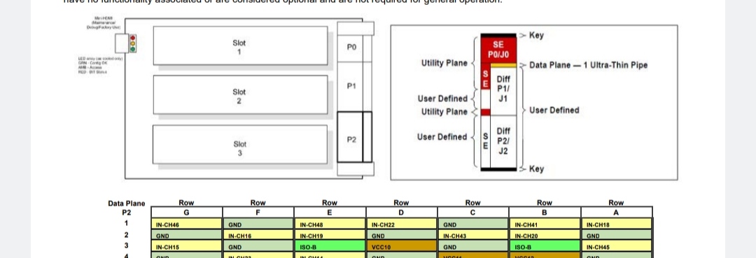
| Data Plane | Row | Row | Row | Row | Row | Row |
|---|---|---|---|---|---|---|
| Row | G | F | E | D | C | B |
| A | N/C | GND | PCIE-SRIO-TXN | PCIE-SRIO-TXP | GND | PCIE-SRIO-RX-N |
| PCIE-SRIO-RX-P | GND | IO-CH43 | IO-CH44 | GND | IO-CH48 | IO-CH47 |
| GND | N/C (VBAT) | GND | IO-CH46 | IO-CH45 | GND | IO-CH38 |
| IO-CH37 | GND | IO-CH39 | IO-CH32 | GND | IO-CH42 | IO-CH41 |
| GND | N/C | GND | ISO-C | VCC16 | GND | IO-CH26 |
| IO-CH31 | GND | IO-CH35 | IO-CH40 | GND | ISO-C | VCC15 |
| GND | N/C | GND | IO-CH34 | IO-CH33 | GND | IO-CH36 |
| IO-CH25 | GND | ISO-C | VCC13 | GND | IO-CH30 | IO-CH29 |
| GND | (SER-RXD1) | GND | IO-CH28 | IO-CH27 | GND | ISO-C |
| VCC14 | GND | ISO-B | IN-CH34 | GND | IN-CH28 | IN-CH25 |
| GND | (SER-TXD1 | GND | IN-CH29 | IN-CH26 | GND | IN-CH30 |
| IN-CH27 | GND | IN-CH40 | IN-CH31 | GND | IN-CH35 | IN-CH42 |
| GND | (SER-GND) | GND | IN-CH32 | IN-CH36 | GND | IN-CH44 |
| IN-CH33 | GND | IN-CH37 | IN-CH38 | GND | IN-CH39 | IN-CH24 |
| GND | N/C | GND | ETH-TP3N | ETH-TP3P | GND | ETH-TP2N |
| ETH-TP2P | GND | ETH-TP1N | ETH-TP1P | GND | ETH-TP0N | ETH-TP0P |
| GND |
USER I/O - Defined Area (User Defined I/O) (P2)
The following pages contain the ‘user defined’ I/O data area front and rear panel pin-outs with their respective signal designations for all module types currently offered/configured for the 68DT1 platform. The card is designed to route the function module I/O signals to the front and rear I/O connector. The following I/O connector pin-out is based upon the function module designated in the module slot. Signals defined as N/C currently have no functionality associated or are considered optional and are not required for general operation.
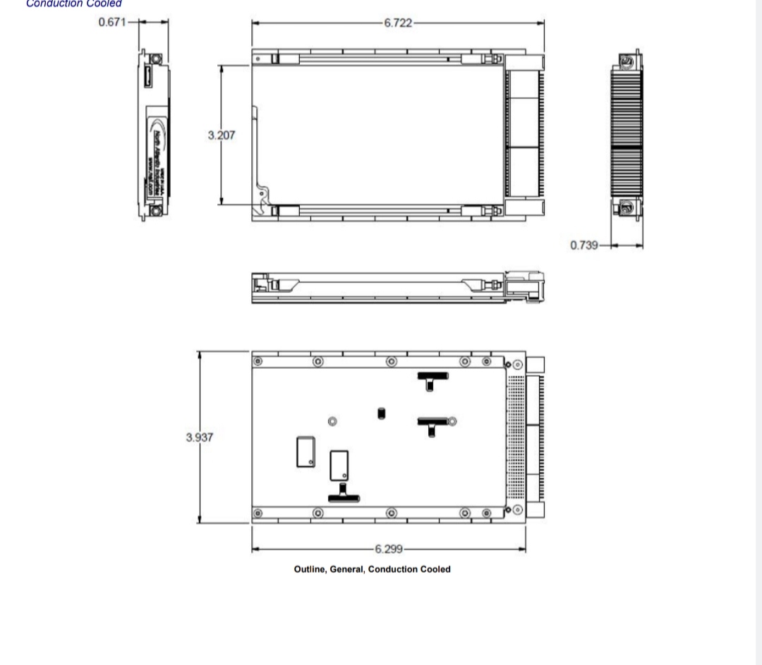
| Data Plane | Row | Row | Row | Row | Row | Row |
|---|---|---|---|---|---|---|
| Row | G | F | E | D | C | B |
| A | IN-CH46 | GND | IN-CH48 | IN-CH22 | GND | IN-CH41 |
| IN-CH18 | GND | IN-CH16 | IN-CH19 | GND | IN-CH43 | IN-CH20 |
| GND | IN-CH15 | GND | ISO-B | VCC10 | GND | ISO-B |
| IN-CH45 | GND | IN-CH23 | IN-CH14 | GND | VCC11 | VCC12 |
| GND | IN-CH10 | GND | IN-CH12 | IN-CH13 | GND | IN-CH17 |
| IN-CH08 | GND | VCC08 | VCC09 | GND | IN-CH11 | IN-CH09 |
| GND | IN-CH03 | GND | IN-CH06 | IN-CH07 | GND | VCC07 |
| ISO-B | GND | IO-CH14 | IN-CH04 | GND | IN-CH01 | IN-CH05 |
| GND | IN-CH21 | GND | IO-CH23 | IO-CH10 | GND | IN-CH02 |
| IO-CH18 | GND | IO-CH16 | IO-CH24 | GND | IO-CH21 | IO-CH22 |
| GND | IN-CH47 | GND | VCC05 | VCC06 | GND | IO-CH19 |
| IO-CH20 | GND | IO-CH12 | IO-CH17 | GND | ISO-A | VCC03 |
| GND | VCC02 | GND | IO-CH06 | IO-CH13 | GND | IO-CH15 |
| IO-CH11 | GND | ISO-A | VCC04 | GND | IO-CH09 | IO-CH08 |
| GND | VCC01 | GND | IO-CH07 | IO-CH05 | GND | ISO-A |
| ISO-A | GND | IO-CH04 | IO-CH03 | GND | IO-CH02 | IO-CH01 |
| GND |
MECHANICAL DETAILS
General - Outline
Note: The following mechanical outline detail examples are provided for reference only. Dimensions are in inches unless otherwise specified.
Conduction Cooled
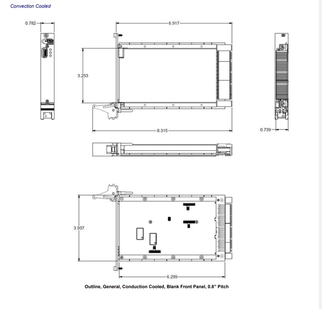
Convection Cooled
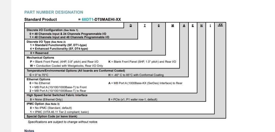
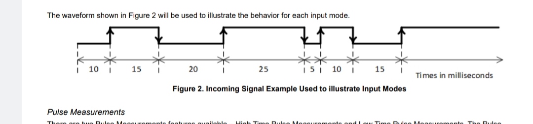
Notes
| 1. | Discrete I/O Configuration Define and factory configure the I/O channel availability. Discrete Input and/or Output specifications are defined per the DT1 (or DT4) -type function module. |
|---|---|
| 2. | Discrete I/O Type Discrete Input and/or Output functions are defined per the (SF) DT1-type or (EF) DT4-type function module specifications. Module (type) Channels Input Range Output Range Programmable Current Out (max./Ch.) Comments DT1/DT4* As configured 0-60 VDC 3-60 VDC (VCC) Input or Output/PWM ±500 mA Source/sink (out) (*) DT4 Enhanced Functionality (EF) Enhanced Mode Operations: Input: Pulse Measurements, Transition Timestamps, Transition Counters, Period Measurement and Frequency Measurement Output: PWM Output and Pattern Generator Output |
| 3. | IPMC Definition 0. OPTION “0”: DEFAULT. The board will not provide IPMC functionality. The board in this default configuration will boot normallywithout a Chassis Manager being present. 1. OPTION “1”: The board will provide VITA 46.11 Tier 2 compliant basic IPMC functionality. Note: When the IPMC option selected, the board will be configured expecting Chassis Manager communication on boot-up and requires the +3.3V-AUX power supply (PS) to be available on the backplane (provision of +3.3V-AUX is a VPX requirement). If no chassis manager communicates with this board with the IPMC option configured, the board will remain “off” until timeout (~ 10 seconds) and then will power-up/boot (PCIe enumeration cannot occur with board powered off). |
APPENDIX A: 68DT1 OPTIONAL ENHANCED INPUT/OUTPUT FUNCTIONALITY
Principle of Operation
The 68DT1 provides optional enhanced input and output mode functionality. For incoming signals (inputs), the enhanced modes include Pulse, Frequency and Period measurements. For outputs, the enhanced modes include PWM (Pulse Width Modulation) and Pattern Generation.
Input Modes
All input modes may be configured with debounce capability. Debounce capability allows configurable filtering of noisy signals and transients. Each channel may be set to an individual debounce time value. When a debounce time is set to a non-zero value, the signal reading after a transition must remain at the same level for the debounce interval before it is propagated through, otherwise it is rejected.
The waveform shown in Figure 2 will be used to illustrate the behavior for each input mode.
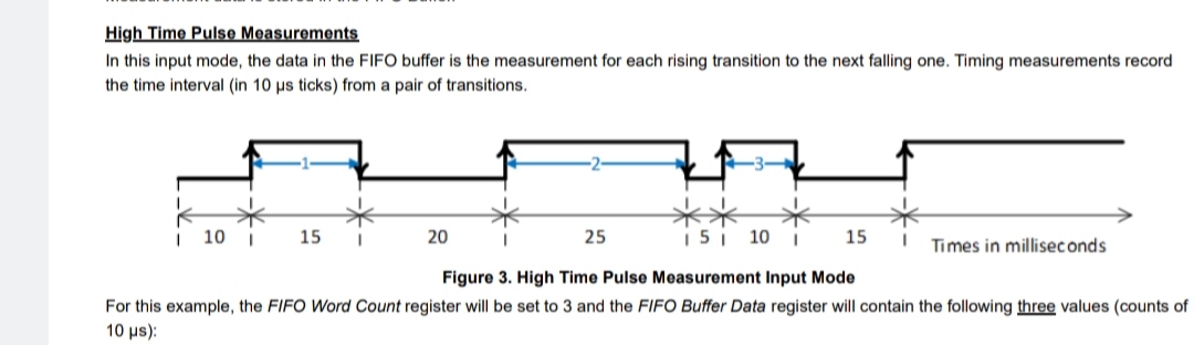
Pulse Measurements
There are two Pulse Measurements features available – High Time Pulse Measurements and Low Time Pulse Measurements. The Pulse Measurement data is stored in the FIFO Buffer.
High Time Pulse Measurements
In this input mode, the data in the FIFO buffer is the measurement for each rising transition to the next falling one. Timing measurements record the time interval (in 10 µs ticks) from a pair of transitions.
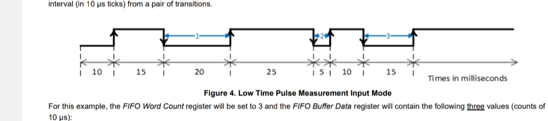
For this example, the FIFO Word Count register will be set to 3 and the FIFO Buffer Data register will contain the following three values (counts of 10 µs):
-
1500 (0x0000 05DC)
-
2500 (0x0000 09C4)
-
1000 (0x0000 03E8)
| Time Interval | Calculations | High Time Pulse Measurements |
|---|---|---|
| 1 | 1500 counts * 10 µsec = 15000 µsec = 15.0 msec | 15.0 msec |
| 2 | 2500 counts * 10 µsec = 25000 µsec = 25.0 msec | 25.0 msec |
| 3 | 1000 counts * 10 µsec = 10000 µsec = 10.0 msec | 10.0 msec |
Low Time Pulse Measurements
In this mode, the data in the FIFO buffer is the measurement for each falling edge to the next rising edge. Timing measurements record the time interval (in 10 µs ticks) from a pair of transitions.
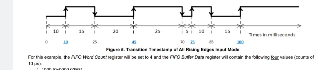
For this example, the FIFO Word Count register will be set to 3 and the FIFO Buffer Data register will contain the following three values (counts of 10 µs):
-
2000 (0x0000 07D0)
-
500 (0x0000 01F4)
-
1500 (0x0000 05DC)
| Time Interval | Calculations | Low Time Pulse Measurements |
|---|---|---|
| 1 | 2000 counts * 10 µsec = 20000 µsec = 20.0 msec | 20.0 msec |
| 2 | 500 counts * 10 µsec = 5000 µsec = 5.0 msec | 5.0 msec |
| 3 | 1500 counts * 10 µsec = 15000 µsec = 15.0 msec | 15.0 msec |
Transition Timestamps
There are three Transition Timestamp Measurements features available – Transition Timestamp for All Rising Edges, Transition Timestamp for All Falling Edges, and Transition Timestamp for All Edges. The Transition Timestamps Measurement data are store in the FIFO Buffer.
Transition Timestamp of All Rising Edges
In this mode, the data in the FIFO buffer is the Rising Edge Timestamp. The timestamp is a 32-bit counter that is incremented at the rate of 100 kHz (in other words, counter is incremented every 10 µsec). The timestamp is can be reset by the application at any time.
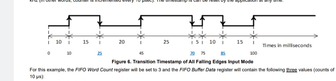
For this example, the FIFO Word Count register will be set to 4 and the FIFO Buffer Data register will contain the following four values (counts of 10 µs):
-
1000 (0x0000 03E8)
-
4500 (0x0000 1194)
-
7500 (0x0000 1D4C)
-
10000 (0x000 2710)
| Time Interval | Calculations | Time between rising edges |
|---|---|---|
| 1 to 2 | 4500 – 1000 = 3500 counts = 3500 * 10 µsec = 35000 µsec = 35.0 msec | 35.0 msec |
| 2 to 3 | 7500 – 4500 = 3000 counts = 3000 * 10 µsec = 30000 µsec = 30.0 msec | 30.0 msec |
| 3 to 4 | 10000 – 7500 = 2500 counts = 2500 * 10 µsec = 25000 µsec = 25.0 msec | 25.0 msec |
Transition Timestamp of All Falling Edges
In this mode, the data in the FIFO buffer is the Falling Edge Timestamp. The timestamp is a 32-bit counter that is incremented at the rate of 100 kHz (in other words, counter is incremented every 10 µsec). The timestamp is can be reset by the application at any time.
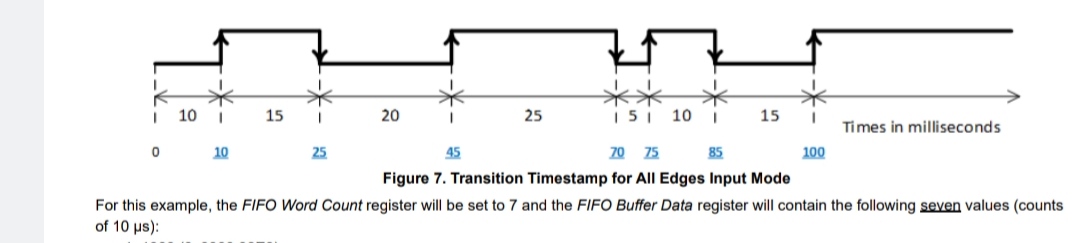
For this example, the FIFO Word Count register will be set to 3 and the FIFO Buffer Data register will contain the following three values (counts of 10 µs):
-
2500 (0x0000 09C4)
-
7000 (0x0000 1B58)
-
8500 (0x0000 2134)
| Time Interval | Calculations | Time between falling edges |
|---|---|---|
| 1 to 2 | 7000 – 2500 = 4500 counts = 4500 * 10 µsec = 45000 µsec = 45.0 msec | 45.0 msec |
| 2 to 3 | 8500 – 7000 = 1500 counts = 1500 * 10 µsec = 15000 µsec = 15.0 msec | 15.0 msec |
Transition Timestamp of All Edges
In this mode, the data in the FIFO buffer is the Rising and Falling Edge Timestamp. The timestamp is a 32-bit counter that is incremented at the rate of 100 kHz (in other words, counter is incremented every 10 µsec). The timestamp is can be reset by the application at any time.
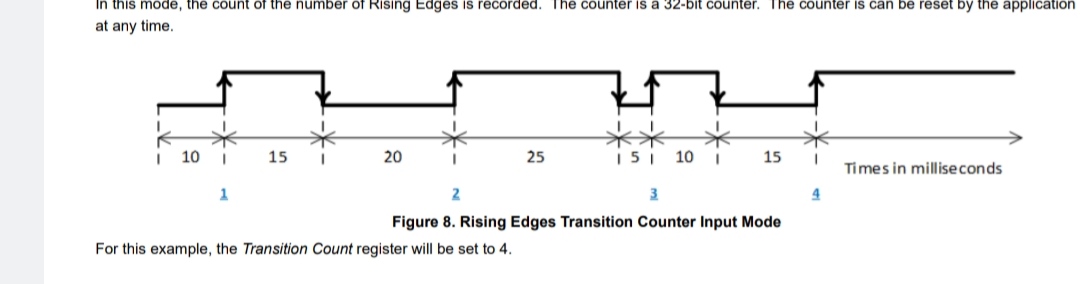
For this example, the FIFO Word Count register will be set to 7 and the FIFO Buffer Data register will contain the following seven values (counts of 10 µs):
-
1000 (0x0000 03E8)
-
2500 (0x0000 09C4)
-
4500 (0x0000 1194)
-
7000 (0x0000 1B58)
-
7500 (0x0000 1D4C)
-
8500 (0x0000 2134)
-
10000 (0x000 2710)
| Time Interval | Calculations | Time between edges |
|---|---|---|
| 1 to 2 | 2500 – 1000 = 1500 counts = 1500 * 10 µsec = 15000 µsec = 15.0 msec | 15.0 msec |
| 2 to 3 | 4500 – 2500 = 2000 counts = 2000 * 10 µsec = 20000 µsec = 20.0 msec | 20.0 msec |
| 3 to 4 | 7000 – 4500 = 2500 counts = 2500 * 10 µsec = 25000 µsec = 25.0 msec | 25.0 msec |
| 4 to 5 | 7500 – 7000 = 500 counts = 500 * 10 µsec = 5000 µsec = 5.0 msec | 5.0 msec |
| 5 to 6 | 8500 – 7500 = 1000 counts = 1000 * 10 µsec = 10000 µsec = 10.0 msec | 10.0 msec |
| 6 to 7 | 10000 – 8500 = 1500 counts = 1500 * 10 µsec = 15000 µsec = 15.0 msec | 15.0 msec |
Transition Counter
There are three Transition Counter features available – Rising Edge Transition Counter, Falling Edge Transition Counter and All Edge Transition Counter.
Rising Edges Transition Counter
In this mode, the count of the number of Rising Edges is recorded. The counter is a 32-bit counter. The counter is can be reset by the application at any time.
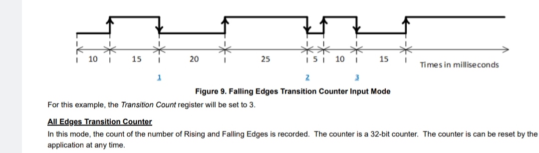
For this example, the Transition Count register will be set to 4.
Falling Edges Transition Counter
In this mode, the count of the number of Falling Edges is recorded. The counter is a 32-bit counter. The counter is can be reset by the application at any time.
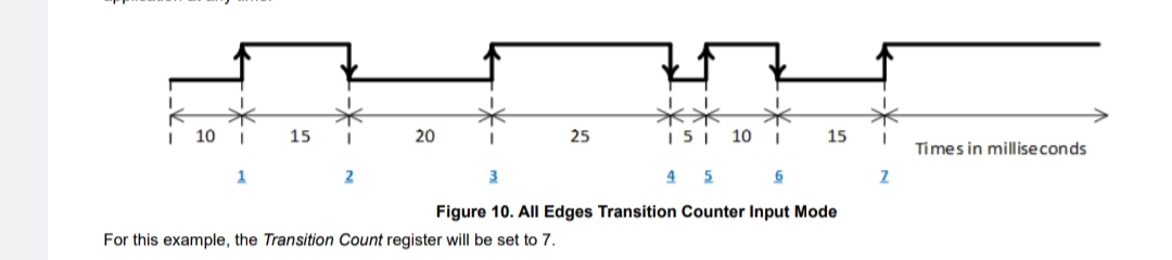
For this example, the Transition Count register will be set to 3.
All Edges Transition Counter
In this mode, the count of the number of Rising and Falling Edges is recorded. The counter is a 32-bit counter. The counter is can be reset by the application at any time.
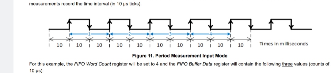
For this example, the Transition Count register will be set to 7.
Period Measurement
In this input mode, the data in the FIFO buffer is the measurement for each rising edge transition to the next rising edge transition. Timing measurements record the time interval (in 10 µs ticks).
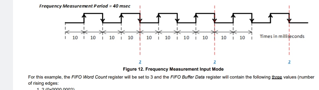
For this example, the FIFO Word Count register will be set to 4 and the FIFO Buffer Data register will contain the following three values (counts of 10 µs):
-
2000 (0x0000 07D0) 2. 2000 (0x0000 07D0)
-
2000 (0x0000 07D0)
-
2000 (0x0000 07D0)
| Time Interval | Calculations | Period Measurements |
|---|---|---|
| 1 | 2000 counts * 10 µsec = 20000 µsec = 20.0 msec | 20.0 msec |
| 2 | 2000 counts * 10 µsec = 20000 µsec = 20.0 msec | 20.0 msec |
| 3 | 2000 counts * 10 µsec = 20000 µsec = 20.0 msec | 20.0 msec |
| 4 | 2000 counts * 10 µsec = 20000 µsec = 20.0 msec | 20.0 msec |
Frequency Measurement
In this input mode, the data in the FIFO buffer is the number of rising edge transitions for the programmable time interval programmed in the Frequency Measurement Period register.
For this example, set the Frequency Measurement Period register = 4000 (4000 * 10 µs = 40000 µs = 40 msec).
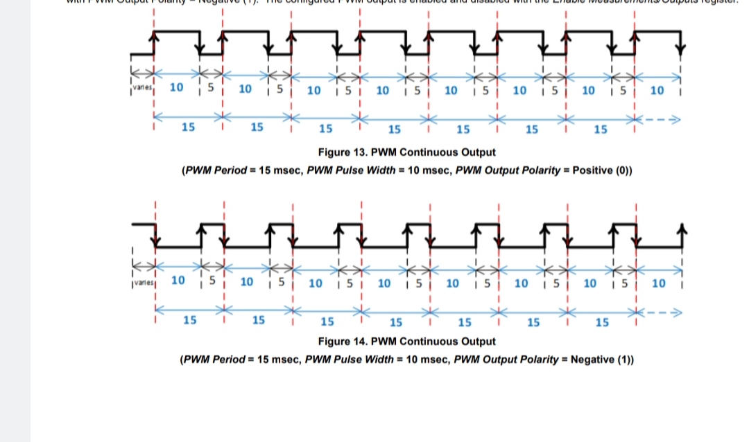
For this example, the FIFO Word Count register will be set to 3 and the FIFO Buffer Data register will contain the following three values (number of rising edges:
- 2 (0x0000 0002) 2. 2 (0x0000 0002) 3. 2 (0x0000 0002)
| Time Interval | Calculations | Frequency Measurements |
|---|---|---|
| 1 | 2 counts/40 msec = 2 counts/0.04 seconds = 50 Hz | 50 Hz |
| 2 | 2 counts/40 msec = 2 counts/0.04 seconds = 50 Hz | 50 Hz |
| 3 | 2 counts/40 msec = 2 counts/0.04 seconds = 50 Hz | 50 Hz |
Output Modes
There are three Enhanced Output Functionality modes: two PWM outputs and one Pattern Generator Output mode.
PWM Output
There are two PWM output modes, PWM Continuous and PWM Burst. The PWM timing is very precise with low jitter. In PWM Output mode, the Mode Select register is set to either “PWM Continuous or PWM Burst”. The value written to the PWM Period register specifies the period to output the PWM signal, the value written to the PWM Pulse Width register specifies the time for the “ON” state, and the value written to the PWM Output Polarity register specifies the initial edge of the output. For PWM Burst mode, the PWM Number of Cycles register specifies the number of cycles to output the signal. Note, there may be an initial “OFF” state level delay based on the Period time before the initial pulse is output.
PWM Continuous
Figure 12 and Figure 13 illustrate the PWM Continuous Output signal, one configured with PWM Output Polarity = Positive (0) and one configured with PWM Output Polarity = Negative (1). The configured PWM output is enabled and disabled with the Enable Measurements/Outputs register.
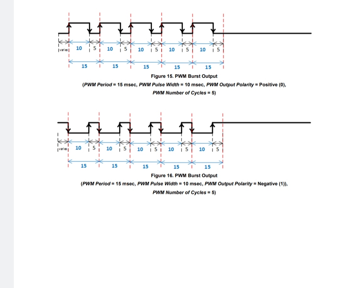
PWM Burst
Figure 14 and Figure 15 illustrate the PWM Burst Output signal with the PWM Number of Cycles = 5 pulses, one configured with PWM Output Polarity = Positive (0) and one configured with PWM Output Polarity = Negative (1). The configured PWM output is enabled with the Enable Measurements/Outputs register. Once the number of pulses that were requested is outputted, the value in the Enable Measurements/Outputs register will be reset (self-clearing) to allow for the output to be re-enabled.
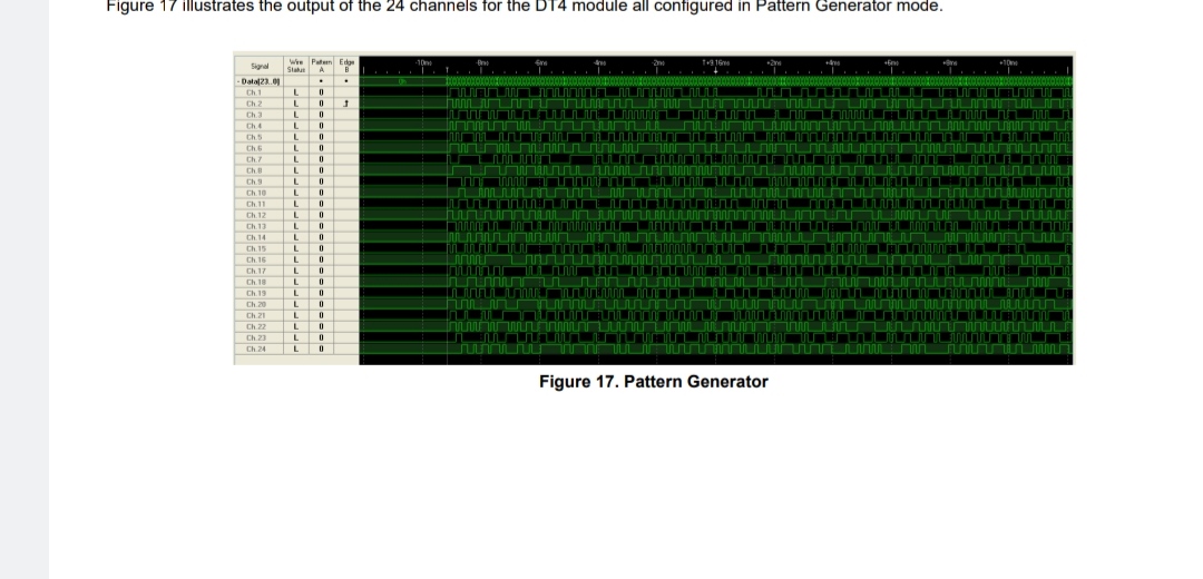
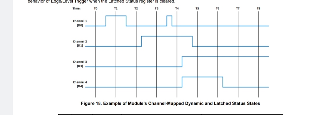
Pattern Generator
For the Pattern Generator mode, there is 64K block of unsigned 32-bit words allocated to specify the data pattern for the output channels. The data in each 32-bit word is bit-mapped per channel. The Pattern RAM Start Address and Pattern RAM End Address registers specify the starting and ending address in the 64K block to use as the data to output for each channel configured for Pattern Generator mode. The Pattern RAM Period register specifies the pattern rate. The Pattern RAM Control and Pattern RAM Number of Cycles control the Pattern Generator output – Continuous, Burst with a specified number of cycles, Pause, or External Trigger from input from Channel 1. Note, when any channel is configured for External Trigger Pattern Generator mode, Channel 1 must be set as an input.
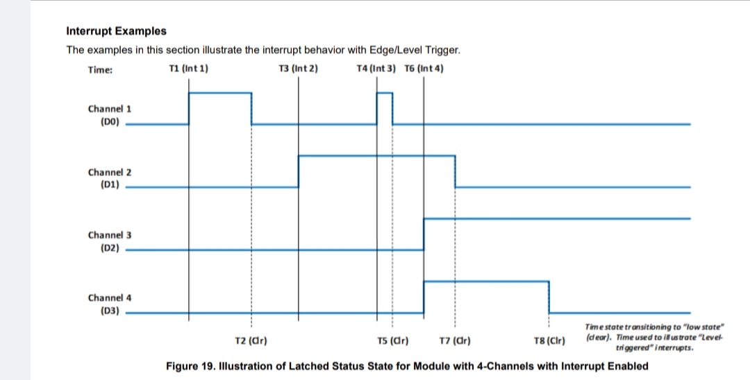
Register Descriptions
The register descriptions provide the register name, Type, Data Range, Read or Write information, Initialized Value, and a description of the function.
Enhanced I/O Functionality Registers
The modules listed in section 1 provide enhanced input and output mode functionality. The Mode Select and Enable Output/Measurement registers are general control registers for the different enhanced input and output modes.
Mode Select
Function: Configures the Enhanced Functionality Modes to apply to the channel.
Type: unsigned binary word (32-bit)
Data Range: See table
Read/Write: R/W
Initialized Value: 0
Operational Settings: It is important that the channel is correctly configured to either input or output in the Input/Output Format registers to correspond to the Enhanced Functionality Mode selected. Setting a 0 to this register will configure that channel to normal operation.
| Mode Select Value (Decimal) | Mode Select Value (Hexadecimal) | Description |
|---|---|---|
| 0 | 0x0000 0000 | Enhanced Functionality Disabled |
| Input Enhanced Functionality Mode | 1 | 0x0000 0001 |
| High Time Pulse Measurements | 2 | 0x0000 0002 |
| Low Time Pulse Measurements | 3 | 0x0000 0003 |
| Transition Timestamp of All Rising Edges | 4 | 0x0000 0004 |
| Transition Timestamp of All Falling Edges | 5 | 0x0000 0005 |
| Transition Timestamp of All Edges | 6 | 0x0000 0006 |
| Rising Edges Transition Counter | 7 | 0x0000 0007 |
| Falling Edges Transition Counter | 8 | 0x0000 0008 |
| All Edges Transition Counter | 9 | 0x0000 0009 |
| Period Measurement | 10 | 0x0000 000A |
| Frequency Measurement Output Enhanced Functionality Mode | 32 | 0x0000 0020 |
| PWM Continuous | 33 | 0x0000 0021 |
| PWM Burst | 34 | 0x0000 0022 |
| Pattern Generator |
Enable Measurements/Outputs
Function: Enables/starts the measurements or outputs based on the Mode Select for the channel. Type: unsigned binary word (32-bit)
Data Range: 0x0000 0000 to 0x00FF FFFF
Read/Write: R/W
Initialized Value: 0
Operational Settings: Setting the bit for the associated channel to a “1” will start the measurement or output depending on the Mode Select configuration for that channel. Setting the bit for the associated channel to “0” will stop the measurements/outputs.
Enable Measurements/Outputs
| D31 | D30 | D29 | D28 | D27 | D26 | D25 | D24 | D23 | D22 | D21 | D20 | D19 | D18 | D17 | D16 |
|---|---|---|---|---|---|---|---|---|---|---|---|---|---|---|---|
| 0 | 0 | 0 | 0 | 0 | 0 | 0 | 0 | Ch24 | Ch23 | Ch22 | Ch21 | Ch20 | Ch19 | Ch18 | Ch17 |
| D15 | D14 | D13 | D12 | D11 | D10 | D9 | D8 | D7 | D6 | D5 | D4 | D3 | D2 | D1 | D0 |
| Ch16 | Ch15 | Ch14 | Ch13 | Ch12 | Ch11 | Ch10 | Ch9 | Ch8 | Ch7 | Ch6 | Ch5 | Ch4 | Ch3 | Ch2 | Ch1 |
Input Modes Registers
After configuring the Mode Select register, write a “1” to the Reset Timer/Counter register resets the channel’s timestamp and counter used for input modes. Write a “1” to the Enable Measurements/Outputs register to begin the measurement of the input signal. Write a “0” to the Enable Measurements/Outputs register to stop the measurement of the input signal. The data can be read either while the measurements are being made on input signals or after stopping the measurements.
Reset Timer/Counter
Function: Resets the measurement timestamp and counter for the channel.
Type: unsigned binary word (32-bit)
Data Range: 0x0000 0000 to 0x00FF FFFF
Read/Write: W
Initialized Value: 0
Operational Settings: Setting the bit for the associated channel to a “1” will:
• reset the timestamp used for the Pulse Measurements mode (1-2), Transition Timestamp mode (3-5), and Period Measurement mode (9) and Frequency Measurement mode (10) • reset the counter used for Transition Counter mode (6-8)
Reset Timer/Counter
| D31 | D30 | D29 | D28 | D27 | D26 | D25 | D24 | D23 | D22 | D21 | D20 | D19 | D18 | D17 | D16 |
|---|---|---|---|---|---|---|---|---|---|---|---|---|---|---|---|
| 0 | 0 | 0 | 0 | 0 | 0 | 0 | 0 | Ch24 | Ch23 | Ch22 | Ch21 | Ch20 | Ch19 | Ch18 | Ch17 |
| D15 | D14 | D13 | D12 | D11 | D10 | D9 | D8 | D7 | D6 | D5 | D4 | D3 | D2 | D1 | D0 |
| Ch16 | Ch15 | Ch14 | Ch13 | Ch12 | Ch11 | Ch10 | Ch9 | Ch8 | Ch7 | Ch6 | Ch5 | Ch4 | Ch3 | Ch2 | Ch1 |
FIFO Registers
The FIFO registers are used for the following input modes:
• Pulse Measurements mode (1-2)
• Transition Timestamp mode (3-5)
• Period Measurement mode (9)
• Frequency Measurement mode (10)
FIFO Buffer Data
Function: The data stored in the FIFO Buffer Data is dependent on the input mode.
Type: unsigned binary word (32-bit)
Data Range: 0x0000 0000 to 0xFFFF FFFF
Read/Write: R
Initialized Value: N/A
Operational Settings: Refer to examples in section 2.1.
FIFO Word Count
Function: This is a counter that reports the number of 32-bit words stored in the FIFO buffer.
Type: unsigned binary word (32-bit)
Data Range: 0 – 255 (0x0000 0000 to 0x0000 00FF)
Read/Write: R
Initialized Value: 0
Operational Settings: Every time a read operation is made from the FIFO Buffer Data register, the value in the FIFO Word Count register will be decremented by one. The maximum number of words that can be stored in the FIFO is 255.
FIFO Word Count
| D31 | D30 | D29 | D28 | D27 | D26 | D25 | D24 | D23 | D22 | D21 | D20 | D19 | D18 | D17 | D16 |
|---|---|---|---|---|---|---|---|---|---|---|---|---|---|---|---|
| 0 | 0 | 0 | 0 | 0 | 0 | 0 | 0 | 0 | 0 | 0 | 0 | 0 | 0 | 0 | 0 |
| D15 | D14 | D13 | D12 | D11 | D10 | D9 | D8 | D7 | D6 | D5 | D4 | D3 | D2 | D1 | D0 |
| 0 | 0 | 0 | 0 | 0 | 0 | 0 | 0 | D | D | D | D | D | D | D | D |
Clear FIFO
Function: Clears FIFO by resetting the FIFO Word Count register.
Type: unsigned binary word (32-bit)
Data Range: 0 or 1
Read/Write: W
Initialized Value: N/A
Operational Settings: Write a 1 to resets the Words in FIFO to zero; Clear FIFO register does not clear data in the buffer. A read to the buffer data will give “aged” data.
| D31-D1 | Reserved. Set to 0 |
|---|---|
| D0 | Set to 1 to reset the FIFO Word Count value to zero. |
Clear FIFO
| D31 | D30 | D29 | D28 | D27 | D26 | D25 | D24 | D23 | D22 | D21 | D20 | D19 | D18 | D17 | D16 |
|---|---|---|---|---|---|---|---|---|---|---|---|---|---|---|---|
| 0 | 0 | 0 | 0 | 0 | 0 | 0 | 0 | 0 | 0 | 0 | 0 | 0 | 0 | 0 | 0 |
| D15 | D14 | D13 | D12 | D11 | D10 | D9 | D8 | D7 | D6 | D5 | D4 | D3 | D2 | D1 | D0 |
| 0 | 0 | 0 | 0 | 0 | 0 | 0 | 0 | 0 | 0 | 0 | 0 | 0 | 0 | 0 | D |
FIFO Status
Function: Sets the corresponding bit associated with the FIFO status type; there is a separate register for each channel.
Type: unsigned binary word (32-bit)
Data Range: See table
Read/Write: R
Initialized Value: 0
Description
| D31-D4 | Reserved | Set to 0 |
|---|---|---|
| D3 | Empty | Set to 1 when FIFO Word Count = 0 |
| D2 | Almost Empty | Set to 1 when FIFO Word Count ⇐ 63 (25%) |
| D1 | Almost Full | Set to 1 when FIFO Word Count >= 191 (75%) |
| D0 | Full | Set to 1 when FIFO Word Count = 255 |
FIFO Status
| D31 | D30 | D29 | D28 | D27 | D26 | D25 | D24 | D23 | D22 | D21 | D20 | D19 | D18 | D17 | D16 |
|---|---|---|---|---|---|---|---|---|---|---|---|---|---|---|---|
| 0 | 0 | 0 | 0 | 0 | 0 | 0 | 0 | 0 | 0 | 0 | 0 | 0 | 0 | 0 | 0 |
| D15 | D14 | D13 | D12 | D11 | D10 | D9 | D8 | D7 | D6 | D5 | D4 | D3 | D2 | D1 | D0 |
| 0 | 0 | 0 | 0 | 0 | 0 | 0 | 0 | 0 | 0 | 0 | 0 | D | D | D | D |
Transition Count Registers
The Transition Count register are used for the following input modes: • Transition Counter mode (6-8)
Transition Count
Function: Contains the count of the transitions depending on the configuration in the Mode Select register – Rising Edges, Falling Edges or All Edges.
Type: unsigned binary word (32-bit)
Data Range: 0x0000 0000 to 0xFFFF FFFF
Read/Write: R
Initialized Value: 0
Operational Settings: Refer to examples in section 2.1.3.
Frequency Measurement Registers
For the Frequency Measurement mode, the period to perform the frequency measurements must be specified in the Frequency Measurement Period register.
Frequency Measurement Period
Function: When the Mode Select register is programmed for Frequency Measurement mode (10), the value in the Frequency Measurement Period is used as the time interval for counting the number of rising edge transitions within that interval.
Type: unsigned binary word (32-bit)
Data Range: 0x0 to 0xFFFF FFFF
Read/Write: R/W
Initialized Value: 0
Operational Settings: Set the Frequency Measurement Period (LSB = 10 µs). Refer to examples in section 2.1.5.
Output Modes Registers
After configuring the Mode Select register, write a “1” to the Enable Measurements/Outputs register to outputting the signal. Write a “0” to the Enable Measurements/Outputs register to stop the output signal.
PWM Registers
The PWM Period, PWM Pulse Width and PWM Output Polarity registers configure the PWM output signal. When the Mode Select register is configured for PWM Burst mode, the PWM Number of Cycles register is used to specify the number of cycles to repeat for the burst.
PWM Period
Function: When the Mode Select register is programmed for PWM Continuous or PWM Burst mode (32-33), the value in the PWM Period is used as the time interval for outputting the PWM signal.
Type: unsigned binary word (32-bit)
Data Range: 0x0000 0001 to 0xFFFF FFFF
Read/Write: R/W
Initialized Value: 0
Operational Settings: Set the PWM Period (LSB = 10 µs). The PWM Period must be greater than the value set in the PWM Pulse Width register. Refer to examples in section 2.2.1.
PWM Pulse Width
Function: When the Mode Select register is programmed for PWM Continuous or PWM Burst mode (32-33), the value in the PWM Pulse Width is used as the time interval of the “ON” state for outputting the PWM signal.
Type: unsigned binary word (32-bit)
Data Range: 0x0 to 0xFFFF FFFF
Read/Write: R/W
Initialized Value: 0
Operational Settings: Set the PWM Pulse Width (LSB = 10 µs). The PWM Pulse Width must be less than the value set in the PWM Pulse Width register. Refer to examples in section 2.2.1.
PWM Output Polarity
Function: When the Mode Select register is programmed for PWM Continuous or PWM Burst mode (32-33), the value in the PWM Output Polarity is used to specify whether the PWM output signal starts with a rising edge (Positive (0)), or a falling edge (Negative (1)).
Type: unsigned binary word (32-bit)
Data Range: 0x0 to 0x00FF FFFF
Read/Write: R/W
Initialized Value: 0
Operational Settings: The PWM Output Polarity register is used to program the starting edge of the PWM Pulse Period (rising or falling). When the PWM output Polarity is set to Positive (0), the output will start with a rising edge, when it’s set to Negative (1), the output will start with a falling edge. The default is Positive (0), which is set when the PWM Polarity bit is 0. Refer to examples in section 2.2.1.
PWM Output Polarity
| D31 | D30 | D29 | D28 | D27 | D26 | D25 | D24 | D23 | D22 | D21 | D20 | D19 | D18 | D17 | D16 |
|---|---|---|---|---|---|---|---|---|---|---|---|---|---|---|---|
| 0 | 0 | 0 | 0 | 0 | 0 | 0 | 0 | Ch24 | Ch23 | Ch22 | Ch21 | Ch20 | Ch19 | Ch18 | Ch17 |
| D15 | D14 | D13 | D12 | D11 | D10 | D9 | D8 | D7 | D6 | D5 | D4 | D3 | D2 | D1 | D0 |
| Ch16 | Ch15 | Ch14 | Ch13 | Ch12 | Ch11 | Ch10 | Ch9 | Ch8 | Ch7 | Ch6 | Ch5 | Ch4 | Ch3 | Ch2 | Ch1 |
PWM Number of Cycles
Function: When the Mode Select register is programmed for PWM Burst mode (33), the value in the PWM Number of Cycles is used to specify the number of times to repeat the PWM output signal.
Type: unsigned binary word (32-bit)
Data Range: 0x0000 0001 to 0xFFFF FFFF
Read/Write: R/W
Initialized Value: 0
Operational Settings: Set the number of times to output the PWM signal. Refer to examples in section 2.2.1.
Pattern Generator Registers
The Pattern RAM registers are a 64K block of unsigned 32-bit words allocated to specify the data pattern for the output channels. The Pattern RAM Start Address, Pattern RAM End Address, Pattern RAM Period and Pattern RAM Control registers configure the Pattern Generator output signals. When the Pattern RAM Control register is configured for Burst, the Pattern RAM Number of Cycles specify the number of cycles to repeat the pattern for the burst.
Pattern RAM
Function: Pattern Generator Memory Block from 0x40000 to 0x7FFFC.
Type: unsigned binary word (32-bit)
Address Range: 0x0000 0000 to 0x00FF FFFF
Read/Write: R/W
Initialized Value: 0
Operational Settings: 64K block of unsigned 32-bit words. The data in each 32-bit word is bit-mapped per channel.
Pattern RAM
| D31 | D30 | D29 | D28 | D27 | D26 | D25 | D24 | D23 | D22 | D21 | D20 | D19 | D18 | D17 | D16 |
|---|---|---|---|---|---|---|---|---|---|---|---|---|---|---|---|
| 0 | 0 | 0 | 0 | 0 | 0 | 0 | 0 | Ch24 | Ch23 | Ch22 | Ch21 | Ch20 | Ch19 | Ch18 | Ch17 |
| D15 | D14 | D13 | D12 | D11 | D10 | D9 | D8 | D7 | D6 | D5 | D4 | D3 | D2 | D1 | D0 |
| Ch16 | Ch15 | Ch14 | Ch13 | Ch12 | Ch11 | Ch10 | Ch9 | Ch8 | Ch7 | Ch6 | Ch5 | Ch4 | Ch3 | Ch2 | Ch1 |
Pattern RAM Start Address
Function: When the Mode Select register is programmed for Pattern Generator mode (34), the Pattern RAM Start Address register specifies the starting address within the Pattern RAM block registers to use for the output.
Type: unsigned binary word (32-bit)
Data Range: 0x0004 0000 to 0x0007 FFFC
Read/Write: R/W
Initialized Value: 0
Operational Settings: The value in the Pattern RAM Start Address must be less than the value in the Pattern RAM End Address.
Pattern RAM Start Address
| D31 | D30 | D29 | D28 | D27 | D26 | D25 | D24 | D23 | D22 | D21 | D20 | D19 | D18 | D17 | D16 |
|---|---|---|---|---|---|---|---|---|---|---|---|---|---|---|---|
| 0 | 0 | 0 | 0 | 0 | 0 | 0 | 0 | 0 | 0 | 0 | 0 | 0 | D | D | D |
| D15 | D14 | D13 | D12 | D11 | D10 | D9 | D8 | D7 | D6 | D5 | D4 | D3 | D2 | D1 | D0 |
| D | D | D | D | D | D | D | D | D | D | D | D | D | D | D | D |
Pattern RAM End Address
Function: When the Mode Select register is programmed for Pattern Generator mode (34), the Pattern RAM End Address register specifies the end address within the Pattern RAM block registers to use for the output.
Type: unsigned binary word (32-bit)
Data Range: 0x40000 to 0x7FFFC
Read/Write: R/W
Initialized Value: 0
Operational Settings: The value in the Pattern RAM End Address must be greater than the value in the Pattern RAM Start Address.
Pattern RAM End Address
| D31 | D30 | D29 | D28 | D27 | D26 | D25 | D24 | D23 | D22 | D21 | D20 | D19 | D18 | D17 | D16 |
|---|---|---|---|---|---|---|---|---|---|---|---|---|---|---|---|
| 0 | 0 | 0 | 0 | 0 | 0 | 0 | 0 | 0 | 0 | 0 | 0 | 0 | D | D | D |
| D15 | D14 | D13 | D12 | D11 | D10 | D9 | D8 | D7 | D6 | D5 | D4 | D3 | D2 | D1 | D0 |
| D | D | D | D | D | D | D | D | D | D | D | D | D | D | D | D |
Pattern RAM Period
Function: When the Mode Select register is programmed for Pattern Generator mode (34), the value in the Pattern RAM Period is used as the time interval for outputting the Pattern Generator signals.
Type: unsigned binary word (32-bit)
Data Range: 0x0000 0001 to 0xFFFF FFFF
Read/Write: R/W
Initialized Value: 0
Operational Settings: Set the Pattern RAM Period (LSB = 10 µs).
Pattern RAM Control
Function: When the Mode Select register is programmed for Pattern Generator mode (34), the value in the Pattern RAM Control is used to control the outputting of the Pattern Generator signals.
Type: unsigned binary word (32-bit)
Data Range: See table
Read/Write: R/W
Initialized Value: 0
Operational Settings: Configures the Patter Generator for Continuous, Burst with a specified number of cycles, Pause, or External Trigger from input from Channel 1. Note, when any channel is configured for External Trigger Pattern Generator mode, Channel 1 must be set as an input.
| Bits | Description |
|---|---|
| D31-D5 | Reserved. Set to 0 |
| D4 | Falling Edge External Trigger – Channel 1 used as the input for the trigger |
| D3 | Rising Edge External Trigger – Channel 1 used as the input for the trigger |
| D2 | Pause |
| D1 | Burst Mode – value in Pattern RAM Number of Cycles register defines number of cycles to output |
| D0 | Enable Pattern Generator |
| Values | Description |
|---|---|
| 0x0000 | Disable Pattern Generator, Continuous Mode, No External Trigger |
| 0x0001 | Enable Pattern Generator, Continuous Mode, No External Trigger |
| 0x0002 | Disable Pattern Generator, Burst Mode, No External Trigger |
| 0x0003 | Enable Pattern Generator, Burst Mode, No External Trigger |
| 0x0005 | Enable Pattern Generator, Continuous Mode, Pause, No External Trigger |
| 0x0007 | Enable Pattern Generator, Burst Mode, Pause, No External Trigger |
| 0x0008 | Disable Pattern Generator, Continuous Mode, Rising External Trigger |
| 0x0009 | Enable Pattern Generator, Continuous Mode, Rising External Trigger |
| 0x000A | Disable Pattern Generator, Burst Mode, Rising External Trigger |
| 0x000B | Enable Pattern Generator, Burst Mode, Rising External Trigger |
| 0x000D | Enable Pattern Generator, Continuous Mode, Pause, Rising External Trigger |
| 0x000F | Enable Pattern Generator, Burst Mode, Pause, Rising External Trigger |
| 0x1000 | Disable Pattern Generator, Continuous Mode, Falling External Trigger |
| 0x1001 | Enable Pattern Generator, Continuous Mode, Falling External Trigger |
| 0x1002 | Disable Pattern Generator, Burst Mode, Falling External Trigger |
| 0x1003 | Enable Pattern Generator, Burst Mode, Falling External Trigger |
| 0x1005 | Enable Pattern Generator, Continuous Mode, Pause, Falling External Trigger |
| 0x1007 | Enable Pattern Generator, Burst Mode, Pause, Falling External Trigger |
| 0x0004, 0x0006, 0x000C, 0x000E, 0x1004, 0x1006, 0x1008-0x100F | Invalid |
Pattern RAM Control
| D31 | D30 | D29 | D28 | D27 | D26 | D25 | D24 | D23 | D22 | D21 | D20 | D19 | D18 | D17 | D16 |
|---|---|---|---|---|---|---|---|---|---|---|---|---|---|---|---|
| 0 | 0 | 0 | 0 | 0 | 0 | 0 | 0 | 0 | 0 | 0 | 0 | 0 | 0 | 0 | 0 |
| D15 | D14 | D13 | D12 | D11 | D10 | D9 | D8 | D7 | D6 | D5 | D4 | D3 | D2 | D1 | D0 |
| 0 | 0 | 0 | 0 | 0 | 0 | 0 | 0 | 0 | 0 | 0 | 0 | D | D | D | D |
Pattern RAM Number of Cycles
Function: When the Mode Select register is programmed for Pattern Generator mode (34) and the Pattern RAM Control register is set for Burst mode, the value in the Pattern RAM Number of Cycles is used to specify the number of times to repeat the pattern output signal.
Type: unsigned binary word (32-bit)
Data Range: 0x0000 0001 to 0xFFFF FFFF
Read/Write: R/W
Initialized Value: 0
Operational Settings: Set the number of times to output the pattern.
Function Register Map
Key: Bold Italic = Configuration/Control Bold Underline = State/Measurement/Status
*When an event is detected, the bit associated with the event is set in this register and will remain set until the user clears the event bit. Clearing the bit requires writing a 1 back to the specific bit that was set when read (i.e., write-1-to-clear, writing a “1” to a bit set to “1” will set the bit to “0).
- Data is represented in Floating Point if Enable Floating Point Mode register is set to Floating Point Mode (1).
Enhanced Input (DT-IN Ch 1-24, 25-48) Functionality Registers
| 0x1028 | Mode Select DT-IN Ch 1 | R/W |
|---|---|---|
| 0x1068 | Mode Select DT-IN Ch 2 | R/W |
| 0x10A8 | Mode Select DT-IN Ch 3 | R/W |
| 0x10E8 | Mode Select DT-IN Ch 4 | R/W |
| 0x1128 | Mode Select DT-IN Ch 5 | R/W |
| 0x1168 | Mode Select DT-IN Ch 6 | R/W |
| 0x11A8 | Mode Select DT-IN Ch 7 | R/W |
| 0x11E8 | Mode Select DT-IN Ch 8 | R/W |
| 0x1228 | Mode Select DT-IN Ch 9 | R/W |
| 0x1268 | Mode Select DT-IN Ch 10 | R/W |
| 0x12A8 | Mode Select DT-IN Ch 11 | R/W |
| 0x12E8 | Mode Select DT-IN Ch 12 | R/W |
| 0x1328 | Mode Select DT-IN Ch 13 | R/W |
| 0x1368 | Mode Select DT-IN Ch 14 | R/W |
| 0x13A8 | Mode Select DT-IN Ch 15 | R/W |
| 0x13E8 | Mode Select DT-IN Ch 16 | R/W |
| 0x1428 | Mode Select DT-IN Ch 17 | R/W |
| 0x1468 | Mode Select DT-IN Ch 18 | R/W |
| 0x14A8 | Mode Select DT-IN Ch 19 | R/W |
| 0x14E8 | Mode Select DT-IN Ch 20 | R/W |
| 0x1528 | Mode Select DT-IN Ch 21 | R/W |
| 0x1568 | Mode Select DT-IN Ch 22 | R/W |
| 0x15A8 | Mode Select DT-IN Ch 23 | R/W |
| 0x15E8 | Mode Select DT-IN Ch 24 | R/W |
| 0x1628 | Mode Select DT-IN Ch 25 | R/W |
|---|---|---|
| 0x1668 | Mode Select DT-IN Ch 26 | R/W |
| 0x16A8 | Mode Select DT-IN Ch 27 | R/W |
| 0x16E8 | Mode Select DT-IN Ch 28 | R/W |
| 0x1728 | Mode Select DT-IN Ch 29 | R/W |
| 0x1768 | Mode Select DT-IN Ch 30 | R/W |
| 0x17A8 | Mode Select DT-IN Ch 31 | R/W |
| 0x17E8 | Mode Select DT-IN Ch 32 | R/W |
| 0x1828 | Mode Select DT-IN Ch 33 | R/W |
| 0x1868 | Mode Select DT-IN Ch 34 | R/W |
| 0x18A8 | Mode Select DT-IN Ch 35 | R/W |
| 0x18E8 | Mode Select DT-IN Ch 36 | R/W |
| 0x1928 | Mode Select DT-IN Ch 37 | R/W |
| 0x1968 | Mode Select DT-IN Ch 38 | R/W |
| 0x19A8 | Mode Select DT-IN Ch 39 | R/W |
| 0x19E8 | Mode Select DT-IN Ch 40 | R/W |
| 0x1A28 | Mode Select DT-IN Ch 41 | R/W |
| 0x1A68 | Mode Select DT-IN Ch 42 | R/W |
| 0x1AA8 | Mode Select DT-IN Ch 43 | R/W |
| 0x1AE8 | Mode Select DT-IN Ch 44 | R/W |
| 0x1B28 | Mode Select DT-IN Ch 45 | R/W |
| 0x1B68 | Mode Select DT-IN Ch 46 | R/W |
| 0x1BA8 | Mode Select DT-IN Ch 47 | R/W |
| 0x1BE8 | Mode Select DT-IN Ch 48 | R/W |
| 0x1E00 | Enable Measurements/Outputs DT-IN Ch 1-24 | R/W |
|---|---|---|
| 0x1E80 | Enable Measurements/Outputs DT-IN Ch 25-48 | R/W |
| 0x1E04 | Reset Timer DT-IN Ch 1-24 | W |
|---|---|---|
| 0x1E84 | Reset Timer DT-IN Ch 25-48 | W |
Input Mode Registers
FIFO Registers
| 0x101C | FIFO Buffer Data DT-IN Ch 1 | R |
|---|---|---|
| 0x105C | FIFO Buffer Data DT-IN Ch 2 | R |
| 0x109C | FIFO Buffer Data DT-IN Ch 3 | R |
| 0x10DC | FIFO Buffer Data DT-IN Ch 4 | R |
| 0x111C | FIFO Buffer Data DT-IN Ch 5 | R |
| 0x115C | FIFO Buffer Data DT-IN Ch 6 | R |
| 0x119C | FIFO Buffer Data DT-IN Ch 7 | R |
| 0x11DC | FIFO Buffer Data DT-IN Ch 8 | R |
| 0x121C | FIFO Buffer Data DT-IN Ch 9 | R |
| 0x125C | FIFO Buffer Data DT-IN Ch 10 | R |
| 0x129C | FIFO Buffer Data DT-IN Ch 11 | R |
| 0x12DC | FIFO Buffer Data DT-IN Ch 12 | R |
| 0x131C | FIFO Buffer Data DT-IN Ch 13 | R |
| 0x135C | FIFO Buffer Data DT-IN Ch 14 | R |
| 0x139C | FIFO Buffer Data DT-IN Ch 15 | R |
| 0x13DC | FIFO Buffer Data DT-IN Ch 16 | R |
| 0x141C | FIFO Buffer Data DT-IN Ch 17 | R |
| 0x145C | FIFO Buffer Data DT-IN Ch 18 | R |
| 0x149C | FIFO Buffer Data DT-IN Ch 19 | R |
| 0x14DC | FIFO Buffer Data DT-IN Ch 20 | R |
| 0x151C | FIFO Buffer Data DT-IN Ch 21 | R |
| 0x155C | FIFO Buffer Data DT-IN Ch 22 | R |
| 0x159C | FIFO Buffer Data DT-IN Ch 23 | R |
| 0x15DC | FIFO Buffer Data DT-IN Ch 24 | R |
| 0x161C | FIFO Buffer Data DT-IN Ch 25 | R |
|---|---|---|
| 0x165C | FIFO Buffer Data DT-IN Ch 26 | R |
| 0x169C | FIFO Buffer Data DT-IN Ch 27 | R |
| 0x16DC | FIFO Buffer Data DT-IN Ch 28 | R |
| 0x171C | FIFO Buffer Data DT-IN Ch 29 | R |
| 0x175C | FIFO Buffer Data DT-IN Ch 30 | R |
| 0x179C | FIFO Buffer Data DT-IN Ch 31 | R |
| 0x17DC | FIFO Buffer Data DT-IN Ch 32 | R |
| 0x181C | FIFO Buffer Data DT-IN Ch 33 | R |
| 0x185C | FIFO Buffer Data DT-IN Ch 34 | R |
| 0x189C | FIFO Buffer Data DT-IN Ch 35 | R |
| 0x18DC | FIFO Buffer Data DT-IN Ch 36 | R |
| 0x191C | FIFO Buffer Data DT-IN Ch 37 | R |
| 0x195C | FIFO Buffer Data DT-IN Ch 38 | R |
| 0x199C | FIFO Buffer Data DT-IN Ch 39 | R |
| 0x19DC | FIFO Buffer Data DT-IN Ch 40 | R |
| 0x1A1C | FIFO Buffer Data DT-IN Ch 41 | R |
| 0x1A5C | FIFO Buffer Data DT-IN Ch 42 | R |
| 0x1A9C | FIFO Buffer Data DT-IN Ch 43 | R |
| 0x1ADC | FIFO Buffer Data DT-IN Ch 44 | R |
| 0x1B1C | FIFO Buffer Data DT-IN Ch 45 | R |
| 0x1B5C | FIFO Buffer Data DT-IN Ch 46 | R |
| 0x1B9C | FIFO Buffer Data DT-IN Ch 47 | R |
| 0x1BDC | FIFO Buffer Data DT-IN Ch 48 | R |
| 0x1020 | FIFO Word Count DT-IN Ch 1 | R |
|---|---|---|
| 0x1060 | FIFO Word Count DT-IN Ch 2 | R |
| 0x10A0 | FIFO Word Count DT-IN Ch 3 | R |
| 0x10E0 | FIFO Word Count DT-IN Ch 4 | R |
| 0x1120 | FIFO Word Count DT-IN Ch 5 | R |
| 0x1160 | FIFO Word Count DT-IN Ch 6 | R |
| 0x11A0 | FIFO Word Count DT-IN Ch 7 | R |
| 0x11E0 | FIFO Word Count DT-IN Ch 8 | R |
| 0x1220 | FIFO Word Count DT-IN Ch 9 | R |
| 0x1260 | FIFO Word Count DT-IN Ch 10 | R |
| 0x12A0 | FIFO Word Count DT-IN Ch 11 | R |
| 0x12E0 | FIFO Word Count DT-IN Ch 12 | R |
| 0x1320 | FIFO Word Count DT-IN Ch 13 | R |
| 0x1360 | FIFO Word Count DT-IN Ch 14 | R |
| 0x13A0 | FIFO Word Count DT-IN Ch 15 | R |
| 0x13E0 | FIFO Word Count DT-IN Ch 16 | R |
| 0x1420 | FIFO Word Count DT-IN Ch 17 | R |
| 0x1460 | FIFO Word Count DT-IN Ch 18 | R |
| 0x14A0 | FIFO Word Count DT-IN Ch 19 | R |
| 0x14E0 | FIFO Word Count DT-IN Ch 20 | R |
| 0x1520 | FIFO Word Count DT-IN Ch 21 | R |
| 0x1560 | FIFO Word Count DT-IN Ch 22 | R |
| 0x15A0 | FIFO Word Count DT-IN Ch 23 | R |
| 0x15E0 | FIFO Word Count DT-IN Ch 24 | R |
| 0x1620 | FIFO Word Count DT-IN Ch 25 | R |
|---|---|---|
| 0x1660 | FIFO Word Count DT-IN Ch 26 | R |
| 0x16A0 | FIFO Word Count DT-IN Ch 27 | R |
| 0x16E0 | FIFO Word Count DT-IN Ch 28 | R |
| 0x1720 | FIFO Word Count DT-IN Ch 29 | R |
| 0x1760 | FIFO Word Count DT-IN Ch 30 | R |
| 0x17A0 | FIFO Word Count DT-IN Ch 31 | R |
| 0x17E0 | FIFO Word Count DT-IN Ch 32 | R |
| 0x1820 | FIFO Word Count DT-IN Ch 33 | R |
| 0x1860 | FIFO Word Count DT-IN Ch 34 | R |
| 0x18A0 | FIFO Word Count DT-IN Ch 35 | R |
| 0x18E0 | FIFO Word Count DT-IN Ch 36 | R |
| 0x1920 | FIFO Word Count DT-IN Ch 37 | R |
| 0x1960 | FIFO Word Count DT-IN Ch 38 | R |
| 0x19A0 | FIFO Word Count DT-IN Ch 39 | R |
| 0x19E0 | FIFO Word Count DT-IN Ch 40 | R |
| 0x1A20 | FIFO Word Count DT-IN Ch 41 | R |
| 0x1A60 | FIFO Word Count DT-IN Ch 42 | R |
| 0x1AA0 | FIFO Word Count DT-IN Ch 43 | R |
| 0x1AE0 | FIFO Word Count DT-IN Ch 44 | R |
| 0x1B20 | FIFO Word Count DT-IN Ch 45 | R |
| 0x1B60 | FIFO Word Count DT-IN Ch 46 | R |
| 0x1BA0 | FIFO Word Count DT-IN Ch 47 | R |
| 0x1BE0 | FIFO Word Count DT-IN Ch 48 | R |
| 0x1024 | FIFO Status DT-IN Ch 1 | R |
|---|---|---|
| 0x1064 FIFO Status DT-IN Ch 2 | R | 0x10A4 |
| FIFO Status DT-IN Ch 3 | R | 0x10E4 |
| FIFO Status DT-IN Ch 4 | R | 0x1124 |
| FIFO Status DT-IN Ch 5 | R | 0x1164 |
| FIFO Status DT-IN Ch 6 | R | 0x11A4 |
| FIFO Status DT-IN Ch 7 | R | 0x11E4 |
| FIFO Status DT-IN Ch 8 | R | 0x1224 |
| FIFO Status DT-IN Ch 9 | R | 0x1264 |
| FIFO Status DT-IN Ch 10 | R | 0x12A4 |
| FIFO Status DT-IN Ch 11 | R | 0x12E4 |
| FIFO Status DT-IN Ch 12 | R | 0x1324 |
| FIFO Status DT-IN Ch 13 | R | 0x1364 |
| FIFO Status DT-IN Ch 14 | R | 0x13A4 |
| FIFO Status DT-IN Ch 15 | R | 0x13E4 |
| FIFO Status DT-IN Ch 16 | R | 0x1424 |
| FIFO Status DT-IN Ch 17 | R | 0x1464 |
| FIFO Status DT-IN Ch 18 | R | 0x14A4 |
| FIFO Status DT-IN Ch 19 | R | 0x14E4 |
| FIFO Status DT-IN Ch 20 | R | 0x1524 |
| FIFO Status DT-IN Ch 21 | R | 0x1564 |
| FIFO Status DT-IN Ch 22 | R | 0x15A4 |
| FIFO Status DT-IN Ch 23 | R | 0x15E4 |
| FIFO Status DT-IN Ch 24 | R |
| 0x1624 | FIFO Status DT-IN Ch 25 | R |
|---|---|---|
| 0x1664 | FIFO Status DT-IN Ch 26 | R |
| 0x16A4 | FIFO Status DT-IN Ch 27 | R |
| 0x16E4 | FIFO Status DT-IN Ch 28 | R |
| 0x1724 | FIFO Status DT-IN Ch 29 | R |
| 0x1764 | FIFO Status DT-IN Ch 30 | R |
| 0x17A4 | FIFO Status DT-IN Ch 31 | R |
| 0x17E4 | FIFO Status DT-IN Ch 31 | R |
| 0x1824 | FIFO Status DT-IN Ch 33 | R |
| 0x1864 | FIFO Status DT-IN Ch 34 | R |
| 0x18A4 | FIFO Status DT-IN Ch 35 | R |
| 0x18E0 | FIFO Status DT-IN Ch 36 | R |
| 0x1924 | FIFO Status DT-IN Ch 37 | R |
| 0x1964 | FIFO Status DT-IN Ch 38 | R |
| 0x19A4 | FIFO Status DT-IN Ch 39 | R |
| 0x19E4 | FIFO Status DT-IN Ch 40 | R |
| 0x1A24 | FIFO Status DT-IN Ch 41 | R |
| 0x1A64 | FIFO Status DT-IN Ch 42 | R |
| 0x1AA4 | FIFO Status DT-IN Ch 43 | R |
| 0x1AE4 | FIFO Status DT-IN Ch 44 | R |
| 0x1B24 | FIFO Status DT-IN Ch 45 | R |
| 0x1B64 | FIFO Status DT-IN Ch 46 | R |
| 0x1BA4 | FIFO Status DT-IN Ch 47 | R |
| 0x1BE4 | FIFO Status DT-IN Ch 48 | R |
| 0x1E08 | Reset FIFO DT-IN Ch 1-24 | W |
|---|---|---|
| 0x1E88 | Reset FIFO DT-IN Ch 25-48 | W |
Transition Count Registers
| 0x101C | Transition Count DT-IN Ch 1 | R |
|---|---|---|
| 0x105C | Transition Count DT-IN Ch 2 | R |
| 0x109C | Transition Count DT-IN Ch 3 | R |
| 0x10DC | Transition Count DT-IN Ch 4 | R |
| 0x111C | Transition Count DT-IN Ch 5 | R |
| 0x115C | Transition Count DT-IN Ch 6 | R |
| 0x119C | Transition Count DT-IN Ch 7 | R |
| 0x11DC | Transition Count DT-IN Ch 8 | R |
| 0x121C | Transition Count DT-IN Ch 9 | R |
| 0x125C | Transition Count DT-IN Ch 10 | R |
| 0x129C | Transition Count DT-IN Ch 11 | R |
| 0x12DC | Transition Count DT-IN Ch 12 | R |
| 0x131C | Transition Count DT-IN Ch 13 | R |
| 0x135C | Transition Count DT-IN Ch 14 | R |
| 0x139C | Transition Count DT-IN Ch 15 | R |
| 0x13DC | Transition Count DT-IN Ch 16 | R |
| 0x141C | Transition Count DT-IN Ch 17 | R |
| 0x145C | Transition Count DT-IN Ch 18 | R |
| 0x149C | Transition Count DT-IN Ch 19 | R |
| 0x14DC | Transition Count DT-IN Ch 20 | R |
| 0x151C | Transition Count DT-IN Ch 21 | R |
| 0x155C | Transition Count DT-IN Ch 22 | R |
| 0x159C | Transition Count DT-IN Ch 23 | R |
| 0x15DC | Transition Count DT-IN Ch 24 | R |
| 0x161C | Transition Count DT-IN Ch 25 | R |
|---|---|---|
| 0x165C | Transition Count DT-IN Ch 26 | R |
| 0x169C | Transition Count DT-IN Ch 27 | R |
| 0x16DC | Transition Count DT-IN Ch 28 | R |
| 0x171C | Transition Count DT-IN Ch 29 | R |
| 0x175C | Transition Count DT-IN Ch 30 | R |
| 0x179C | Transition Count DT-IN Ch 31 | R |
| 0x17DC | Transition Count DT-IN Ch 32 | R |
| 0x181C | Transition Count DT-IN Ch 33 | R |
| 0x185C | Transition Count DT-IN Ch 34 | R |
| 0x189C | Transition Count DT-IN Ch 35 | R |
| 0x18DC | Transition Count DT-IN Ch 36 | R |
| 0x191C | Transition Count DT-IN Ch 37 | R |
| 0x195C | Transition Count DT-IN Ch 38 | R |
| 0x199C | Transition Count DT-IN Ch 39 | R |
| 0x19DC | Transition Count DT-IN Ch 40 | R |
| 0x1A1C | Transition Count DT-IN Ch 41 | R |
| 0x1A5C | Transition Count DT-IN Ch 42 | R |
| 0x1A9C | Transition Count DT-IN Ch 43 | R |
| 0x1ADC | Transition Count DT-IN Ch 44 | R |
| 0x1B1C | Transition Count DT-IN Ch 45 | R |
| 0x1B5C | Transition Count DT-IN Ch 46 | R |
| 0x1B9C | Transition Count DT-IN Ch 47 | R |
| 0x1BDC | Transition Count DT-IN Ch 48 | R |
Frequency Measurement Registers
| 0x1030 | Frequency Measurement Period DT-IN Ch 1 | R/W |
|---|---|---|
| 0x1070 | Frequency Measurement Period DT-IN Ch 2 | R/W |
| 0x10B0 | Frequency Measurement Period DT-IN Ch 3 | R/W |
| 0x10F0 | Frequency Measurement Period DT-IN Ch 4 | R/W |
| 0x1130 | Frequency Measurement Period DT-IN Ch 5 | R/W |
| 0x1170 | Frequency Measurement Period DT-IN Ch 6 | R/W |
| 0x11B0 | Frequency Measurement Period DT-IN Ch 7 | R/W |
| 0x11F0 | Frequency Measurement Period DT-IN Ch 8 | R/W |
| 0x1230 | Frequency Measurement Period DT-IN Ch 9 | R/W |
| 0x1270 | Frequency Measurement Period DT-IN Ch 10 | R/W |
| 0x12B0 | Frequency Measurement Period DT-IN Ch 11 | R/W |
| 0x12F0 | Frequency Measurement Period DT-IN Ch 12 | R/W |
| 0x1330 | Frequency Measurement Period DT-IN Ch 13 | R/W |
| 0x1370 | Frequency Measurement Period DT-IN Ch 14 | R/W |
| 0x13B0 | Frequency Measurement Period DT-IN Ch 15 | R/W |
| 0x13F0 | Frequency Measurement Period DT-IN Ch 16 | R/W |
| 0x1430 | Frequency Measurement Period DT-IN Ch 17 | R/W |
| 0x1470 | Frequency Measurement Period DT-IN Ch 18 | R/W |
| 0x14B0 | Frequency Measurement Period DT-IN Ch 19 | R/W |
| 0x14F0 | Frequency Measurement Period DT-IN Ch 20 | R/W |
| 0x1530 | Frequency Measurement Period DT-IN Ch 21 | R/W |
| 0x1570 | Frequency Measurement Period DT-IN Ch 22 | R/W |
| 0x15B0 | Frequency Measurement Period DT-IN Ch 23 | R/W |
| 0x15F0 | Frequency Measurement Period DT-IN Ch 24 | R/W |
| 0x1630 | Frequency Measurement Period DT-IN Ch 25 | R/W |
|---|---|---|
| 0x1670 | Frequency Measurement Period DT-IN Ch 26 | R/W |
| 0x16B0 | Frequency Measurement Period DT-IN Ch 27 | R/W |
| 0x16F0 | Frequency Measurement Period DT-IN Ch 28 | R/W |
| 0x1730 | Frequency Measurement Period DT-IN Ch 29 | R/W |
| 0x1770 | Frequency Measurement Period DT-IN Ch 30 | R/W |
| 0x17B0 | Frequency Measurement Period DT-IN Ch 31 | R/W |
| 0x17F0 | Frequency Measurement Period DT-IN Ch 32 | R/W |
| 0x1830 | Frequency Measurement Period DT-IN Ch 33 | R/W |
| 0x1870 | Frequency Measurement Period DT-IN Ch 34 | R/W |
| 0x18B0 | Frequency Measurement Period DT-IN Ch 35 | R/W |
| 0x18F0 | Frequency Measurement Period DT-IN Ch 36 | R/W |
| 0x1930 | Frequency Measurement Period DT-IN Ch 37 | R/W |
| 0x1970 | Frequency Measurement Period DT-IN Ch 38 | R/W |
| 0x19B0 | Frequency Measurement Period DT-IN Ch 39 | R/W |
| 0x19F0 | Frequency Measurement Period DT-IN Ch 40 | R/W |
| 0x1A30 | Frequency Measurement Period DT-IN Ch 41 | R/W |
| 0x1A70 | Frequency Measurement Period DT-IN Ch 42 | R/W |
| 0x1AB0 | Frequency Measurement Period DT-IN Ch 43 | R/W |
| 0x1AF0 | Frequency Measurement Period DT-IN Ch 44 | R/W |
| 0x1B30 | Frequency Measurement Period DT-IN Ch 45 | R/W |
| 0x1B70 | Frequency Measurement Period DT-IN Ch 46 | R/W |
| 0x1BB0 | Frequency Measurement Period CDT-IN h 47 | R/W |
| 0x1BF0 | Frequency Measurement Period DT-IN Ch 48 | R/W |
Enhanced Input/Output (DT-I/O Ch 1-24, 25-48) Functionality Registers
| 0x2028 | Mode Select DT-I/O Ch 1 | R/W |
|---|---|---|
| 0x2068 | Mode Select DT-I/O Ch 2 | R/W |
| 0x20A8 | Mode Select DT-I/O Ch 3 | R/W |
| 0x20E8 | Mode Select DT-I/O Ch 4 | R/W |
| 0x2128 | Mode Select DT-I/O Ch 5 | R/W |
| 0x2168 | Mode Select DT-I/O Ch 6 | R/W |
| 0x21A8 | Mode Select DT-I/O Ch 7 | R/W |
| 0x21E8 | Mode Select DT-I/O Ch 8 | R/W |
| 0x2228 | Mode Select DT-I/O Ch 9 | R/W |
| 0x2268 | Mode Select DT-I/O Ch 10 | R/W |
| 0x22A8 | Mode Select DT-I/O Ch 11 | R/W |
| 0x22E8 | Mode Select DT-I/O Ch 12 | R/W |
| 0x2328 | Mode Select DT-I/O Ch 13 | R/W |
| 0x2368 | Mode Select DT-I/O Ch 14 | R/W |
| 0x23A8 | Mode Select DT-I/O Ch 15 | R/W |
| 0x23E8 | Mode Select DT-I/O Ch 16 | R/W |
| 0x2428 | Mode Select DT-I/O Ch 17 | R/W |
| 0x2468 | Mode Select DT-I/O Ch 18 | R/W |
| 0x24A8 | Mode Select DT-I/O Ch 19 | R/W |
| 0x24E8 | Mode Select DT-I/O Ch 20 | R/W |
| 0x2528 | Mode Select DT-I/O Ch 21 | R/W |
| 0x2568 | Mode Select DT-I/O Ch 22 | R/W |
| 0x25A8 | Mode Select DT-I/O Ch 23 | R/W |
| 0x25E8 | Mode Select DT-I/O Ch 24 | R/W |
| 0x3028 | Mode Select DT-I/O Ch 25 | R/W |
|---|---|---|
| 0x3068 | Mode Select DT-I/O Ch 26 | R/W |
| 0x30A8 | Mode Select DT-I/O Ch 27 | R/W |
| 0x30E8 | Mode Select DT-I/O Ch 28 | R/W |
| 0x3128 | Mode Select DT-I/O Ch 29 | R/W |
| 0x3168 | Mode Select DT-I/O Ch 30 | R/W |
| 0x31A8 | Mode Select DT-I/O Ch 31 | R/W |
| 0x31E8 | Mode Select DT-I/O Ch 32 | R/W |
| 0x3228 | Mode Select DT-I/O Ch 33 | R/W |
| 0x3268 | Mode Select DT-I/O Ch 34 | R/W |
| 0x32A8 | Mode Select DT-I/O Ch 35 | R/W |
| 0x32E8 | Mode Select DT-I/O Ch 36 | R/W |
| 0x3328 | Mode Select DT-I/O Ch 37 | R/W |
| 0x3368 | Mode Select DT-I/O Ch 38 | R/W |
| 0x33A8 | Mode Select DT-I/O Ch 39 | R/W |
| 0x33E8 | Mode Select DT-I/O Ch 40 | R/W |
| 0x3428 | Mode Select DT-I/O Ch 41 | R/W |
| 0x3468 | Mode Select DT-I/O Ch 42 | R/W |
| 0x34A8 | Mode Select DT-I/O Ch 43 | R/W |
| 0x34E8 | Mode Select DT-I/O Ch 44 | R/W |
| 0x3528 | Mode Select DT-I/O Ch 45 | R/W |
| 0x3568 | Mode Select DT-I/O Ch 46 | R/W |
| 0x35A8 | Mode Select DT-I/O Ch 47 | R/W |
| 0x35E8 | Mode Select DT-I/O Ch 48 | R/W |
| 0x2E00 | Enable Measurements/Outputs DT-I/O Ch 1-24 | R/W |
|---|---|---|
| 0x3E00 | Enable Measurements/Outputs DT-I/O Ch 25-48 | R/W |
Input Mode Registers
| 0x2E04 | Reset Timer DT-I/O Ch 1-24 | W |
|---|---|---|
| 0x3E04 | Reset Timer DT-I/O Ch 25-48 | W |
FIFO Registers
| 0x201C | FIFO Buffer Data DT-I/O Ch 1 | R |
|---|---|---|
| 0x205C | FIFO Buffer Data DT-I/O Ch 2 | R |
| 0x209C | FIFO Buffer Data DT-I/O Ch 3 | R |
| 0x20DC | FIFO Buffer Data DT-I/O Ch 4 | R |
| 0x211C | FIFO Buffer Data DT-I/O Ch 5 | R |
| 0x215C | FIFO Buffer Data DT-I/O Ch 6 | R |
| 0x219C | FIFO Buffer Data DT-I/O Ch 7 | R |
| 0x21DC | FIFO Buffer Data DT-I/O Ch 8 | R |
| 0x221C | FIFO Buffer Data DT-I/O Ch 9 | R |
| 0x225C | FIFO Buffer Data DT-I/O Ch 10 | R |
| 0x229C | FIFO Buffer Data DT-I/O Ch 11 | R |
| 0x22DC | FIFO Buffer Data DT-I/O Ch 12 | R |
| 0x231C | FIFO Buffer Data DT-I/O Ch 13 | R |
| 0x235C | FIFO Buffer Data DT-I/O Ch 14 | R |
| 0x239C | FIFO Buffer Data DT-I/O Ch 15 | R |
| 0x23DC | FIFO Buffer Data DT-I/O Ch 16 | R |
| 0x241C | FIFO Buffer Data DT-I/O Ch 17 | R |
| 0x245C | FIFO Buffer Data DT-I/O Ch 18 | R |
| 0x249C | FIFO Buffer Data DT-I/O Ch 19 | R |
| 0x24DC | FIFO Buffer Data DT-I/O Ch 20 | R |
| 0x251C | FIFO Buffer Data DT-I/O Ch 21 | R |
| 0x255C | FIFO Buffer Data DT-I/O Ch 22 | R |
| 0x259C | FIFO Buffer Data DT-I/O Ch 23 | R |
| 0x25DC | FIFO Buffer Data DT-I/O Ch 24 | R |
| 0x301C | FIFO Buffer Data DT-I/O Ch 25 | R |
|---|---|---|
| 0x305C | FIFO Buffer Data DT-I/O Ch 26 | R |
| 0x309C | FIFO Buffer Data DT-I/O Ch 27 | R |
| 0x30DC | FIFO Buffer Data DT-I/O Ch 28 | R |
| 0x311C | FIFO Buffer Data DT-I/O Ch 29 | R |
| 0x315C | FIFO Buffer Data DT-I/O Ch 30 | R |
| 0x319C | FIFO Buffer Data DT-I/O Ch 31 | R |
| 0x31DC | FIFO Buffer Data DT-I/O Ch 32 | R |
| 0x321C | FIFO Buffer Data DT-I/O Ch 33 | R |
| 0x325C | FIFO Buffer Data DT-I/O Ch 34 | R |
| 0x329C | FIFO Buffer Data DT-I/O Ch 35 | R |
| 0x32DC | FIFO Buffer Data DT-I/O Ch 36 | R |
| 0x331C | FIFO Buffer Data DT-I/O Ch 37 | R |
| 0x335C | FIFO Buffer Data DT-I/O Ch 38 | R |
| 0x339C | FIFO Buffer Data DT-I/O Ch 39 | R |
| 0x33DC | FIFO Buffer Data DT-I/O Ch 40 | R |
| 0x341C | FIFO Buffer Data DT-I/O Ch 41 | R |
| 0x345C | FIFO Buffer Data DT-I/O Ch 42 | R |
| 0x349C | FIFO Buffer Data DT-I/O Ch 43 | R |
| 0x34DC | FIFO Buffer Data DT-I/O Ch 44 | R |
| 0x351C | FIFO Buffer Data DT-I/O Ch 45 | R |
| 0x355C | FIFO Buffer Data DT-I/O Ch 46 | R |
| 0x359C | FIFO Buffer Data DT-I/O Ch 47 | R |
| 0x35DC | FIFO Buffer Data DT-I/O Ch 48 | R |
| 0x2020 | FIFO Word Count DT-I/O Ch 1 | R |
|---|---|---|
| 0x2060 | FIFO Word Count DT-I/O Ch 2 | R |
| 0x20A0 | FIFO Word Count DT-I/O Ch 3 | R |
| 0x20E0 | FIFO Word Count DT-I/O Ch 4 | R |
| 0x2120 | FIFO Word Count DT-I/O Ch 5 | R |
| 0x2160 | FIFO Word Count DT-I/O Ch 6 | R |
| 0x21A0 | FIFO Word Count DT-I/O Ch 7 | R |
| 0x21E0 | FIFO Word Count DT-I/O Ch 8 | R |
| 0x2220 | FIFO Word Count DT-I/O Ch 9 | R |
| 0x2260 | FIFO Word Count DT-I/O Ch 10 | R |
| 0x22A0 | FIFO Word Count DT-I/O Ch 11 | R |
| 0x22E0 | FIFO Word Count DT-I/O Ch 12 | R |
| 0x2320 | FIFO Word Count DT-I/O Ch 13 | R |
| 0x2360 | FIFO Word Count DT-I/O Ch 14 | R |
| 0x23A0 | FIFO Word Count DT-I/O Ch 15 | R |
| 0x23E0 | FIFO Word Count DT-I/O Ch 16 | R |
| 0x2420 | FIFO Word Count DT-I/O Ch 17 | R |
| 0x2460 | FIFO Word Count DT-I/O Ch 18 | R |
| 0x24A0 | FIFO Word Count DT-I/O Ch 19 | R |
| 0x24E0 | FIFO Word Count DT-I/O Ch 20 | R |
| 0x2520 | FIFO Word Count DT-I/O Ch 21 | R |
| 0x2560 | FIFO Word Count DT-I/O Ch 22 | R |
| 0x25A0 | FIFO Word Count DT-I/O Ch 23 | R |
| 0x25E0 | FIFO Word Count DT-I/O Ch 24 | R |
| 0x3020 | FIFO Word Count DT-I/O Ch 25 | R |
|---|---|---|
| 0x3060 | FIFO Word Count DT-I/O Ch 26 | R |
| 0x30A0 | FIFO Word Count DT-I/O Ch 27 | R |
| 0x30E0 | FIFO Word Count DT-I/O Ch 28 | R |
| 0x3120 | FIFO Word Count DT-I/O Ch 29 | R |
| 0x3160 | FIFO Word Count DT-I/O Ch 30 | R |
| 0x31A0 | FIFO Word Count DT-I/O Ch 31 | R |
| 0x31E0 | FIFO Word Count DT-I/O Ch 32 | R |
| 0x3220 | FIFO Word Count DT-I/O Ch 33 | R |
| 0x3260 | FIFO Word Count DT-I/O Ch 34 | R |
| 0x32A0 | FIFO Word Count DT-I/O Ch 35 | R |
| 0x32E0 | FIFO Word Count DT-I/O Ch 36 | R |
| 0x3320 | FIFO Word Count DT-I/O Ch 37 | R |
| 0x3360 | FIFO Word Count DT-I/O Ch 38 | R |
| 0x33A0 | FIFO Word Count DT-I/O Ch 39 | R |
| 0x33E0 | FIFO Word Count DT-I/O Ch 40 | R |
| 0x3420 | FIFO Word Count DT-I/O Ch 41 | R |
| 0x3460 | FIFO Word Count DT-I/O Ch 42 | R |
| 0x34A0 | FIFO Word Count DT-I/O Ch 43 | R |
| 0x34E0 | FIFO Word Count DT-I/O Ch 44 | R |
| 0x3520 | FIFO Word Count DT-I/O Ch 45 | R |
| 0x3560 | FIFO Word Count DT-I/O Ch 46 | R |
| 0x35A0 | FIFO Word Count DT-I/O Ch 47 | R |
| 0x35E0 | FIFO Word Count DT-I/O Ch 48 | R |
| 0x2024 | FIFO Status DT-I/O Ch 1 | R |
|---|---|---|
| 0x2064 | FIFO Status DT-I/O Ch 2 | R |
| 0x20A4 | FIFO Status DT-I/O Ch 3 | R |
| 0x20E4 | FIFO Status DT-I/O Ch 4 | R |
| 0x2124 | FIFO Status DT-I/O Ch 5 | R |
| 0x2164 | FIFO Status DT-I/O Ch 6 | R |
| 0x21A4 | FIFO Status DT-I/O Ch 7 | R |
| 0x21E4 | FIFO Status DT-I/O Ch 8 | R |
| 0x2224 | FIFO Status DT-I/O Ch 9 | R |
| 0x2264 | FIFO Status DT-I/O Ch 10 | R |
| 0x22A4 | FIFO Status DT-I/O Ch 11 | R |
| 0x22E4 | FIFO Status DT-I/O Ch 12 | R |
| 0x2324 | FIFO Status DT-I/O Ch 13 | R |
| 0x2364 | FIFO Status DT-I/O Ch 14 | R |
| 0x23A4 | FIFO Status DT-I/O Ch 15 | R |
| 0x23E4 | FIFO Status DT-I/O Ch 16 | R |
| 0x2424 | FIFO Status DT-I/O Ch 17 | R |
| 0x2464 | FIFO Status DT-I/O Ch 18 | R |
| 0x24A4 | FIFO Status DT-I/O Ch 19 | R |
| 0x24E4 | FIFO Status DT-I/O Ch 20 | R |
| 0x2524 | FIFO Status DT-I/O Ch 21 | R |
| 0x2564 | FIFO Status DT-I/O Ch 22 | R |
| 0x25A4 | FIFO Status DT-I/O Ch 23 | R |
| 0x25E4 | FIFO Status DT-I/O Ch 24 | R |
| 0x3024 | FIFO Status DT-I/O Ch 25 | R |
|---|---|---|
| 0x3064 | FIFO Status DT-I/O Ch 26 | R |
| 0x30A4 | FIFO Status DT-I/O Ch 27 | R |
| 0x30E4 | FIFO Status DT-I/O Ch 28 | R |
| 0x3124 | FIFO Status DT-I/O Ch 29 | R |
| 0x3164 | FIFO Status DT-I/O Ch 30 | R |
| 0x31A4 | FIFO Status DT-I/O Ch 31 | R |
| 0x31E4 | FIFO Status DT-I/O Ch 32 | R |
| 0x3224 | FIFO Status DT-I/O Ch 33 | R |
| 0x3264 | FIFO Status DT-I/O Ch 34 | R |
| 0x32A4 | FIFO Status DT-I/O Ch 35 | R |
| 0x32E4 | FIFO Status DT-I/O Ch 36 | R |
| 0x3324 | FIFO Status DT-I/O Ch 37 | R |
| 0x3364 | FIFO Status DT-I/O Ch 38 | R |
| 0x33A4 | FIFO Status DT-I/O Ch 39 | R |
| 0x33E4 | FIFO Status DT-I/O Ch 40 | R |
| 0x3424 | FIFO Status DT-I/O Ch 41 | R |
| 0x3464 | FIFO Status DT-I/O Ch 42 | R |
| 0x34A4 | FIFO Status DT-I/O Ch 43 | R |
| 0x34E4 | FIFO Status DT-I/O Ch 44 | R |
| 0x3524 | FIFO Status DT-I/O Ch 45 | R |
| 0x3564 | FIFO Status DT-I/O Ch 46 | R |
| 0x35A4 | FIFO Status DT-I/O Ch 47 | R |
| 0x35E4 | FIFO Status DT-I/O Ch 48 | R |
| 0x2E08 | Reset FIFO DT-I/O Ch 1-24 | W |
|---|---|---|
| 0x3E08 | Reset FIFO DT-I/O Ch 25-48 | W |
Transition Count Registers
| 0x201C | Transition Count DT-I/O Ch 1 | R |
|---|---|---|
| 0x205C | Transition Count DT-I/O Ch 2 | R |
| 0x209C | Transition Count DT-I/O Ch 3 | R |
| 0x20DC | Transition Count DT-I/O Ch 4 | R |
| 0x211C | Transition Count DT-I/O Ch 5 | R |
| 0x215C | Transition Count Ch DT-I/O 6 | R |
| 0x219C | Transition Count Ch DT-I/O 7 | R |
| 0x21DC | Transition Count DT-I/O Ch 8 | R |
| 0x221C | Transition Count DT-I/O Ch 9 | R |
| 0x225C | Transition Count DT-I/O Ch 10 | R |
| 0x229C | Transition Count DT-I/O Ch 11 | R |
| 0x22DC | Transition Count DT-I/O Ch 12 | R |
| 0x231C | Transition Count DT-I/O Ch 13 | R |
| 0x235C | Transition Count DT-I/O Ch 14 | R |
| 0x239C | Transition Count DT-I/O Ch 15 | R |
| 0x23DC | Transition Count DT-I/O Ch 16 | R |
| 0x241C | Transition Count DT-I/O Ch 17 | R |
| 0x245C | Transition Count DT-I/O Ch 18 | R |
| 0x249C | Transition Count DT-I/O Ch 19 | R |
| 0x24DC | Transition Count DT-I/O Ch 20 | R |
| 0x251C | Transition Count DT-I/O Ch 21 | R |
| 0x255C | Transition Count DT-I/O Ch 22 | R |
| 0x259C | Transition Count DT-I/O Ch 23 | R |
| 0x25DC | Transition Count DT-I/O Ch 24 | R |
| 0x301C | Transition Count DT-I/O Ch 25 | R |
|---|---|---|
| 0x305C | Transition Count DT-I/O Ch 26 | R |
| 0x309C | Transition Count DT-I/O Ch 27 | R |
| 0x30DC | Transition Count DT-I/O Ch 28 | R |
| 0x311C | Transition Count DT-I/O Ch 29 | R |
| 0x315C | Transition Count DT-I/O Ch 30 | R |
| 0x319C | Transition Count DT-I/O Ch 31 | R |
| 0x31DC | Transition Count DT-I/O Ch 32 | R |
| 0x321C | Transition Count DT-I/O Ch 33 | R |
| 0x325C | Transition Count DT-I/O Ch 34 | R |
| 0x329C | Transition Count DT-I/O Ch 35 | R |
| 0x32DC | Transition Count DT-I/O Ch 36 | R |
| 0x331C | Transition Count DT-I/O Ch 37 | R |
| 0x335C | Transition Count DT-I/O Ch 38 | R |
| 0x339C | Transition Count DT-I/O Ch 39 | R |
| 0x33DC | Transition Count DT-I/O Ch 40 | R |
| 0x341C | Transition Count DT-I/O Ch 41 | R |
| 0x345C | Transition Count DT-I/O Ch 42 | R |
| 0x349C | Transition Count DT-I/O Ch 43 | R |
| 0x34DC | Transition Count DT-I/O Ch 44 | R |
| 0x351C | Transition Count DT-I/O Ch 45 | R |
| 0x355C | Transition Count DT-I/O Ch 46 | R |
| 0x359C | Transition Count DT-I/O Ch 47 | R |
| 0x35DC | Transition Count DT-I/O Ch 48 | R |
Frequency Measurement Registers
| 0x2030 | Frequency Measurement Period DT-I/O Ch 1 | R/W |
|---|---|---|
| 0x2070 | Frequency Measurement Period DT-I/O Ch 2 | R/W |
| 0x20B0 | Frequency Measurement Period DT-I/O Ch 3 | R/W |
| 0x20F0 | Frequency Measurement Period DT-I/O Ch 4 | R/W |
| 0x2130 | Frequency Measurement Period DT-I/O Ch 5 | R/W |
| 0x2170 | Frequency Measurement Period DT-I/O Ch 6 | R/W |
| 0x21B0 | Frequency Measurement Period DT-I/O Ch 7 | R/W |
| 0x21F0 | Frequency Measurement Period DT-I/O Ch 8 | R/W |
| 0x2230 | Frequency Measurement Period DT-I/O Ch 9 | R/W |
| 0x2270 | Frequency Measurement Period DT-I/O Ch 10 | R/W |
| 0x22B0 | Frequency Measurement Period DT-I/O Ch 11 | R/W |
| 0x22F0 | Frequency Measurement Period DT-I/O Ch 12 | R/W |
| 0x2330 | Frequency Measurement Period DT-I/O Ch 13 | R/W |
| 0x2370 | Frequency Measurement Period DT-I/O Ch 14 | R/W |
| 0x23B0 | Frequency Measurement Period DT-I/O Ch 15 | R/W |
| 0x23F0 | Frequency Measurement Period DT-I/O Ch 16 | R/W |
| 0x2430 | Frequency Measurement Period DT-I/O Ch 17 | R/W |
| 0x2470 | Frequency Measurement Period DT-I/O Ch 18 | R/W |
| 0x24B0 | Frequency Measurement Period DT-I/O Ch 19 | R/W |
| 0x24F0 | Frequency Measurement Period DT-I/O Ch 20 | R/W |
| 0x2530 | Frequency Measurement Period DT-I/O Ch 21 | R/W |
| 0x2570 | Frequency Measurement Period DT-I/O Ch 22 | R/W |
| 0x25B0 | Frequency Measurement Period DT-I/O Ch 23 | R/W |
| 0x25F0 | Frequency Measurement Period DT-I/O Ch 24 | R/W |
| 0x3030 | Frequency Measurement Period DT-I/O Ch 25 | R/W |
|---|---|---|
| 0x3070 | Frequency Measurement Period DT-I/O Ch 26 | R/W |
| 0x30B0 | Frequency Measurement Period DT-I/O Ch 27 | R/W |
| 0x30F0 | Frequency Measurement Period DT-I/O Ch 28 | R/W |
| 0x3130 | Frequency Measurement Period DT-I/O Ch 29 | R/W |
| 0x3170 | Frequency Measurement Period DT-I/O Ch 30 | R/W |
| 0x31B0 | Frequency Measurement Period DT-I/O Ch 31 | R/W |
| 0x31F0 | Frequency Measurement Period DT-I/O Ch 32 | R/W |
| 0x3230 | Frequency Measurement Period DT-I/O Ch 33 | R/W |
| 0x3270 | Frequency Measurement Period DT-I/O Ch 34 | R/W |
| 0x32B0 | Frequency Measurement Period DT-I/O Ch 35 | R/W |
| 0x32F0 | Frequency Measurement Period DT-I/O Ch 36 | R/W |
| 0x3330 | Frequency Measurement Period DT-I/O Ch 37 | R/W |
| 0x3370 | Frequency Measurement Period DT-I/O Ch 38 | R/W |
| 0x33B0 | Frequency Measurement Period DT-I/O Ch 39 | R/W |
| 0x33F0 | Frequency Measurement Period DT-I/O Ch 40 | R/W |
| 0x3430 | Frequency Measurement Period DT-I/O Ch 41 | R/W |
| 0x3470 | Frequency Measurement Period DT-I/O Ch 42 | R/W |
| 0x34B0 | Frequency Measurement Period DT-I/O Ch 43 | R/W |
| 0x34F0 | Frequency Measurement Period DT-I/O Ch 44 | R/W |
| 0x3530 | Frequency Measurement Period DT-I/O Ch 45 | R/W |
| 0x3570 | Frequency Measurement Period DT-I/O Ch 46 | R/W |
| 0x35B0 | Frequency Measurement Period DT-I/O Ch 47 | R/W |
| 0x35F0 | Frequency Measurement Period DT-I/O Ch 48 | R/W |
Output Mode Registers
Frequency Measurement Registers
| 0x2030 | PWM Period DT-I/O Ch 1 | R/W |
|---|---|---|
| 0x2070 | PWM Period DT-I/O Ch 2 | R/W |
| 0x20B0 | PWM Period DT-I/O Ch 3 | R/W |
| 0x20F0 | PWM Period DT-I/O Ch 4 | R/W |
| 0x2130 | PWM Period DT-I/O Ch 5 | R/W |
| 0x2170 | PWM Period DT-I/O Ch 6 | R/W |
| 0x21B0 | PWM Period DT-I/O Ch 7 | R/W |
| 0x21F0 | PWM Period DT-I/O Ch 8 | R/W |
| 0x2230 | PWM Period DT-I/O Ch 9 | R/W |
| 0x2270 | PWM Period DT-I/O Ch 10 | R/W |
| 0x22B0 | PWM Period DT-I/O Ch 11 | R/W |
| 0x22F0 | PWM Period DT-I/O Ch 12 | R/W |
| 0x2330 | PWM Period DT-I/O Ch 13 | R/W |
| 0x2370 | PWM Period DT-I/O Ch 14 | R/W |
| 0x23B0 | PWM Period DT-I/O Ch 15 | R/W |
| 0x23F0 | PWM Period DT-I/O Ch 16 | R/W |
| 0x2430 | PWM Period DT-I/O Ch 17 | R/W |
| 0x2470 | PWM Period DT-I/O Ch 18 | R/W |
| 0x24B0 | PWM Period DT-I/O Ch 19 | R/W |
| 0x24F0 | PWM Period DT-I/O Ch 20 | R/W |
| 0x2530 | PWM Period DT-I/O Ch 21 | R/W |
| 0x2570 | PWM Period DT-I/O Ch 22 | R/W |
| 0x25B0 | PWM Period DT-I/O Ch 23 | R/W |
| 0x25F0 | PWM Period DT-I/O Ch 24 | R/W |
| 0x3030 | PWM Period DT-I/O Ch 25 | R/W |
|---|---|---|
| 0x3070 | PWM Period DT-I/O Ch 26 | R/W |
| 0x30B0 | PWM Period DT-I/O Ch 27 | R/W |
| 0x30F0 | PWM Period DT-I/O Ch 28 | R/W |
| 0x3130 | PWM Period DT-I/O Ch 29 | R/W |
| 0x3170 | PWM Period DT-I/O Ch 30 | R/W |
| 0x31B0 | PWM Period DT-I/O Ch 31 | R/W |
| 0x31F0 | PWM Period DT-I/O Ch 32 | R/W |
| 0x3230 | PWM Period DT-I/O Ch 33 | R/W |
| 0x3270 | PWM Period DT-I/O Ch 34 | R/W |
| 0x32B0 | PWM Period DT-I/O Ch 35 | R/W |
| 0x32F0 | PWM Period DT-I/O Ch 36 | R/W |
| 0x3330 | PWM Period DT-I/O Ch 37 | R/W |
| 0x3370 | PWM Period DT-I/O Ch 38 | R/W |
| 0x33B0 | PWM Period DT-I/O Ch 39 | R/W |
| 0x33F0 | PWM Period DT-I/O Ch 40 | R/W |
| 0x3430 | PWM Period DT-I/O Ch 41 | R/W |
| 0x3470 | PWM Period DT-I/O Ch 42 | R/W |
| 0x34B0 | PWM Period DT-I/O Ch 43 | R/W |
| 0x34F0 | PWM Period DT-I/O Ch 44 | R/W |
| 0x3530 | PWM Period DT-I/O Ch 45 | R/W |
| 0x3570 | PWM Period DT-I/O Ch 46 | R/W |
| 0x35B0 | PWM Period DT-I/O Ch 47 | R/W |
| 0x35F0 | PWM Period DT-I/O Ch 48 | R/W |
| 0x202C | PWM Pulse Width DT-I/O Ch 1 | R/W |
|---|---|---|
| 0x206C | PWM Pulse Width DT-I/O Ch 2 | R/W |
| 0x20AC | PWM Pulse Width DT-I/O Ch 3 | R/W |
| 0x20EC | PWM Pulse Width DT-I/O Ch 4 | R/W |
| 0x212C | PWM Pulse Width DT-I/O Ch 5 | R/W |
| 0x216C | PWM Pulse Width DT-I/O Ch 6 | R/W |
| 0x21AC | PWM Pulse Width DT-I/O Ch 7 | R/W |
| 0x21EC | PWM Pulse Width DT-I/O Ch 8 | R/W |
| 0x222C | PWM Pulse Width DT-I/O Ch 9 | R/W |
| 0x226C | PWM Pulse Width DT-I/O Ch 10 | R/W |
| 0x22AC | PWM Pulse Width DT-I/O Ch 11 | R/W |
| 0x22EC | PWM Pulse Width DT-I/O Ch 12 | R/W |
| 0x232C | PWM Pulse Width DT-I/O Ch 13 | R/W |
| 0x236C | PWM Pulse Width DT-I/O Ch 14 | R/W |
| 0x23AC | PWM Pulse Width DT-I/O Ch 15 | R/W |
| 0x23EC | PWM Pulse Width DT-I/O Ch 16 | R/W |
| 0x242C | PWM Pulse Width DT-I/O Ch 17 | R/W |
| 0x246C | PWM Pulse Width DT-I/O Ch 18 | R/W |
| 0x24AC | PWM Pulse Width DT-I/O Ch 19 | R/W |
| 0x24EC | PWM Pulse Width DT-I/O Ch 20 | R/W |
| 0x252C | PWM Pulse Width DT-I/O Ch 21 | R/W |
| 0x256C | PWM Pulse Width DT-I/O Ch 22 | R/W |
| 0x25AC | PWM Pulse Width DT-I/O Ch 23 | R/W |
| 0x25EC | PWM Pulse Width DT-I/O Ch 24 | R/W |
| 0x302C | PWM Pulse Width DT-I/O Ch 25 | R/W |
|---|---|---|
| 0x306C | PWM Pulse Width DT-I/O Ch 26 | R/W |
| 0x30AC | PWM Pulse Width DT-I/O Ch 27 | R/W |
| 0x30EC | PWM Pulse Width DT-I/O Ch 28 | R/W |
| 0x312C | PWM Pulse Width DT-I/O Ch 29 | R/W |
| 0x316C | PWM Pulse Width DT-I/O Ch 30 | R/W |
| 0x31AC | PWM Pulse Width DT-I/O Ch 31 | R/W |
| 0x31EC | PWM Pulse Width DT-I/O Ch 32 | R/W |
| 0x322C | PWM Pulse Width DT-I/O Ch 33 | R/W |
| 0x326C | PWM Pulse Width DT-I/O Ch 34 | R/W |
| 0x32AC | PWM Pulse Width DT-I/O Ch 35 | R/W |
| 0x32EC | PWM Pulse Width DT-I/O Ch 36 | R/W |
| 0x332C | PWM Pulse Width DT-I/O Ch 37 | R/W |
| 0x336C | PWM Pulse Width DT-I/O Ch 38 | R/W |
| 0x33AC | PWM Pulse Width DT-I/O Ch 39 | R/W |
| 0x33EC | PWM Pulse Width DT-I/O Ch 40 | R/W |
| 0x342C | PWM Pulse Width DT-I/O Ch 41 | R/W |
| 0x346C | PWM Pulse Width DT-I/O Ch 42 | R/W |
| 0x34AC | PWM Pulse Width DT-I/O Ch 43 | R/W |
| 0x34EC | PWM Pulse Width DT-I/O Ch 44 | R/W |
| 0x352C | PWM Pulse Width DT-I/O Ch 45 | R/W |
| 0x356C | PWM Pulse Width DT-I/O Ch 46 | R/W |
| 0x35AC | PWM Pulse Width DT-I/O Ch 47 | R/W |
| 0x35EC | PWM Pulse Width DT-I/O Ch 48 | R/W |
| 0x2034 | PWM Number of Cycles DT-I/O Ch 1 | R/W |
|---|---|---|
| 0x2074 | PWM Number of Cycles DT-I/O Ch 2 | R/W |
| 0x20B4 | PWM Number of Cycles DT-I/O Ch 3 | R/W |
| 0x20F4 | PWM Number of Cycles DT-I/O Ch 4 | R/W |
| 0x2134 | PWM Number of Cycles DT-I/O Ch 5 | R/W |
| 0x2174 | PWM Number of Cycles DT-I/O Ch 6 | R/W |
| 0x21B4 | PWM Number of Cycles DT-I/O Ch 7 | R/W |
| 0x21F4 | PWM Number of Cycles DT-I/O Ch 8 | R/W |
| 0x2234 | PWM Number of Cycles DT-I/O Ch 9 | R/W |
| 0x2274 | PWM Number of Cycles DT-I/O Ch 10 | R/W |
| 0x22B4 | PWM Number of Cycles DT-I/O Ch 11 | R/W |
| 0x22F4 | PWM Number of Cycles DT-I/O Ch 12 | R/W |
| 0x2334 | PWM Number of Cycles DT-I/O Ch 13 | R/W |
| 0x2374 | PWM Number of Cycles DT-I/O Ch 14 | R/W |
| 0x23B4 | PWM Number of Cycles DT-I/O Ch 15 | R/W |
| 0x23F4 | PWM Number of Cycles DT-I/O Ch 16 | R/W |
| 0x2434 | PWM Number of Cycles DT-I/O Ch 17 | R/W |
| 0x2474 | PWM Number of Cycles DT-I/O Ch 18 | R/W |
| 0x24B4 | PWM Number of Cycles DT-I/O Ch 19 | R/W |
| 0x24F4 | PWM Number of Cycles DT-I/O Ch 20 | R/W |
| 0x2534 | PWM Number of Cycles DT-I/O Ch 21 | R/W |
| 0x2574 | PWM Number of Cycles DT-I/O Ch 22 | R/W |
| 0x25B4 | PWM Number of Cycles DT-I/O Ch 23 | R/W |
| 0x25F4 | PWM Number of Cycles DT-I/O Ch 24 | R/W |
| 0x3034 | PWM Number of Cycles DT-I/O Ch 25 | R/W |
|---|---|---|
| 0x3074 | PWM Number of Cycles DT-I/O Ch 26 | R/W |
| 0x30B4 | PWM Number of Cycles DT-I/O Ch 27 | R/W |
| 0x30F4 | PWM Number of Cycles DT-I/O Ch 28 | R/W |
| 0x3134 | PWM Number of Cycles DT-I/O Ch 29 | R/W |
| 0x3174 | PWM Number of Cycles DT-I/O Ch 30 | R/W |
| 0x31B4 | PWM Number of Cycles DT-I/O Ch 31 | R/W |
| 0x31F4 | PWM Number of Cycles DT-I/O Ch 32 | R/W |
| 0x3234 | PWM Number of Cycles DT-I/O Ch 33 | R/W |
| 0x3274 | PWM Number of Cycles DT-I/O Ch 34 | R/W |
| 0x32B4 | PWM Number of Cycles DT-I/O Ch 35 | R/W |
| 0x32F4 | PWM Number of Cycles DT-I/O Ch 36 | R/W |
| 0x3334 | PWM Number of Cycles DT-I/O Ch 37 | R/W |
| 0x3374 | PWM Number of Cycles DT-I/O Ch 38 | R/W |
| 0x33B4 | PWM Number of Cycles DT-I/O Ch 39 | R/W |
| 0x33F4 | PWM Number of Cycles DT-I/O Ch 40 | R/W |
| 0x3434 | PWM Number of Cycles DT-I/O Ch 41 | R/W |
| 0x3474 | PWM Number of Cycles DT-I/O Ch 42 | R/W |
| 0x34B4 | PWM Number of Cycles DT-I/O Ch 43 | R/W |
| 0x34F4 | PWM Number of Cycles DT-I/O Ch 44 | R/W |
| 0x3534 | PWM Number of Cycles DT-I/O Ch 45 | R/W |
| 0x3574 | PWM Number of Cycles DT-I/O Ch 46 | R/W |
| 0x35B4 | PWM Number of Cycles DT-I/O Ch 47 | R/W |
| 0x35F4 | PWM Number of Cycles DT-I/O Ch 48 | R/W |
| 0x2E0C | PWM Output Polarity DT-I/O Ch 1-24 | R/W |
|---|---|---|
| 0x3E0C | PWM Output Polarity DT-I/O Ch 25-48 | R/W |
Pattern Generator Registers
| 0x0004 0000 to 0x0004 3FFC | Pattern RAM | R/W |
|---|---|---|
| 0x2E10 | Pattern RAM Period DT-I/O Ch 1-24 | R/W |
| 0x2E14 | Pattern RAM Start Address DT-I/O Ch 1-24 | R/W |
| 0x2E18 | Pattern RAM End Address DT-I/O Ch 1-24 | R/W |
| 0x2E1C | Pattern RAM Control DT-I/O Ch 1-24 | R/W |
| 0x2E20 | Pattern RAM Number of Cycles DT-I/O Ch 1-24 | R/W |
| 0x3E10 | Pattern RAM Period DT-I/O Ch 25-48 | R/W |
|---|---|---|
| 0x3E14 | Pattern RAM Start Address DT-I/O Ch 25-48 | R/W |
| 0x3E18 | Pattern RAM End Address DT-I/O Ch 25-48 | R/W |
| 0x3E1C | Pattern RAM Control DT-I/O Ch 25-48 | R/W |
| 0x3E20 | Pattern RAM Number of Cycles DT-I/O Ch 25-48 | R/W |
STATUS AND INTERRUPTS
Status registers indicate the detection of faults or events. The status registers can be channel bit-mapped or event bit-mapped. An example of a channel bit-mapped register is the BIT status register, and an example of an event bit-mapped register is the FIFO status register.
For those status registers that allow interrupts to be generated upon the detection of the fault or the event, there are four registers associated with each status: Dynamic, Latched, Interrupt Enabled, and Set Edge/Level Interrupt.
Dynamic Status: The Dynamic Status register indicates the current condition of the fault or the event. If the fault or the event is momentary, the contents in this register will be clear when the fault or the event goes away. The Dynamic Status register can be polled, however, if the fault or the event is sporadic, it is possible for the indication of the fault or the event to be missed.
Latched Status: The Latched Status register indicates whether the fault or the event has occurred and keeps the state until it is cleared by the user. Reading the Latched Status register is a better alternative to polling the Dynamic Status register because the contents of this register will not clear until the user commands to clear the specific bit(s) associated with the fault or the event in the Latched Status register. Once the status register has been read, the act of writing a 1 back to the applicable status register to any specific bit (channel/event) location will “clear” the bit (set the bit to 0). When clearing the channel/event bits, it is strongly recommended to write back the same bit pattern as read from the Latched Status register. For example, if the channel bit-mapped Latched Status register contains the value 0x0000 0005, which indicates fault/event detection on channel 1 and 3, write the value 0x0000 0005 to the Latched Status register to clear the fault/event status for channel 1 and 3. Writing a “1” to other channels that are not set (example 0x0000 000F) may result in incorrectly “clearing” incoming faults/events for those channels (example, channel 2 and 4).
Interrupt Enable: If interrupts are preferred upon the detection of a fault or an event, enable the specific channel/event interrupt in the Interrupt Enable register. The bits in Interrupt Enable register map to the same bits in the Latched Status register. When a fault or event occurs, an interrupt will be fired. Subsequent interrupts will not trigger until the application acknowledges the fired interrupt by clearing the associated channel/event bit in the Latched Status register. If the interruptible condition is still persistent after clearing the bit, this may retrigger the interrupt depending on the Edge/Level setting.
Set Edge/Level Interrupt: When interrupts are enabled, the condition on retriggering the interrupt after the Latch Register is “cleared” can be specified as “edge” triggered or “level” triggered. Note, the Edge/Level Trigger also affects how the Latched Register value is adjusted after it is “cleared” (see below).
Edge triggered: An interrupt will be retriggered when the Latched Status register change from low (0) to high (1) state. Uses for edge-triggered interrupts would include transition detections (Low-to-High transitions, High-to-Low transitions) or fault detections. After “clearing” an interrupt, another interrupt will not occur until the next transition or the re-occurrence of the fault again.
Level triggered: An interrupt will be generated when the Latched Status register remains at the high (1) state. Level-triggered interrupts are used to indicate that something needs attention.
Interrupt Vector and Steering
When interrupts are enabled, the interrupt vector associated with the specific interrupt can be programmed with a unique number/identifier defined by the user such that it can be utilized in the Interrupt Service Routine (ISR) to identify the type of interrupt. When an interrupt occurs, the contents of the Interrupt Vector registers is reported as part of the interrupt mechanism. In addition to specifying the interrupt vector, the interrupt can be directed (“steered”) to the native bus or to the application running on the onboard ARM processor.
Interrupt Trigger Types
In most applications, limiting the number of interrupts generated is preferred as interrupts are costly, thus choosing the correct Edge/Level interrupt trigger to use is important.
Example 1: Fault detection
This example illustrates interrupt considerations when detecting a fault like an “open” on a line. When an “open” is detected, the system will receive an interrupt. If the “open” on the line is persistent and the trigger is set to “edge”, upon “clearing” the interrupt, the system will not regenerate another interrupt. If, instead, the trigger is set to “level”, upon “clearing” the interrupt, the system will re-generate another interrupt. Thus, in this case, it will be better to set the trigger type to “edge”.
Example 2: Threshold detection
This example illustrates interrupt considerations when detecting an event like reaching or exceeding the “high watermark” threshold value. In a communication device, when the number of elements received in the FIFO reaches the high-watermark threshold, an interrupt will be generated. Normally, the application would read the count of the number of elements in the FIFO and read this number of elements from the FIFO. After reading the FIFO data, the application would “clear” the interrupt. If the trigger type is set to “edge”, another interrupt will be generated only if the number of elements in FIFO goes below the “high watermark” after the “clearing” the interrupt and then fills up to reach the “high watermark” threshold value. Since receiving communication data is inherently asynchronous, it is possible that data can continue to fill the FIFO as the application is pulling data off the FIFO. If, at the time the interrupt is “cleared”, the number of elements in the FIFO is at or above the “high watermark”, no interrupts will be generated. In this case, it will be better to set the trigger type to “level”, as the purpose here is to make sure that the FIFO is serviced when the number of elements exceeds the high watermark threshold value. Thus, upon “clearing” the interrupt, if the number of elements in the FIFO is at or above the “high watermark” threshold value, another interrupt will be generated indicating that the FIFO needs to be serviced.
Dynamic and Latched Status Registers Examples
The examples in this section illustrate the differences in behavior of the Dynamic Status and Latched Status registers as well as the differences in behavior of Edge/Level Trigger when the Latched Status register is cleared.
Figure 1. Example of Module's Channel-Mapped Dynamic and Latched Status States
No Clearing of
Latched StatusClearing of Latched Status
(Edge-Triggered)Clearing of Latched Status
(Level-Triggered)Time Dynamic Status Latched Status Action Latched Status Action Latched T0 0x0 0x0 Read Latched Register 0x0 Read Latched Register 0x0 T1 0x1 0x1 Read Latched Register 0x1 0x1 T1 0x1 0x1 Write 0x1 to Latched Register Write 0x1 to Latched Register T1 0x1 0x1 0x0 0x1 T2 0x0 0x1 Read Latched Register 0x0 Read Latched Register 0x1 T2 0x0 0x1 Read Latched Register 0x0 Write 0x1 to Latched Register T2 0x0 0x1 Read Latched Register 0x0 0x0 T3 0x2 0x3 Read Latched Register 0x2 Read Latched Register 0x2 T3 0x2 0x3 Write 0x2 to Latched Register Write 0x2 to Latched Register T3 0x2 0x3 0x0 0x2 T4 0x2 0x3 Read Latched Register 0x1 Read Latched Register 0x3 T4 0x2 0x3 Write 0x1 to Latched Register Write 0x3 to Latched Register T4 0x2 0x3 0x0 0x2 T5 0xC 0xF Read Latched Register 0xC Read Latched Register 0xE T5 0xC 0xF Write 0xC to Latched Register Write 0xE to Latched Register T5 0xC 0xF 0x0 0xC T6 0xC 0xF Read Latched Register 0x0 Read Latched 0xC T6 0xC 0xF Read Latched Register 0x0 Write 0xC to Latched Register T6 0xC 0xF Read Latched Register 0x0 0xC T7 0x4 0xF Read Latched Register 0x0 Read Latched Register 0xC T7 0x4 0xF Read Latched Register 0x0 Write 0xC to Latched Register T7 0x4 0xF Read Latched Register 0x0 0x4 T8 0x4 0xF Read Latched Register 0x0 Read Latched Register 0x4 Interrupt Examples
The examples in this section illustrate the interrupt behavior with Edge/Level Trigger.
Figure 2. Illustration of Latched Status State for Module with 4-Channels with Interrupt Enabled
Time Latched Status
(Edge-Triggered -
Clear Multi-Channel)Latched Status
(Edge-Triggered -
Clear Single Channel)Latched Status
(Level-Triggered -
Clear Multi-Channel)Action Latched Action Latched Action Latched T1
(Int 1)Interrupt Generated
Read Latched Registers0x1 Interrupt Generated
Read Latched Registers0x1 Interrupt Generated
Read Latched Registers0x1 T1
(Int 1)Write 0x1 to Latched Register Write 0x1 to Latched Register Write 0x1 to Latched Register T1
(Int 1)0x0 0x0 Interrupt re-triggers
Note, interrupt re-triggers after
each clear until T2.0x1 T3
(Int 2)Interrupt Generated
Read Latched Registers0x2 Interrupt Generated
Read Latched Registers0x2 Interrupt Generated
Read Latched Registers0x2 T3
(Int 2)Write 0x2 to Latched Register Write 0x2 to Latched Register Write 0x2 to Latched Register T3
(Int 2)0x0 0x0 Interrupt re-triggers
Note, interrupt re-triggers after
each clear until T7.0x2 T4
(Int 3)Interrupt Generated
Read Latched Registers0x1 Interrupt Generated
Read Latched Registers0x1 Interrupt Generated
Read Latched Registers0x3 T4
(Int 3)Write 0x1 to Latched Register Write 0x1 to Latched Register Write 0x3 to Latched Register T4
(Int 3)0x0 0x0 Interrupt re-triggers
Note, interrupt re-triggers after
each clear and 0x3 is reported
in Latched Register until T5.0x3 T4
(Int 3)0x0 0x0 Interrupt re-triggers
Note, interrupt re-triggers after
each clear until T7.0x2 T6
(Int 4)Interrupt Generated
Read Latched Registers0xC Interrupt Generated
Read Latched Registers0xC Interrupt Generated
Read Latched Registers0xE T6
(Int 4)Write 0xC to Latched Register Write 0x4 to Latched Register Write 0xE to Latched Register T6
(Int 4)0x0 Interrupt re-triggers
Write 0x8 to Latched Register0x8 Interrupt re-triggers
Note, interrupt re-triggers after
each clear and 0xE is
reported in Latched Register until T7.0xE T6
(Int 4)0x0 0x0 Interrupt re-triggers
Note, interrupt re-triggers after
each clear and 0xC is
reported in Latched Register until T8.0xC T6
(Int 4)0x0 0x0 Interrupt re-triggers
Note, interrupt re-triggers after
each clear and 0x4 is
reported in Latched Register always.0x4 REVISION HISTORY
Motherboard Manual - Status and Interrupts Revision History Revision Revision Date Description C 2021-11-30 C08896; Transition manual to docbuilder format - no technical info change. Link to original
DOCS.NAII REVISIONS Revision Date Description 2026-03-02 Formatting updates to document; no technical changes. 2026-05-18 Fixed formatting issues from conversion to new doc site format. 2026-05-19 Fixed minor formatting issue with Interrupt Examples table structure (removed extraneous cell). 2026-07-15 Revised image files for image quality.
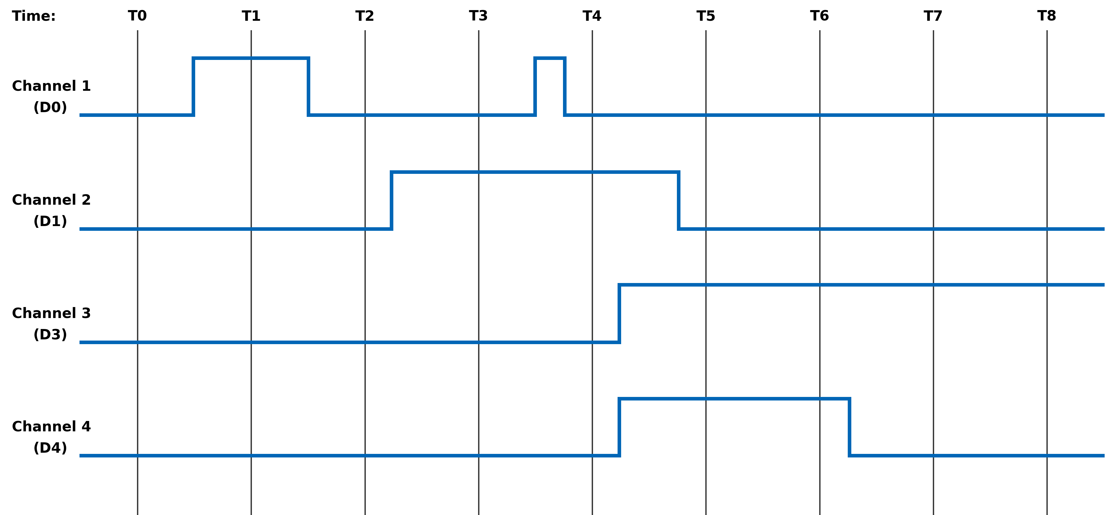
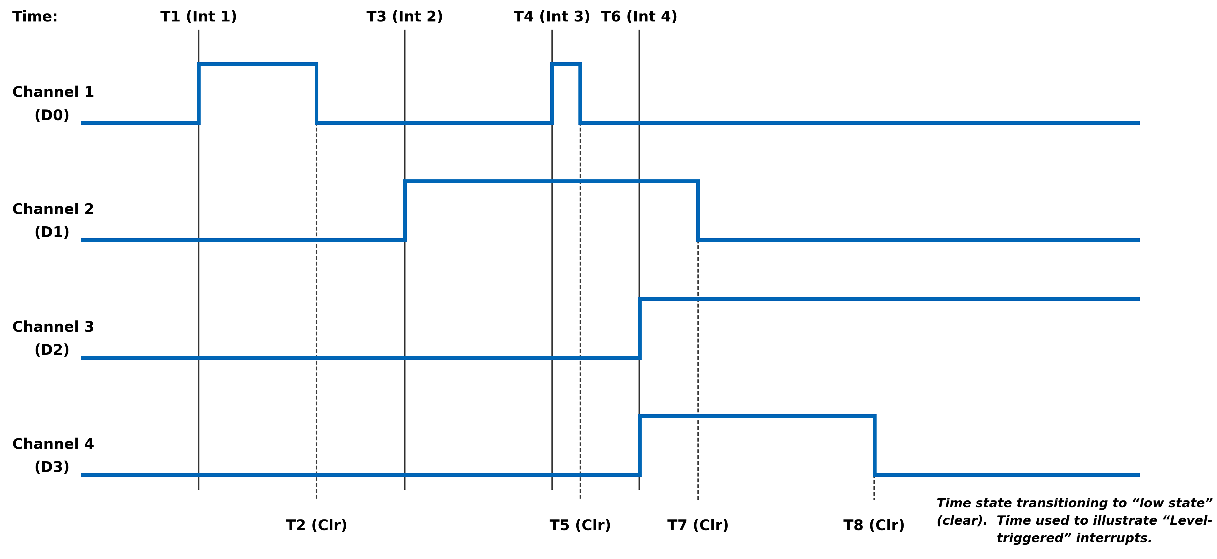
Appendix B: User Watchdog Timer Functionality
Principle of Operation
The User Watchdog Timer is optionally activated by the applications that require the module’s outputs to be disabled as a failsafe in the event of an application failure or crash. The circuit is designed such that a specific periodic write strobe pattern must be executed by the software to maintain operation and prevent the disablement from taking place.
The User Watchdog Timer is inactive until the application sends an initial strobe by writing the value 0x55AA to the UWDT Strobe register. After activating the User Watchdog Timer, the application must continually strobe the timer within the intervals specified with the configurable UWDT Quiet Time and UWDT Window registers. The timing of the strobes must be consistent with the following rules:
The application must not strobe during the Quiet time.
The application must strobe within the Window time.
The application must not strobe more than once in a single window time.
A violation of any of these rules will trigger a User Watchdog Timer fault and result in shutting down any isolated power supplies and/or disabling any active drive outputs, as applicable for the specific module. Upon a User Watchdog Timer event, recovery to the module shutting down will require the module to be reset.
Figure 20 and Figure 21 provides an overview and an example with actual values for the User Watchdog Timer Strobes, Quiet Time and Window. As depicted in the diagrams, there are two processes that run in parallel. The Strobe event starts the timer for the beginning of the “Quiet Time”. The timer for the Previous Strobe event continues to run to ensure that no additional Strobes are received within the “Window” associated with the Previous Strobe.
The optimal target for the user watchdog strobes should be at the interval of [Quiet time + ½ Window time] after the previous strobe, which will place the strobe in the center of the window. This affords the greatest margin of safety against unintended disablement in critical operations.
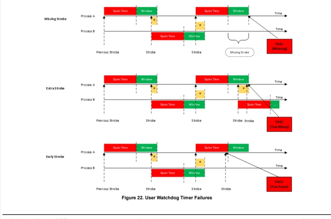
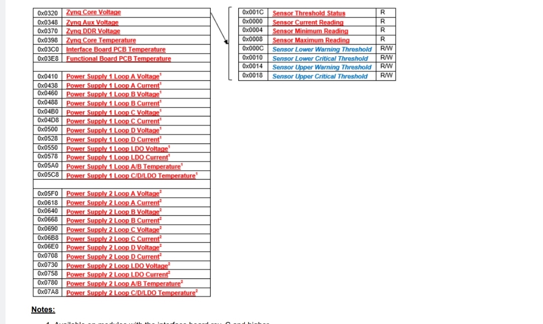
IMAGE68DT1/68DT1-Img33.jpg[]
Register Descriptions
The register descriptions provide the register name, Type, Data Range, Read or Write information, Initialized Value, and a description of the function.
User Watchdog Timer Registers
The registers associated with the User Watchdog Timer provide the ability to specify the UWDT Quiet Time and the UWDT Window that will be monitored to ensure that EXACTLY ONE User Watchdog Timer (UWDT) Strobe is written within the window.
UWDT Quiet Time
Function: Sets Quiet Time value (in microseconds) to use for the User Watchdog Timer Frame.
Type: unsigned binary word (32-bit)
Data Range: 0 µsec to 2^32 µsec (0x0 to 0xFFFFFFFF)
Read/Write: R/W
Initialized Value: 0x0
Operational Settings*: LSB = 1 µsec. The application must NOT write a strobe in the time between the previous strobe and the end of the Quiet time interval. In addition, the application must write in the UWDT Window EXACTLY ONCE.
UWDT Window
Function: Sets Window value (in microseconds) to use for the User Watchdog Timer Frame.
Type: unsigned binary word (32-bit)
Data Range: 0 µsec to 2^32 µsec (0x0 to 0xFFFFFFFF)
Read/Write: R/W
Initialized Value: 0x0
Operational Settings: LSB = 1 µsec. The application must write the strobe once within the Window time after the end of the Quiet time interval. The application must write in the UWDT Window EXACTLY ONCE. This setting must be initialized to a non-zero value for operation and should allow sufficient tolerance for strobe timing by the application.
UWDT Strobe
Function: Writes the strobe value to be use for the User Watchdog Timer Frame.
Type: unsigned binary word (32-bit)
Data Range: 0x55AA
Read/Write: W
Initialized Value: 0x0
Operational Settings: At startup, the user watchdog is disabled. Write the value of 0x55AA to this register to start the user watchdog timer monitoring after initial power on or a reset. To prevent a disablement, the application must periodically write the strobe based on the user watchdog timer rules.
Status and Interrupt
The modules that are capable of User Watchdog Timer support provide status registers for the User Watchdog Timer.
User Watchdog Timer Status
The status register that contains the User Watchdog Timer Fault information is also used to indicate channel Inter-FPGA failures on modules that have communication between FPGA components. There are four registers associated with the User Watchdog Timer Fault/Inter-FPGA Failure Status: Dynamic, Latched, Interrupt Enable, and Set Edge/Level Interrupt.
User Watchdog Timer Fault/Inter-FPGA Failure Dynamic Status User Watchdog Timer Fault/Inter-FPGA Failure Latched Status User Watchdog Timer Fault/Inter-FPGA Failure Interrupt Enable User Watchdog Timer Fault/Inter-FPGA Failure Set Edge/Level Interrupt
| Bit(s) | Status | Description |
|---|---|---|
| D31 | User Watchdog Timer Fault Status | 0 = No Fault 1 = User Watchdog Timer Fault |
| D30:D0 | Reserved for Inter-FPGA Failure Status | Channel bit-mapped indicating channel interFPGA communication failure detection. |
Function: Sets the corresponding bit (D31) associated with the channel’s User Watchdog Timer Fault error.
Type: unsigned binary word (32-bit)
Data Range: 0x0000 0000 to 0xFFFF FFFF
Read/Write: R (Dynamic), R/W (Latched, Interrupt Enable, Edge/Level Interrupt)
Initialized Value: 0
Function Register Map
Key: Bold Italic = Configuration/Control Bold Underline = Status
*When an event is detected, the bit associated with the event is set in this register and will remain set until the user clears the event bit. Clearing the bit requires writing a 1 back to the specific bit that was set when read (i.e. write-1-toclear, writing a ‘1’ to a bit set to ‘1’ will set the bit to ‘0’).
User Watchdog Timer Registers
| 0x01C0 | UWDT Quiet Time | R/W |
|---|---|---|
| 0x01C4 | UWDT Window | R/W |
| 0x01C8 | UWDT Strobe | W |
Status Registers
User Watchdog Timer Fault/Inter-FPGA Failure*
| 0x0880 | Dynamic Status Ch 1-24 | R |
|---|---|---|
| 0x0884 | Latched Status Ch 1-24* | R/W |
| 0x0888 | Interrupt Enable Ch 1-24 | R/W |
| 0x088C | Set Edge/Level Interrupt Ch 1-24 | R/W |
| 0x0980 | Dynamic Status Ch 25-48 | R |
|---|---|---|
| 0x0984 | Latched Status Ch 25-48* | R/W |
| 0x0988 | Interrupt Enable Ch 25-48 | R/W |
| 0x098C | Set Edge/Level Interrupt Ch 25-48 | R/W |
| 0x0A80 | Dynamic Status Ch 49-72 | R |
|---|---|---|
| 0x0A84 | Latched Status Ch 49-72* | R/W |
| 0x0A88 | Interrupt Enable Ch 49-72 | R/W |
| 0x0A8C | Set Edge/Level Interrupt Ch 49-72 | R/W |
| 0x0B80 | Dynamic Status Ch 73-96 | R |
|---|---|---|
| 0x0B84 | Latched Status Ch 73-96* | R/W |
| 0x0B88 | Interrupt Enable Ch 73-96 | R/W |
| 0x0B8C | Set Edge/Level Interrupt Ch 73-96 | R/W |
APPENDIX D: MODULE COMMON REGISTERS
MODULE COMMON REGISTERS
The registers described in this document are common to all NAI Generation 5 modules.
Module Information Registers
The registers in this section provide module information such as firmware revisions, capabilities and unique serial number information.
FPGA Version Registers
The FPGA firmware version registers include registers that contain the Revision, Compile Timestamp, SerDes Revision, Template Revision and Zynq Block Revision information.
FPGA Revision Function: FPGA firmware revision Type: unsigned binary word (32-bit) Data Range: 0x0000 0000 to 0xFFFF FFFF Read/Write: R Initialized Value: Value corresponding to the revision of the board's FPGA Operational Settings: The upper 16-bits are the major revision and the lower 16-bits are the minor revision.
D31 D30 D29 D28 D27 D26 D25 D24 D23 D22 D21 D20 D19 D18 D17 D16 Major Revision Number D15 D14 D13 D12 D11 D10 D9 D8 D7 D6 D5 D4 D3 D2 D1 D0 Minor Revision Number
FPGA Compile Timestamp Function: Compile Timestamp for the FPGA firmware. Type: unsigned binary word (32-bit) Data Range: N/A Read/Write: R Initialized Value: Value corresponding to the compile timestamp of the board's FPGA Operational Settings: The 32-bit value represents the Day, Month, Year, Hour, Minutes and Seconds as formatted in the table:
D31 D30 D29 D28 D27 D26 D25 D24 D23 D22 D21 D20 D19 D18 D17 D16 day (5-bits) month (4-bits) year (6-bits) hr D15 D14 D13 D12 D11 D10 D9 D8 D7 D6 D5 D4 D3 D2 D1 D0 hour (5-bits) minutes (6-bits) seconds (6-bits)
FPGA SerDes Revision Function: FPGA SerDes revision Type: unsigned binary word (32-bit) Data Range: 0x0000 0000 to 0xFFFF FFFF Read/Write: R Initialized Value: Value corresponding to the SerDes revision of the board's FPGA Operational Settings: The upper 16-bits are the major revision, and the lower 16-bits are the minor revision.
D31 D30 D29 D28 D27 D26 D25 D24 D23 D22 D21 D20 D19 D18 D17 D16 Major Revision Number D15 D14 D13 D12 D11 D10 D9 D8 D7 D6 D5 D4 D3 D2 D1 D0 Minor Revision Number
FPGA Template Revision Function: FPGA Template revision Type: unsigned binary word (32-bit) Data Range: 0x0000 0000 to 0xFFFF FFFF Read/Write: R Initialized Value: Value corresponding to the template revision of the board's FPGA Operational Settings: The upper 16-bits are the major revision, and the lower 16-bits are the minor revision.
D31 D30 D29 D28 D27 D26 D25 D24 D23 D22 D21 D20 D19 D18 D17 D16 Major Revision Number D15 D14 D13 D12 D11 D10 D9 D8 D7 D6 D5 D4 D3 D2 D1 D0 Minor Revision Number
FPGA Zynq Block Revision Function: FPGA Zynq Block revision Type: unsigned binary word (32-bit) Data Range: 0x0000 0000 to 0xFFFF FFFF Read/Write: R Initialized Value: Value corresponding to the Zynq block revision of the board's FPGA Operational Settings: The upper 16-bits are the major revision, and the lower 16-bits are the minor revision.
D31 D30 D29 D28 D27 D26 D25 D24 D23 D22 D21 D20 D19 D18 D17 D16 Major Revision Number D15 D14 D13 D12 D11 D10 D9 D8 D7 D6 D5 D4 D3 D2 D1 D0 Minor Revision Number Bare Metal Version Registers
The Bare Metal firmware version registers include registers that contain the Revision and Compile Time information.
Bare Metal Revision Function: Bare Metal firmware revision Type: unsigned binary word (32-bit) Data Range: 0x0000 0000 to 0xFFFF FFFF Read/Write: R Initialized Value: Value corresponding to the revision of the board's Bare Metal Operational Settings: The upper 16-bits are the major revision and the lower 16-bits are the minor revision.
D31 D30 D29 D28 D27 D26 D25 D24 D23 D22 D21 D20 D19 D18 D17 D16 Major Revision Number D15 D14 D13 D12 D11 D10 D9 D8 D7 D6 D5 D4 D3 D2 D1 D0 Minor Revision Number
Bare Metal Compile Time Function: Provides an ASCII representation of the Date/Time for the Bare Metal compile time. Type: 24-character ASCII string - Six (6) unsigned binary word (32-bit) Data Range: N/A Read/Write: R Initialized Value: Value corresponding to the ASCII representation of the compile time of the board's Bare Metal Operational Settings: The six 32-bit words provide an ASCII representation of the Date/Time. The hexadecimal values in the field below represent: May 17 2019 at 15:38:32 Note
little-endian order of ASCII values
Word 1 (Ex. 0x2079614D) D31 D30 D29 D28 D27 D26 D25 D24 D23 D22 D21 D20 D19 D18 D17 D16 Space (0x20) Month ('y' - 0x79) D15 D14 D13 D12 D11 D10 D9 D8 D7 D6 D5 D4 D3 D2 D1 D0 Month ('a' - 0x61) Month ('M' - 0x4D) Word 2 (Ex. 0x32203731) D31 D30 D29 D28 D27 D26 D25 D24 D23 D22 D21 D20 D19 D18 D17 D16 Year ('2' - 0x32) Space (0x20) D15 D14 D13 D12 D11 D10 D9 D8 D7 D6 D5 D4 D3 D2 D1 D0 Day ('7' - 0x37) Day ('1' - 0x31) Word 3 (Ex. 0x20393130) D31 D30 D29 D28 D27 D26 D25 D24 D23 D22 D21 D20 D19 D18 D17 D16 Space (0x20) Year ('9' - 0x39) D15 D14 D13 D12 D11 D10 D9 D8 D7 D6 D5 D4 D3 D2 D1 D0 Year ('1' - 0x31) Year ('0' - 0x30) Word 4 (Ex. 0x31207461) D31 D30 D29 D28 D27 D26 D25 D24 D23 D22 D21 D20 D19 D18 D17 D16 Hour ('1' - 0x31) Space (0x20) D15 D14 D13 D12 D11 D10 D9 D8 D7 D6 D5 D4 D3 D2 D1 D0 'a' (0x74) 't' (0x61) Word 5 (Ex. 0x38333A35) D31 D30 D29 D28 D27 D26 D25 D24 D23 D22 D21 D20 D19 D18 D17 D16 Minute ('8' - 0x38) Minute ('3' - 0x33) D15 D14 D13 D12 D11 D10 D9 D8 D7 D6 D5 D4 D3 D2 D1 D0 ':' (0x3A) Hour ('5' - 0x35) Word 6 (Ex. 0x0032333A) D31 D30 D29 D28 D27 D26 D25 D24 D23 D22 D21 D20 D19 D18 D17 D16 NULL (0x00) Seconds ('2' - 0x32) D15 D14 D13 D12 D11 D10 D9 D8 D7 D6 D5 D4 D3 D2 D1 D0 Seconds ('3' - 0x33) ':' (0x3A) FSBL Version Registers
The FSBL version registers include registers that contain the Revision and Compile Time information for the First Stage Boot Loader (FSBL).
FSBL Revision Function: FSBL firmware revision Type: unsigned binary word (32-bit) Data Range: 0x0000 0000 to 0xFFFF FFFF Read/Write: R Initialized Value: Value corresponding to the revision of the board's FSBL Operational Settings: The upper 16-bits are the major revision, and the lower 16-bits are the minor revision.
D31 D30 D29 D28 D27 D26 D25 D24 D23 D22 D21 D20 D19 D18 D17 D16 Major Revision Number D15 D14 D13 D12 D11 D10 D9 D8 D7 D6 D5 D4 D3 D2 D1 D0 Minor Revision Number
FSBL Compile Time Function: Provides an ASCII representation of the Date/Time for the FSBL compile time. Type: 24-character ASCII string - Six (6) unsigned binary word (32-bit) Data Range: N/A Read/Write: R Initialized Value: Value corresponding to the ASCII representation of the Compile Time of the board's FSBL Operational Settings: The six 32-bit words provide an ASCII representation of the Date/Time. The hexadecimal values in the field below represent: May 17 2019 at 15:38:32
Note
little-endian order of ASCII values
Word 1 (Ex. 0x2079614D) D31 D30 D29 D28 D27 D26 D25 D24 D23 D22 D21 D20 D19 D18 D17 D16 Space (0x20) Month ('y' - 0x79) D15 D14 D13 D12 D11 D10 D9 D8 D7 D6 D5 D4 D3 D2 D1 D0 Month ('a' - 0x61) Month ('M' - 0x4D) Word 2 (Ex. 0x32203731) D31 D30 D29 D28 D27 D26 D25 D24 D23 D22 D21 D20 D19 D18 D17 D16 Year ('2' - 0x32) Space (0x20) D15 D14 D13 D12 D11 D10 D9 D8 D7 D6 D5 D4 D3 D2 D1 D0 Day ('7' - 0x37) Day ('1' - 0x31) Word 3 (Ex. 0x20393130) D31 D30 D29 D28 D27 D26 D25 D24 D23 D22 D21 D20 D19 D18 D17 D16 Space (0x20) Year ('9' - 0x39) D15 D14 D13 D12 D11 D10 D9 D8 D7 D6 D5 D4 D3 D2 D1 D0 Year ('1' - 0x31) Year ('0' - 0x30) Word 4 (Ex. 0x31207461) D31 D30 D29 D28 D27 D26 D25 D24 D23 D22 D21 D20 D19 D18 D17 D16 Hour ('1' - 0x31) Space (0x20) D15 D14 D13 D12 D11 D10 D9 D8 D7 D6 D5 D4 D3 D2 D1 D0 'a' (0x74) 't' (0x61) Word 5 (Ex. 0x38333A35) D31 D30 D29 D28 D27 D26 D25 D24 D23 D22 D21 D20 D19 D18 D17 D16 Minute ('8' - 0x38) Minute ('3' - 0x33) D15 D14 D13 D12 D11 D10 D9 D8 D7 D6 D5 D4 D3 D2 D1 D0 ':' (0x3A) Hour ('5' - 0x35) Word 6 (Ex. 0x0032333A) D31 D30 D29 D28 D27 D26 D25 D24 D23 D22 D21 D20 D19 D18 D17 D16 NULL (0x00) Seconds ('2' - 0x32) D15 D14 D13 D12 D11 D10 D9 D8 D7 D6 D5 D4 D3 D2 D1 D0 Seconds ('3' - 0x33) ':' (0x3A) Module Serial Number Registers
The Module Serial Number registers include registers that contain the Serial Numbers for the Interface Board and the Functional Board of the module.
Interface Board Serial Number Function: Unique 128-bit identifier used to identify the interface board. Type: 16-character ASCII string - Four (4) unsigned binary words (32-bit) Data Range: N/A Read/Write: R Initialized Value: Serial number of the interface board Operational Settings: This register is for information purposes only.
Functional Board Serial Number Function: Unique 128-bit identifier used to identify the functional board. Type: 16-character ASCII string - Four (4) unsigned binary words (32-bit) Data Range: N/A Read/Write: R Initialized Value: Serial number of the functional board Operational Settings: This register is for information purposes only.
Module Capability Function: Provides indication for whether or not the module can support the following: SerDes block reads, SerDes FIFO block reads, SerDes packing (combining two 16-bit values into one 32-bit value) and floating point representation. The purpose for block access and packing is to improve the performance of accessing larger amounts of data over the SerDes interface. Type: unsigned binary word (32-bit) Data Range: 0x0000 0000 to 0x0000 0107 Read/Write: R Initialized Value: 0x0000 0107 Operational Settings: A “1” in the bit associated with the capability indicates that it is supported.
D31 D30 D29 D28 D27 D26 D25 D24 D23 D22 D21 D20 D19 D18 D17 D16 0 0 0 0 0 0 0 0 0 0 0 0 0 0 0 0 D15 D14 D13 D12 D11 D10 D9 D8 D7 D6 D5 D4 D3 D2 D1 D0 0 0 0 0 0 0 0 Flt-Pt 0 0 0 0 0 Pack FIFO Blk Blk
Module Memory Map Revision Function: Module Memory Map revision Type: unsigned binary word (32-bit) Data Range: 0x0000 0000 to 0xFFFF FFFF Read/Write: R Initialized Value: Value corresponding to the Module Memory Map Revision Operational Settings: The upper 16-bits are the major revision and the lower 16-bits are the minor revision.
D31 D30 D29 D28 D27 D26 D25 D24 D23 D22 D21 D20 D19 D18 D17 D16 Major Revision Number D15 D14 D13 D12 D11 D10 D9 D8 D7 D6 D5 D4 D3 D2 D1 D0 Minor Revision Number Module Measurement Registers
The registers in this section provide module temperature measurement information.
Temperature Readings Registers
The temperature registers provide the current, maximum (from power-up) and minimum (from power-up) Zynq and PCB temperatures.
Interface Board Current Temperature Function: Measured PCB and Zynq Core temperatures on Interface Board. Type: signed byte (8-bits) for PCB and signed byte (8-bits) for Zynq core temperatures Data Range: 0x0000 0000 to 0x0000 FFFF Read/Write: R Initialized Value: Value corresponding to the measured PCB and Zynq core temperatures based on the table below Operational Settings: The upper 16-bits are not used, and the lower 16-bits are the PCB and Zynq Core Temperatures. For example, if the register contains the value 0x0000 202C, this represents PCB Temperature = 32° Celsius and Zynq Temperature = 44° Celsius.
D31 D30 D29 D28 D27 D26 D25 D24 D23 D22 D21 D20 D19 D18 D17 D16 0 0 0 0 0 0 0 0 0 0 0 0 0 0 0 0 D15 D14 D13 D12 D11 D10 D9 D8 D7 D6 D5 D4 D3 D2 D1 D0 PCB Temperature Zynq Core Temperature
Functional Board Current Temperature Function: Measured PCB temperature on Functional Board. Type: signed byte (8-bits) for PCB Data Range: 0x0000 0000 to 0x0000 00FF Read/Write: R Initialized Value: Value corresponding to the measured PCB on the table below Operational Settings: The upper 24-bits are not used, and the lower 8-bits are the PCB Temperature. For example, if the register contains the value 0x0000 0019, this represents PCB Temperature = 25° Celsius.
D31 D30 D29 D28 D27 D26 D25 D24 D23 D22 D21 D20 D19 D18 D17 D16 0 0 0 0 0 0 0 0 0 0 0 0 0 0 0 0 D15 D14 D13 D12 D11 D10 D9 D8 D7 D6 D5 D4 D3 D2 D1 D0 0 0 0 0 0 0 0 0 PCB Temperature
Interface Board Maximum Temperature Function: Maximum PCB and Zynq Core temperatures on Interface Board since power-on. Type: signed byte (8-bits) for PCB and signed byte (8-bits) for Zynq core temperatures Data Range: 0x0000 0000 to 0x0000 FFFF Read/Write: R Initialized Value: Value corresponding to the maximum measured PCB and Zynq core temperatures since power-on based on the table below Operational Settings: The upper 16-bits are not used, and the lower 16-bits are the maximum PCB and Zynq Core Temperatures. For example, if the register contains the value 0x0000 5569, this represents maximum PCB Temperature = 85° Celsius and maximum Zynq Temperature = 105° Celsius.
D31 D30 D29 D28 D27 D26 D25 D24 D23 D22 D21 D20 D19 D18 D17 D16 0 0 0 0 0 0 0 0 0 0 0 0 0 0 0 0 D15 D14 D13 D12 D11 D10 D9 D8 D7 D6 D5 D4 D3 D2 D1 D0 PCB Temperature Zynq Core Temperature
Interface Board Minimum Temperature Function: Minimum PCB and Zynq Core temperatures on Interface Board since power-on. Type: signed byte (8-bits) for PCB and signed byte (8-bits) for Zynq core temperatures Data Range: 0x0000 0000 to 0x0000 FFFF Read/Write: R Initialized Value: Value corresponding to the minimum measured PCB and Zynq core temperatures since power-on based on the table below Operational Settings: The upper 16-bits are not used, and the lower 16-bits are the minimum PCB and Zynq Core Temperatures. For example, if the register contains the value 0x0000 D8E7, this represents minimum PCB Temperature = -40° Celsius and minimum Zynq Temperature = -25° Celsius.
D31 D30 D29 D28 D27 D26 D25 D24 D23 D22 D21 D20 D19 D18 D17 D16 0 0 0 0 0 0 0 0 0 0 0 0 0 0 0 0 D15 D14 D13 D12 D11 D10 D9 D8 D7 D6 D5 D4 D3 D2 D1 D0 PCB Temperature Zynq Core Temperature
Functional Board Maximum Temperature Function: Maximum PCB temperature on Functional Board since power-on. Type: signed byte (8-bits) for PCB Data Range: 0x0000 0000 to 0x0000 00FF Read/Write: R Initialized Value: Value corresponding to the measured PCB on the table below Operational Settings: The upper 24-bits are not used, and the lower 8-bits are the PCB Temperature. For example, if the register contains the value 0x0000 0055, this represents PCB Temperature = 85° Celsius.
D31 D30 D29 D28 D27 D26 D25 D24 D23 D22 D21 D20 D19 D18 D17 D16 0 0 0 0 0 0 0 0 0 0 0 0 0 0 0 0 D15 D14 D13 D12 D11 D10 D9 D8 D7 D6 D5 D4 D3 D2 D1 D0 0 0 0 0 0 0 0 0 PCB Temperature
Functional Board Minimum Temperature Function: Minimum PCB temperature on Functional Board since power-on. Type: signed byte (8-bits) for PCB Data Range: 0x0000 0000 to 0x0000 00FF Read/Write: R Initialized Value: Value corresponding to the measured PCB on the table below Operational Settings: The upper 24-bits are not used, and the lower 8-bits are the PCB Temperature. For example, if the register contains the value 0x0000 00D8, this represents PCB Temperature = -40° Celsius.
D31 D30 D29 D28 D27 D26 D25 D24 D23 D22 D21 D20 D19 D18 D17 D16 0 0 0 0 0 0 0 0 0 0 0 0 0 0 0 0 D15 D14 D13 D12 D11 D10 D9 D8 D7 D6 D5 D4 D3 D2 D1 D0 0 0 0 0 0 0 0 0 PCB Temperature Higher Precision Temperature Readings Registers
These registers provide higher precision readings of the current Zynq and PCB temperatures.
Higher Precision Zynq Core Temperature Function: Higher precision measured Zynq Core temperature on Interface Board. Type: signed word (16-bits) for integer part and unsigned word (16-bits) for fractional part Data Range: 0x0000 0000 to 0xFFFF FFFF Read/Write: R Initialized Value: Measured Zynq Core temperature on Interface Board Operational Settings: The upper 16-bits represent the signed integer part of the temperature and the lower 16-bits represent the fractional part of the temperature with the resolution of 1/1000 of degree Celsius. For example, if the register contains the value 0x002B 0271, this represents Zynq Core Temperature = 43.625° Celsius, and value 0xFFF6 0177 represents -10.375° Celsius.
D31 D30 D29 D28 D27 D26 D25 D24 D23 D22 D21 D20 D19 D18 D17 D16 Signed Integer Part of Temperature D15 D14 D13 D12 D11 D10 D9 D8 D7 D6 D5 D4 D3 D2 D1 D0 Fractional Part of Temperature
Higher Precision Interface PCB Temperature Function: Higher precision measured Interface PCB temperature. Type: signed word (16-bits) for integer part and unsigned word (16-bits) for fractional part Data Range: 0x0000 0000 to 0xFFFF FFFF Read/Write: R Initialized Value: Measured Interface PCB temperature Operational Settings: The upper 16-bits represent the signed integer part of the temperature and the lower 16-bits represent the fractional part of the temperature with the resolution of 1/1000 of degree Celsius. For example, if the register contains the value 0x0020 007D, this represents Interface PCB Temperature = 32.125° Celsius, and value 0xFFE8 036B represents -24.875° Celsius.
D31 D30 D29 D28 D27 D26 D25 D24 D23 D22 D21 D20 D19 D18 D17 D16 Signed Integer Part of Temperature D15 D14 D13 D12 D11 D10 D9 D8 D7 D6 D5 D4 D3 D2 D1 D0 Fractional Part of Temperature
Higher Precision Functional PCB Temperature Function: Higher precision measured Functional PCB temperature. Type: signed word (16-bits) for integer part and unsigned word (16-bits) for fractional part Data Range: 0x0000 0000 to 0xFFFF FFFF Read/Write: R Initialized Value: Measured Functional PCB temperature Operational Settings: The upper 16-bits represent the signed integer part of the temperature and the lower 16-bits represent the fractional part of the temperature with the resolution of 1/100 of degree Celsius. For example, if the register contains the value 0x0018 004B, this represents Functional PCB Temperature = 24.75° Celsius, and value 0xFFD9 0019 represents -39.25° Celsius.
D31 D30 D29 D28 D27 D26 D25 D24 D23 D22 D21 D20 D19 D18 D17 D16 Signed Integer Part of Temperature D15 D14 D13 D12 D11 D10 D9 D8 D7 D6 D5 D4 D3 D2 D1 D0 Fractional Part of Temperature Module Health Monitoring Registers
The registers in this section provide module temperature measurement information. If the temperature measurements reaches the Lower Critical or Upper Critical conditions, the module will automatically reset itself to prevent damage to the hardware.
Module Sensor Summary Status Function: The corresponding sensor bit is set if the sensor has crossed any of its thresholds. Type: unsigned binary word (32-bits) Data Range: See table below Read/Write: R Initialized Value: 0 Operational Settings: This register provides a summary for module sensors. When the corresponding sensor bit is set, the Sensor Threshold Status register for that sensor will indicate the threshold condition that triggered the event.
Bit(s) Sensor D31:D6 Reserved D5 Functional Board PCB Temperature D4 Interface Board PCB Temperature D3:D0 Reserved Module Sensor Registers
The registers listed in this section apply to each module sensor listed for the Module Sensor Summary Status register. Each individual sensor register provides a group of registers for monitoring module temperatures readings. From these registers, a user can read the current temperature of the sensor in addition to the minimum and maximum temperature readings since power-up. Upper and lower critical/warning temperature thresholds can be set and monitored from these registers. When a programmed temperature threshold is crossed, the Sensor Threshold Status register will set the corresponding bit for that threshold. The figure below shows the functionality of this group of registers when accessing the Interface Board PCB Temperature sensor as an example.
Sensor Threshold Status Function: Reflects which threshold has been crossed Type: unsigned binary word (32-bits) Data Range: See table below Read/Write: R Initialized Value: 0 Operational Settings: The associated bit is set when the sensor reading exceed the corresponding threshold settings.
Bit(s) Description D31:D4 Reserved D3 Exceeded Upper Critical Threshold D2 Exceeded Upper Warning Threshold D1 Exceeded Lower Critical Threshold D0 Exceeded Lower Warning Threshold
Sensor Current Reading Function: Reflects current reading of temperature sensor Type: Single Precision Floating Point Value (IEEE-754) Data Range: Single Precision Floating Point Value (IEEE-754) Read/Write: R Initialized Value: N/A Operational Settings: The register represents current sensor reading as a single precision floating point value. For example, for a temperature sensor, register value 0x41C6 0000 represents temperature = 24.75° Celsius.
Sensor Minimum Reading Function: Reflects minimum value of temperature sensor since power up Type: Single Precision Floating Point Value (IEEE-754) Data Range: Single Precision Floating Point Value (IEEE-754) Read/Write: R Initialized Value: N/A Operational Settings: The register represents minimum sensor value as a single precision floating point value. For example, for a temperature sensor, register value 0x41C6 0000 represents temperature = 24.75° Celsius.
Sensor Maximum Reading Function: Reflects maximum value of temperature sensor since power up Type: Single Precision Floating Point Value (IEEE-754) Data Range: Single Precision Floating Point Value (IEEE-754) Read/Write: R Initialized Value: N/A Operational Settings: The register represents maximum sensor value as a single precision floating point value. For example, for a temperature sensor, register value 0x41C6 0000 represents temperature = 24.75° Celsius.
Sensor Lower Warning Threshold Function: Reflects lower warning threshold of temperature sensor Type: Single Precision Floating Point Value (IEEE-754) Data Range: Single Precision Floating Point Value (IEEE-754) Read/Write: R/W Initialized Value: Default lower warning threshold (value dependent on specific sensor) Operational Settings: The register represents sensor lower warning threshold as a single precision floating point value. For example, for a temperature sensor, register value 0xC220 0000 represents temperature = -40.0° Celsius.
Sensor Lower Critical Threshold Function: Reflects lower critical threshold of temperature sensor Type: Single Precision Floating Point Value (IEEE-754) Data Range: Single Precision Floating Point Value (IEEE-754) Read/Write: R/W Initialized Value: Default lower critical threshold (value dependent on specific sensor) Operational Settings: The register represents sensor lower critical threshold as a single precision floating point value. For example, for a temperature sensor, register value 0xC25C 0000 represents temperature = -55.0° Celsius.
Sensor Upper Warning Threshold Function: Reflects upper warning threshold of temperature sensor Type: Single Precision Floating Point Value (IEEE-754) Data Range: Single Precision Floating Point Value (IEEE-754) Read/Write: R/W Initialized Value: Default upper warning threshold (value dependent on specific sensor) Operational Settings: The register represents sensor upper warning threshold as a single precision floating point value. For example, for a temperature sensor, register value 0x42AA 0000 represents temperature = 85.0° Celsius.
Sensor Upper Critical Threshold Function: Reflects upper critical threshold of temperature sensor Type: Single Precision Floating Point Value (IEEE-754) Data Range: Single Precision Floating Point Value (IEEE-754) Read/Write: R/W Initialized Value: Default upper critical threshold (value dependent on specific sensor) Operational Settings: The register represents sensor upper critical threshold as a single precision floating point value. For example, for a temperature sensor, register value 0x42FA 0000 represents temperature = 125.0° Celsius. FUNCTION REGISTER MAP
KEY
Configuration/Control Measurement/Status/Board Information
MODULE INFORMATION REGISTERS OFFSET REGISTER NAME ACCESS OFFSET REGISTER NAME ACCESS 0x003C FPGA Revision R 0x0074 Bare Metal Revision R 0x0030 FPGA Compile Timestamp R 0x0080 Bare Metal Compile Time (Bit 0-31) R 0x0034 FPGA SerDes Revision R 0x0084 Bare Metal Compile Time (Bit 32-63) R 0x0038 FPGA Template Revision R 0x0088 Bare Metal Compile Time (Bit 64-95) R 0x0040 FPGA Zynq Block Revision R 0x008C Bare Metal Compile Time (Bit 96-127) R 0x0090 Bare Metal Compile Time (Bit 128-159) R 0x0094 Bare Metal Compile Time (Bit 160-191) R 0x007C FSBL Revision R 0x00B0 FSBL Compile Time (Bit 0-31) R 0x00B4 FSBL Compile Time (Bit 32-63) R 0x00B8 FSBL Compile Time (Bit 64-95) R 0x00BC FSBL Compile Time (Bit 96-127) R 0x00C0 FSBL Compile Time (Bit 128-159) R 0x00C4 FSBL Compile Time (Bit 160-191) R 0x0000 Interface Board Serial Number (Bit 0-31) R 0x0010 Functional Board Serial Number (Bit 0-31) R 0x0034 Interface Board Serial Number (Bit 32-63) R 0x0014 Functional Board Serial Number (Bit 32-63) R 0x0008 Interface Board Serial Number (Bit 64-95) R 0x0018 Functional Board Serial Number (Bit 64-95) R 0x000C Interface Board Serial Number (Bit 96-127) R 0x001C Functional Board Serial Number (Bit 96-127) R 0x0070 Module Capability R 0x01FC Module Memory Map Revision R
MODULE MEASUREMENTS REGISTERS OFFSET REGISTER NAME ACCESS OFFSET REGISTER NAME ACCESS 0x0200 Interface Board PCB/Zynq Current Temp R 0x0208 Functional Board PCB Current Temp R 0x0218 Interface Board PCB/Zynq Max Temp R 0x0228 Functional Board PCB Max Temp R 0x0220 Interface Board PCB/Zynq Min Temp R 0x0230 Functional Board PCB Min Temp R 0x02C0 Higher Precision Zynq Core Temperature R 0x02C4 Higher Precision Interface PCB Temperature R 0x02E0 Higher Precision Functional PCB Temperature R
MODULE HEALTH MONITORING REGISTERS OFFSET REGISTER NAME ACCESS OFFSET REGISTER NAME ACCESS 0x07F8 Module Sensor Summary Status R
REVISION HISTORY
Motherboard Manual - Module Common Registers Revision History Revision Revision Date Description C 2023-08-11 ECO C10649, initial release of module common registers manual. C1 2024-05-15 ECO C11522, removed Zynq Core/Aux/DDR Voltage register descriptions from Module Measurement Registers. Pg.16, updated Module Sensor Summary Status register to add PS references; updated Bit Table to change voltage/current bits to 'reserved'. Pg.16, updated Module/Power Supply Sensor Registers description to better describe register functionality and to add figure. Pg.17, added 'Exceeded' to threshold bit descriptions. Pg.17-18, removed voltage/current references from sensor descriptions. Pg.20, removed Zynq Core/Aux/DDR Voltage register offsets from Module Measurement Registers. Pg.20, updated Module Health Monitoring Registers offset tables. C2 2024-07-10 ECO C11701, pg.16, updated Module Sensor Summary Status register to remove PS references;updated Bit Table to change PS temperature bits to 'reserved'. Pg.16, updated Module SensorRegisters description to remove PS references. Pg.20, updated Module Health MonitoringRegisters offset tables to remove PS temperature register offsets. Link to original
DOCS.NAII REVISIONS Revision Date Description 2025-11-05 Corrected register offsets for Interface Board Min Temp and Function Board Min & Max Temps. 2026-03-02 Formatting updates to document; no technical changes. 2026-05-20 Minor formatting fixes (non-technical changes). 2026-07-15 Updated images for online quality; minor additional formatting updates (no technical changes).


FUNCTION REGISTER MAP
Key: Bold Underline = Measurement/Status Bold Italic = Configuration/Control
Module Information Registers
| 0x003C | FPGA Revision | R |
|---|---|---|
| 0x0030 | FPGA Compile Timestamp | R |
| 0x0034 | FPGA SerDes Revision | R |
| 0x0038 | FPGA Template Revision | R |
| 0x0040 | FPGA Zynq Block Revision | R |
| 0x0074 | Bare Metal Revision | R |
|---|---|---|
| 0x0080 | Bare Metal Compile Time (Bit 0-31) | R |
| 0x0084 | Bare Metal Compile Time (Bit 32-63) | R |
| 0x0088 | Bare Metal Compile Time (Bit 64-95) | R |
| 0x008C | Bare Metal Compile Time (Bit 96-127) | R |
| 0x0090 | Bare Metal Compile Time (Bit 128-159) | R |
| 0x0094 | Bare Metal Compile Time (Bit 160-191) | R |
| 0x007C | FSBL Revision | R |
|---|---|---|
| 0x00B0 | FSBL Compile Time (Bit 0-31) | R |
| 0x00B4 | FSBL Compile Time (Bit 32-63) | R |
| 0x00B8 | FSBL Compile Time (Bit 64-95) | R |
| 0x00BC | FSBL Compile Time (Bit 96-127) | R |
| 0x00C0 | FSBL Compile Time (Bit 128-159) | R |
| 0x00C4 | FSBL Compile Time (Bit 160-191) | R |
| 0x0000 | Interface Board Serial Number (Bit 0-31) | R |
|---|---|---|
| 0x0004 | Interface Board Serial Number (Bit 32-63) | R |
| 0x0008 | Interface Board Serial Number (Bit 64-95) | R |
| 0x000C | Interface Board Serial Number (Bit 96-127) | R |
| 0x0010 | Functional Board Number (Bit 0-31) | R |
|---|---|---|
| 0x0014 | Functional Serial Number (Bit 32-63) | R |
| 0x0018 | Functional Serial Number (Bit 64-95) | R |
| 0x001C | Functional Serial Number (Bit 96-127) | R |
| 0x0070 | Module Capability | R |
|---|
| 0x01FC | Module Memory Map Revision | R |
|---|
Module Measurement Registers
| 0x029C | Zynq Core Voltage | R |
|---|---|---|
| 0x02A0 | Zynq Aux Voltage | R |
| 0x02A4 | Zynq DDR Voltage | R |
| 0x0200 | Interface Board PCB/Zynq Current Temp | R |
|---|---|---|
| 0x0208 | Functional Board PCB Current Temp | R |
| 0x0218 | Interface Board PCB/Zynq Max Temp | R |
|---|---|---|
| 0x0220 | Interface Board PCB/Zynq Min Temp | R |
| 0x0228 | Functional Board PCB Max Temp | R |
|---|---|---|
| 0x0230 | Functional Board PCB Min Temp | R |
| 0x02C0 | Higher Precision Zynq Core Temperature | R |
|---|---|---|
| 0x02C4 | Higher Precision Interface PCB Temperature | R |
| 0x02E0 | Higher Precision Functional PCB Temperature | R |
Module Health Monitoring Registers
| 0x07F8 | Module Sensor Summary Status | R |
|---|
IMAGE68DT1/68DT1-Img34.jpg[]
Notes:
-
Available on modules with the interface board rev. C and higher
-
Available on the following modules: PB1 and TE2
Revision History
Motherboard Manual - 68DT1 Revision History
| Revision | Revision Date | Description |
|---|---|---|
| C | 2023-08-23 | ECO C10691, transition to docbuilder format (incl. updated MB register description/memory map sections). Pg.8, reformatted description paragraph. Pg.8, added GA# and SYSRESET@ to P0 on block diagram. Pg.8, updated total number and description of virtual modules on block diagram. Pg.8, reformatted features bullets. Pg.8, added sub-bullets to Debounce bullet. Pg.8, revised EF Mode bullet. Pg.9, updated switching threshold spec to ‘12-bit’. Pg.9, removed pending from debounce. Pg.9, updated overcurrent protection high current to ‘4 amps’. Pg.10-11, updated introduction; added 68DT1 overview. Pg.11, added ‘+3.3_AUX’ power spec to ‘General for the Motherboard’. Pg.11, removed option ‘C’ from Temp Cycling. Pgs.15/33, added Module Slot Addressing Ready register. Pgs.19/34, added MB SW Init Status register. Pg.37, clarified module/channel mapping. Pgs.39/42/46, updated D12-D10 in register table to ‘D’ to accommodate full Integer Mode range. Pgs.39-42/46, changed VRMS to VDC. Pg.40, updated Upper Threshold operations settings to ‘…below the Upper…‘. Pg.40, updated Lower Threshold operations settings to ‘…above the Lower…‘. Pg.43, updated Current Reading Integer Mode data ranges to ‘FFFF FF30’ and ‘FFFF FFCE’. Pg.43, updated Current Reading D31-D16 to ‘D’ to accommodate full Integer Mode range. Pg.44, updated VCC Bank Registers paragraph to ‘16 VCC’. Pg.44, updated Select Pullup or Pulldown data range to ‘0000 FFFF’. Pg.45, added ‘mA’ to ‘5’ in Function. Pg.47, updated Overcurrent Rest data range and table to reflect single bit. Pg.48, updated Background BIT Threshold data range and init value. Pg.48, updated Reset BIT register table to add Ch13-24. Pg.49/60/69, added Module Common Registers section. Pgs.49-53, removed pendings from status registers. Pgs.49/60/70, remove Channel Status Enabled register. Pgs.49-50, added 2nd note to Voltage Reading and Driver Error. Pg.50, updated Driver Error function. Pg.50-51, changed Lowto-High/High-to-Low Transition Status function to ‘event’. Pg.50-51, added 3rd note to Low-toHigh/High-to-Low Transition status. Pg.52, changed Above Max High/Below Min Low Threshold Status function to ‘event’. Pg.53, added notes to Mid-Range Status. Pg.53/62, added Optional to EF Mode verbiage. Pg.54/63/75, added note describing channel mapping. Pg.61, removed Discrete Input overcurrent error offsets. Pg.70, added corrected Voltage/Driver error offsets. Pg.75, added Ethernet Wiring Convention. Pg.78, added +3.3_AUX to Rear I/O Summary. Pg.79-81, reorderd P0/P1/P2 pinout table columns per VPX standard. Pg.84, added Special Option code. Moved EF Function details to Appendix A. Pg.93, updated Pattern Generator to ‘4K’ block. Pg.96, updated FIFO Buffer Data data range to 16-bit. Pg.96, updated Clear FIFO to reflect that it will clear FIFO buffer. Pg.97-98, updated Transition Count/Frequency Measurement Period/PWM Period/PWM Pulse Width data range to 16-bit. Pg.99, updated PWM Number of Cycles data range to 12-bit. Pg.99, updated Pattern RAM memory block to ‘0x43FFC’. Pg.99, updated Pattern RAM operational setting to ‘4K’. Pg.99-100, updated Pattern RAM Start/End Address data range to ‘0x43FFC’. Pg.100, updated Pattern RAM Period data range to 16-bit. Pg.102, updated Pattern RAM Number of Cycles to 16-bit. Pg.118, updated Pattern RAM memory block to ‘0x43FFC’. Added Appendix B & Appendix D. Moved UWDT detail to Appendix C. |
NAI Cares
North Atlantic Industries (NAI) is a leading independent supplier of Embedded I/O Boards, Single Board Computers, Rugged Power Supplies, Embedded Systems and Motion Simulation and Measurement Instruments for the Military, Aerospace and Industrial Industries. We accelerate our clients’ time-to-mission with a unique approach based on a Configurable Open Systems Architecture™ (COSA®) that delivers the best of both worlds: custom solutions from standard COTS components.
We have built a reputation by listening to our customers, understanding their needs, and designing, testing and delivering board and system-level products for their most demanding air, land and sea requirements. If you have any applications or questions regarding the use of our products, please contact us for an expedient solution.
Please visit us at: www.naii.com or select one of the following for immediate assistance:
Documentation
FAQ
Application Notes
http://www.naii.com/applicationnotes
Calibration and Repairs
http://www.naii.com/calibrationrepairs
Call Us
(631) 567-1100
Link to original