REGISTER MEMORY MAP ADDRESSING
The register map address consists of the following:
• cPCI/PCIe BAR or Base Address for the Board • Module Slot Base Address • Function Offset Address
Board Base Address
The table below lists the BAR used for access to the motherboard and module registers. The second BAR is used internally for motherboard and module firmware updates. The other cPCI/PCIe BARs not listed are not used.
| NAI Boards | Device ID | Bus | Motherboard and Module Register Access | Motherboard and Module Firmware Updates |
| Slave Boards | ||||
| 75G5 | 0x7581 | cPCI | BAR 0 Size: Module Dependent (minimum 64K Bytes) | BAR 1 Size: 1M Bytes |
| 79G5 | 0x7981 | PCIe | BAR 1 Size: Module Dependent (minimum 64K Bytes) | BAR 2 Size: 1M Bytes |
| 68G5/68G5P/68DT1/68CB6 | 0x6881 | PCIe | ||
| 68SDP | 0x6805 | PCIe | ||
| 67G6 | 0x6781 | PCIe | ||
| 64G5 | N/A | VME | Slave Window 1 Size: 8M Bytes Addressing: Geographical Addressing or DIP Switches on board. | Slave Window 2 Size: 8M Bytes |
| 74SD5 | 0x7405 | PMC | 64K Bytes | N/A |
| Controller/Master Boards | ||||
| 75G5/75ARM1 | 0x7581 | cPCI | BAR 0 Size: Module Dependent (minimum 64K bytes) | BAR 1 Size: 1M bytes |
| 75INT2 | 0x7584 | cPCI | BAR 1 Size: Module Dependent (minimum 64K bytes) | BAR 2 Size: 1M Bytes |
| 75PPC1 | 0x7584 | cPCI | ||
| 68ARM1 | 0x6884 | PCIe | ||
| 68ARM2 | 0x6886 | PCIe | ||
| 68PPC2 | 0x6884 | PCIe | ||
| 67PPC2 | 0x6784 | PCIe | ||
| 64ARM1 | N/A | VME | Slave Window 1 Size: 8M Bytes | Slave Window 2 Size: 8M Bytes |
| NANO | ||||
| NIU1A | N/A | N/A | Direct Memory Access | Internal Direct Memory Access |
| NIU2A | N/A | N/A | ||
Module Slot and Function Addresses
The memory map for the modules are dependent on the types of modules on the board and the order in which the modules are installed on the board as well as the firmware installed on the motherboard. The function modules are enumerated allowing for dynamic memory space allocation and therefore the “start” address of the module function register area is factory pre-defined (and read from) the Module Address register. Refer to Figure 1 for an example.
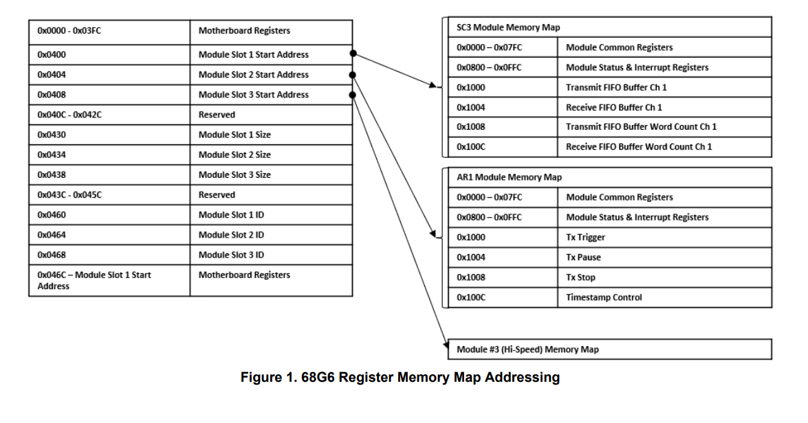
Motherboard Registers:
Read/Write access to the motherboard registers starts with the base address for the board and then the motherboard base offset address.
For example, to address Module Slot 1 Start Address register (i.e. register address = 0x0400):
- Start with the base address for the board.
- Add the motherbase register address offset.
| Motherboard Address = | Base Address Motherboard Address Offset | = 0x0000 0400 |
| 0x0000 0000 + 0x0400 |
Module Registers:
Read/Write access to the Function module’s registers start with the base address of the board. Add the “content” for the Module Start Address and then, add the specific module function register offset.
For example, to address an appropriate/specific function module with a register offset:
- Start with the base address for the board.
- Add the value (contents) from the module base address offset register (contents/value of Motherboard Memory register for Module 1 (i.e., @ 0x0400) = 0x4000.
- Then add the specific module function Register Offset of interest (i.e., A/D Reading Ch 1 @ 0x1000)
| (Function Specific) Address = | Base Address + | Module Base Address Offset + | Function Register Offset | = 0x0000 5000 |
| 0x0000 0000 | 0x4000 | 0x1000 |