
Overview
Purpose: NAI’s documentation has everything you need to bring up a multi-board VPX system, but it is spread across manuals, data sheets and guides, and the right reading order isn’t obvious. This page stitches those documents into a single, ordered path from an unopened development chassis to a running application, using one concrete example so you can see exactly which document to open at each step.
You have an NAI development chassis holding a 68INT6 Intel single-board computer that carries an EM2 dual-port Ethernet module and a DF2 discrete I/O module, plus a 68G5P multifunction I/O board beside it with more modules. You want to go from the shipping box to a running application: one that opens the 68G5P over the backplane, drives a DF2 channel, reads it back on a second channel, and prints the result.
The instructions for each step already exist across NAI’s documentation. What’s easy to miss is the order, which document owns which step, and how you know each step actually worked before you move to the next. This page is that map. Because a VPX system arrives as a box of boards, rear transition modules, adapters and cables, the connect stage is the longest one here; the software stages are shorter than on an ARM board, because the 68INT6 is its own development machine.
This user story follows one specific, internally consistent path:
68INT6 (Ubuntu) → Linux x86 Software Support Kit (SSK 2.x) built on the board →
naipcidriver → 68G5P over backplane PCIe → run from the board’s own terminal.
The parts list is modeled on a typical NAI development kit. Yours may differ in slot count, module mix or accessory quantities, and your packing list is the authority. If your slave board is a 68G5 rather than a 68G5P, or your 68INT6 came with the older 68RTINT6-1 rear module, the differences are called out in the Variants note in stage 3.
Other user stories: 68ARM2 + AD module (PetaLinux, cross-compile).
The journey at a glance
The Tool column names what you need at each stage; each stage links to the document that owns the detail. The stages are written out below the table.
| # | Stage | Tool | Where the details live |
|---|---|---|---|
| 1 | Explore in software | ESP 2.0 | Embedded Soft Panel 2 Quick Start |
| 2 | Pick your SSK package | — | Choosing the Right SSK |
| 3 | Assemble and connect the chassis | the kit’s cables and a screwdriver | this page, 68RT-SOSA-DEBUG Data Sheet, Connectors and Cabling Info |
| 4 | Set up the dev environment on the board | Ubuntu terminal, CMake, GCC | NAI SSK CMake Build Guide for Linux |
| 5 | Read the hardware docs | ESP 2.0 | 68INT6 Manual, 68G5P Manual, DF Module Guide, DF2 Manual |
| 6 | Build a sample project | CMake | NAI SSK CMake Build Guide for Linux |
| 7 | Write your DF2 application | CMake and your editor | DF Module Guide, Opening a Software Handle to Your Board |
| 8 | Run | the board’s terminal | Running Applications from the Target |
1. Explore in software first (ESP 2.0)
Before the chassis is even unpacked you can already see what a DF2 does, and ESP is how. The Embedded Soft Panel 2 is a GUI that connects to NAI hardware and lets you read and write registers, configure channels and operate modules without writing anything. Its best feature for a newcomer is that it runs against demo sessions, so you can open a discrete I/O module with no board in front of you and nothing to break.
Download ESP from the Downloads page (it’s a separate download from the SSK) and launch it on your PC. You’ll open on a Home Menu; choose New Configuration (Simple) and a Simple Configuration Menu tab appears. Pick one board, then the board type, then a demo connection. Open a DF module, set one channel’s direction to output and change its state, set another to input, and watch the panel update. Then open the API Logger: every action you just took is written out as the underlying API call in a .txt log. The configuration you clicked through is now shown to you as code, the same naibrd_DIF_* calls you’ll recognize when you reach stage 7. The full walkthrough, with a screenshot of each screen, is the Embedded Soft Panel 2 Quick Start Guide.
ESP 2.0 also ships as a native Linux build. Once the chassis is up in stage 3 you can run it on the 68INT6 itself against the real modules; Connecting to Boards notes how.
You’re on track when: ESP is open, you’ve reached a DF module through a demo session, changed a channel’s direction and state and seen the panel respond, and spotted your actions recorded in the API Logger.
2. Pick your SSK package
ESP showed you the module; now you need the software kit that lets your own program talk to it. NAI ships the Software Support Kit (SSK) in two generations, 1.x and 2.x, each in several OS-specific packages, so “download the SSK” is really a short decision. Choosing the Right SSK has an interactive picker that asks what board you have, what OS it runs and where your application runs, and names the exact package plus its download link.
For this journey the answer is fixed, and it’s worth seeing why: a 68INT6 runs Ubuntu on the board, and your application will run on that same board, so the picker resolves to the Linux x86 Software Support Kit (SSK 2.x). (The similarly named Linux Library SSK is the 1.x CentOS package for older Intel boards; that’s the one to avoid.) The 68INT6 is the master in this chassis, and the SSK is always chosen for the master, never for the slave boards.
Download it from the Downloads page. You won’t unpack it on your PC; it goes onto the board in stage 4. Skim the NAI SSK 2.x Package Guide and the Package Layout (Linux) section of the CMake Build Guide now, so that when stage 4 says “build the drivers under linux_drivers/”, you already know where that is.
You’re on track when: you’ve downloaded a package named Linux x86 Software Support Kit (SSK 2.x) and can name its main folders (the drivers, the libraries, the board-support package, the sample source) from the package guide.
3. Assemble and connect the chassis
Everything from here on happens on the 68INT6, so this stage ends with the board booted to its Ubuntu desktop and every module signal you need reachable at a jack or a screw terminal. It’s the longest stage because a VPX development system is delivered as parts: the chassis, the boards, one rear transition module (RTM) per board, and a bag of adapters and cables. Work through it in order with the chassis power off until the last step. Connector part numbers and cable options for every NAI product are collected in Connectors and Cabling Info.
What arrived
Lay the kit out and identify each piece against this table before you plug anything in. Quantities are for one 68INT6 and one 68G5P; a kit for a chassis with more boards simply repeats the per-board rows.
| Item (NAI P/N) | Qty | What it’s for |
|---|---|---|
| Development chassis (ELMA Type 32 portable tower, 6 or 8 slots, air-cooled) | 1 | Backplane, power supply and fans. Front slots take the boards; the rear slots behind them take the RTMs. |
| 68INT6-N-… | 1 | The Intel SBC. The -N in the part number is the NAI-XMC option that gives it two module slots; here slot 1 holds the EM2 and slot 2 the DF2. |
| 68G5P-2-… | 1 | The slave I/O board, three module slots. In this story slot 1 holds a DF2. |
| 68RT-SOSA-DEBUG | 1 | RTM for the 68INT6: RJ45, DB9 console, mini DisplayPort, USB, SATA, and two inboard 44-pin module headers, J5 and J7. |
| 68RTG5P-1 | 1 | RTM for the 68G5P: two 50-pin module connectors and a mini-HDMI utility jack. |
| 68RTINT6-ETH-ADPT-A-B003 | 1 | The Ethernet adapter: a small board with one 44-pin header and three RJ45 jacks. It turns the EM2’s module I/O into ordinary Ethernet ports. |
| 250-223-1 | 1 | 5-inch, 44-pin ribbon cable between RTM J5 and the adapter. |
| CBL-KIT-44 | 1 | A 44-pin one-to-one cable plus a 44PIN-DEVELOPMENT-BD screw-terminal board, for the DF2 on RTM J7. |
| 250-210-1 | 1 | 68G5P breakout cable: two 50-pin plugs for the 68G5P RTM, fanning out to two 44-pin plugs (module slots 1 and 2) and three RJ45 jacks (module slot 3). |
| 44PIN-DEVELOPMENT-BD | 2 | Screw-terminal boards for the two 44-pin plugs above. |
| 75SBC4-BB | 1 | Mini-HDMI breakout to DB9 serial and RJ45, for the 68G5P RTM’s utility jack. |
| Mini DisplayPort to DisplayPort adapter; USB-to-DB9 serial adapter; SATA data and SATA power cables | 1 each | Video, optional console and optional drive on the 68INT6 RTM. |
Seat the boards and their RTMs
NAI normally ships the boards installed, but check every one, and use the same technique for any board you add later.
- Power off. None of these boards is hot-swappable; never insert or remove one with the chassis powered.
- Front slots. The 68INT6 and the 68G5P each go in the slot named on your configuration sheet. Start with the injector/ejector handles angled open and slide the board in until the handle teeth reach the slots in the chassis frame. Rotate both handles toward horizontal; the teeth lever the board the last fraction of an inch into the backplane connectors, and the handles lock flat when it’s fully seated. To remove a board, release the handles and rotate them open; they lever the board out the same way.
- Rear slots. Each RTM goes in the rear slot directly behind its board (the rear slot numbers mirror the front). Seat it with the same handle technique. The 68RT-SOSA-DEBUG is longer than a standard RTM and its data sheet notes it has no standard securing in a commercial chassis, so make sure it is fully engaged and not resting on its backplane connector alone.
- Blanking panels go on every empty front slot so the fans pull air through the boards rather than around them.
- Leave the chassis power cord for last.
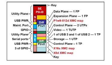 The 68INT6’s rear P0, P1 and P2 connectors and what each carries; these are what mate to the RTM through the backplane.
Cable the 68INT6’s RTM
All of the 68INT6’s own I/O comes out of the 68RT-SOSA-DEBUG’s panel and inboard headers. The RTM data sheet has the layout drawing that labels every connector; the photo below is the board’s top side.
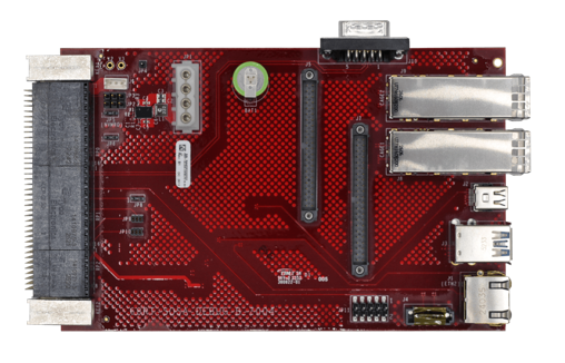
| RTM connector | Carries | Connect | Needed for this story? |
|---|---|---|---|
| J1 RJ45 | the 68INT6’s own Gigabit port (Intel I226) | Cat5e/Cat6 to your lab network | yes, this is how the board reaches the internet and how you reach it over SSH |
| J2 mini DisplayPort | video | the mini-DP-to-DP adapter, then a DisplayPort monitor | yes, the Ubuntu desktop appears here |
| J3 stacked USB 3.0 | keyboard, mouse | yes | |
| J10 DB9 | RS-232 console | the USB-to-DB9 adapter to your PC; 115200 baud, 8 data bits, no parity, 1 stop bit, no flow control | optional, useful for watching the BIOS power-on self-test |
| J4 + JP1 | SATA data + power | the SATA cables to a 2.5-inch drive | optional |
| J5 44-pin header | module slot 1 = EM2 | the ribbon cable and Ethernet adapter, see the fold-out below | yes |
| J7 44-pin header | module slot 2 = DF2 | the 44-pin cable and dev board, see “Break out the DF2” below | yes |
| J8, J9 SFP+ | 10GbE KX | no | |
| JP4 to JP11 | jumpers and sockets | leave at factory settings | no |
Cabling the EM2 (or EM1) Ethernet adapter
Why there’s an adapter at all. A module in slot 1 sends its I/O to the backplane as 44 generic pins, and the RTM brings those pins to header J5 unchanged. For an A/D module those pins would go to a screw-terminal board. For an Ethernet module they need RJ45 jacks, and that is the adapter’s only job: it puts the EM2’s two ports on standard sockets. Three parts are involved: RTM header J5, the 250-223-1 ribbon cable, and the 68RTINT6-ETH-ADPT-A-B003 adapter board.
Steps, with the chassis still off:
- Find the 44-pin header labeled J5 on the RTM’s board (the data sheet’s layout drawing labels it; J7 is its twin for module slot 2). The J5 drawing on the data sheet shows which end is pin 1.
- Plug one end of the ribbon cable onto J5 with the red stripe at pin 1. The two ends of the cable are identical sockets; either end can go on the RTM.
- Plug the other end onto the adapter’s 44-pin header J1, again red stripe to pin 1 (marked “1” beside a square pad on the adapter silkscreen).
- The kit provides no bracket for the adapter; it rides on the 5-inch ribbon behind the RTM. Route it so it clears the neighboring RTM’s handle and faceplate, support it rather than letting it hang on the header, and confirm both RTMs still seat fully.
- Run Cat5e/Cat6 from jack J2 (labeled ETH1) and jack J3 (ETH2) to your switch or PC. Jack J4 (ETH3) stays empty: the adapter is built with three jacks so that a future three-port module can use the same parts.
Which pins carry what. Each Ethernet port is four twisted pairs, TP0 to TP3. The EM2 puts them on the module’s generic I/O lines, the RTM puts those lines on J5, and the adapter routes them to a jack. The mapping below is assembled from the pin-out appendix of the EM2 Manual (module signal to I/O line) and the J5 table on the RTM data sheet (I/O line to header pin). You never wire these yourself; the table is here so you can trace a fault.
EM2 port Adapter jack RTM J5 pins (TP0+/−, TP1+/−, TP2+/−, TP3+/−) Port 1 ( ETH1)J2 “ETH1” 8/30, 10/32, 12/34, 13/35 Port 2 ( ETH2)J3 “ETH2” 2/24, 3/25, 5/27, 7/29 An EM1 has the same pin assignment, so an EM1 cables identically. Jack J4 is wired to the module’s remaining I/O lines, which a two-port module leaves unused, so it stays dark.
You’re on track when (after the board boots in the last step of this stage):
ip linkon the 68INT6 lists two more interfaces than the board has without the module,lspci | grep -i ethernetshows the onboard I226 plus two Intel E610 functions, and the link LED on each adapter jack lights when its cable goes to a live switch. Configuring the ports is ordinary Linux networking; the EM Module Guide walks through it and explains why no NAI software is involved.
Break out the DF2 on J7
The 68INT6’s second module slot comes out on header J7, the twin of J5, and because the DF2 is a discrete I/O module its pins go to screw terminals rather than jacks. Plug the CBL-KIT-44’s 44-pin cable onto J7 (match pin 1 as you did on J5) and its other end onto the 44PIN-DEVELOPMENT-BD. The dev board fans the 44 pins out to numbered screw terminals, so every module signal is a screwdriver away.
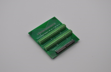
The DF2’s channels are differential pairs, and the pin-out appendix of the DF2 Manual (44-pin column) puts channel 1 on terminals 2 (IOHI-CH01) and 24 (IOLO-CH01) and channel 2 on 3 and 25. This is the 68INT6’s own DF2, the one you can exercise from ESP in stage 5. The application you write in stage 7 drives the DF2 on the 68G5P instead, so the loopback jumper goes on that board’s dev board, in the next section.
Cable the 68G5P
The 68G5P’s RTM is the 68RTG5P-1. Its two 50-pin panel connectors carry all three module slots, and the 250-210-1 breakout cable plugs into both of them at once: tighten the jack screws on plugs P1 and P2, then land the cable’s 44-pin plug P3 (module slot 1, the DF2) and P4 (module slot 2) each on a 44PIN-DEVELOPMENT-BD, and take the three RJ45 leads (module slot 3) to your switch if that slot holds an Ethernet module. The jack labels on this cable are slot-3 port positions, not the module’s own port numbers, so if slot 3 holds an EM2, identify which jack is which interface from Ubuntu with ethtool -p rather than trusting the label.
The P3 dev board is where the stage 7 application does its work. Its terminals follow the same 44-pin layout as the DF2 Manual’s 44-pin column, so the 68G5P’s DF2 has channel 1 on terminals 2 and 24 and channel 2 on 3 and 25. Run one jumper wire from terminal 2 to 3 and another from 24 to 25: that loops channel 1 into channel 2, so the application can drive one channel and read the other back with no external equipment.
The 68G5P’s console comes out on the RTM’s mini-HDMI jack JP3, together with Ethernet port 1 when the part number redirects that port to the rear I/O (by default port 1 is on the 68G5P’s own front mini-HDMI, J5). Plug the 75SBC4-BB breakout into JP3: the breakout’s DB9 is the 68G5P console (same 115200 8-N-1 settings) and its RJ45 carries Ethernet port 1 only if it is rear-routed. You won’t need either for this story, because the 68INT6 talks to the 68G5P over the backplane, but they are how you would watch the slave boot or reach it directly.
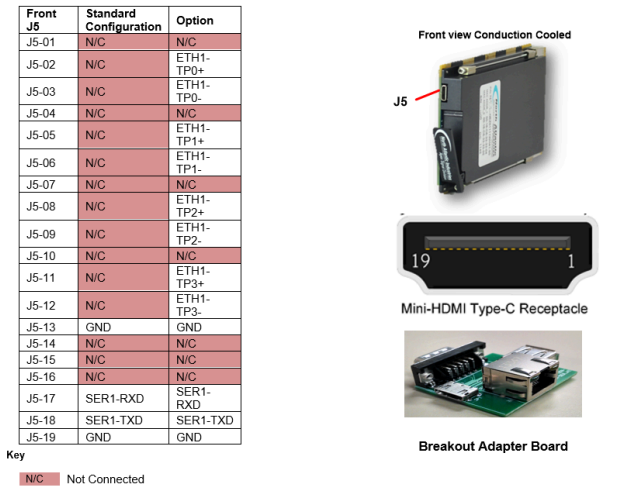 The 68G5P’s own mini-HDMI utility connector J5, its pin map, and the breakout adapter board. In a chassis the RTM’s JP3 carries the same console signals to the rear.
The 68G5P Manual has the module-slot addressing and the P1/P2 pin tables; the 68RTG5 Data Sheet is the closest published RTM reference for this family.
Variants
- 68G5 instead of 68G5P. The 68G5 is controlled the same way, over backplane PCIe from the 68INT6 (or over Gig-E), so stages 4 to 8 are unchanged. What differs is the hardware around it: its RTM is the 68RTG5-2, its module I/O breaks out through the CBL-KIT-50-3 (50-to-44 adapter cable plus dev boards) instead of the 250-210-1, and it lacks the 68G5P’s external PCIe and SATA module interfaces, so it cannot carry an EM2 in slot 3.
- Two SBCs in one chassis. Each 68INT6 gets its own RTM, adapter, ribbon and cable set, and which slave boards each SBC sees over PCIe is fixed by the backplane and your configuration sheet; the story below is the same for each SBC.
- Older 68RTINT6-1 RTM. It has a mini-HDMI jack (JP19) in place of the RJ45 and DB9; a 75SBC4-BB breakout on that jack gives you the same console and Ethernet port. Its J5/J7 headers and the Ethernet-adapter steps are identical.
Power up
Connect the chassis power cord and switch it on. Fans spin up, the 68INT6’s front LEDs go green (blinking while it initializes, steady when ready), the BIOS power-on self-test runs, and Ubuntu boots to a desktop on the monitor. The factory login is user nai, password 123456 (see the 68INT6 Manual); change it once you’re in.
You’re on track when: every board and RTM is seated with its handles locked, the 68INT6’s LEDs are steady green, the Ubuntu desktop is on your monitor, ip link in a terminal shows the board’s own port plus the EM2’s two, and the link LEDs on the adapter jacks light when cabled to a live switch. You’ll confirm the 68G5P is visible over PCIe in stage 4, after the driver is loaded.
4. Set up the development environment on the board
On an ARM board you would now install a cross-compiler on your PC. On the 68INT6 there is nothing to cross-compile: the board runs a full Ubuntu desktop, so the SSK is built and run right there, and the “development environment” is a terminal on the board. Connecting to Boards describes this onboard flow and how it differs from the cross-compile one.
Get the SSK onto the board. Copy the Linux x86 SSK 2.x package you downloaded in stage 2 onto the 68INT6 (USB stick, or scp over the J1 port now that the board has an address) and unzip it under your home directory.
Build and load the two NAI drivers. This is the step that makes the 68G5P reachable. The CMake Build Guide explains both: naipci carries PCIe traffic between the 68INT6 and any NAI board on the VPX backplane, and naigspi talks to the 68INT6’s own onboard peripherals. Follow its NAI Linux Drivers section (CMake 3.22.1 or later first, then make in each driver folder, then the install target and modprobe). The confirmation is one command:
$ lsmod | grep nai
naipci                 ...
naigspi                ...
Both names listed means the kernel is ready to hand NAI hardware to the SSK.
See the slave on the bus. NAI’s PCI vendor ID is 0x15AC (see the Glossary), so:
$ lspci -d 15ac:
lists every NAI PCIe device the 68INT6 can see. Expect one line for the 68INT6’s own NAI-XMC module carrier (the -N option) and one more for the 68G5P; the 68G5P’s line is the one with device ID 6881 (from the 68G5P Manual), so lspci -d 15ac:6881 singles it out. If that second line is missing, the 68G5P is not seated or the backplane routes it to a different SBC; go back to stage 3 before continuing.
You’re on track when: the SSK is unzipped on the board, lsmod shows naipci and naigspi, and lspci -d 15ac:6881 shows the 68G5P.
5. Explore modules and read the hardware docs
With the drivers loaded, take a short detour back to the hardware, because the code you write next has to match the exact modules in your chassis. Run the native Linux build of ESP 2.0 on the 68INT6 (stage 1 pointed to it) and look at the modules it reports: the DF2 in the 68INT6’s slot 2 and, with the master/slave configuration set up, the modules on the 68G5P as well. The EM2 will not appear as a module here, because it isn’t one to the SSK; it’s a network card owned by Ubuntu, which is the point made in the EM Module Guide.
Then confirm the details in the documentation. The DF Module Guide opens with an at-a-glance table of the family: a DF2 is 16 channels of programmable differential I/O with per-channel PWM, pattern generation and pulse-timing measurement on top of plain input/output, while a DF1 is the plain version, and both use the same naibrd_DIF_* API. The DF2 Manual gives every register, and its pin-out appendix is where the terminal numbers you jumpered in stage 3 came from. The 68G5P Manual covers module-slot addressing on the slave, and the 68INT6 Manual covers the SBC itself, including the NAI-XMC option that gives it module slots. The RTM data sheet and the EM2 Manual round out the set; the connector tables you cabled from in stage 3 live there.
You’re on track when: ESP on the board lists the DF2 and the 68G5P’s modules, and you can say which module slot the DF2 occupies on each board and which two terminals its channel 1 uses.
6. Build a sample project
Before writing anything of your own, build one of NAI’s sample applications from start to finish. A clean build of code you know is good proves the toolchain, the SSK and the drivers all line up, so if your own build later fails you can trust the problem is your change.
Follow Building and Running a Project in the CMake Build Guide: configure with the default linux_x86-64.cmake toolchain, build, and watch the output folder fill with executables. Pick the Board Access sample (Board Access) as the one you’ll run first, because it exercises nothing but the connection workflow, opening the boards and reporting what it finds, which is exactly the check you want.
You’re on track when: the build finishes with no errors and a board_access executable sits in the build output.
7. Write your DF2 application
Now build the thing you set out to make: an app that opens the 68G5P, sets DF2 channel 1 to output and channel 2 to input, drives channel 1 high and low, reads channel 2 back through the jumper you fitted in stage 3, and prints both states. Don’t start from an empty file. Copy DIF BasicOps, the SSK’s DIF sample, and work subtractively: it already opens the board, finds the modules and configures channels, so you keep the parts you need and delete the rest. Read DIF BasicOps first; it walks the code section by section and is written in the current 2.x style, so treat it as your model whenever another example looks different.
Two pieces sit at the heart of the app.
Opening the slave over the backplane. Opening a Software Handle to Your Board has a section for exactly this configuration, NAI Processor access via Native PCI/cPCI/PCIe Bus: you open the 68INT6 itself with NAIBRD_COMM_ONBOARD, then for the slave call naibrd_SetBusDev with lane 1 (lane 0 is the NAI processor board, lane 1 is any slave) and the bus, device and function from the 68G5P’s lspci line in stage 4, then naibrd_OpenDevice with NAIBRD_COMM_PCI and the board’s name constant from naibrd.h (the pattern is NAI_DEV_NAME_<board>; spotting the 68G5P’s entry there is your sign you’ve found the right hook).
Driving and reading the DF2. The DF Module Guide’s Try it — Drive an output and read an input snippet is the whole sequence, in SSK 2.x form:
naibrd_DIF_SetIOFormat(cardIndex, module, chOut, NAIBRD_DIF_GEN5_IOFORMAT_OUTPUT);
naibrd_DIF_SetIOFormat(cardIndex, module, chIn,  NAIBRD_DIF_IOFORMAT_INPUT);

naibrd_DIF_SetOutputState(cardIndex, module, chOut, NAIBRD_DIF_STATE_HI);

naibrd_dif_state_t state;
naibrd_DIF_GetInputState(cardIndex, module, chIn, &state);
Use channel 1 for chOut and channel 2 for chIn, matching the jumper (check whether your sample counts channels from 0 or 1 at its channel prompt). Drive HI, read, drive LO, read, and print both readings.
Because “writing code” doesn’t produce a screen you can match against a picture, your confirmation is the same one as stage 6: the project builds cleanly to an executable.
You’re on track when: your application compiles, and you can point to the line that opens the 68G5P over PCI, the line that sets channel 1’s direction, and the line that reads channel 2.
8. Run on the target
This is the payoff, and it’s quick because the executable is already on the machine that will run it. From the board’s terminal, cd to the build output and launch it:
$ ./your_app
NAI sample-derived apps open with a short configuration menu asking what kind of system you have, where the app is running and how it reaches the modules. Your app runs on the master SBC and reaches a slave over the backplane, which is scenario D, Onboard master, backplane slaves in Running Applications from the Target: at the system prompt type B for board and give the number of NAI boards in the chassis (or S if the SIU list names your chassis), answer 2 (local NAI processor card) for where the app runs, and pick the master board type. The app enumerates the 68G5P over PCI, prints its modules and offers to save the configuration so you can skip the prompts next time. Then your own code takes over.
You’re on track — and done — when: the app prints the 68G5P’s modules, then prints channel 2 reading HI while channel 1 is driven high and LO while it’s driven low. Those two readings are the whole journey paying off: your code, on your board, driving a real signal across a real wire and reading it back.
Related
- User Story: 68ARM2 + AD Module — the same journey on an ARM board with a cross-compile flow
- Embedded Soft Panel 2 Quick Start — code-free exploration (Stages 1, 5)
- Choosing the Right SSK — package selection (Stage 2)
- 68RT-SOSA-DEBUG Data Sheet · Connectors and Cabling Info — RTM connectors, cables and breakout boards (Stage 3)
- EM Module Guide · EM2 Manual — the Ethernet module and its pins (Stage 3)
- Connecting to Boards — the onboard Linux x86 flow (Stage 4)
- NAI SSK CMake Build Guide for Linux — drivers and build (Stages 4, 6)
- 68INT6 Manual · 68G5P Manual · DF Module Guide · DF2 Manual — hardware reference (Stage 5)
- Opening a Software Handle to Your Board · Board Access · DIF BasicOps — code scaffolds (Stage 7)
- Running Applications from the Target — the run-time menu (Stage 8)