DATA SHEET
Click here for the 68INT6 data sheet
INTRODUCTION
North Atlantic Industries (NAI) is a leading independent supplier of rugged COTS embedded computing products for industrial, commercial aerospace, and defense markets. Aligned with MOSA, SOSA and FACE standards, NAI’s Configurable Open System Architecture™ (COSA®) accelerates a customer’s time-to-mission by providing the most modular, agile, and rugged COTS portfolio of embedded smart modules, I/O boards, Single Board Computers (SBCs), Power Supplies and Ruggedized Systems of its kind. COSA products are pre-engineered to work together, enabling easy changes, reuses, or repurposing down the road. By utilizing FPGAs and SoCs, NAI has created smart modules that enable the rapid creation of configurable mission systems while reducing or eliminating SBC overhead.
NAI’s 68INT6 3U OpenVPX SOSA™-Aligned Intel® Single Board Computer supports a wide range of input and output capabilities, including analog and digital I/O, signal generation and acquisition, and communication interfaces. When combined with these smart modules, the board’s modular I/O approach makes it a highly flexible and integrable solution for demanding computing environments
68INT6 Overview
The 68INT6 3U OpenVPX SOSA™-Aligned Intel® Single Board Computer offers a variety of features designed to meet the needs of complex requirements for integrated multifunction I/O-intensive, mission-critical applications. Some of the key features include:
3U Profiles supported: This board is aligned with Sensor Open Systems Architecture (SOSA) and VITA 65 OpenVPX Profile standards, with module and slot profiles specified as:
- MOD3-PAY-1F1F2U1TU1T1U1T-16.2.15-2
- SLT3-PAY-1F1F2U1TU1T1U1T-14.2.16
The SOSA-aligned and OpenVPX Profile(s) compatibility ensure interoperability with other components and promote system-level integration for efficient optimized performance.
PCIe connectivity: The 68INT6 provides highly flexible and efficient high-speed connectivity between the 68INT6 board and host SBCs data/expansion planes (routed on the VPX (P1) connector):
-
One x4 or four x1 PCIe (Gen 3) on the data plane:
- The x4 configuration enables high-speed data transfer on a single PCIe slot due to the four lanes.
- The x1 configuration allows for connection to multiple devices/expansion cards with lower individual bandwidth due to having 4 PCIe slots with one lane each.
-
Four x1 or one x4 PCIe (Gen 3) on the expansion plane:
- The x1 configuration is suitable for accommodating multiple expansion cards with lower bandwidth requirements.
- The x4 configuration is ideal for connecting a single expansion card that requires higher bandwidth.
-
8 x1 PCIe (Gen 3) combined planes:
- By default, the data and expansion planes are used together, providing eight total PCIe slots with one lane each. This configuration provides a balance between the number of slots and individual bandwidth, giving the 68INT6 application versatility.
Intel® Tiger Lake i7-118xGRE Certifiable Processor with integrated PCH-LP: The 68INT6 is powered by the latest Intel® Tiger Lake i7-118xGRE certifiable processor which provides several benefits for applications in rugged environments such as military, aerospace, and industrial sectors:
-
With four processing cores, the i7-118xGRE certifiable processor is well-suited for compute-intensive tasks. In the case of an SBC, this means the ability to handle complex data processing, real-time control, and mission-critical calculations efficiently.
- There is also support for multithreading, enabling the processor to handle multiple tasks simultaneously. In applications like radar signal processing, image analysis, or communication systems, this ensures optimal utilization of the CPU, enhancing overall system performance.
-
The processor’s 12MB Smart Cache helps reduce memory access latency, which is especially beneficial to data-intensive applications like sensor data fusion, where quick access to large datasets is crucial for real-time decision making.
-
With a maximum clock speed of 2.8 GHz, the processor provides crucial computational speed benefits to time-sensitive tasks. In military applications, such as unmanned systems or command & control systems, this speed ensures timely response to changing scenarios.
-
The integrated PCH-LP (Platform Controller Hub - Low Power) enhances energy efficiency. In applications where power constraints are common (e.g. in the field), an energy-efficient SBC helps extend mission durations on battery power, or reduce the load on power supplies in constrained environments.
- In addition, the PCH-LP includes various interface and connectivity options such as USB, PCIe, SATA and Ethernet. This versatility enables the 68INT6 to connect with a wide range of peripherals and external devices, making it adaptable to different applications.
Note
The 68INT6 can be built and delivered with two processor versions; the i7-1185GRE (standard) and i7-1186GRE (certifiable). Both versions of the processor feature the same characteristics, with the exception that the i7-1186GRE is considered ‘certifiable’ as it includes an Intel factory configuration that disables automatic power/thermal throttling. This factory configuration enables the i7-1186GRE to be used in safety-critical environments (thought it should also be noted that actual safety certification would be dependent on the specific application, requirements, and standards that need to be met at the higher-level integrated system).
Up to 64 GB DDR4 SDRAM (2 banks) w/In-Band ECC memory: The SBC features up to a 64 GB DDR4 SDRAM, which offers users a powerful memory solution for demanding military, industrial, and aerospace environments:
- The large memory capacity allows the 68INT6 to handle extensive data sets, complex computations, and multitasking efficiently.
- The DDR4 SDRAM improves performance and energy efficiency by way of its high data transfer rate and low power consumption.
- The two banks configuration offers flexibility in memory allocation and management.
- With in-band ECC, the SDRAM utilizes the same memory space for stored data and ECC bits, in addition to featuring immediate error correction, which ensures only correct data is delivered to the processor or application.
Up to 512 GB SATA III SSD: The 68INT6 utilizes a SATA III Solid State Drive (SSD) capable of providing up to 512 GB of storage, offering high-capacity, high-speed, reliable, and energy-efficient data storage. It addresses the unique needs of military, industrial, and aerospace environments by ensuring data integrity, durability, and rapid access to critical information.
Backup-boot NOR FLASH BIOS: The inclusion of backup-boot NOR FLASH BIOS memory enhances system reliability, data integrity, and security in military, industrial, and aerospace environments. It provides a failsafe mechanism for BIOS recovery, ensuring critical systems remain operational even during unforeseen failures or disruptions, providing crucial redundancy/reliability in applications where system downtime can have severe consequences.
Video: The 68INT6 can output video signals through a DisplayPort interface with exceptional capabilities. It can handle extremely high resolutions of up to 7680 x 4320 at a smooth 60 Hz refresh rate, making it suitable for:
- Military applications - allows for detailed and high-quality video feeds for situation awareness, surveillance and targeting. Having access to clear, detailed visuals enhances decision-making and threat detection capabilities.
- Industrial settings - provides precision monitoring and control of complex machinery via precise, high-resolution video. High resolution video output is valuable to industries that rely on automation and advanced control systems.
- Aerospace - enables clear and detailed visualization for navigation, monitoring, and communication systems. Used for cockpit displays, navigation maps and ground control communication, the clarity of visuals is vital for pilot decision-making and safe flight operations.
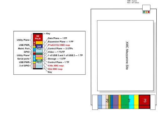
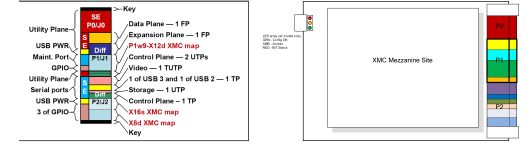
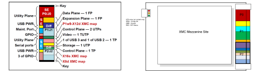
XMC functionality: Providing a perfect solution SOSA™-aligned rugged commercial, industrial, and aerospace applications, the 68INT6 supports XMC 1.0 (VITA 42) or XMC 2.0 (VITA 61). This offers a versatile platform for adding additional processing power, I/O capabilities, and/or specialized functionalities to the board. In addition, the optional NAI XMC module provides the capabilities of other NAI SBCs by way of NAI’s family of COSA® smart function modules.
1x 10/100/1000 Base-T and 2x 10GBase-KR Ethernet: The 68INT6 provides 10/100/1000 Base-T and 10GBase-KR Ethernet ports to the rear of the board. These ports provide data communication capabilities and network connectivity for advanced control and data acquisition applications.
IPMC support (option): The 68INT6 board has IPMC (Intelligent Platform Management Controller) support, which is VITA 46.11 Tier-2 compatible. This allows for advanced system monitoring and control from the host Chassis Manager.
Advanced security options: The board offers advanced security options, including up to FIPS 140-3 Layer 3 Hardware Support for secure boot and tamper detect. Contact NAI with security requirements to determine appropriate enhanced security function implementation.
Support for two independent, smart function modules (NAI-XMC option): When configured with NAI’s XMC module, the board can support up to two independent, smart function modules based on the COSA® architecture. With over 100 modules to choose from, this allows for a wide range of input and output capabilities, including analog and digital I/O, signal generation and acquisition, and communication interfaces. Each function module slot on the NAI XMC has an independent x1 SerDes interface for motherboard-to-smart module interface, to offload the host processor from I/O management.
- The 68INT6’s function slot #1 features a PCIe interface that enables up to 2 additional Gig-E ports while function slot #2 boasts an independent external SATA II interface that supports memory expansion over the VPX backplane. These interfaces facilitate the expansion of external host SBC functions, which enables engineers and system architects to easily configure the board with the necessary modules and accelerate SWaP-optimized system deployment.
Peripheral I/O: The 68INT6 board features several sophisticated on-board (on motherboard) peripheral I/O interfaces, all of which are rear accessed. Designed to meet the diverse requirements of complex projects, this comprehensive I/O suite includes:
-
A high-speed USB 3.x interface, which provides fast data transfer rates which facilitates efficient communication with peripheral devices such as storage drives, sensors, and actuators, enabling users to transfer large amounts of data quickly and reliably.
-
Four TTL general-purpose input/output (GPIO) pins that provide versatile connectivity options for sensors, actuators, and other digital electronics, allowing for the creation of custom control systems and embedded applications tailored to specific project requirements.
-
One RS422/485 or two RS-232 ports, configurable via a programmable serial transceiver. This allows for robust serial protocol support on a single 3V-5.5V supply.
-
An RS-232 console/maintenance port that provides a standard interface for communicating with the board for maintenance and debugging purposes. This serial port can be used for configuring the board or accessing diagnostic information and logs.
Background Built-In-Test (BIT): The 68INT6 board supports function module BIT, which continually checks and reports on the health of each channel, allowing for proactive maintenance and reducing the likelihood of downtime.
Software Support Kits (SSKs): SSKs are provided ‘free of charge’ and include base motherboard and function module API libraries and documentation. Sample and source code are also available, as well as support for real-time operating systems (RTOS) such as Windows, DDC-I Deos, Wind River Linux and HVP, Ubuntu 22.x Linux, Lynx MOSA.ic, and Green Hills Integrity-178 tuMP (contact factory), providing developers with flexibility and customization options for their specific application needs.
Commercial and rugged mechanical options: The 68INT6 is available in both commercial and rugged models, making it suitable for a wide range of applications.
- Operating temperature:
The board has a wide operating temperature range, with models operating from:
- 0° C to 55° C (commercial model)
- -40° C to +85° C (rugged model)
Power: The 68INT6 has a simple and efficient inboard power management system, requiring only a +12V (VS1) and +3.3V_AUX supply to power the main and auxiliary components, respectively, while consuming up to 55W estimated typical power, depending on the board’s configuration (number of cores, core speed, DDR speed, OS, application, etc).
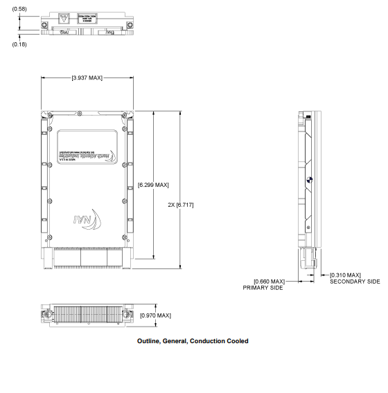
Mechanical design: The mechanical design of the 68INT6 conforms to 3U 5HP/1.0” pitch form factor ANSI/VITA standard 48.1 (air cooled) and 48.2 (conduction cooled) and is ideal for commercial development or rugged and deployable applications.
Overall, the 68INT6 3U OpenVPX SOSA™-Aligned Intel® Single Board Computer is a reliable and versatile solution for demanding computing environments that require high-performance and flexible I/O capabilities.
SPECIFICATIONS
General for the Motherboard
| Signal Logic Level: | Supports LVDS PCIe ver. 3.0 bus (x1) |
| Power (Motherboard): | `12 VDC @ <4.6 A (est. max. typical)* ` `3.3V_AUX @ <100 mA (typical) ` *dependent on the number of cores, core speed, DDR speed, OS, application, etc. |
| Temperature, Operating: | "C" =0° C to +55° C, "H" =-40° C to +85° C (see part number) |
| Storage Temperature: | -55° C to +105° C |
| Temperature Cycling: | Each board is cycled from -40° C to +85° C for option “H” |
| General size: Height: | 3.94" / 100 mm (3U) |
| Width: | 1.0” / 25.4 mm (5 HP) air cooled front panel options |
| Depth: | 6.3“ / 160 mm deep |
| Weight: | 28 oz. (794 g) unpopulated (approx.) (air or conduction cooled) + >> then add weight for each module (typically 1.5 oz. (42 g) each) (NAI-XMC Configuration only) |
Note
Specifications are subject to change without notice.
Environmental
Unless otherwise specified, the following table outlines the general Environmental Specifications design guidelines for board level products of North Atlantic Industries. All our cPCI, VME and OpenVPX boards are designed for either air or conduction cooling. All boards also incorporate appropriate stiffening to ensure performance during shock and vibration but also to assure reliable operation (lower fatigue stresses) over the service life of the product.
| Parameters | Level | ||
| 1 / Commercial-AC (Air Cooled) | 2 / Rugged-AC (Air Cooled) | 3 / Rugged-CC (Conduction Cooled) | |
| Temperature - Operating | 0° C to 55° C, AmbientH | -40° C to 85° C, AmbientI | -40° C to 85° C, at wedge lock thermal interface |
| Temperature - Storage | -40° C to 85° C | -55° C to 105° C | -55° C to 105° C |
| Humidity - Operating | 0 to 95%, non-condensing | 0 to 95%, non-condensing | 0 to 95%, non-condensing |
| Humidity - Storage | 0 to 95%, non-condensing | 0 to 95%, non-condensing | 0 to 95%, non-condensing |
| Vibration - SineA | 2 g peak, 15 Hz - 2 kHz^B | 6 g peak, 15 Hz - 2 kHzB | 10 g peak, 15 Hz - 2 kHzC |
| Vibration - RandomD | .002 g2 /Hz, 15 Hz - 2 kHz | 0.04 g2 /Hz, 15 Hz - 2 kHz | 0.1 g2 /Hz, 15 Hz - 2 kHzE |
| ShockF | 20 g peak, half-sine, 11 ms | 30 g peak, half-sine 11 ms | 40 g peak, half-sine, 11 ms |
| Low PressureG | Up to 15,000 ft. | Up to 50,000 ft. | Up to 50,000 ft. |
Notes:
A. Based on sweep duration of ten minutes per axis on each of the three mutually perpendicular axes. B. Displacement limited to 0.10 D.A. from 15 to 44 Hz. C. Displacement limited to 0.436 D.A. from 15 to 21 Hz. D. 60 minutes per axis on each of the three mutually perpendicular axes. E. Per MIL-STD-810G, Method 5.14.6 Procedure I, Fig.514.6C-6 Category 7 tailored (11.65 Grms): 15 Hz - 2 kHz; ASD (PSD) at 0.04 g2/Hz between 15 Hz - 150 Hz, increasing @ 4 dB/octave from 0.04 g2/Hz to 0.1 g /Hz between 150 Hz - 300 Hz, 0.1 g2/Hz between 300 Hz - 1000 Hz, decreasing @ 6 dB/octave from 0.1 g2/Hz to 0.025 g2/Hz between 1000 Hz - 2000 Hz. Three hits per direction per axis (total of 18 hits). F. Three hits per direction per axis (total of 18 hits). G. For altitudes higher than 50,000 ft., contact NAI. H. High temperature operation requires 350 lfm minimum air flow across cover/heatsink (module dependent). I. High temperature operation requires 600 lfm minimum air flow across cover/heatsink (module dependent).
Specifications subject to change without notice
SOFTWARE
Built-In Test
The 68INT6 supports options for Power-On-Self-Test (POST) testing (memory, peripherals, etc.). The 68INT6, when configured with an NAI XMC, also supports function modules with NAI’s flexible, leading-edge, fully programmable and continuous background built-in-test (BIT) enabled function. BIT tests on board functions and functions contained on NAI XMC-enabled expansion modules, making it a useful field service tool.
BIOS
The 68INT6 utilizes the Insyde Unified Extensible Firmware Interface (UEFI) BIOS. The BIOS provides for low level functions required by the processor core and chipset. The BIOS also controls many configuration options. The BIOS configuration controls many details concerning the behavior of the hardware from the moment power is applied. The user’s BIOS configuration options are saved in the Serial Peripheral Interface (SPI) Flash memory. Both the BIOS and BIOS configuration data is stored in the SPI Flash device. The SPI Flash is non-volatile, and the BIOS configuration settings are saved without system or battery power. There is no battery on the 68INT6. The BIOS supports several modes for booting, including remote booting from any of the Ethernet ports.
Operating System Support
The 68INT6 hardware supports the following operating systems:
- Wind River Linux and HVP
- VxWorks and VxWorks Cert Edition
- Windows
- Ubuntu 22.x Linux
- DDC-I DEOS
- Lynx MOSA.ic
- Green Hills INTEGRITY-178 tuMP
Software Support
The ENAIBL Software Support Kit (SSK) is supplied with all system platform based board level products. This platform’s SSK contents include html format help documentation which defines board specific library functions and their respective parameter requirements. A board specific library and its source code is provided (module level ‘C’ and header files) to facilitate function implementation independent of user operating system (O/S). Portability files are provided to identify Board Support Package (BSP) dependent functions and help port code to other common system BSPs. With the use of the provided help documentation, these libraries are easily ported to any 32-bit O/S such as RTOS or Linux.
The latest version of a board specific SSK can be downloaded from our website www.naii.com in the software downloads section. A Quick-Start Software Manual is also available for download where the SSK contents are detailed, Quick-Start Instructions provided and GUI applications are described therein. For other operating system support, contact factory.
INITIAL SETUP
Backplane and Power Supply
The 68INT6 requires up to 30 Watts steady state from the power supply, with sufficient margin to accommodate any additional inrush current. The PCI power supply must be capable of 2.5 A @ 12 V rail and 100 mA @ 3.3_Aux V.
Keyboard and Mouse
Depending on how the 68INT6 was configured at the factory, a keyboard and mouse may be required to set your BIOS configuration options. A mouse and keyboard can be connected to the 68INT6 for initial system setup.
Video Monitor
Refer to the 68INT6 ordering code for the video configuration option (See Part Number Designation section in this manual). Only DisplayPort is natively supported and may be used for the initial setup. Any other interface must utilize a converter from DisplayPort (some of these also require a BIOS menu setting to be changed). Note that the Video output is configured as rear I/O.
POST
Each time the 68INT6 boots, it must pass the BIOS Power-On-Self-Test (POST), which is summarized below.
- Tests the Power Supply to ensure that it is turned on and that it releases its reset signal.
- CPU must exit the reset status mode and thereafter can execute instructions.
- UEFI Firmware is readable.
- UEFI Firmware checksum must be valid, meaning that it must be readable.
- CPU must be able to read all forms of memory such as the memory controller and memory bus.
- I/O bus / controller must be accessible. If the computer does not pass any of the above tests, the board will fail the POST.
Operating Frequency
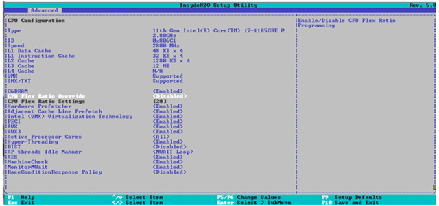
Using Intel® Speed Shift Technology*, the operating frequency will toggle from a maximum value (set in the BIOS) down to 800 MHz depending on the workload and temperature. The temperature at which the processor will start to throttle is 95°C.
*Intel® Speed Shift Technology is an energy-efficient method of frequency control by the hardware rather than relying on OS control. Processor decision is based on the different system constraints (ex. workload demand, thermal limits) while taking into consideration the minimum and maximum levels and activity window of performance requested by the Operating System.
The maximum operating frequency value can be set in the BIOS via the ‘Advanced >> CPU Configuration >> CPU Flex Ratio Setting’ menu.
-
The default setting is [28], which corresponds to a maximum value of 2.8 GHz.
-
The minimum setting is [8] which corresponds to a value of 800 MHz.
Note
‘Advanced >> CPU Configuration >> CPU Flex Ratio Override’ MUST be set to Enabled to change the ‘CPU Flex Ratio Setting’.
Operating System Login Credentials
For users operating the 68INT6 via Ubuntu, the factory default log in is as follows:
User nai
Password 123456
68INT6 ON BOARD RESOURCES
Memory
DDR4 SDRAM
The 68INT6 provides up to a total of 64 GB DDR4 memory with In-Band ECC. This memory is organized as up to two channels of eight 2Gb x 8 MT40A2G8SA or 4Gb x8 MT40A4G8NEA devices (parts may vary). The Intel® Core™ i7-118xGRE has an on chip 64-bit DDR4 memory controller. The controller has full ECC error correction support, with the ability to detect multi-bit errors and correct single-bit errors within a nibble. Intel® In-Band ECC is used. Please consult the Micron data sheet for DDR4 device specific details.
SPI Flash
The 68INT6 supports 2 x 16 MB of serial flash, which is connected through the Intel® PCH-LP interface via a jumper. The flash memory consists of two, soldered W25R256JVEIQ SPI flash devices. The flash memory is organized as 65,526 pages of 256 bytes each. Up to 256 bytes can be programmed at a time.
The flash memory is used to store the BIOS configuration setting. The flash memory has an erase capacity of 100,000 cycles per sector and typical data retention of 20 years.
SATA
The Intel® PCH-LP is directly connected to an onboard Solid-State Drive (SSD). The SSD contains a single level cell NAND Flash together with a controller in a single BGA package. This BGA packaged device is soldered directly to the printed circuit board, for reliable electrical and mechanical connection.
The SSD has an internal write protect signal HDW_WP. It is controlled by software and can be set to a default in the BIOS. The HDW_WP signal is pulled up on card by a 4.7 KΩ resistor to the internal 3.3 V supply.
The onboard SATA drive conforms to the following specifications:
-
Complies with SATA 3.1 Specification
-
ATA/ATAPI-8 and ACS-2 command compliant
-
Supports speeds: 6 Gbps (backwards compatible to1.5 Gbps (first-generation SATA), 3 Gbps (second-generation SATA and eSATA))
-
Contains high-speed descriptor-based DMA controller
-
Supports native command queuing (NCQ) up to 32 commands
-
Supports SATA Device Sleep (DevSleep) for improved power consumption
-
Supports 28-bit and 48-bit LBA (Logical Block Addressing) mode commands
The standard ordering code for the 68INT6 includes a 256GB SSD drive. Larger devices are available; please consult the factory for availability.
Peripheral I/O
Ethernet
The 68INT6 has one Intel® I226 Ethernet PHY device that supports one 10/100/1000Base-Tx Ethernet port.
The Intel® I226 features:
-
Fully integrated GbE MAC (x1) and PHY/SERDES/SGMII in any combination
-
IEEE 1588 (pre-standard) / IEEE 802.1AS and per packet time stamping
-
IEEE 802.1Qav Audio/Video Bridging (AVB) for tightly controlled media stream synch, buffering and reservation
-
Supports four Tx & Rx Queues, Virtual Machine Data queues (VMDq), and 9.5 KB Jumbo Frames
-
Detection and correction of pair swaps (MDI crossover), and pair polarity
-
MAC-side and line-side loopback
-
Auto-negotiation
The 68INT6 additionally supports two 10GBase-KR Ethernet connections using an Intel® E810 Ethernet Controller.
The Intel® E810 features:
-
Two 100 GbE ports
-
100Gb throughput performance
-
Enhanced programmable packet processing pipeline
-
Virtualization (enhanced SR-IOV support w/up to 256 Virtual Functions [VF] and backward compatibility VF driver support)
-
RDMA (iWARP and RoCEv2)
Both connections are 10GBase-KR only and are routed to the rear of the board.
I/O pin outs can be found in the Pinout Details section of this document.
USB
The 68INT6 supports one USB 3.1 (Gen 1) port on the backplane and one USB 2.0 port on the backplane. Contact factory for availability.
USB port 1 and port 2 are available at the rear of the 68INT6, on connector P2. The USB port can operate as a standalone host.
-
Compatible with USB specification, Rev. 2.0
-
Supports high-speed (480 Mbps), full-speed (12 Mbps), and low-speed (1.5 Mbps) operations
-
Supports operation as a standalone USB host controller
-
Supports USB root hub with one downstream-facing port
-
Enhanced host controller interface (EHCI)-compatible
-
One controller supports operation as a standalone USB device
-
Supports one upstream-facing port
-
Supports six programmable USB endpoints
Video
The 68INT6 uses Intel® Core™ i7-118xGRE integrated UHD Graphics P630. This provides DisplayPort output with 4K support (at 60 Hz) as well as OpenGI and DirectX support. The DisplayPort signals are routed to the rear P2 I/O connector (see pin-out table).
The maximum resolution is 60 Hz at 7680 x 4320.
I2C
I2C is a two-wire, bidirectional single ended serial bus that provides efficient method of exchanging data between a master and slave device. The 68INT6 has one device for communicating with onboard devices, as shown in the table below.
| Assignment | I2C addresses | Device |
| Onboard Devices | 0x50 | FIPS |
| 0x56 | EEPROM | |
| 0x68 | WDT |
An I2C port is also available on the backplane as a build option (see Part Number Designation section).
Note
the 68INT6 does NOT support I2C slave mode or I2C multi-master.
SPI
Serial Peripheral Interface Bus or SPI is a synchronous serial data link standard. SPI operates in full duplex mode. SPI devices communicate in master/slave mode where the master device starts a frame and sources the clock. The PCH-LP has one SPI controller. The SPI port is attached to a SLB9670XQ2. The SLB9670XQ2 is a Trusted Platform Module that is based on advanced hardware security technology.
Serial Ports
The 68INT6 has a single, asynchronous serial port. The interface uses a two-wire, TXD, RXD interface (system/power GND referenced). The SER-TXD and SER-RXD RS-232 signals are routed in parallel to P2 at the rear of the 68INT6 and to an LTC2870 on the board. The LTC2870 is a programmable transceiver that can be configured as either one RS-422/485 or two RS-232 receivers & drivers*. Additionally, there is a third serial maintenance port that is routed to P1 at the rear of the 68INT6.
Note
*For additional information on pinout details when the programmable transceiver is configured as either RS-232 or RS-422/485, please refer to the XMC/Built-In I/O – Defined Area (P2) section of this manual.
Onboard TTL
TTL I/O are available as a configuration options (see pin-outs/P/N configuration).
TTL I/O Specifications
Note
The TTL I/O signals are non-isolated. All grounds are common and are connected to a single Digital Ground and power return.
TTL Input
| Input levels: | TTL and CMOS compatible, single ended inputs |
|---|
Input levels:
| Vin L (min): | 0 V |
|---|---|
| Vin L (max): | 0.8 V |
| Vin H (min): | 2.0 V |
| Vin H (max): | 5.0 V |
TTL Output
| Output levels: | TTL/CMOS, single ended outputs |
|---|
Drive Capability:
| Vout L (min): | 0 V min @ 16 mA (sink) |
|---|---|
| Vout L (max): | 0.45 V max @ 16 mA (sink) |
| Vout H (min): | 2.1 V @ 400 uA (source) |
| Vout H (max): | 3.3 V VCC, (unloaded) |
| Rise/Fall time: | 10 ns into a 50pf load |
PRC Register Descriptions
The register descriptions provide the Register Name, Function Address Offset, Type, Read or Write information, Initialized Value, a description of the function and, in most cases, a data table.
PRC Revision
| Function: | Processor Register Controller (PRC) firmware revision |
|---|---|
| Function Address Offset(s): | 0x00 |
| Type: | binary word (16-bit) |
| Read/Write: | R |
| Initialized Value: | Value corresponding to the current revision of the board’s Processor Register Controller |
| Operational Settings: | The 16-bits are the revision of the PRC. |
| D15 | D14 | D13 | D12 | D11 | D10 | D9 | D8 | D7 | D6 | D5 | D4 | D3 | D2 | D1 | D0 |
|---|---|---|---|---|---|---|---|---|---|---|---|---|---|---|---|
| D | D | D | D | D | D | D | D | D | D | D | D | D | D | D | D |
POSM Revision
| Function: | Power Sequence Manager (POSM) firmware revision |
|---|---|
| Function Address Offset(s): | 0x04 |
| Type: | binary word (16-bit) |
| Read/Write: | R |
| Initialized Value: | Value corresponding to the current revision of the board’s Power Sequence Manager |
| Operational Settings: | The 16-bits are the revision of the POSM. |
| D15 | D14 | D13 | D12 | D11 | D10 | D9 | D8 | D7 | D6 | D5 | D4 | D3 | D2 | D1 | D0 |
|---|---|---|---|---|---|---|---|---|---|---|---|---|---|---|---|
| D | D | D | D | D | D | D | D | D | D | D | D | D | D | D | D |
Serial Port Control
| Function: | Sets the serial port control. |
|---|---|
| Function Address Offset(s): | 0x08 |
| Type: | binary word (16-bit) |
| Read/Write: | R/W |
| Initialized Value: | 0x0000 |
| Operational Settings: | Write 0 for Dual RS232; 1 for Single RS485: + Default is configured for RS232. |
| D15 | D14 | D13 | D12 | D11 | D10 | D9 | D8 | D7 | D6 | D5 | D4 | D3 | D2 | D1 | D0 |
|---|---|---|---|---|---|---|---|---|---|---|---|---|---|---|---|
| 0 | 0 | 0 | 0 | 0 | 0 | 0 | 0 | 0 | 0 | 0 | 0 | 0 | 0 | 0 | D |
SATA Miscellaneous
| Function: | Enables user to set write protect defaults to a BIOS. Also allows for setting of Dataflush and Quick Erase. |
|---|---|
| Function Address Offset(s): | 0x94 |
| Type: | binary word (16-bit) |
| Read/Write: | R/W |
| Initialized Value: | 0x0000 |
Note
There are other bits in this register such as Quick Erase and Dataflush, so read/modify writes must be used.
| D15 | D14 | D13 | D12 | D11 | D10 | D9 | D8 | D7 | D6 | D5 | D4 | D3 | D2 | D1 | D0 |
|---|---|---|---|---|---|---|---|---|---|---|---|---|---|---|---|
| 0 | 0 | 0 | 0 | 0 | 0 | 0 | 0 | 0 | 0 | 0 | 0 | D | D | D | D |
| Bit | Name | Description |
|---|---|---|
| D3 | DASP | Reads the device activity from the SATA chip. If the input is low (0), the SSD chip is being accessed (device is busy). |
| D2 | DF | Write a 1 to enable Dataflush. |
| D1 | QE | Write a 1 to enable Quick Erase. |
| D0 | HDW_WP | Enables write protect to be set to a default in the BIOS. |
VPX Miscellaneous
| Function: | Enables user to set the reset pulse of the backplane and select the VPX clock source. |
|---|---|
| Function Address Offset(s): | 0x98 |
| Type: | binary word (16-bit) |
| Read/Write: | R/W |
| Initialized Value: | 0x0000 |
| Operational Settings: | Set the reset pulse to 10 ms. |
| D15 | D14 | D13 | D12 | D11 | D10 | D9 | D8 | D7 | D6 | D5 | D4 | D3 | D2 | D1 | D0 |
|---|---|---|---|---|---|---|---|---|---|---|---|---|---|---|---|
| 0 | 0 | 0 | 0 | 0 | 0 | 0 | 0 | D | 0 | 0 | 0 | 0 | 0 | 0 | D |
| Bit | Name | Description |
|---|---|---|
| D7 | VPX_REFCLK_SEL | Selects the VPX clock source. |
| D0 | Backplane Reset Pulse | Sets the backplane reset pulse. |
Watchdog Timeout Passthrough
| Function: | Enables watchdog timeout passthrough for processor and power supply module. |
|---|---|
| Function Address Offset(s): | 0xC0 |
| Type: | binary word (16-bit) |
| Read/Write: | R/W |
| Initialized Value: | 0x0000 |
| Operational Settings: | Write 1 to enable watchdog timeout passthrough for both power supply module and processor, respectively. |
| D15 | D14 | D13 | D12 | D11 | D10 | D9 | D8 | D7 | D6 | D5 | D4 | D3 | D2 | D1 | D0 |
|---|---|---|---|---|---|---|---|---|---|---|---|---|---|---|---|
| 0 | 0 | 0 | 0 | 0 | 0 | 0 | 0 | D | 0 | 0 | 0 | 0 | 0 | D | D |
| Bit | Name | Description |
|---|---|---|
| D7 | WDOG State | Reads the watchdog state. |
| D1 | WDOG_T_PSM | Write a 1 to enable Power Supply Module watchdog timeout passthrough. |
| D0 | WDOG_T_PROC | Write a 1 to enable Processor watchdog timeout passthrough. |
TTL Registers
Attached to Intel® PCH-LP via local bus is a portion of the FPGA. This logic provides miscellaneous “glue” functions and 4 programmable TTL I/O channels (TTL_CH [4:1]). These TTL channels may be programmed as inputs or outputs as needed. Channels that are programmed as inputs may generate interrupts. Interrupts on input pins can be programmed to occur on (high to low) or (low to high) input pin transitions.
The 68INT6 utilizes level shifting single ended bus transceivers, allowing the I/O pins to be 5 V tolerant. Each I/O pin is individually pulled up on card by a 4.7 KΩ resistor to the internal 3.3 V supply rail. External pull ups are not required for open collector operation. The TTL_CH [4:1] signals are pinned out as rear I/O on connectors P1 and P2. As a factory option, the TTL_CH[2] pin may be disconnected and its associated P2 pin used to support a Tamper Detect Interface and Action Circuit.
TTL Direction
| Function: | TTL direction. Sets channels as inputs or outputs. Bitmapped per TTL channel. |
|---|---|
| Function Address Offset(s): | 0x14 |
| Type: | binary word (16-bit) |
| Read/Write: | R/W |
| Initialized Value: | 0x0000 |
| Operational Settings: | Write 0 for input; 1 for output: Default is configured for Input. Data bits [3:0] correspond to one of four channels TTL_CH [4:1] respectively. |
| D15 | D14 | D13 | D12 | D11 | D10 | D9 | D8 | D7 | D6 | D5 | D4 | D3 | D2 | D1 | D0 |
|---|---|---|---|---|---|---|---|---|---|---|---|---|---|---|---|
| 0 | 0 | 0 | 0 | 0 | 0 | 0 | 0 | 0 | 0 | 0 | 0 | Ch.4 | Ch.3 | Ch.2 | Ch1 |
TTL Data
| Function: | Reads the TTL state of a specific channel’s I/O pin. When configured as an output, write to this register to set the channel to drive high or low. Bitmapped per TTL channel. |
|---|---|
| Function Address Offset(s): | 0x18 |
| Type: | binary word (16-bit) |
| Read/Write: | R/W |
| Initialized Value: | 0x0000 |
| Operational Settings: | When TTL_DIR register has channel configured as an input (0), read corresponding bit for the state of the TTL input. When TTL_DIR has channel configured as an output (1), write 0 for Low output/write 1 for High output: Data bits [3:0] correspond to one of four channels TTL_CH [4:1] respectively. |
Note
Reading this register returns the output to the I/O pin of a specific channel and does not return the value set to the register. Because of this, if there is impedance to the pin it may not return the proper setting. For example, if the channel is set to drive high and some impedance causes it to drive low, then this register will read low (0). To guarantee the correct setting is read, please refer to the TTL Loopback register.
| D15 | D14 | D13 | D12 | D11 | D10 | D9 | D8 | D7 | D6 | D5 | D4 | D3 | D2 | D1 | D0 |
|---|---|---|---|---|---|---|---|---|---|---|---|---|---|---|---|
| 0 | 0 | 0 | 0 | 0 | 0 | 0 | 0 | 0 | 0 | 0 | 0 | Ch.4 | Ch.3 | Ch.2 | Ch1 |
TTL Loopback
| Function: | Reads back TTL output channel(s) register contents. Bitmapped per TTL channel. |
|---|---|
| Function Address Offset(s): | 0x1C |
| Type: | binary word (16-bit) |
| Read/Write: | R |
| Initialized Value: | 0x0000 |
| Operational Settings: | Reads the state of output register for each channel, regardless of the state of the I/O channel. |
Note
This provides the last commanded/written output value, which may differ from the TTL Data ‘read’ status (if there is a problem, can be used for BIT status).
| D15 | D14 | D13 | D12 | D11 | D10 | D9 | D8 | D7 | D6 | D5 | D4 | D3 | D2 | D1 | D0 |
|---|---|---|---|---|---|---|---|---|---|---|---|---|---|---|---|
| 0 | 0 | 0 | 0 | 0 | 0 | 0 | 0 | 0 | 0 | 0 | 0 | Ch.4 | Ch.3 | Ch.2 | Ch1 |
TTL IRQ Enable
| Function: | To configure a channel as in interrupt, its corresponding TTL_DIR register must be set for inputs (0). Setting the channel’s bit in this register select the channel to be enabled for as an interrupt. Bitmapped per TTL channel. |
|---|---|
| Function Address Offset(s): | 0x20 |
| Type: | binary word (16-bit) |
| Read/Write: | R/W |
| Initialized Value: | 0x0000 |
| Operational Settings: | Write 1 to enable interrupts for selected channel. Write 0 for interrupts not enabled, is default. |
| D15 | D14 | D13 | D12 | D11 | D10 | D9 | D8 | D7 | D6 | D5 | D4 | D3 | D2 | D1 | D0 |
|---|---|---|---|---|---|---|---|---|---|---|---|---|---|---|---|
| 0 | 0 | 0 | 0 | 0 | 0 | 0 | 0 | 0 | 0 | 0 | 0 | Ch.4 | Ch.3 | Ch.2 | Ch1 |
TTL IRQ Polarity
| Function: | When a channel TTL IRQ Enable register bit is enabled, this register determines whether the interrupt will be generated for either a “rising edge” or “falling edge” event detection. Bitmapped per TTL channel. Sense on edge setting: Generates interrupt on a rising edge. Sense on level setting: Generates interrupt when input is at a high level. |
|---|---|
| Function Address Offset(s): | 0x24 |
| Type: | binary word (16-bit) |
| Read/Write: | R/W |
| Initialized Value: | 0x0000 |
| Operational Settings: | Write a 1 to sense on a rising edge and a 0 to sense on a falling edge. |
| D15 | D14 | D13 | D12 | D11 | D10 | D9 | D8 | D7 | D6 | D5 | D4 | D3 | D2 | D1 | D0 |
|---|---|---|---|---|---|---|---|---|---|---|---|---|---|---|---|
| 0 | 0 | 0 | 0 | 0 | 0 | 0 | 0 | 0 | 0 | 0 | 0 | Ch.4 | Ch.3 | Ch.2 | Ch1 |
TTL IRQ Status
| Function: | When an interrupt for a channel or channels occurs, the corresponding bit for that channel will be set High in this register. Bitmapped per TTL channel. |
|---|---|
| Function Address Offset(s): | 0x28 |
| Type: | binary word (16-bit) |
| Read/Write: | R/W |
| Initialized Value: | 0x0000 |
| Operational Settings: | When a TTL input channel generates an interrupt, the corresponding bit in the TTL_IRQ_STAT is set High (1). Once a bit is set by a transition on the input pin, the bit remains set until cleared by a register write. Writing a (1) to the corresponding bit resets the interrupt status to (0). |
| D15 | D14 | D13 | D12 | D11 | D10 | D9 | D8 | D7 | D6 | D5 | D4 | D3 | D2 | D1 | D0 |
|---|---|---|---|---|---|---|---|---|---|---|---|---|---|---|---|
| 0 | 0 | 0 | 0 | 0 | 0 | 0 | 0 | 0 | 0 | 0 | 0 | Ch.4 | Ch.3 | Ch.2 | Ch1 |
Tamper Detect Interface and Action Circuit
NAI is developing an optional Tamper Detect Interface and Action Circuit for improved Security/Cybersecurity requirements. This circuit will offer FIPS 140-3 Level 3 Design Support, Crypto-Key Storage (with Battery-Backed RAM), Secure Boot and Anti-Tamper/Tamper Detect & Sanitize functions. For further information, please contact NAI.
68INT6 SOFTWARE LIBRARIES/ASSOCIATED DOCUMENTS
68INT6 BSP Processor Module Library
The 68INT6 Processor library package provides function interfaces to the on-module functionality as well as the OpenVPX interface. This package contains Help documentation (in html format) that explains all the functions available in the library. The package also contains the source code (**.h, **.c) files as well as the files needed to build the library using any of the supported operating systems. Example programs are also provided to demonstrate the usage of the libraries in typical applications of the module.
Associated Documents
Check the NAI Website or contact factory for the latest downloads and documentation.
68INT6 CONNECTOR/PIN-OUT INFORMATION
Rear Panel Connectors
The 68INT6 SOSA™-aligned 3U OpenVPX SBC is available in two configurations: air-cooled and conduction-cooled. The 68INT6 follows the OpenVPX “Payload Slot Profile” configured as:
| Slot profile: | SLT3-PAY-1F1F2U1TU1T1U1T-14.2.16 |
|---|---|
| Module profile: | MOD3-PAY-1F1F2U1TU1T1U1T-16.2.15-2 |
Notes
Panel LEDs
Front Panel LEDs indications (only available on air-cooled units).
| LED | ILLUMINATED | EXTINGUISHED |
| GRN: | Blinking: Initializing Steady On: Power-On/Ready | Power off |
| RED: | Module BIT error | No BIT fault |
| YEL: + (flash) | Card access (bus or Gig-E activity) | No card activity |
Chassis Ground
Rear connector key guides are chassis ground.
Rear I/O VPX Connectors P0-P2 (Conduction-Cooled)
The 68INT6 SOSA™-aligned 3U OpenVPX SBC provides interface via the rear VPX connectors.
Rear I/O Summary
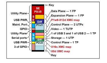
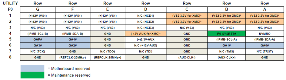
P0 - Utility plane. Contains the following signal definitions:
| Power: | Primary +12V, 3.3V (for non-NAI XMC only), +3.3V_AUX, -12V_AUX (for non-NAI XMC only) and System GND |
|---|---|
| Geographical Address Pins: | GA0# - GA4#, GAP# |
| Card reset: | SYSRST# signal |
| Non-Volatile Memory Read Only: | NVMRO |
| IPMC: | IMPB-SDA-A, IMPB-SDA-B, IMPB-SCL-A, IMPB-SCL-B |
| VPX AUX/REF CLK: | (Not used) |
P1 - Defined as Data/Expansion/Control Planes (XMC defined I/O secondary)
| High Speed Switched Fabric Interface: | Two fat pipe options (PCIe ver. 3.0 (x1)). |
|---|---|
| Ethernet: | Gig-E port option is available and defined + (See Part Number Designation section) |
P2 - XMC/Built-In I/O (primary)
Rear I/O Utility Plane (P0)
The P0 (Utility) Plane contains the primary power, bus and utility signals for the OpenVPX board. Additionally, several of the user defined pins can be utilized for Geographical Addressing and a parallel SYSRST# signal. Signals defined as N/C currently have no functionality associated and is not required for general operation
Note
VS2 (3.3V) and -12V-AUX are not required for motherboard or 68INT6-N NAI-XMC (function module operation). For 68INT6-S (or -T) customer-installed XMC that require those voltages, they MUST be supplied by the backplane power supply. Additionally, the XMC signal VPWR rail provides +12V (derived from the VS1 backplane power supply).
Rear I/O Data/Expansion/Control Planes (P1)
The 68INT6 contains one Fat Pipe (data plane), one Fat Pipe (expansion plane), and two Ultra-Thin Pipes (control plane). The data and expansion planes specify a high-speed serial interface fabric bus connection - PCIe ver.3.0 (x1). The control plane commands the 68INT6 via Gig-E (option for a 10GBase-KR (SerDes) Interface). Pin-outs for a standard VITA 61/42 XMC site (P1w9-P1w14) or optional NAI-XMC w/module (MOD1 I/O) are also defined on the P1 I/O plane. Signals defined as N/C currently have no functionality associated or are considered optional and are not required for general operation.
Standard VITA 61/VITA 42 XMC Site (P1)
| Data Plane | Row | Row | Row | Row | Row | Row | Row |
| P1 | G | F | E | D | C | B | A |
| 1 | GDiscrete1 | GND | VPX-DP0-TXN | VPX-DP0-TXP | GND | VPX-DP0-RXN | VPX-DP0-RXP |
| VPX-PCIE1-TXN | VPX-PCIE1-TXP | VPX-PCIE1-RXN | VPX-PCIE1-RXP | ||||
| 2 | GND | VPX-DP1-TXN | VPX-DP1-TXP | GND | VPX-DP1-RXN | VPX-DP1-RXP | GND |
| VPX-PCIE2-TXN | VPX-PCIE2-TXP | VPX-PCIE2-RXN | VPX-PCIE2-RXP | ||||
| 3 | RTC-STDBY | GND | VPX-DP2-TXN | VPX-DP2-TXP | GND | VPX-DP2-RXN | VPX-DP2-RXP |
| VPX-PCIE3-TXN | VPX-PCIE3-TXP | VPX-PCIE3-RXN | VPX-PCIE3-RXP | ||||
| 4 | GND | VPX-DP3-TXN | VPX-DP3-TXP | GND | VPX-DP3-RXN | VPX-DP3-RXP | GND |
| VPX-PCIE4-TXN | VPX-PCIE4-TXP | VPX-PCIE4-RXN | VPX-PCIE4-RXP | ||||
| 5 | P1-SYSCONn | GND | VPX-EP0-TXN | VPX-EP0-TXP | GND | VPX-EP0-RXN | VPX-EP0-RXP |
| VPX-PCIE5-TXN | VPX-PCIE5-TXP | VPX-PCIE5-RXN | VPX-PCIE5-RXP | ||||
| 6 | GND | VPX-EP1-TXN | VPX-EP1-TXP | GND | VPX-EP1-RXN | VPX-EP1-RXP | GND |
| VPX-PCIE6-TXN | VPX-PCIE6-TXP | VPX-PCIE6-RXN | VPX-PCIE6-RXP | ||||
| 7 | +5-USB3-1 | GND | VPX-EP2-TXN | VPX-EP2-TXP | GND | VPX-EP2-RXN | VPX-EP2-RXP |
| VPX-PCIE7-TXN | VPX-PCIE7-TXP | VPX-PCIE7-RXN | VPX-PCIE7-RXP | ||||
| 8 | GND | VPX-EP3-TXN | VPX-EP3-TXP | GND | VPX-EP3-RXN | VPX-EP3-RXP | GND |
| VPX-PCIE8-TXN | VPX-PCIE8-TXP | VPX-PCIE8-RXN | VPX-PCIE8-RXP | ||||
| 9 | SER-TXD1 | GND | XMCJ16-A5 | XMCJ16-B5 | GND | XMCJ16-D5 | XMCJ16-E5 |
| 10 | GND | XMCJ16-A7 | XMCJ16-B7 | GND | XMCJ16-D7 | XMCJ16-E7 | GND |
| 11 | SER-RXD1 | GND | XMCJ16-A9 | XMCJ16-B9 | GND | XMCJ16-D9 | XMCJ16-E9 |
| 12 | GND | XMCJ16-A15 | XMCJ16-B15 | GND | XMCJ16-D15 | XMCJ16-E15 | GND |
| 13 | TTL-CH1 | GND | XMCJ16-A17 | XMCJ16-B17 | GND | XMCJ16-D17 | XMCJ16-E17 |
| 14 | GND | XMCJ16-A19 | XMCJ16-B19 | GND | XMCJ16-D19 | XMCJ16-E19 | GND |
| 15 | MRSTn | GND | KR-Tx1N | KR-Tx1P | GND | KR-Rx1N | KR-Rx1P |
| 16 | GND | KR-Tx0N | KR-Tx0P | GND | KR-Rx0N | KR-Rx0P | GND |
| = USB 3.1 (Gen 1) | = Expansion Plane: PCIe (Gen 3) | = X12d XMC Map | |||
| = Motherboard reserved | = Combined Plane: PCIe (Tx) | = 10GBase-KR | |||
| = RS-232 Maintenance | = Combined Plane: PCIe (Rx) | ||||
| = Data Plane: PCIe (Gen 3) | = GPIO (TTL default) | ||||
Optional NAI COSA XMC w/Modules (P1)
| Data Plane | Row | Row | Row | Row | Row | Row | Row |
| P1 | G | F | E | D | C | B | A |
| 1 | GDiscrete1 | GND | VPX-DP0-TXN | VPX-DP0-TXP | GND | VPX-DP0-RXN | VPX-DP0-RXP |
| VPX-PCIE1-TXN | VPX-PCIE1-TXP | VPX-PCIE1-RXN | VPX-PCIE1-RXP | ||||
| 2 | GND | VPX-DP1-TXN | VPX-DP1-TXP | GND | VPX-DP1-RXN | VPX-DP1-RXP | GND |
| VPX-PCIE2-TXN | VPX-PCIE2-TXP | VPX-PCIE2-RXN | VPX-PCIE2-RXP | ||||
| 3 | RTC-STDBY | GND | VPX-DP2-TXN | VPX-DP2-TXP | GND | VPX-DP2-RXN | VPX-DP2-RXP |
| VPX-PCIE3-TXN | VPX-PCIE3-TXP | VPX-PCIE3-RXN | VPX-PCIE3-RXP | ||||
| 4 | GND | VPX-DP3-TXN | VPX-DP3-TXP | GND | VPX-DP3-RXN | VPX-DP3-RXP | GND |
| VPX-PCIE4-TXN | VPX-PCIE4-TXP | VPX-PCIE4-RXN | VPX-PCIE4-RXP | ||||
| 5 | P1-SYSCONn | GND | VPX-EP0-TXN | VPX-EP0-TXP | GND | VPX-EP0-RXN | VPX-EP0-RXP |
| VPX-PCIE5-TXN | VPX-PCIE5-TXP | VPX-PCIE5-RXN | VPX-PCIE5-RXP | ||||
| 6 | GND | VPX-EP1-TXN | VPX-EP1-TXP | GND | VPX-EP1-RXN | VPX-EP1-RXP | GND |
| VPX-PCIE6-TXN | VPX-PCIE6-TXP | VPX-PCIE6-RXN | VPX-PCIE6-RXP | ||||
| 7 | +5-USB3-1 | GND | VPX-EP2-TXN | VPX-EP2-TXP | GND | VPX-EP2-RXN | VPX-EP2-RXP |
| VPX-PCIE7-TXN | VPX-PCIE7-TXP | VPX-PCIE7-RXN | VPX-PCIE7-RXP | ||||
| 8 | GND | VPX-EP3-TXN | VPX-EP3-TXP | GND | VPX-EP3-RXN | VPX-EP3-RXP | GND |
| VPX-PCIE8-TXN | VPX-PCIE8-TXP | VPX-PCIE8-RXN | VPX-PCIE8-RXP | ||||
| 9 | SER-TXD1 | GND | MOD1-DATIO01 | MOD1-DATIO02 | GND | MOD1-DATIO03 | MOD1-DATIO04 |
| 10 | GND | MOD1-DATIO05 | MOD1-DATIO06 | GND | MOD1-DATIO07 | MOD1-DATIO08 | GND |
| 11 | SER-RXD1 | GND | MOD1-DATIO09 | MOD1-DATIO10 | GND | MOD1-DATIO11 | MOD1-DATIO12 |
| 12 | GND | MOD1-DATIO13 | MOD1-DATIO14 | GND | MOD1-DATIO15 | MOD1-DATIO16 | GND |
| 13 | TTL-CH1 | GND | MOD1-DATIO17 | MOD1-DATIO18 | GND | MOD1-DATIO19 | MOD1-DATIO20 |
| 14 | GND | MOD1-DATIO21 | MOD1-DATIO22 | GND | MOD1-DATIO23 | MOD1-DATIO24 | GND |
| 15 | MRSTn | GND | KR-Tx1N | KR-Tx1P | GND | KR-Rx1N | KR-Rx1P |
| 16 | GND | KR-Tx0N | KR-Tx0P | GND | KR-Rx0N | KR-Rx0P | GND |
| = USB 3.1 (Gen 1) | = Expansion Plane: PCIe (Gen 3) | = MOD1 I/O (NAI-XMC Option) | |||
| = Motherboard reserved | = Combined Plane: PCIe (Tx) | = 10GBase-KR | |||
| = RS-232 Maintenance | = Combined Plane: PCIe (Rx) | ||||
| = Data Plane: PCIe (Gen 3) | = GPIO (TTL default) | ||||
XMC/Built-In I/O - Defined Area (P2)
The 68INT6 contains no ‘user defined’ I/O data area pin-outs. Pin-outs for a standard VITA 61/42 XMC site (P2w9-P2w16) or optional NAI-XMC w/module (MOD2-I/O) are defined on the P2 I/O plane. In addition to the XMC, there are pin-outs defined for video, USB 2.0 & 3.1, one storage Ultra-Thin Pipe (SATA), and one control plane Thin Pipe (Ethernet). Signals defined as N/C currently have no functionality associated or are considered optional and are not required for general operation.
Standard VITA 61/VITA 42 XMC Site (P2)
| Data Plane | Row | Row | Row | Row | Row | Row | Row |
| P2 | G | F | E | D | C | B | A |
| 1 | SER-TXD0 | GND | DDP-B1-DN | DDP-B1-DP | GND | DDP-B0-DN | DDP-B0-DP |
| 2 | GND | DDP-B3-DN | DDP-B3-DP | GND | DDP-B2-DN | DDP-B2-DP | GND |
| 3 | SER-TXD1 | GND | VID-PWR | HDMI-HPD | GND | HDMI-SDA-AUXN | HDMI-SCL-AUXP |
| 4 | GND | USB2N | USB2P | GND | USB1N | USB1P | GND |
| 5 | SER-RXD0 | GND | USB1-SSTXN | USB1-SSTXP | GND | USB1-SSRXN | USB1-SSRXP |
| 6 | GND | VPX-SATA1-TXN | VPX-SATA1-TXP | GND | VPX-SATA1-RXN | VPX-SATA1-RXN | GND |
| 7 | SER-RXD1 | GND | ETH2-TP1N | ETH2-TP1P | GND | ETH2-TP0N | ETH2-TP0P |
| 8 | GND | ETH2-TP3N | ETH2-TP3P | GND | ETH2-TP2N | ETH2-TP2P | GND |
| 9 | +5V-USB2 | GND | XMCJ16-C12 | XMCJ16-C13 | GND | XMCJ16-F12 | XMCJ16-F13 |
| 10 | GND | XMCJ16-C14 | XMCJ16-C15 | GND | XMCJ16-F14 | XMCJ16-F15 | GND |
| 11 | TTL-CH2 | GND | XMCJ16-C16 | XMCJ16-C17 | GND | XMCJ16-F16 | XMCJ16-F17 |
| TAMPER DETECT | |||||||
| 12 | GND | XMCJ16-C18 | XMCJ16-C19 | GND | XMCJ16-F18 | XMCJ16-F19 | GND |
| 13 | TTL-CH3 | GND | XMCJ16-A1 | XMCJ16-B1 | GND | XMCJ16-D1 | XMCJ16-E1 |
| I2C-SDA | |||||||
| 14 | GND | XMCJ16-A3 | XMCJ16-B3 | GND | XMCJ16-D3 | XMCJ16-E3 | GND |
| 15 | TTL-CH4 | GND | XMCJ16-A11 | XMCJ16-B11 | GND | XMCJ16-D11 | XMCJ16-E11 |
| I2C-SCL | |||||||
| 16 | GND | XMCJ16-A13 | XMCJ16-B13 | GND | XMCJ16-D13 | XMCJ16-E13 | GND |
| = 1x RS-232 or 2x RS422/485 (programmable) | = GPIO (TTL default) | = X16s XMC Map | |||
| = USB 3.1 (Gen 1) / USB 2.0 | = GPIO (Tamper Detect/I2C optional) | = X8d XMC Map | |||
| = SATA III | = Video: DisplayPort (DDI) HDMI | = 1GBase-T |
Optional NAI COSA XMC w/Modules (P2)
| Data Plane | Row | Row | Row | Row | Row | Row | Row |
| P2 | G | F | E | D | C | B | A |
| 1 | SER-TXD0 | GND | DDP-B1-DN | DDP-B1-DP | GND | DDP-B0-DN | DDP-B0-DP |
| 2 | GND | DDP-B3-DN | DDP-B3-DP | GND | DDP-B2-DN | DDP-B2-DP | GND |
| 3 | SER-TXD1 | GND | VID-PWR | HDMI-HPD | GND | HDMI-SDA-AUXN | HDMI-SCL-AUXP |
| 4 | GND | USB2N | USB2P | GND | USB1N | USB1P | GND |
| 5 | SER-RXD0 | GND | USB1-SSTXN | USB1-SSTXP | GND | USB1-SSRXN | USB1-SSRXP |
| 6 | GND | VPX-SATA1-TXN | VPX-SATA1-TXP | GND | VPX-SATA1-RXN | VPX-SATA1-RXN | GND |
| 7 | SER-RXD1 | GND | ETH2-TP1N | ETH2-TP1P | GND | ETH2-TP0N | ETH2-TP0P |
| 8 | GND | ETH2-TP3N | ETH2-TP3P | GND | ETH2-TP2N | ETH2-TP2P | GND |
| 9 | +5V-USB2 | GND | MOD2-DATIO05 | MOD2-DATIO06 | GND | MOD2-DATIO11 | MOD2-DATIO12 |
| 10 | GND | MOD2-DATIO17 | MOD2-DATIO18 | GND | MOD2-DATIO29 | MOD2-DATIO30 | GND |
| SPK-LP+ | SPK-LN+ | ||||||
| 11 | TTL-CH2 | GND | MOD2-DATIO19 | MOD2-DATIO20 | GND | MOD2-DATIO21 | MOD2-DATIO22 |
| TAMPER DETECT | |||||||
| 12 | GND | MOD2-DATIO23 | MOD2-DATIO24 | GND | MOD2-DATIO31 | MOD2-DATIO32 | GND |
| SPK-RP+ | SPK-RN+ | ||||||
| 13 | TTL-CH3 | GND | MOD2-DATIO01 | MOD2-DATIO02 | GND | MOD2-DATIO03 | MOD2-DATIO04 |
| I2C-SDA | |||||||
| 14 | GND | MOD2-DATIO13 | MOD2-DATIO14 | GND | MOD2-DATIO25 | MOD2-DATIO26 | GND |
| HEADPHONE-R+ | HEADPHONE-L+ | ||||||
| 15 | TTL-CH4 | GND | MOD2-DATIO07 | MOD2-DATIO08 | GND | MOD2-DATIO09 | MOD2-DATIO10 |
| I2C-SCL | |||||||
| 16 | GND | MOD2-DATIO15 | MOD2-DATIO16 | GND | MOD2-DATIO27 | MOD2-DATIO28 | GND |
| MIC / VREFOUT-A+ | GND+ |
| = 1x RS-232 or 2x RS422/485 (programmable) | = GPIO (TTL default) | = MOD2 I/O (NAI-XMC Option) | |||
| = USB 3.1 (Gen 1) / USB 2.0 | = GPIO (Tamper Detect/I2C optional) | = SATA III | |||
| = Video: DisplayPort (DDI) HDMI | = 1GBase-T | = Audio headset MIC/Headphones | |||
| = Audio SPK L, R |
Note
For a more detailed breakdown of the P2 pinouts for the programmable RS232 or RS-422/48 configurations, please refer to the table below:
| Plane/Row | 2x RS-232 ports | 1x RS-422/485 port |
| P2-G1 | SER-TDX0 | -SER-TDX1 |
| P2-G5 | SER-RDX0 | -SER-RDX1 |
| P2-G3 | SER-TDX1 | SER-TDX1 |
| P2-G7 | SER-RDX1 | SER-RDX1 |
+NAI’s XMC board is capable of being configured with an audio codec with allows users to order a 68INT6 with the following audio configurations:
- 68INT6-A: NAI XMC w/Audio headset MIC & Headphones
- 68INT6-B: NAI XMC w/Audio SPK L, R
- 68INT6-C: NAI XMC w/Audio Headset & Speakers
The audio codec enables pinout signals on Module Slot 2 in lieu of MOD2-DATIO25-28 and are defined as follows:
| XMC/Built-In I/O Plane – Defined Area (P2) | 68INT6 NAI-XMC Audio Options | ||||
| User Defined Plane Pin | Replaced MOD2-DATIO Pin | Audio Signal Description | 68INT6-A + (Headset) | 68INT6-B + (Speakers) | 68INT6-C + (Speakers & Headset) |
| P2-C14 | MOD2-DATIO25 | Right Headphone | X | - | X |
| P2-B14 | MOD2-DATIO26 | Left Headphone | X | - | X |
| P2-C16 | MOD2-DATIO27 | Microphone Output reference voltage | X | - | X |
| P2-B16 | MOD2-DATIO28 | Ground (Headset Detect) | X | - | X |
| P2-C10 | MOD2-DATIO29 | Left Speaker (+) | - | X | X |
| P2-B10 | MOD2-DATIO30 | Left Speaker (-) | - | X | X |
| P2-C12 | MOD2-DATIO31 | Right Speaker (+) | - | X | X |
| P2-C12 | MOD2-DATIO32 | Right Speaker (-) | - | X | X |
Note
The max impedance for the MIC/Headphones is 660 ohms; the max impedance for the speakers is 3.3 ohms.
Note
Output reference voltage is an additional signal on MOD2-DATIO pin 27. Pin 27 is a dual-purpose pin; it is AC-coupled for single microphone signal input and is DC-coupled to provide power to an external microphone. It provides 0.5 V.
68INT6 Standard VITA 61/VITA 42 XMC Site PCIe Pinouts
| XMC | Row | Row | Row | Row | Row | Row |
| J15 | F | E | D | C | B | A |
| 1 | +12V-XMC | XMC-PCIe-TX1N + (CPU-PCIe4-RX1N) | XMC-PCIe-TX1P + (CPU-PCIe4-RX1P) | +3.3V-XMC | XMC-PCIe-TX0N + (CPU-PCIe4-RX0N) | XMC-PCIe-TX0P + (CPU-PCIe4-RX0P) |
| 2 | XMC-MRSTIn | GND | GND | XMC-TRSTn | GND | GND |
| 3 | +12V-XMC | XMC-PCIe-TX3N + (CPU-PCIe4-RX3N) | XMC-PCIe-TX3P + (CPU-PCIe4-RX3P) | +3.3V-XMC | XMC-PCIe-TX2N + (CPU-PCIe4-RX2N) | XMC-PCIe-TX2P + (CPU-PCIe4-RX2P) |
| 4 | XMC-MRST0n | GND | GND | N/C | GND | GND |
| 5 | +12V-XMC | N/C | N/C | +3.3V-XMC | XMC-PCIe-TX4N + (PCH-PCIe10-RXN) | XMC-PCIe-TX4P + (PCH-PCIe10-RXP) |
| 6 | +12V-XMC | GND | GND | N/C | GND | GND |
| 7 | +12V-XMC | N/C | N/C | +3.3V-XMC | N/C | N/C |
| 8 | -12V-XMC | GND | GND | N/C | GND | GND |
| 9 | +12V-XMC | MOD2-PCIE16SATA3-RXN + (MOD2-SATA1-TXN) | MOD2-PCIE16SATA3-RXP + (MOD2-SATA1-TXP) | N/C | MOD2-PCIE16SATA3-TXN + (MOD2-SATA1-RXN) | MOD2-PCIE16SATA3-TXP + (MOD2-SATA1-RXP) |
| 10 | GND (XMC-GA0) | GND | GND | N/C | GND | GND |
| 11 | +12V-XMC | XMC-PCIe-RX1N + (CPU-PCIe4-TX1N) | XMC-PCIe-RX1P + (CPU-PCIe4-TX1P) | XMC-MBISTn | XMC-PCIe-RX0N + (CPU-PCIe4-TX0N) | XMC-PCIe-RX0P + (CPU-PCIe4-TX0P) |
| 12 | XMC-MPRESENTn | GND | GND | GND + (XMC-GA1) | GND | GND |
| 13 | +12V-XMC | XMC-PCIe-RX3N + (CPU-PCIe4-TX3N) | XMC-PCIe-RX3P + (CPU-PCIe4-TX3P) | +3.3V-AUX | XMC-PCIe-RX2N + (CPU-PCIe4-TX2N) | XMC-PCIe-RX2P + (CPU-PCIe4-TX2P) |
| 14 | MO-SDA | GND | GND | GND + (XMC-GA2) | GND | GND |
| 15 | +12V-XMC | N/C | N/C | N/C | XMC-PCIe04-RXN + (PCH-PCIe10-TXN) | XMC-PCIe04-RXP + (PCH-PCIe10-TXP) |
| 16 | MO-SCL | GND | GND | XMC-NVMRO | GND | GND |
| 17 | N/C | N/C | N/C | N/C | N/C | N/C |
| 18 | N/C | GND | GND | N/C | GND | GND |
| 19 | N/C | N/C | PCH-PCIe-WAKEn | N/C | XMC-PCIe-REFCLKN | XMC-PCIe-REFCLKP |
Rear User I/O Mapping (NAI-XMC Configuration Option Only)
Pin-out details (for reference) are shown below, with respect to DATAIO. Additional information on pin-outs can be found in the Module Operational Manuals
| Slot 1 | Slot 2 | |||
| Module Signal (Ref Only) | Rear I/O P1 | Global (MB) | Rear I/O P2 | Global (MB) |
| DATIO1 | E09 | E13 | ||
| DATIO2 | D09 | D13 | ||
| DATIO3 | B09 | B13 | ||
| DATIO4 | A09 | A13 | ||
| DATIO5 | F10 | E09 | ||
| DATIO6 | E10 | D09 | ||
| DATIO7 | C10 | E15 | ||
| DATIO8 | B10 | D15 | ||
| DATIO9 | E11 | B15 | ||
| DATIO10 | D11 | A15 | ||
| DATIO11 | B11 | B09 | ||
| DATIO12 | A11 | A09 | ||
| DATIO13 | F12 | F14 | ||
| DATIO14 | E12 | E14 | ||
| DATIO15 | C12 | F16 | ||
| DATIO16 | B12 | E16 | ||
| DATIO17 | E13 | F10 | ||
| DATIO18 | D13 | E10 | ||
| DATIO19 | B13 | E11 | ||
| DATIO20 | A13 | D11 | ||
| DATIO21 | F14 | B11 | ||
| DATIO22 | E14 | A11 | ||
| DATIO23 | C14 | F12 | ||
| DATIO24 | B14 | E12 | ||
| DATIO25 | C14 | |||
| DATIO26 | B14 | |||
| DATIO27 | C16 | |||
| DATIO28 | B16 | |||
| DATIO29 | C10 | |||
| DATIO30 | B10 | |||
| DATIO31 | C12 | |||
| DATIO32 | B12 | |||
| DATIO33 | ||||
| DATIO34 | ||||
| DATIO35 | ||||
| DATIO36 | ||||
| DATIO37 | ||||
| DATIO38 | ||||
| DATIO39 | ||||
| DATIO40 | ||||
| N/A | SYS GND | SYS GND | ||
| CHASSIS | CHASSIS | |||
| N/C | N/C | |||
MECHANICAL
General Outline
Note
The following mechanical outline detail examples are provided for reference only. Dimensions are in inches unless otherwise specified.
Conduction-Cooled
68INT6 PART NUMBER DESIGNATION
Click here for the 68INT6 part number designation
APPENDIX: NAI-XMC CONFIGURATION OPTION
When configured with the optional NAI-XMC mezzanine site, the 68INT6 can support up to two independent, smart function modules based on NAI’s COSA® architecture. With over 100 modules to choose from, this option further expands the SBC’s capabilities beyond the standard XMC site, providing a perfect solution for SOSA™-aligned rugged commercial, industrial, and aerospace applications.
Register Memory Map Addressing
The register map address consists of the following:
• cPCI/PCIe BAR or Base Address for the Board • Module Slot Base Address • Function Offset Address
Board Base Address
The table below lists the BAR used for access to the motherboard and module registers. The second BAR is used internally for motherboard and module firmware updates. The other cPCI/PCIe BARs not listed are not used.
| NAI Boards | Device ID | Bus | Motherboard and Module Register Access | Motherboard and Module Firmware Updates |
| Controller/Master Boards | ||||
| 68INT6 | N/A | PCIe | BAR 1 Size: Module Dependent (minimum 64K bytes) | BAR 2 Size: 1M bytes |
Module Slot and Function Addresses
The memory map for the modules are dependent on the types of modules on the board and the order in which the modules are installed on the board as well as the firmware installed on the motherboard. The function modules are enumerated allowing for dynamic memory space allocation and therefore the “start” address of the module function register area is factory pre-defined (and read from) the Module Address register. Refer to Figure 1 for an example.
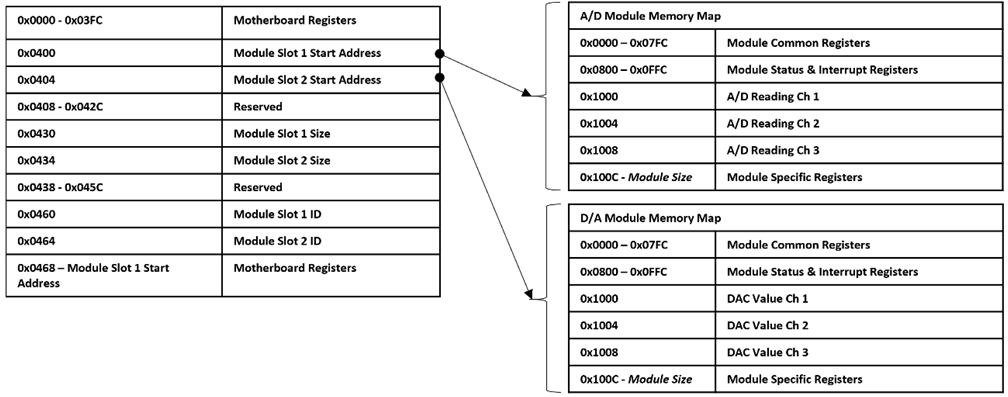 Figure 1. Register Memory Map Addressing for Motherboards with 2 Modules
Address Calculation
Motherboard Registers:
Read/Write access to the motherboard registers starts with the base address for the board and then the motherboard base offset address.
For example, to address Module Slot 1 Start Address register (i.e. register address = 0x0400):
- Start with the base address for the board.
- Add the motherboard base register address offset.
| Motherboard Address = | Base Address Motherboard Address Offset | = 0x0000 0400 |
| 0x0000 0000 + 0x0400 |
Module Registers:
Read/Write access to the Function module’s registers start with the base address of the board. Add the “content” for the Module Start Address and then, add the specific module function register offset.
For example, to address an appropriate/specific function module with a register offset:
- Start with the base address for the board.
- Add the value (contents) from the module base address offset register (contents/value of Motherboard Memory register for Module 1 (i.e., @ 0x0400) = 0x4000.
- Then add the specific module function Register Offset of interest (i.e., A/D Reading Ch 1 @ 0x1000)
| (Function Specific) Address = | Base Address + | Module Base Address Offset + | Function Register Offset | = 0x0000 5000 |
| 0x0000 0000 | 0x4000 | 0x1000 |
Register Descriptions
Module Information Registers
The Module Slot Addressing Ready, Module Slot Address, Module Slot Size and Module Slot ID registers provide information about the modules detected on the board.
Module Slot Addressing Ready
| Function: | Indicates that the module slots are ready to be addressed. |
|---|---|
| Type: | unsigned binary word (32-bit) |
| Data Range: | 0x0000 0000 to 0xFFFF FFFF |
| Read/Write: | R |
| Initialized Value: | 0xA5A5A5A5 |
| Operational Settings: | This register will contain the value of 0xA5A5A5A5 when the module addresses have been determined. |
Module Slot Address
| Function: | Specifies the Base Address for the module in the specific slot position. |
|---|---|
| Type: | unsigned binary word (32-bit) |
| Data Range: | 0x0000 0000 to 0xFFFF FFFF |
| Read/Write: | R |
| Initialized Value: | Based on board’s module configuration. |
| Operational Settings: | 0x0000 0000 indicates no Module found. |
Module Slot Size
| Function: | Specifies the Memory Size (in bytes) allocated for the module in the specific slot position. |
|---|---|
| Type: | unsigned binary word (32-bit) |
| Range: | 0x0000 0000 to 0xFFFF FFFF |
| Read/Write: | R |
| Initialized Value: | Assigned by factory for the module. |
| Operational Settings: | 0x0000 0000 indicates no Module found. |
Module Slot ID
| Function: | Specifies the Model ID for the module in the specified slot position. |
|---|---|
| Type: | 4-character ASCII string |
| Data Range: | 0x0000 0000 to 0xFFFF FFFF |
| Read/Write: | R |
| Initialized Value: | Assigned by factory for the module. |
| Operational Settings: | The Module ID is formatted as four ASCII bytes: three characters followed by a space. Module IDs are in little-endian order with a single space following the first three characters. For example, ‘TL1’ is ‘1LT’, ‘SC1’ is ‘1CS’ and so forth. Example below is for “TL1” (MSB justified). All value of 0000 0000 indicates no Module found. |
| D31 | D30 | D29 | D28 | D27 | D26 | D25 | D24 | D23 | D22 | D21 | D20 | D19 | D18 | D17 | D16 |
| ASCII Character (ex: 'T' - 0x54) | ASCII Character (ex: 'L' - 0x4C) | ||||||||||||||
| D15 | D14 | D13 | D12 | D11 | D10 | D9 | D8 | D7 | D6 | D5 | D4 | D3 | D2 | D1 | D0 |
| ASCII Character (ex: '1' - 0x31) | ASCII Space (' ' - 0x20) | ||||||||||||||
Hardware Information Registers
The registers identified in this section provide information about the board’s hardware.
Product Serial Number
| Function: | Specifies the Board Serial Number. |
|---|---|
| Type: | unsigned binary word (32-bit) |
| Data Range: | 0x0000 0000 to 0xFFFF FFFF |
| Read/Write: | R |
| Initialized Value: | Serial number assigned by factory for the board. |
| Operational Settings: | N/A |
Platform
| Function: | Specifies the Board Platform Identifier. Values are for the ASCII characters for the NAI valid platforms (Identifiers). |
|---|---|
| Type: | 4-character ASCII string |
| Data Range: | See table below. |
| Read/Write: | R |
| Initialized Value: | ASCII code is for the Platform Identifier of the board |
| Operational Settings: | NAI platform for this board is shown below: |
| NAI Platform | Platform Identifier | 4-character ASCII String |
|---|---|---|
| 3U VPX | 68 | 0x0000 3836 |
Model
| Function: | Specifies the Board Model Identifier. Values are for the ASCII characters for the NAI valid models. |
|---|---|
| Type: | 4-character ASCII string |
| Data Range: | See table below. |
| Read/Write: | R |
| Initialized Value: | ASCII code is for the Model Identifier of the board |
| Operational Settings: | NAI model for this board is shown below: |
| NAI Model | 4-character ASCII String |
|---|---|
| INT | 0x0054 4E49 |
Generation
| Function: | Specifies the Board Generation. Identifier values are for the ASCII characters for the NAI valid generation identifiers. |
|---|---|
| Type: | 4-character ASCII string |
| Data Range: | See table below. |
| Read/Write: | R |
| Initialized Value: | ASCII code is for the Generation Identifier of the board |
| Operational Settings: | NAI generation for this board is shown below: |
| NAI Generation | 4-character ASCII String |
|---|---|
| 6 | 0x0000 0036 |
Ethernet Interface Count/Processor Count
| Function: | Specifies the Ethernet Interface Count and Processor Count |
|---|---|
| Type: | unsigned binary word (32-bit) |
| Data Range: | See table below. |
| Read/Write: | R |
| Operational Settings: | Ethernet Interface Count - Indicates the number of Ethernet interfaces on the product motherboard. + For example, Single Ethernet = 1; Dual Ethernet = 2 Processor Count - Indicates the number of unique processor types on the motherboard = 2 |
| NAI Board | Processor Count | Description | |
| 3U-VPX | 68INT6 | 2 | Four-Core Intel i7-118xGRE Xilinx Zynq 7015 with Dual Core Cortex A9 |
| D31 | D30 | D29 | D28 | D27 | D26 | D25 | D24 | D23 | D22 | D21 | D20 | D19 | D18 | D17 | D16 |
| Ethernet Interface Count (Based on Part Number Ethernet Options) | |||||||||||||||
| D15 | D14 | D13 | D12 | D11 | D10 | D9 | D8 | D7 | D6 | D5 | D4 | D3 | D2 | D1 | D0 |
| Processor Count (0x0002) | |||||||||||||||
Maximum Module Slot Count/ARM Platform Type
| Function: | Specifies the Maximum Module Slot Count and ARM Platform Type. |
|---|---|
| Type: | unsigned binary word (32-bit) |
| Data Range: | See table below. |
| Read/Write: | R |
| Operational Settings: | Maximum Module Slot Count - Indicates the number of modules that can be installed on the product. ARM Platform - Altera = 1; Xilinx X1 = 2; Xilinx X2 = 3; UltraScale = 4 |
| NAI Board | Maximum Module Slot Count | ARM Platform Type | |
| 3U-VPX | 68INT6 | 2 | Xilinx X2 = 3 |
| D31 | D30 | D29 | D28 | D27 | D26 | D25 | D24 | D23 | D22 | D21 | D20 | D19 | D18 | D17 | D16 |
| ARM Platform Type (See Table) | |||||||||||||||
| D15 | D14 | D13 | D12 | D11 | D10 | D9 | D8 | D7 | D6 | D5 | D4 | D3 | D2 | D1 | D0 |
| Maximum Module Slot Count (See Table) | |||||||||||||||
Motherboard Firmware Information Registers
The registers in this section provide information on the revision of the firmware installed on the motherboard.
Motherboard Core Firmware Version
| Function: | Specifies the Version of the NAI factory provided Motherboard Core Application installed on the board. |
|---|---|
| Type: | Two (2) unsigned binary word (32-bit) |
| Data Range: | 0x0000 0000 to 0xFFFF FFFF |
| Read/Write: | R |
| Operational Settings: | The motherboard firmware version consists of four components: + Major, Minor, Minor 2 and Minor 3. |
| Motherboard Core Firmware Version (Note: little-endian order in register) (ex. 4.7.0.0) | |||||||||||||||
| Word 1 (Ex. 0007 0004 = 4.7 (Major.Minor) | |||||||||||||||
| D31 | D30 | D29 | D28 | D27 | D26 | D25 | D24 | D23 | D22 | D21 | D20 | D19 | D18 | D17 | D16 |
| Minor (ex: 0x0007 = 7) | |||||||||||||||
| D15 | D14 | D13 | D12 | D11 | D10 | D9 | D8 | D7 | D6 | D5 | D4 | D3 | D2 | D1 | D0 |
| Major (ex: 0x0004 = 4) | |||||||||||||||
| Word 2 (Ex. 0x0000 0000 = 0000 = 0.0 (Minor2.Minor3)) | |||||||||||||||
| D31 | D30 | D29 | D28 | D27 | D26 | D25 | D24 | D23 | D22 | D21 | D20 | D19 | D18 | D17 | D16 |
| Minor 3 (ex: 0x000 = 0) | |||||||||||||||
| D15 | D14 | D13 | D12 | D11 | D10 | D9 | D8 | D7 | D6 | D5 | D4 | D3 | D2 | D1 | D0 |
| Minor 2 (ex: 0x000 = 0) | |||||||||||||||
Motherboard Core Build Time/Date
| Function: | Specifies the Build Date/Time of the NAI factory provided Motherboard Core Application installed on the board. |
|---|---|
| Type: | Two (2) unsigned binary word (32-bit) |
| Data Range: | N/A |
| Read/Write: | R |
| Operational Settings: | The motherboard firmware time consists of the Build Date and Build Time. |
| Motherboard Core Build Time (Note: little-endian order in register) | |||||||||||||||
| Word 1 - Build Date (ex. 0x030C 07E2 = 2018-12-03) | |||||||||||||||
| D31 | D30 | D29 | D28 | D27 | D26 | D25 | D24 | D23 | D22 | D21 | D20 | D19 | D18 | D17 | D16 |
| Day (ex: 0x03 = 3) | Month (ex: 0x0C = 12) | ||||||||||||||
| D15 | D14 | D13 | D12 | D11 | D10 | D9 | D8 | D7 | D6 | D5 | D4 | D3 | D2 | D1 | D0 |
| Year (ex: 0x07E2 = 2018) | |||||||||||||||
| Word 2 - Build Time (ex. 0x001B 3B0A = 10:59:27) | |||||||||||||||
| D31 | D30 | D29 | D28 | D27 | D26 | D25 | D24 | D23 | D22 | D21 | D20 | D19 | D18 | D17 | D16 |
| null (0x00) | Seconds (ex: 0x1B = 27) | ||||||||||||||
| D15 | D14 | D13 | D12 | D11 | D10 | D9 | D8 | D7 | D6 | D5 | D4 | D3 | D2 | D1 | D0 |
| Minutes (ex: 0x3B = 59) | Hours (ex: 0x0A = 10) | ||||||||||||||
Motherboard Monitoring Registers
The registers in this provide motherboard temperature measurement information, and where applicable the host processor and slave processor measurements.
| NAI Boards | Bus | Has Host Processor | Has Slave Processor |
| Controller/Master Boards | |||
| 68INT6 | PCIe | Yes (Host = Four-Core Intel i7-118xGRE) | No |
Temperature Readings Register
The temperature registers provide the current, maximum (from power-up) and minimum (from power-up) for the processor and PCB for Zynq processor, and for the Host processor.
These registers are only available on Xilinx Generation 5 platforms, and are periodically populated by the motherboard core application, which only runs in Petalinux and BareMetal. For other operating systems, refer to the naibrd Software Support Kit (SSK) naibsp_system_Monitor_Temperature_Get() routine to manually retrieve the temperature (NOTE: this feature is typically utilized for development/factory use only; contact the factory for additional details on potential use, if required).
| Function: | Specifies the Measured Temperatures on Motherboard. |
|---|---|
| Type: | signed byte (8-bits) for each temperature reading - Six (6) 32-bit words |
| Data Range: | 0x0000 0000 to 0xFFFF 0000 |
| Read/Write: | R |
| Initialized Value: | Value corresponding to the measured temperatures based on the table below. |
| Operational Settings: | The 8-bit temperature readings are signed bytes. For example, if the following register contains the value 0x6955 0000: |
Example:
| Word 3 (Max Zynq Temperatures) | |||||||||||||||
| D31 | D30 | D29 | D28 | D27 | D26 | D25 | D24 | D23 | D22 | D21 | D20 | D19 | D18 | D17 | D16 |
| Max Zynq Core Temperature | Max Zynq PCB Temperature | ||||||||||||||
| D15 | D14 | D13 | D12 | D11 | D10 | D9 | D8 | D7 | D6 | D5 | D4 | D3 | D2 | D1 | D0 |
| 0x00 | 0x00 | ||||||||||||||
The values would represent the following temperatures:
| Temperature Measurements | Data Bits | Value | Temperature (Celsius) |
|---|---|---|---|
| Max Zynq Core Temperature | D31:D24 | 0x69 | +105° |
| Max Zynq PCB Temperature | D23:D16 | 0x55 | +85° |
| Temperature Readings | |||||||||||||||
| Word 1 (Current Zynq Temperatures) | |||||||||||||||
| D31 | D30 | D29 | D28 | D27 | D26 | D25 | D24 | D23 | D22 | D21 | D20 | D19 | D18 | D17 | D16 |
| Zynq Core Temperature | Zynq PCB Temperature | ||||||||||||||
| D15 | D14 | D13 | D12 | D11 | D10 | D9 | D8 | D7 | D6 | D5 | D4 | D3 | D2 | D1 | D0 |
| 0x00 | 0x00 | ||||||||||||||
| Word 2 (Reserved) | |||||||||||||||
| D31 | D30 | D29 | D28 | D27 | D26 | D25 | D24 | D23 | D22 | D21 | D20 | D19 | D18 | D17 | D16 |
| 0x00 | 0x00 | ||||||||||||||
| D15 | D14 | D13 | D12 | D11 | D10 | D9 | D8 | D7 | D6 | D5 | D4 | D3 | D2 | D1 | D0 |
| 0x00 | 0x00 | ||||||||||||||
| Word 3 (Max Zynq Temperatures) | |||||||||||||||
| D31 | D30 | D29 | D28 | D27 | D26 | D25 | D24 | D23 | D22 | D21 | D20 | D19 | D18 | D17 | D16 |
| Max Zynq Core Temperature | Max Zynq PCB Temperature | ||||||||||||||
| D15 | D14 | D13 | D12 | D11 | D10 | D9 | D8 | D7 | D6 | D5 | D4 | D3 | D2 | D1 | D0 |
| 0x00 | 0x00 | ||||||||||||||
| Word 4 (Reserved) | |||||||||||||||
| D31 | D30 | D29 | D28 | D27 | D26 | D25 | D24 | D23 | D22 | D21 | D20 | D19 | D18 | D17 | D16 |
| 0 | 0 | 0 | 0 | 0 | 0 | 0 | 0 | 0 | 0 | 0 | 0 | 0 | 0 | 0 | 0 |
| D15 | D14 | D13 | D12 | D11 | D10 | D9 | D8 | D7 | D6 | D5 | D4 | D3 | D2 | D1 | D0 |
| 0x00 | 0x00 | ||||||||||||||
| Word 5 (Min Zynq Temperatures) | |||||||||||||||
| D31 | D30 | D29 | D28 | D27 | D26 | D25 | D24 | D23 | D22 | D21 | D20 | D19 | D18 | D17 | D16 |
| 0 | 0 | 0 | 0 | 0 | 0 | 0 | 0 | 0 | 0 | 0 | 0 | 0 | 0 | 0 | 0 |
| D15 | D14 | D13 | D12 | D11 | D10 | D9 | D8 | D7 | D6 | D5 | D4 | D3 | D2 | D1 | D0 |
| Min Zynq Core Temperature | Min Zynq PCB Temperature | ||||||||||||||
| Word 6 (Reserved) | |||||||||||||||
| D31 | D30 | D29 | D28 | D27 | D26 | D25 | D24 | D23 | D22 | D21 | D20 | D19 | D18 | D17 | D16 |
| 0 | 0 | 0 | 0 | 0 | 0 | 0 | 0 | 0 | 0 | 0 | 0 | 0 | 0 | 0 | 0 |
| D15 | D14 | D13 | D12 | D11 | D10 | D9 | D8 | D7 | D6 | D5 | D4 | D3 | D2 | D1 | D0 |
| 0x00 | 0x00 | ||||||||||||||
Higher Precision Temperature Readings Register
These registers provide higher precision readings of the current Zynq and PCB temperatures.
Higher Precision Zynq Core Temperature
| Function: | Specifies the Higher Precision Measured Zynq Core temperature on Interface Board. |
|---|---|
| Type: | signed word (16-bits) for integer part and unsigned word (16-bits) for fractional part |
| Data Range: | 0x0000 0000 to 0xFFFF FFFF |
| Read/Write: | R |
| Initialized Value: | Measured Zynq Core temperature on Interface Board |
| Operational Settings: | The upper 16-bits represent the signed integer part of the temperature and the lower 16-bits represent the fractional part of the temperature with the resolution of 1/1000 of degree Celsius. For example, if the register contains the value 0x002B 0271, this represents Zynq Core Temperature = 43.625° Celsius, and value 0xFFF6 0177 represents -10.375° Celsius. |
| D31 | D30 | D29 | D28 | D27 | D26 | D25 | D24 | D23 | D22 | D21 | D20 | D19 | D18 | D17 | D16 |
| Signed Integer Part of Temperature | |||||||||||||||
| D15 | D14 | D13 | D12 | D11 | D10 | D9 | D8 | D7 | D6 | D5 | D4 | D3 | D2 | D1 | D0 |
| Fractional Part of Temperature | |||||||||||||||
Higher Precision Motherboard PCB Temperature
| Function: | Specifies the Higher Precision Measured Motherboard PCB temperature. |
|---|---|
| Type: | signed word (16-bits) for integer part and unsigned word (16-bits) for fractional part |
| Data Range: | 0x0000 0000 to 0xFFFF FFFF |
| Read/Write: | R |
| Initialized Value: | Measured Motherboard PCB temperature |
| Operational Settings: | The upper 16-bits represent the signed integer part of the temperature and the lower 16-bits represent the fractional part of the temperature with the resolution of 1/1000 of degree Celsius. For example, if the register contains the value 0x0020 007D, this represents Interface PCB Temperature = 32.125° Celsius, and value 0xFFE8 036B represents -24.875° Celsius. |
| D31 | D30 | D29 | D28 | D27 | D26 | D25 | D24 | D23 | D22 | D21 | D20 | D19 | D18 | D17 | D16 |
| Signed Integer Part of Temperature | |||||||||||||||
| D15 | D14 | D13 | D12 | D11 | D10 | D9 | D8 | D7 | D6 | D5 | D4 | D3 | D2 | D1 | D0 |
| Fractional Part of Temperature | |||||||||||||||
Motherboard Health Monitoring Registers
The registers in this section provide a summary of motherboard temperature sensors and their corresponding bits. Additionally, this section provides an overview of the registers allocated to those sensors, which are used to monitor current/minimum/maximum temperature readings, upper & lower critical/warning temperature thresholds, and whether or not a programmed temperature threshold has been exceeded.
These registers are only available on Xilinx Generation 5 platforms, and are periodically populated by the motherboard core application, which only runs in Petalinux and BareMetal. For other operating systems, refer to the naibrd Software Support Kit (SSK) naibsp_system_Monitor_Temperature_Get() routine to manually retrieve the temperature (NOTE: this feature is typically utilized for development/factory use only; contact the factory for additional details on potential use, if required).
Motherboard Sensor Summary Status
| Function: | The corresponding sensor bit is set if the sensor has crossed any of its thresholds. |
|---|---|
| Type: | unsigned binary word (32-bits) |
| Data Range: | See table below |
| Read/Write: | R |
| Initialized Value: | 0 |
| Operational Settings: | This register provides a summary for motherboard sensors. When the corresponding sensor bit is set, the Sensor Threshold Status register for that sensor will indicate the threshold condition that triggered the event. |
| Motherboard Sensor Summary Status | |
| Bit(s) | Sensor |
| D4 | Motherboard PCB Temperature |
| D3 | Zynq Core Temperature |
| D2:D0 | Reserved |
Motherboard Sensor Registers
The registers listed in this section apply to each module sensor listed for the Motherboard Sensor Summary Status register. Each individual sensor register provides a group of registers for monitoring motherboard temperatures readings. From these registers, a user can read the current temperature of the sensor in addition to the minimum and maximum temperature readings since power-up. Upper and lower critical/warning temperature thresholds can be set and monitored from these registers. When a programmed temperature threshold is crossed, the Sensor Threshold Status register will set the corresponding bit for that threshold. The figure below shows the functionality of this group of registers when accessing the Zynq Core Temperature sensor as an example.
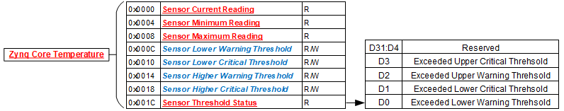
Sensor Threshold Status
| Function: | Reflects which threshold has been crossed |
|---|---|
| Type: | unsigned binary word (32-bits) |
| Data Range: | See table below |
| Read/Write: | R |
| Initialized Value: | 0 |
| Operational Settings: | The associated bit is set when the sensor reading exceed the corresponding threshold settings. |
| Bit(s) | Description |
|---|---|
| D31:4 | Reserved |
| D3 | Exceeded Upper Critical Threshold |
| D2 | Exceeded Upper Warning Threshold |
| D1 | Exceeded Lower Critical Threshold |
| D0 | Exceeded Lower Warning Threshold |
Sensor Current Reading
| Function: | Reflects current reading of temperature sensor |
|---|---|
| Type: | Single Precision Floating Point Value (IEEE-754) |
| Data Range: | Single Precision Floating Point Value (IEEE-754) |
| Read/Write: | R |
| Initialized Value: | N/A |
| Operational Settings: | The register represents current sensor reading as a single precision floating point value. For example, for a temperature sensor, register value 0x41C6 0000 represents temperature = 24.75° Celsius. |
Sensor Minimum Reading
| Function: | Reflects minimum value of temperature sensor since power up |
|---|---|
| Type: | Single Precision Floating Point Value (IEEE-754) |
| Data Range: | Single Precision Floating Point Value (IEEE-754) |
| Read/Write: | R |
| Initialized Value: | N/A |
| Operational Settings: | The register represents minimum sensor value as a single precision floating point value. For example, for a temperature sensor, register value 0x41C6 0000 represents temperature = 24.75° Celsius. |
Sensor Maximum Reading
| Function: | Reflects maximum value of temperature sensor since power up |
|---|---|
| Type: | Single Precision Floating Point Value (IEEE-754) |
| Data Range: | Single Precision Floating Point Value (IEEE-754) |
| Read/Write: | R |
| Initialized Value: | N/A |
| Operational Settings: | The register represents maximum sensor value as a single precision floating point value. For example, for a temperature sensor, register value 0x41C6 0000 represents temperature = 24.75° Celsius. |
Sensor Lower Warning Threshold
| Function: | Reflects lower warning threshold of temperature sensor |
|---|---|
| Type: | Single Precision Floating Point Value (IEEE-754) |
| Data Range: | Single Precision Floating Point Value (IEEE-754) |
| Read/Write: | R/W |
| Initialized Value: | Default lower warning threshold (value dependent on specific sensor) |
| Operational Settings: | The register represents sensor lower warning threshold as a single precision floating point value. For example, for a temperature sensor, register value 0xC220 0000 represents temperature = -40.0° Celsius. |
Sensor Lower Critical Threshold
| Function: | Reflects lower critical threshold of temperature sensor |
|---|---|
| Type: | Single Precision Floating Point Value (IEEE-754) |
| Data Range: | Single Precision Floating Point Value (IEEE-754) |
| Read/Write: | R/W |
| Initialized Value: | Default lower critical threshold (value dependent on specific sensor) |
| Operational Settings: | The register represents sensor lower critical threshold as a single precision floating point value. For example, for a temperature sensor, register value 0xC25C 0000 represents temperature = -55.0° Celsius. |
Sensor Upper Warning Threshold
| Function: | Reflects upper warning threshold of temperature sensor |
|---|---|
| Type: | Single Precision Floating Point Value (IEEE-754) |
| Data Range: | Single Precision Floating Point Value (IEEE-754) |
| Read/Write: | R/W |
| Initialized Value: | Default upper warning threshold (value dependent on specific sensor) |
| Operational Settings: | The register represents sensor upper warning threshold as a single precision floating point value. For example, for a temperature sensor, register value 0x42AA 0000 represents temperature = 85.0° Celsius. |
Sensor Upper Critical Threshold
| Function: | Reflects upper critical threshold of temperature sensor |
|---|---|
| Type: | Single Precision Floating Point Value (IEEE-754) |
| Data Range: | Single Precision Floating Point Value (IEEE-754) |
| Read/Write: | R/W |
| Initialized Value: | Default upper critical threshold (value dependent on specific sensor) |
| Operational Settings: | The register represents sensor upper critical threshold as a single precision floating point value. For example, for a temperature sensor, register value 0x42FA 0000 represents temperature = 125.0° Celsius. |
Interrupt Vector and Steering
When interrupts are enabled, the interrupt vector associated with the specific interrupt can be programmed (typically with a unique number/identifier) such that it can be utilized in the Interrupt Service Routine (ISR) to identify the type of interrupt. When an interrupt occurs, the contents of the Interrupt Vector registers is reported as part of the interrupt mechanism.
In addition to specifying the interrupt vector, the interrupt can be directed (“steered”) to the native bus or to the application running on the onboard ARM processor.
Note
The Interrupt Vector and Interrupt Steering registers are mapped to the Motherboard Common Memory and these registers are associated with the Module Slot position (refer to Function Register Map).
Interrupt Vector
| Function: | Set an identifier for the interrupt. |
|---|---|
| Type: | unsigned binary word (32-bit) |
| Data Range: | 0 to 0xFFFF FFFF |
| Read/Write: | R/W |
| Initialized Value: | 0 |
| Operational Settings: | When an interrupt occurs, this value is reported as part of the interrupt mechanism. |
Interrupt Steering
| Function: | Sets where to direct the interrupt. |
|---|---|
| Type: | unsigned binary word (32-bit) |
| Data Range: | See table Read/Write: R/W |
| Initialized Value: | 0 |
| Operational Settings: | When an interrupt occurs, the interrupt is sent as specified: |
| Direct Interrupt to VME | 1 |
|---|---|
| Direct Interrupt to ARM Processor (via SerDes) (Custom App on ARM or NAI Ethernet Listener App) | 2 |
| Direct Interrupt to PCIe Bus | 5 |
| Direct Interrupt to cPCI Bus | 6 |
Module Control Command Registers
| Function: | Provides the ability to command individual Modules to Reset, Power-down, or Power-up. |
|---|---|
| Type: | unsigned binary word (32-bit) |
| Data Range: | 0x0000 0000 to 0xFFFF FFFF |
| Read/Write: | R/W |
| Operational Settings: | The Module Control Commands registers provide the ability to request individual Modules to perform one of the following functions - Reset, Power-down, Power-up. Only one command can be requested at a time per Module. For example, one can’t request a Reset and a Power-down at the same time for the same Module. Once the command is recognized and handled, the bit will be cleared. |
Note
Clearing of the command request bit only indicates the command has been recognized and initiated, it does not indicate that the command action has been completed.
There is one Control Command Request register per Module. Each register is Bit-mapped as shown in the table below:
| Bit(s) | Description |
|---|---|
| D31:D3 | Reserved |
| D2 | Module Power-up |
| D1 | Module Power-down |
| D0 | Module Reset |
Module Health Monitoring Registers
Module Communications Status
| Function: | Provides the ability to monitor factors may effect communication status of a Module. |
|---|---|
| Type: | unsigned binary word (32-bit) |
| Data Range: | 0x0000 0000 to 0xFFFF FFFF |
| Read/Write: | R |
| Operational Settings: | The Module Communications registers provide the ability to monitor factors that may effect the Communications Status of individual Modules. There is one register per Module. Each communication factor is bit mapped to the register as shown in the table below: |
| Bit(s) | Description |
|---|---|
| D31:D5 | Reserved |
| D4 | Module Communications Error Detected |
| D3 | Module Firmware Not Ready |
| D2 | Module LinkInit Not Done |
| D1 | Module Not Detected |
| D0 | Module Powered-down |
Module Powered-down: The user can request an individual Module be powered-down (see Module Control Command Requests). Once the request is detected and acted upon, this bit will be set. Once powered-down, you will not be able to communicate with the Module.
Module Not Detected: If a Module in this slot has not been detected, you will not be able to communicate with the Module.
Module LinkInit Not Done: Module communications is accomplished via SERDES. LinkInit is required to establish a connection to the Module. If the LinkInit has not been successfully completed, you will not be able to communicate with the Module.
Module Firmware Not Ready: Each Module has Firmware that is ready from Module QSPI and loaded for execution. If this Firmware was not loaded and started successfully, you may not be able to communicate with the Module.
Module Communications Error Detected: If at some point during run-time, communications with the Module has failed, this bit will be set.
Module BIT Status
| Function: | Provides the ability to monitor the individual Module BIT results from all configured modules. both the Current BIT status and the Latched BIT status for each module can be read from this register. When a latched status bit is set, it will remain so until the next power cycle or board reset. The affected module registers can be queried for additional information as to the nature of the BIT failure. |
|---|---|
| Type: | unsigned binary word (32-bit) |
| Data Range: | 0x0000 0000 to 0xFFFF FFFF |
| Read/Write: | R |
| Operational Settings: | A 1 in any bit field indicates BIT failure for the Module in that slot. |
| Bit(s) | Description |
|---|---|
| D31:D19 | Reserved |
| D18 | Module Slot 2 BIT Failure (current value) |
| D17 | Module Slot 1 BIT Failure (current value) |
| D16 | Reserved |
| D15:D3 | Reserved |
| D2 | Module Slot 2 BIT Failure - Latched |
| D1 | Module Slot 1 BIT Failure - Latched |
| D0 | Reserved |
Scratchpad Area
| Function: | Registers reserved as scratch pad for customer use. |
|---|---|
| Type: | unsigned binary word (32-bit) |
| Data Range: | 0x0000 0000 to 0xFFFF FFFF |
| Read/Write: | R/W |
| Operational Settings: | This area in memory is reserved for customer use. |
Motherboard Function Register Map
Key:
| Bold Underline | = Measurement/Status/Board Information |
|---|---|
| Bold Italic | = Configuration/Control |
Module Information Registers
| Addr (Hex) | Name | Read/Write |
|---|---|---|
| 0x03FC | Module Slot Addressing Ready | R |
| Addr (Hex) | Name | Read/Write |
|---|---|---|
| 0x0400 | Module Slot 1 Address | R |
| 0x0404 | Module Slot 2 Address | R |
| Addr (Hex) | Name | Read/Write |
|---|---|---|
| 0x0430 | Module Slot 1 Size | R |
| 0x0434 | Module Slot 2 Size | R |
| Addr (Hex) | Name | Read/Write |
|---|---|---|
| 0x0460 | Module Slot 1 ID | R |
| 0x0464 | Module Slot 2 ID | R |
Hardware Information Registers
| Addr (Hex) | Name | Read/Write |
|---|---|---|
| 0x0020 | Product Serial Number | R |
| Addr (Hex) | Name | Read/Write |
|---|---|---|
| 0x0024 | Platform | R |
| 0x0028 | Model | R |
| 0x002C | Generation | R |
| Addr (Hex) | Name | Read/Write |
|---|---|---|
| 0x0030 | Processor Count/Ethernet Count | R |
| 0x0034 | Maximum Module Slot Count/ARM Platform Type | R |
Motherboard Firmware Information Registers
| Addr (Hex) | Name | Read/Write |
|---|---|---|
| 0x0100 | MBCore Major/Minor Version | R |
| 0x0104 | MBCore Minor 2/3 Version | R |
| 0x0108 | MBCore Build Date | R |
Motherboard Monitoring Registers
Temperature Readings
| Addr (Hex) | Name | Read/Write |
|---|---|---|
| 0x0200 | Current Zynq Temperatures | R |
| 0x0204 | Reserved | R |
| 0x0208 | Max Zynq Temperatures | R |
| 0x020C | Reserved | R |
| 0x0210 | Min Zynq Temperatures | R |
| 0x0214 | Reserved | R |
Higher Precision Temperature Readings
| Addr (Hex) | Name | Read/Write |
|---|---|---|
| 0x0230 | Current Zynq Core Temperature | R |
| 0x0234 | Current Motherboard PCB Temperature | R |
Motherboard Health Monitoring Registers
| Addr (Hex) | Name | Read/Write |
|---|---|---|
| 0x20F8 | Motherboard Sensor Summary Status | R |
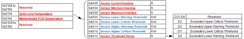
Interrupt Vector and Steering
| Addr (Hex) | Name | Read/Write |
|---|---|---|
| 0x0500 - 0x057C | Module 1 Interrupt Vector 1 - 32 | R/W |
| 0x0600 - 0x067C | Module 1 Interrupt Steering 1 - 32 | R/W |
| 0x0700 - 0x077C | Module 2 Interrupt Vector 1 - 32 | R/W |
| 0x0800 - 0x087C | Module 2 Interrupt Steering 1 - 32 | R/W |
Module Control Command Requests
| Addr (Hex) | Name | Read/Write |
|---|---|---|
| 0x01D8 | Module Slot 1 Command Request | R/W |
| 0x01DC | Module Slot 2 Command Request | R/W |
Module Health Monitoring Registers
Module Communications Status
| Addr (Hex) | Name | Read/Write |
|---|---|---|
| 0x01B8 | Module Slot 1 Communications Status | R |
| 0x01BC | Module Slot 2 Communications Status | R |
Module BIT Status
| Addr (Hex) | Name | Read/Write |
|---|---|---|
| 0x0128 | Module BIT Status (current and latched) | R |
Scratchpad Area
| Addr (Hex) | Name | Read/Write |
|---|---|---|
| 0x3800 - 0x3BFF | Scratchpad Registers | R/W |
Ethernet
(For detailed supplement, please visit the NAI web-site specific product page and refer to: Ethernet Interface for Generation 5 SBC and Embedded IO Boards Specification)
The Ethernet Interface Option allows communications and control access to all function modules either via the system BUS or Ethernet ports 1 or 2.
| Ethernet 1 | Ethernet 2 | |
|---|---|---|
| The default IP address: | 192.168.1.16 | 192.168.2.16 |
| The default subnet: | 255.255.255.0 | 255.255.255.0 |
| The default gateway: | 192.168.1.1 | 192.168.2.1 |
Note
Actual “as shipped” card Ethernet default IP addresses may vary based upon final ATP configuration(s).) Ethernet Port IP addresses may be field re-flashed to new default programmed addressed via use of the “IP Configuring for Ethernet Supported Boards” FLASH software support kit, available/documented from the specific product web page.
The NAI interface supports IPv4 and IPv6 and both the TCP and UDP protocols. The Ethernet Operation Mode Command Listener application running on the motherboard host processor implements the operation interface. The listener is operational on startup through the nai_MBStartup process and listen on specific ports for commands to process. The default ports are listed below:
- TCP1 - Port 52801
- TCP2 - Port 52802
- UDP1 - Port 52801
- UDP2 - Port 52802
Ethernet Message Framework
The interface uses a specific message framework for all commands and responses. All messages begin with a Preamble code and end with a Postamble code. The message framework is shown below.
| Preamble 2 bytes Always 0xD30F |
|---|
| SequenceNo 2 bytes |
| Type Code 2 byte |
| Message Length (2 bytes) |
| Payload (0..1414 bytes) |
| Postamble 2 bytes Always 0xF03D |
Message Elements
| Preamble | The Preamble is used to delineate the beginning of a message frame. The Preamble is always 0xD30F. |
|---|---|
| SequenceNo | The SequenceNo is used to associate Commands with Responses. |
| Type Code | Type Codes are used to define the type of Command or Response the message contains. |
| Message Length | The Message Length is the number of bytes in the complete message frame starting with and including the Preamble and ending with and including the Postamble. |
| Payload | The Payload contains the unique data that makes up the command or response. Payloads vary based on command type. |
| Postamble | The Postamble is use to delineate the end of a message frame. The Postamble is always 0xF03D. |
Notes
- The messaging protocol applies only to card products.
- Messaging is managed by the connected (client) computer. The client computer will send a single message and wait for a reply from the card. Multiple cards may be managed from a single computer, subject to channel and computer capacity.
Board Addressing
The interface provides two main addressing areas: Onboard and Off-board.
Onboard addressing refers to accessing resources located on the board that is implementing the operation interface (including its modules).
Off-board addressing refers to accessing resources located on another board reachable via VME, PCI, or other bus. Off-board addressing requires a Master/Slave configuration.
The user must always specify if a particular address is Onboard or Off-board. See the command descriptions for the onboard and off-board flags.
Within a particular board (Onboard or Off-board), the address space is broken up into two areas: Motherboard Common Address Space and Module Address Space. All addresses are 32-bit.
Motherboard Common Address Space starts at 0x00000000 and ends at 0x00004000. This is a 4Kx32-bit address space (16 kbytes).
Module Address Space starts at 0x00004000. Module addressing is dynamically configured at startup. NAI boards support between 1 and 6 modules. The minimum module address space size is 4Kx32 (16 kbytes) and module sizes are always a multiple of 4Kx32.
Module addressing is dynamic and cumulative. The first detected module (starting with Slot 1) is given an address of 0x00004000. The 2nd detected Module is given an address of:
First_Detected_Module_Address + First_Detected_Module_Size
Note
Slots do not define addresses.
If no module is detected in a module slot, that slot is not given an address. Therefore, if the first detected Module is in Slot 2, then that module address will be 0x00004000. If the next detected module is in Slot 4, then the address of that Module will be:
Second_Detected_Module_Address = First_Detected_Module_Address + First_Detected_Module_Size
If a 3rd Module is detected in Slot 6, then the address of that Module will be:
Third_Detected_Module_Address = Second_Detected_Module_Address + Second_Detected_Module_Size
Note
Module addresses are calculated at each board startup when the modules are detected. Therefore, if a module should fail to be detected due to malfunction or because it was removed from the motherboard, the addresses of the modules that follow it in the slot sequence will be altered. This is important to note when programming to this interface.
Users can always retrieve the Module Addresses, Module Sizes and Module IDs from the fixed Motherboard Common address area. This data is set upon each board startup. While the Module Addressing is dynamic, the address where these addresses are stored is fixed. For example, to find the startup address of the module location in Slot 3, refer to the MB Common Address 0x00000408 from the Motherboard Common Addresses table that follows.
Ethernet Wiring Convention
| RJ-45 Pin | T568A Color | T568B Color | 10/100Base-T | 1000BASE-T | NAI wiring convention |
|---|---|---|---|---|---|
| 1 | white/green stripe | white/orange stripe | TX+ | DA+ | ETH-TP0+ |
| 2 | green | orange | TX- | DA- | ETH-TP0- |
| 3 | white/orange stripe | white/green stripe | RX+ | DB+ | ETH-TP1+ |
| 4 | blue | blue | DC+ | ETH-TP2+ | |
| 5 | white/blue stripe | white/blue stripe | DC- | ETH-TP2- | |
| 6 | orange | green | RX- | DB- | ETH-TP1- |
| 7 | white/brown stripe | white/brown stripe | DD+ | ETH-TP3+ | |
| 8 | brown | brown | DD- | ETH-TP3- |
Synchro/Resolver and LVDT/RVDT Simulation Module Code Tables
Select the Digital-to-Synchro (DSx), Digital-to-Resolver (DRx) or Digital-to-LVDT/RVDT (DLx) module ID corresponding to the application operating parameters required from the following code table (where x = the specific module ID designator). Customer should indicate the actual frequency applicable the design to assure that the correct default band width is set at the factory. All Input and Reference voltages are auto ranging. Frequency/voltage band tolerances +/- 10%. For availability and ranges other than those listed contact the factory. Specifications may be subject to change.
- Single Channel module pending availability (contact factory)
| Module ID | Format | Channel(s) | Output Voltage VL-L (Vrms) | Reference Voltage (Vrms) | Frequency Range (Hz) | Power / CH maximum (VA) | Notes |
| DS1 | SYN | 1* | 2 - 28 | 2 - 115 | 47 - 1 K | 3 | |
| DR1 | RSL | ||||||
| DL1 | LVDT/RVDT | ||||||
| DS2 | SYN | 1* | 2 - 28 | 2 - 115 | 1 K - 5 K | 3 | |
| DR2 | RSL | ||||||
| DL2 | LVDT/RVDT | ||||||
| DS3 | SYN | 1* | 2 - 28 | 2 - 115 | 5 K - 10 K | 3 | |
| DR3 | RSL | ||||||
| DL3 | LVDT/RVDT | ||||||
| DS4 | SYN | 1* | 2 - 28 | 2 - 115 | 10 K - 20 K | 3 | |
| DR4 | RSL | ||||||
| DL4 | LVDT/RVDT | ||||||
| DS5 | SYN | 1* | 28 - 90 | 2 - 115 | 47 - 1 K | 3 | |
| DR5 | RSL | ||||||
| DL5 | LVDT/RVDT | ||||||
| DSX | SYN | 1* | X | X | X | X | X = TBD; special configuration, requires special part number code designation, contact factory |
| DRX | RSL | ||||||
| DLX | LVDT/RVDT | ||||||
| DSA | SYN | 2 | 2 - 28 | 2 - 115 | 47 - 1 K | 1.5 | |
| DRA | RSL | ||||||
| DLA | LVDT/RVDT | ||||||
| DSB | SYN | 2 | 2 - 28 | 2 - 115 | 1 K - 5 K | 1.5 | |
| DRB | RSL | ||||||
| DLB | LVDT/RVDT | ||||||
| DSC | SYN | 2 | 2 - 28 | 2 - 115 | 5 K - 10 K | 1.5 | |
| DRC | RSL | ||||||
| DLC | LVDT/RVDT | ||||||
| DSD | SYN | 2 | 2 - 28 | 2 - 115 | 10 K - 20 K | 1.5 | |
| DRD | RSL | ||||||
| DLD | LVDT/RVDT | ||||||
| DSE | SYN | 2 | 28 - 90 | 2 - 115 | 47 - 1 K | 2.2 | |
| DRE | RSL | ||||||
| DLE | LVDT/RVDT | ||||||
| DSY | SYN | 2 | Y | Y | Y | Y | Y = TBD; special configuration, requires special part number code designation, contact factory |
| DRY | RSL | ||||||
| DLY | LVDT/RVDT | ||||||
| DSJ | SYN | 3 | 2 - 28 | 2 - 115 | 47 - 1 K | 0.5 | |
| DRJ | RSL | ||||||
| DLJ | LVDT/RVDT | ||||||
| DSK | SYN | 3 | 2 - 28 | 2 - 115 | 1 K - 5 K | 0.5 | |
| DRK | RSL | ||||||
| DLK | LVDT/RVDT | ||||||
| DSL | SYN | 3 | 2 - 28 | 2 - 115 | 5 K - 10 K | 0.5 | |
| DRL | RSL | ||||||
| DLL | LVDT/RVDT | ||||||
| DSM | SYN | 3 | 2 - 28 | 2 - 115 | 10 K - 20 K | 0.5 | |
| DRM | RSL | ||||||
| DLM | LVDT/RVDT | ||||||
| DSN | SYN | 3 | 28 - 90 | 2 - 115 | 47 - 1 K | 0.5 | |
| DRN | RSL | ||||||
| DLN | LVDT/RVDT | ||||||
| DSZ | SYN | 3 | Z | Z | Z | Z | Z = TBD; special configuration, requires special part number code designation, contact factory |
| DRZ | RSL | ||||||
| DLZ | LVDT/RVDT |
Synchro/Resolver and LVDT/RVDT Measurement Module Code Tables
SYN/RSL Four-Channel Measurement (Field Programmable SYN/RSL)
Select the Synchro/Resolver-to-Digital (SDx) module ID corresponding to the application operating parameters required from the following code table (where x = the specific module ID designator). Customer should indicate the actual frequency applicable to the design to assure that the correct default band width is set at the factory. All Input and Reference voltages are auto ranging. For availability and ranges other than those listed contact the factory. Specifications may be subject to change.
Frequency/voltage band tolerances +/- 10%.
| Module ID | Input Voltage V (Vrms) | Reference Voltage (Vrms) | Frequency Range (Hz) | Notes |
|---|---|---|---|---|
| SD1 | 2 - 28 | 2 - 115 | 47 - 1 K | |
| SD2 | 2 - 28 | 2 - 115 | 1K - 5 K | |
| SD3 | 2 - 28 | 2 - 115 | 5K - 10 K | |
| SD4* | 2 - 28 | 2 - 115 | 10K - 20 K | |
| SD5 | 28 - 90 | 2 - 115 | 47 - 1 K | |
| SDX* | X | X | X | X = TBD; special configuration, requires special part number code designation, contact factory |
*Consult factory for availability
LVDT/RVDT Four-Channel Measurement (Field Programmable 2, 3 or 4-Wire)
Select the LVDT/RVDT-to-Digital (LDx) module ID corresponding to the application operating parameters required from the following code table (where x = the specific module ID designator). Customer should indicate the actual frequency applicable to the design to assure that the correct default band width is set at the factory. All Input and Excitation voltages are auto ranging. For availability and ranges other than those listed contact the factory. Specifications may be subject to change.
Frequency/voltage band tolerances +/- 10%.
| Module ID | Input Signal Voltage V (Vrms) | Excitation Voltage (Vrms) | Frequency Range (Hz) | Notes |
|---|---|---|---|---|
| LD1 | 2 - 28 | 2 - 115 | 47 - 1 K | |
| LD2 | 2 - 28 | 2 - 115 | 1K - 5 K | |
| LD3 | 2 - 28 | 2 - 115 | 5K - 10 K | |
| LD4* | 2 - 28 | 2 - 115 | 10K - 20 K | |
| LD5 | 28 - 90 | 2 - 115 | 47 - 1 K | |
| LDX* | X | X | X | X = TBD; special configuration, requires special part number code designation, contact factory |
*Consult factory for availability
REVISION HISTORY
| Motherboard Manual - 68INT6 Revision History | |||
| Revision | Revision Date | Description | C |
| 2023-09-28 | ECO C10783, initial release of 68INT6 manual. | C1 | 2023-11-29 |
| ECO C11009, pg.5, update block diagram (SDRAM now 'Up to 64 GB'). Pg.5, update SDRAM features bullet (SDRAM now 'Up to 64 GB'). Pg.9, update SDRAM bullet (SDRAM now 'Up to 64GB'). Pg.13, update SDRAM bullet (SDRAM now 'Up to 64 GB'; new SDRAM part numbers). Pg.31, added SDRAM option code 6 (64 GB). | C2 | 2024-01-09 | ECO C11116, pg.1, changed 'i7-1186GRE' to 'i7-118xGRE Certifiable'. Pg.5, changed 'i7- 1186GRE' to 'i7-118xGRE Certifiable'; updated Intel Core part number in block diagram. Pg.5, revised product description. Pg.5, added processor type delivery options bullet. Pg.8, changed 'i7- 1186GRE' bullet references to 'i7-118xGRE Certifiable'. Pg.9, added NOTE to processor bullet. Pg.13, changed 'i7-1186GRE' to 'i7-118xGRE' in DDR4 SDRAM. Pg.14, changed 'i7-1186GRE' to 'i7-118xGRE' in Video. Pg.31, changed Intel Core processor option code '0' from 'Reserved' to 'Intel Core i7-1185GRE'; changed option code '1' from '(Default)' to '(Certifiable)'. Pg.37, changed 'i7-1186GRE' to 'i7-118xGRE'. Pg.39, changed 'i7-1186GRE' to 'i7-118xGRE' |
| C3 | 2024-04-04 | ECO C11364, pg.28, updated sub-section heading to clarify that table refers to 'standard' XMC only; changed 'J16' to 'J15' in 'XMC' column. Pg.31, added Note 6 & option codes '2' & '3' to HS Fabric Lanes option. Pg.31, deprecated SDRAM option code '4'; option code '5' now default. Pg.31, added (default) to Profile I/O option code '2'. Pg.31, added Note 6 to Notes table. | C4 |
| 2024-04-10 | ECO C11403, pg.31, corrected default HS Fabric Lanes option code (from '0' to '1'). | C5 | 2024-05-16 |
| ECO C11538, pg.22, added XMC-only power designations to Rear I/O Summary. Pg.23, added XMC references and Note for pins that require them for non-NAI XMC functionality. Pg.24/26, changed XMCJ15 to XMCJ16 in pinout tables. Pg.28, changed pin F3 from GND to +12V-XMC. Removed Zynq Core/Aux/DDR Voltage register descriptions from Motherboard Monitoring | Registers section. Pg.43, updated MB Sensor Summary Status register to add PS references; updated Bit table to change voltage/current bits to 'reserved'. Pg.43, updated MB/PS Sensor Registers description to better describe register functionality and to add figure. Pg.44, added 'Exceeded' to threshold bit descriptions. Pg.44-45, removed voltage/current references from sensor descriptions. Pg.49, removed offset 0x0124 (not required). Pg.49, removed Zynq Core/Aux/DDR Voltage register offsets. Pg.50, updated MB Health Monitoring Registers offset tables. | ||
DOCS.NAII REVISIONS
| Revision Date | Description |
|---|---|
| 2024-11-25 | Added ‘Operating Frequency’ subsection to ‘Initial Setup’ section. |
| 2025-01-29 | Updated 68INT6 power spec in overview section (from 30W to 55W); updated 68INT6 power spec in general MB specs table (from 2.5A to 4.6A). |
| 2025-02-12 | Added username/password for Ubuntu. |
| 2025-06-02 | Updated 68INT6 Standard XMC pinout table to remove row 20 (not applicable to non-NAI XMC boards). |
| 2025-06-26 | Added pinout details for RS-232 and RS-422/485 configurations on P2 IO plane. |
| 2025-10-23 | Updated formatting of 68INT6 pinout tables for quality; added audio pinouts/details/note to P2 pinout table for 68INT6-A/-B/-C configurations; updated 68INT6 VITA 61/42 XMC pinout table; removed Device ID#. |
| 2025-10-28 | In P2 pinout table, changed PORTB-R(L) to HEADPHONE-R(L); changed PORTA-R(L) to MIC; changed SENSE-A to GND; updated audio option description for clarity. updated audio option table to clarify which P2 row/wafers use audio option signals & which MOD2 IO pins are being replaced; added Pin 27 Note. |
NAI Cares
North Atlantic Industries (NAI) is a leading independent supplier of Embedded I/O Boards, Single Board Computers, Rugged Power Supplies, Embedded Systems and Motion Simulation and Measurement Instruments for the Military, Aerospace and Industrial Industries. We accelerate our clients’ time-to-mission with a unique approach based on a Configurable Open Systems Architecture™ (COSA®) that delivers the best of both worlds: custom solutions from standard COTS components.
We have built a reputation by listening to our customers, understanding their needs, and designing, testing and delivering board and system-level products for their most demanding air, land and sea requirements. If you have any applications or questions regarding the use of our products, please contact us for an expedient solution.
Please visit us at: www.naii.com or select one of the following for immediate assistance:
Documentation
FAQ
Application Notes
http://www.naii.com/applicationnotes
Calibration and Repairs
http://www.naii.com/calibrationrepairs
Call Us
(631) 567-1100
Link to original