64ARM1 DATA SHEET
Click here for the 64ARM1 data sheet.
INTRODUCTION
North Atlantic Industries (NAI) is a leading independent supplier of rugged COTS embedded computing products for industrial, commercial aerospace, and defense markets. Aligned with MOSA, SOSA and FACE standards, NAI’s Configurable Open System Architecture™ (COSA®) accelerates a customer’s time-to-mission by providing the most modular, agile, and rugged COTS portfolio of embedded smart modules, I/O boards, Single Board Computers (SBCs), Power Supplies and Ruggedized Systems of its kind. COSA products are pre-engineered to work together, enabling easy changes, reuses, or repurposing down the road. By utilizing FPGAs and SoCs, NAI has created smart modules that enable the rapid creation of configurable mission systems while reducing or eliminating SBC overhead.
NAI’s 64ARM1 6U VME Single Board Computer (SBC) is a rugged processing board which provides low power, cost-sensitive processing capabilities designed for demanding aerospace, defense, and industrial applications. When combined with NAI’s smart modules, the board’s modular I/O approach makes it a highly flexible and integrable solution for demanding computing environments.
64ARM1 Overview
The 64ARM1 6U VME Single Board Computer (SBC) offers a variety of features designed to meet the needs of complex requirements for integrated multifunction I/O-intensive, mission-critical applications. Some of the key features include:
6U VME SBC: The 64ARM1 is housed in a 6U VME form factor, delivering exceptional levels of performance and power efficiency with all the functionality required in rugged, embedded SWaP-optimized defense and aerospace programs.
Connection Flexibility: The SBC provides flexibility in connectivity options, with the ability to connect to devices via the front panel, rear panel, or both. This feature is particularly useful in different mounting or space-constrained scenarios.
2x 10/100/1000 Base-T Ethernet: The 64ARM1 has two 10/100/1000 Base-T Ethernet ports, with the option to have one to the rear, one to the front I/O, or both to the rear.
ARM® Cortex®-A9 Dual Core 800 MHz Processor: The 64ARM1 offers a significant advantage by providing enhanced processing power and efficiency. With its dual-core configuration and 800 MHz clock speed, it enables advanced computational tasks and real-time processing capabilities, making it an ideal choice for applications requiring high performance computing within a compact form factor.
512 MB DDR3L SDRAM: The SBC features a 512 MB DDR3L SDRAM, which offers users a dependable memory solution for demanding military, industrial, and aerospace environments:
-
The low voltage (‘L’) operation reduces power consumption, crucial for systems where power efficiency is essential for extended mission and battery operated devices.
-
DDR3L SDRAM ensures data integrity even in harsh conditions, and can be ruggedized to withstand extreme temperatures, shocks, and vibrations in challenging environments..
-
DDR3L SDRAM provides long-term support, making them ideal for equipment that needs to be in service for extended periods of time.
32 GB SATA II NAND Flash: The 64ARM1 utilizes a SATA II NAND Flash memory capable of providing up to 32 GB of storage, offering high-capacity, durable, reliable, and rugged data storage. It is well suited for applications where data must be securely stored and accessed in challenging environmental conditions while providing a cost-effective storage solution.
Less than 8 Watts Motherboard Power Dissipation: With a power dissipation of less than 8 watts, the 64ARM1 proves a highly efficient solution, offering superior energy conservation, effective thermal management, extended mission endurance, and heightened reliability for demanding military, industrial, and aerospace applications.
Support for six independent, smart function:
The SBC can support up to six independent, smart function modules based on the COSA® architecture. With over 100 modules to choose from, this allows for a wide range of input and output capabilities, including analog and digital I/O, signal generation and acquisition, and communication interfaces. Each function module slot has an independent x1 SerDes interface for motherboard-to-smart module interface, to offload the host processor from I/O management.
- The 64ARM1’s function slot #6 features the capability to utilize either a PCIe interface that enables up to 2 additional Gig-E ports or an independent external SATA II interface that supports a 256 GB memory expansion over the VME backplane. These interfaces facilitate the expansion of external host SBC functions, which enables engineers and system architects to easily configure the board with the necessary modules and accelerate SWaP-optimized system deployment.
Peripheral I/O:
The 64ARM1 board features several sophisticated on-board (on motherboard) peripheral I/O interfaces, all of which are rear accessed. Designed to meet the diverse requirements of complex projects, this comprehensive I/O suite includes:
-
A single USB 2.0 interface to front maintenance J7, enabling users to transfer data quickly and reliably.
-
An I2C port provides a versatile serial communication interface for controlling, monitoring, and interacting with devices located at the rear of the chassis. It consists of two wires (clock and data) and allows for bidirectional communication.
-
An RS-232 console/maintenance port (front and rear) that provides a standard interface for communicating with the board for maintenance and debugging purposes. This serial port can be used for configuring the board or accessing diagnostic information and logs.
Background Built-In-Test (BIT):
The 64ARM1 board continually checks and reports on the health of each channel, allowing for proactive maintenance and reducing the likelihood of downtime.
Software Support Kits (SSKs):
SSKs are provided ‘free of charge’ and include base motherboard and function module API libraries and documentation. Sample and source code are also available, as well as support for real-time operating systems (RTOS) such as Wind River® VxWorks®, and Xilinx® PetaLinux, providing developers with flexibility and customization options for their specific application needs.
VICTORY Interface Services:
NAI offers VICTORY Interface Services as an option, providing an open industry-standard approach for integrating different components in a system.
Commercial and rugged mechanical options:
The 64ARM1 is available in both commercial and rugged models, making it suitable for a wide range of applications.
-
Operating temperature: The board has a wide operating temperature range, with models operating from:
-
0° C to 70° C (commercial model)
-
-40° C to +85° C (rugged model)
-
SOFTWARE SUPPORT
The ENAIBL Software Support Kit (SSK) is supplied with all system platform based board level products. This platform’s SSK contents include html format help documentation which defines board specific library functions and their respective parameter requirements. A board specific library and its source code is provided (module level ‘C’ and header files) to facilitate function implementation independent of user operating system (O/S). Portability files are provided to identify Board Support Package (BSP) dependent functions and help port code to other common system BSPs. With the use of the provided help documentation, these libraries are easily ported to any 32-bit O/S such as RTOS or Linux.
The latest version of a board specific SSK can be downloaded from our website www.naii.com in the software downloads section. A Quick-Start Software Manual is also available for download where the SSK contents are detailed, Quick-Start Instructions provided and GUI applications are described therein. For other operating system support, contact factory.
Link to original
SPECIFICATIONS
General for the Motherboard
| VME Data Transfer: | Data transfer within 200 ns |
| Interrupts: | One Interrupt capability is implemented. One of seven priority lines can be specified. |
| Power (Motherboard): | +5 VDC @ 1.6 A (typical) Then add power for each individual module |
| Temperature, Operating: | "C" =0° C to +70° C, "H" =-40° C to +85° C (see part number) |
| Storage Temperature: | -55° C to +105° C |
| Temperature Cycling: | Each board is cycled from -40° C to +85° C for option “H” |
| Size | |
| Height: | 9.2" / 233.4 mm (6U) |
| Width: | 0.8” / 20.3 mm (4HP) |
| Depth: | 6.3“ / 160 mm deep |
| Weight: | 18 oz. (544 g) unpopulated, then add weight for each module (see module spec) add 4 oz. (114 g) for wedgelocks (conduction cooled option) |
Specifications are subject to change without notice.
Environmental
Unless otherwise specified, the following table outlines the general Environmental Specifications design guidelines for board level products of North Atlantic Industries. All our cPCI, VME and OpenVPX boards are designed for either air or conduction cooling. All boards also incorporate appropriate stiffening to ensure performance during shock and vibration but also to assure reliable operation (lower fatigue stresses) over the service life of the product.
| Parameters | Level | ||
| 1 / Commercial-AC (Air Cooled) | 2 / Rugged-AC (Air Cooled) | 3 / Rugged-CC (Conduction Cooled) | |
| Temperature - Operating | 0° C to 70° C, AmbientH | -40° C to 85° C, AmbientI | -40° C to 85° C, at wedge lock thermal interface |
| Temperature - Storage | -40° C to 85° C | -55° C to 105° C | -55° C to 105° C |
| Humidity - Operating | 0 to 95%, non-condensing | 0 to 95%, non-condensing | 0 to 95%, non-condensing |
| Humidity - Storage | 0 to 95%, non-condensing | 0 to 95%, non-condensing | 0 to 95%, non-condensing |
| Vibration - SineA | 2 g peak, 15 Hz - 2 kHzB | 6 g peak, 15 Hz - 2 kHzB | 10 g peak, 15 Hz - 2 kHzC |
| Vibration - RandomD | .002 g2 /Hz, 15 Hz - 2 kHz | 0.04 g2 /Hz, 15 Hz - 2 kHz | 0.1 g2 /Hz, 15 Hz - 2 kHzE |
| ShockF | 20 g peak, half-sine, 11 ms | 30 g peak, half-sine 11 ms | 40 g peak, half-sine, 11 ms |
| Low PressureG | Up to 15,000 ft. | Up to 50,000 ft. | Up to 50,000 ft. |
Notes:
A. Based on sweep duration of ten minutes per axis on each of the three mutually perpendicular axes. B. Displacement limited to 0.10 D.A. from 15 to 44 Hz. C. Displacement limited to 0.436 D.A. from 15 to 21 Hz. D. 60 minutes per axis on each of the three mutually perpendicular axes. E. Per MIL-STD-810G, Method 5.14.6 Procedure I, Fig.514.6C-6 Category 7 tailored (11.65 Grms): 15 Hz - 2 kHz; ASD (PSD) at 0.04 g2/Hz between 15 Hz - 150 Hz, increasing @ 4 dB/octave from 0.04 g2/Hz to 0.1 g /Hz between 150 Hz - 300 Hz, 0.1 g2/Hz between 300 Hz - 1000 Hz, decreasing @ 6 dB/octave from 0.1 g2/Hz to 0.025 g2/Hz between 1000 Hz - 2000 Hz. Three hits per direction per axis (total of 18 hits). F. Three hits per direction per axis (total of 18 hits). G. For altitudes higher than 50,000 ft., contact NAI. H. High temperature operation requires 350 lfm minimum air flow across cover/heatsink (module dependent). I. High temperature operation requires 600 lfm minimum air flow across cover/heatsink (module dependent).
Specifications subject to change without notice
REGISTER MEMORY MAP ADDRESSING
The register map address consists of the following:
• cPCI/PCIe BAR or Base Address for the Board • Module Slot Base Address • Function Offset Address
Board Base Address
The table below lists the BAR used for access to the motherboard and module registers. The second BAR is used internally for motherboard and module firmware updates. The other cPCI/PCIe BARs not listed are not used.
| NAI Boards | Device ID | Bus | Motherboard and Module Register Access | Motherboard and Module Firmware Updates |
| Controller/Master Board | ||||
| 64ARM1 | N/A | VME | Slave Window 1 Size: 8M Bytes | Slave Window 2 Size: 8M Bytes |
Module Slot and Function Addresses
The memory map for the modules are dependent on the types of modules on the board and the order in which the modules are installed on the board as well as the firmware installed on the motherboard. The function modules are enumerated allowing for dynamic memory space allocation and therefore the “start” address of the module function register area is factory pre-defined (and read from) the Module Address register. Refer to Figure 1 for an example.
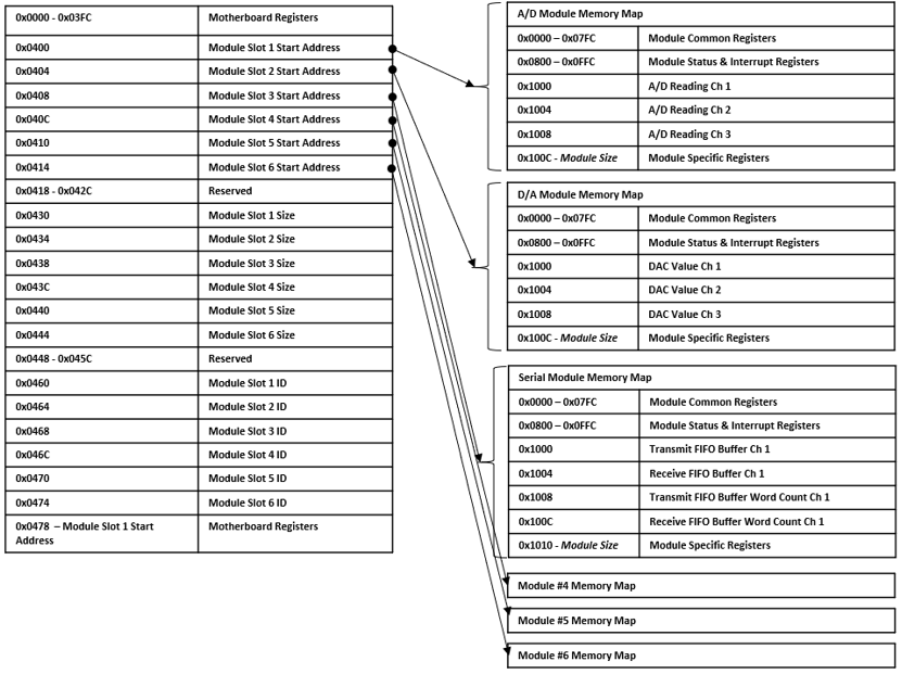
Figure 1. Register Memory Map Addressing for Motherboards with 6 Modules
Address Calculation
Motherboard Registers
Read/Write access to the motherboard registers starts with the base address for the board and then the motherboard base offset address.
For example, to address Module Slot 1 Start Address register (i.e. register address = 0x0400):
- Start with the base address for the board.
- Add the motherboard register address offset.
| Motherboard Address = | Base Address Motherboard Address Offset | = 0x0000 0400 |
| 0x0000 0000 + 0x0400 |
Module Registers:
Read/Write access to the Function module’s registers start with the base address of the board. Add the “content” for the Module Start Address and then, add the specific module function register offset.
For example, to address an appropriate/specific function module with a register offset:
- Start with the base address for the board.
- Add the value (contents) from the module base address offset register (contents/value of Motherboard Memory register for Module 1 (i.e., @ 0x0400) = 0x4000.
- Then add the specific module function Register Offset of interest (i.e., A/D Reading Ch 1 @ 0x1000)
| (Function Specific) Address = | Base Address + | Module Base Address Offset + | Function Register Offset | = 0x0000 5000 |
| 0x0000 0000 | 0x4000 | 0x1000 |
REGISTER DESCRIPTIONS
Module Information Registers
The Module Slot Addressing Ready, Module Slot Address, Module Slot Size, and Module Slot ID registers provide information about the modules detected on the board.
Module Slot Addressing Ready
Link to original
Function: Indicates that the module slots are ready to be addressed. Type: unsigned binary word (32-bit) Data Range: 0x0000 0000 to 0xFFFF FFFF Read/Write: R Initialized Value: 0xA5A5A5A5 Operational Settings: This register will contain the value of 0xA5A5A5A5 when the module addresses have been determined.
Link to original
Module Slot Address Function: Specifies the Base Address for the module in the specific slot position. Type: unsigned binary word (32-bit) Data Range: 0x0000 0000 to 0xFFFF FFFF Read/Write: R Initialized Value: Based on board's module configuration. Operational Settings: 0x0000 0000 indicates no Module found.
Link to original
Module Slot Size Function: Specifies the Memory Size (in bytes) allocated for the module in the specific slot position. Type: unsigned binary word (32-bit) Range: 0x0000 0000 to 0xFFFF FFFF Read/Write: R Initialized Value: Assigned by factory for the module. Operational Settings: 0x0000 0000 indicates no Module found.
Module Slot ID Function: Specifies the Model ID for the module in the specified slot position. Type: 4-character ASCII string Data Range: 0x0000 0000 to 0xFFFF FFFF Read/Write: R Initialized Value: Assigned by factory for the module. Operational Settings: The Module ID is formatted as four ASCII bytes: three characters followed by a space. Module IDs are in little-endian order with a single space following the first three characters. For example, 'TL1' is '1LT', 'SC1' is '1CS' and so forth. Example below is for “TL1” (MSB justified). All value of 0000 0000 indicates no Module found. Link to original
D31 D30 D29 D28 D27 D26 D25 D24 D23 D22 D21 D20 D19 D18 D17 D16 ASCII Character (ex: 'T' - 0x54) ASCII Character (ex: 'L' - 0x4C) D15 D14 D13 D12 D11 D10 D9 D8 D7 D6 D5 D4 D3 D2 D1 D0 ASCII Character (ex: '1' - 0x31) ASCII Space (' ' - 0x20)
Hardware Information Registers
The registers identified in this section provide information about the board’s hardware.
Link to original
Product Serial Number Function: Specifies the Board Serial Number. Type: unsigned binary word (32-bit) Data Range: 0x0000 0000 to 0xFFFF FFFF Read/Write: R Initialized Value: Serial number assigned by factory for the board. Operational Settings: N/A
Platform
Function: Specifies the Board Platform Identifier. Values are for the ASCII characters for the NAI valid platforms (Identifiers).
Type: unsigned binary word (32-bit)
Data Range: See table below.
Read/Write: R
Initialized Value: ASCII code is for the Platform Identifier of the board
Operational Settings: Valid NAI platform and the associated value for the platform is shown below:
| NAI Platform | Platform Identifier | ASCII Binary Values (Note: little-endian order of ascii values) |
|---|---|---|
| 6U VME | 64 | 0x0000 3436 |
Model
Function: Specifies the Board Model Identifier. Value is for the ASCII characters for the NAI valid model.
Type: unsigned binary word (32-bit)
Data Range: See table below.
Read/Write: R
Initialized Value: ASCII code is for the Model Identifier of the board
Operational Settings: Example of NAI model and the associated value for the model is shown below:
| NAI Model | ASCII Binary Values (Note: little-endian order of ascii values) |
|---|---|
| ARM | 0x004D 5241 |
Generation
Function: Specifies the Board Generation. Identifier values are for the ASCII characters for the NAI valid generation identifiers.
Type: unsigned binary word (32-bit)
Data Range: See table below.
Read/Write: R
Initialized Value: ASCII code is for the Generation Identifier of the board
Operational Settings: Example of NAI generation and the associated value for the generation is shown below:
| NAI Generation | ASCII Binary Values (Note: little-endian order of ascii values) |
|---|---|
| 1 | 0x0000 0031 |
Processor Count/Ethernet Count
Function: Specifies the Processor Count and Ethernet Count
Type: unsigned binary word (32-bit)
Data Range: See table below.
Read/Write: R
Operational Settings:
Processor Count - Integer: indicates the number of unique processor types on the motherboard.
| NAI Board | Processor Count | Description | |
| VME | 64ARM1 | 1 | Xilinx Zynq 7015 with Dual Core Cortex A9 |
Ethernet Interface Count - Indicates the number of Ethernet interfaces on the product motherboard. For example, Single Ethernet = 1; Dual
Ethernet = 2.
Processor/Ethernet Interface Count
| D31 | D30 | D29 | D28 | D27 | D26 | D25 | D24 | D23 | D22 | D21 | D20 | D19 | D18 | D17 | D16 |
| Processor Count (See Table) | |||||||||||||||
| D15 | D14 | D13 | D12 | D11 | D10 | D9 | D8 | D7 | D6 | D5 | D4 | D3 | D2 | D1 | D0 |
| Ethernet Count (Based on Part Number Ethernet Options) | |||||||||||||||
Maximum Module Slot Count/ARM Platform Type
Function: Specifies the Maximum Module Slot Count and ARM Platform Type.
Type: unsigned binary word (32-bit)
Data Range: See table below.
Read/Write: R
Operational Settings:
Maximum Module Slot Count - Indicates the number of modules that can be installed on the product.
ARM Platform - Altera = 1; Xilinx X1 = 2; Xilinx X2 = 3; UltraScale = 4
| NAI Board | Maximum Module Slot Count | ARM Platform Type | |
| VME | 64ARM1 | 3 | Xilinx X1 = 2; Xilinx X2 = 3 |
Maximum Module Slot Count / ARM Platform Type
| D31 | D30 | D29 | D28 | D27 | D26 | D25 | D24 | D23 | D22 | D21 | D20 | D19 | D18 | D17 | D16 |
| Maximum Module Slot Count (See Table) | |||||||||||||||
| D15 | D14 | D13 | D12 | D11 | D10 | D9 | D8 | D7 | D6 | D5 | D4 | D3 | D2 | D1 | D0 |
| ARM Platform Type (See Table) | |||||||||||||||
Motherboard Firmware Information Registers
The registers in this section provide information on the revision of the firmware installed on the motherboard.
Motherboard Core (MBCore) Firmware Version Function: Specifies the Version of the NAI factory provided Motherboard Core Application installed on the board. Type: Two (2) unsigned binary word (32-bit) Data Range: 0x0000 0000 to 0xFFFF FFFF Read/Write: R Operational Settings: The motherboard firmware version consists of four components: Major, Minor, Minor 2 and Minor 3. Link to original
Motherboard Core Firmware Version (Note: little-endian order in register) (ex. 4.7.0.0) Word 1 (Ex. 0007 0004 = 4.7 (Major.Minor) D31 D30 D29 D28 D27 D26 D25 D24 D23 D22 D21 D20 D19 D18 D17 D16 Minor (ex: 0x0007 = 7) D15 D14 D13 D12 D11 D10 D9 D8 D7 D6 D5 D4 D3 D2 D1 D0 Major (ex: 0x0004 = 4) Word 2 (Ex. 0x0000 0000 = 0000 = 0.0 (Minor2.Minor3)) D31 D30 D29 D28 D27 D26 D25 D24 D23 D22 D21 D20 D19 D18 D17 D16 Minor 3 (ex: 0x000 = 0) D15 D14 D13 D12 D11 D10 D9 D8 D7 D6 D5 D4 D3 D2 D1 D0 Minor 2 (ex: 0x000 = 0)
Motherboard Firmware Build Time/Date Function: Specifies the Build Date/Time of the NAI factory provided Motherboard Core Application installed on the board. Type: Two (2) unsigned binary word (32-bit) Data Range: N/A Read/Write: R Operational Settings: The motherboard firmware time consists of the Build Date and Build Time. NOTE: On some builds the the Date/Time fields are fixed to 0000 0000 to maintain binary consistency across builds. Link to original
Motherboard Firmware Build Time (Note: little-endian order in register) Word 1 - Build Date (ex. 0x030C 07E2 = 2018-12-03) D31 D30 D29 D28 D27 D26 D25 D24 D23 D22 D21 D20 D19 D18 D17 D16 Day (ex: 0x03 = 3) Month (ex: 0x0C = 12) D15 D14 D13 D12 D11 D10 D9 D8 D7 D6 D5 D4 D3 D2 D1 D0 Year (ex: 0x07E2 = 2018) Word 2 - Build Time (ex. 0x001B 3B0A = 10:59:27) D31 D30 D29 D28 D27 D26 D25 D24 D23 D22 D21 D20 D19 D18 D17 D16 null (0x00) Seconds (ex: 0x1B = 27) D15 D14 D13 D12 D11 D10 D9 D8 D7 D6 D5 D4 D3 D2 D1 D0 Minutes (ex: 0x3B = 59) Hours (ex: 0x0A = 10)
Motherboard Monitoring Registers
The registers in this provide motherboard voltage and temperature measurement information, and where applicable the slave processor measurements.
Temperature Readings Register
The temperature registers provide the current, maximum (from power-up) and minimum (from power-up) for the processor and PCB for Zynq processor, and for the Slave processor.
These registers are only available on Xilinx Generation 5 platforms, and are periodically populated by the motherboard core application, which only runs in Petalinux and BareMetal. For other operating systems, refer to the naibrd Software Support Kit (SSK) naibsp_system_Monitor_Temperature_Get() routine to manually retrieve the temperature (NOTE: this feature is typically utilized for development/factory use only; contact the factory for additional details on potential use, if required).
Function: Specifies the Measured Temperatures on Motherboard.
Type: signed byte (8-bits) for each temperature reading - Six (6) 32-bit words
Data Range: 0x0000 0000 to 0xFFFF 0000
Read/Write: R
Initialized Value: Value corresponding to the measured temperatures based on the table below.
Operational Settings: The 8-bit temperature readings are signed bytes. For example, if the following register contains the value 0x6955 0000:
Example:
Word 3 (Max Zynq Temperatures)
D31 D30 D29 D28 D27 D26 D25 D24 D23 D22 D21 D20 D19 D18 D17 D16 Max Zynq Core Temperature Max Zynq PCB Temperature D15 D14 D13 D12 D11 D10 D9 D8 D7 D6 D5 D4 D3 D2 D1 D0 0x00 0x00 The values would represent the following temperatures:
Temperature Measurements Data Bits Value Temperature (Celsius) Max Zynq Core Temperature D31:D24 0x69 +105° Max Zynq PCB Temperature D23:D16 0x55 +85° Temperature Readings
Word 1 (Current Zynq Temperatures)
D31 D30 D29 D28 D27 D26 D25 D24 D23 D22 D21 D20 D19 D18 D17 D16 Zynq Core Temperature Zynq PCB Temperature D15 D14 D13 D12 D11 D10 D9 D8 D7 D6 D5 D4 D3 D2 D1 D0 0x00 0x00 Word 2 (Current Slave Zynq Temperatures)
D31 D30 D29 D28 D27 D26 D25 D24 D23 D22 D21 D20 D19 D18 D17 D16 Slave Zynq Core Temperature Slave Zynq PCB Temperature D15 D14 D13 D12 D11 D10 D9 D8 D7 D6 D5 D4 D3 D2 D1 D0 0x00 0x00 Word 3 (Max Zynq Temperatures)
D31 D30 D29 D28 D27 D26 D25 D24 D23 D22 D21 D20 D19 D18 D17 D16 Max Zynq Core Temp Max Zynq PCB Temp D15 D14 D13 D12 D11 D10 D9 D8 D7 D6 D5 D4 D3 D2 D1 D0 0x00 0x00 Word 4 (Max Slave Zynq Temperatures)
D31 D30 D29 D28 D27 D26 D25 D24 D23 D22 D21 D20 D19 D18 D17 D16 Max Slave Zynq Core Temp Max Slave Zynq PCB Temp D15 D14 D13 D12 D11 D10 D9 D8 D7 D6 D5 D4 D3 D2 D1 D0 0 0 0 0 0 0 0 0 0 0 0 0 0 0 0 0 Word 5 (Min Zynq Temperatures)
D31 D30 D29 D28 D27 D26 D25 D24 D23 D22 D21 D20 D19 D18 D17 D16 Min Zynq Core Temperature Min Zynq PCB Temperature D15 D14 D13 D12 D11 D10 D9 D8 D7 D6 D5 D4 D3 D2 D1 D0 0 0 0 0 0 0 0 0 0 0 0 0 0 0 0 0 Word 6 (Min Slave Zynq Temperatures)
Link to original
D31 D30 D29 D28 D27 D26 D25 D24 D23 D22 D21 D20 D19 D18 D17 D16 Min Slave Zynq Core Temperature Min Slave Zynq PCB Temperature D15 D14 D13 D12 D11 D10 D9 D8 D7 D6 D5 D4 D3 D2 D1 D0 0 0 0 0 0 0 0 0 0 0 0 0 0 0 0 0
Higher Precision Temperature Readings Registers
These registers provide higher precision readings of the current Zynq and PCB temperatures.
Higher Precision Zynq Core Temperature Function: Specifies the Higher Precision Measured Zynq Core temperature on Interface Board. Type: signed word (16-bits) for integer part and unsigned word (16-bits) for fractional part Data Range: 0x0000 0000 to 0xFFFF FFFF Read/Write: R Initialized Value: Measured Zynq Core temperature on Interface Board Operational Settings: The upper 16-bits represent the signed integer part of the temperature and the lower 16-bits represent the fractional part of the temperature with the resolution of 1/1000 of degree Celsius. For example, if the register contains the value 0x002B 0271, this represents Zynq Core Temperature = 43.625° Celsius, and value 0xFFF6 0177 represents -10.375° Celsius. Link to original
D31 D30 D29 D28 D27 D26 D25 D24 D23 D22 D21 D20 D19 D18 D17 D16 Signed Integer Part of Temperature D15 D14 D13 D12 D11 D10 D9 D8 D7 D6 D5 D4 D3 D2 D1 D0 Fractional Part of Temperature
Higher Precision Motherboard PCB Temperature Function: Specifies the Higher Precision Measured Motherboard PCB temperature. Type: signed word (16-bits) for integer part and unsigned word (16-bits) for fractional part Data Range: 0x0000 0000 to 0xFFFF FFFF Read/Write: R Initialized Value: Measured Motherboard PCB temperature Operational Settings: The upper 16-bits represent the signed integer part of the temperature and the lower 16-bits represent the fractional part of the temperature with the resolution of 1/1000 of degree Celsius. For example, if the register contains the value 0x0020 007D, this represents Interface PCB Temperature = 32.125° Celsius, and value 0xFFE8 036B represents -24.875° Celsius. Link to original
D31 D30 D29 D28 D27 D26 D25 D24 D23 D22 D21 D20 D19 D18 D17 D16 Signed Integer Part of Temperature D15 D14 D13 D12 D11 D10 D9 D8 D7 D6 D5 D4 D3 D2 D1 D0 Fractional Part of Temperature
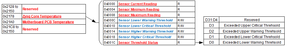
Motherboard Health Monitoring Registers
The registers in this section provide a summary of motherboard temperature sensors and their corresponding bits. Additionally, this section provides an overview of the registers allocated to those sensors, which are used to monitor current/minimum/maximum temperature readings, upper & lower critical/warning temperature thresholds, and whether or not a programmed temperature threshold has been exceeded.
These registers are only available on Xilinx Generation 5 platforms, and are periodically populated by the motherboard core application, which only runs in Petalinux and BareMetal. For other operating systems, refer to the naibrd Software Support Kit (SSK) naibsp_system_Monitor_Temperature_Get() routine to manually retrieve the temperature (NOTE: this feature is typically utilized for development/factory use only; contact the factory for additional details on potential use, if required).
Motherboard Sensor Summary Alarm Function: The corresponding sensor bit is set if the sensor has crossed any of its thresholds. Type: unsigned binary word (32-bits) Data Range: See table below Read/Write: R Initialized Value: 0 Operational Settings: This register provides a summary for motherboard sensors. When the corresponding sensor bit is set, the Sensor Threshold Status register for that sensor will indicate the threshold condition that triggered the event. Link to original
Bit(s) Sensor D31:D5 Reserved D4 Motherboard PCB Temperature D3 Zynq Core Temperature D2:D0 Reserved
Motherboard Sensor Registers
The registers listed in this section apply to each module sensor listed for the Motherboard Sensor Summary Status register. Each individual sensor register provides a group of registers for monitoring motherboard temperatures readings. From these registers, a user can read the current temperature of the sensor in addition to the minimum and maximum temperature readings since power-up. Upper and lower critical/warning temperature thresholds can be set and monitored from these registers. When a programmed temperature threshold is crossed, the Sensor Threshold Status register will set the corresponding bit for that threshold. The figure below shows the functionality of this group of registers when accessing the Zynq Core Temperature sensor as an example.
Link to original
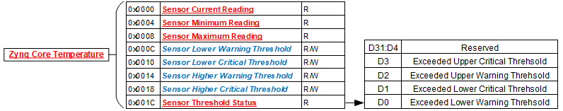
Sensor Threshold Status Function: Reflects which threshold has been crossed Type: unsigned binary word (32-bits) Data Range: See table below Read/Write: R Initialized Value: 0 Operational Settings: The associated bit is set when the sensor reading exceed the corresponding threshold settings. Link to original
Bit(s) Description D31:D4 Reserved D3 Exceeded Upper Critical Threshold D2 Exceeded Upper Warning Threshold D1 Exceeded Lower Critical Threshold D0 Exceeded Lower Warning Threshold
Link to original
Sensor Current Reading Function: Reflects current reading of temperature sensor Type: Single Precision Floating Point Value (IEEE-754) Data Range: Single Precision Floating Point Value (IEEE-754) Read/Write: R Initialized Value: N/A Operational Settings: The register represents current sensor reading as a single precision floating point value. For example, for a temperature sensor, register value 0x41C6 0000 represents temperature = 24.75° Celsius.
Link to original
Sensor Minimum Reading Function: Reflects minimum value of temperature sensor since power up Type: Single Precision Floating Point Value (IEEE-754) Data Range: Single Precision Floating Point Value (IEEE-754) Read/Write: R Initialized Value: N/A Operational Settings: The register represents minimum sensor value as a single precision floating point value. For example, for a temperature sensor, register value 0x41C6 0000 represents temperature = 24.75° Celsius.
Link to original
Sensor Maximum Reading Function: Reflects maximum value of temperature sensor since power up Type: Single Precision Floating Point Value (IEEE-754) Data Range: Single Precision Floating Point Value (IEEE-754) Read/Write: R Initialized Value: N/A Operational Settings: The register represents maximum sensor value as a single precision floating point value. For example, for a temperature sensor, register value 0x41C6 0000 represents temperature = 24.75° Celsius.
Link to original
Sensor Lower Warning Threshold Function: Reflects lower warning threshold of temperature sensor Type: Single Precision Floating Point Value (IEEE-754) Data Range: Single Precision Floating Point Value (IEEE-754) Read/Write: R/W Initialized Value: Default lower warning threshold (value dependent on specific sensor) Operational Settings: The register represents sensor lower warning threshold as a single precision floating point value. For example, for a temperature sensor, register value 0xC220 0000 represents temperature = -40.0° Celsius.
Link to original
Sensor Lower Critical Threshold Function: Reflects lower critical threshold of temperature sensor Type: Single Precision Floating Point Value (IEEE-754) Data Range: Single Precision Floating Point Value (IEEE-754) Read/Write: R/W Initialized Value: Default lower critical threshold (value dependent on specific sensor) Operational Settings: The register represents sensor lower critical threshold as a single precision floating point value. For example, for a temperature sensor, register value 0xC25C 0000 represents temperature = -55.0° Celsius.
Link to original
Sensor Upper Warning Threshold Function: Reflects upper warning threshold of temperature sensor Type: Single Precision Floating Point Value (IEEE-754) Data Range: Single Precision Floating Point Value (IEEE-754) Read/Write: R/W Initialized Value: Default upper warning threshold (value dependent on specific sensor) Operational Settings: The register represents sensor upper warning threshold as a single precision floating point value. For example, for a temperature sensor, register value 0x42AA 0000 represents temperature = 85.0° Celsius.
Link to original
Sensor Upper Critical Threshold Function: Reflects upper critical threshold of temperature sensor Type: Single Precision Floating Point Value (IEEE-754) Data Range: Single Precision Floating Point Value (IEEE-754) Read/Write: R/W Initialized Value: Default upper critical threshold (value dependent on specific sensor) Operational Settings: The register represents sensor upper critical threshold as a single precision floating point value. For example, for a temperature sensor, register value 0x42FA 0000 represents temperature = 125.0° Celsius.
Ethernet Configuration Registers
The registers in this section provide information about the Ethernet Configuration for the two ports on the board.
Important: Regardless if the board is configured for one or two Ethernet ports, the second IP address cannot be on the same Subnet as the First IP Address. The table below provides examples of valid and invalid IP Addresses and Subnet Mask Addresses.
Link to original
First Port (A) IP Address First Port (A) Subnet Mask Second Port (B) IP Address Second Port (B) Subnet Mask Result 192.168.1.5 255.255.255.0 192.168.2.5 255.255.255.0 Good 192.168.1.5 255.255.0.0 192.168.2.5 255.255.0.0 Conflict 192.168.1.5 255.255.0.0 192.168.2.5 255.255.255.0 Conflict 10.0.0.15 255.0.0.0 192.168.1.5 255.255.255.0 Good
Ethernet MAC Address and Ethernet Settings Function: Specifies the Ethernet MAC Address and Ethernet Settings for the Ethernet port. Type: Two (2) unsigned binary word (32-bit) Data Range: See table. Read/Write: R Operational Settings: The Ethernet MAC Address consists of six octets. The Ethernet Settings are defined in table.
Bits Description Values D31:D23 Reserved 0 D22:D21 Duplex 00 = Not Specified, ` 01 = Half Duplex, ` 10 = Full Duplex, + 11 = Reserved D20:D18 Speed 000 = Not Specified, ` 001 = 10 Mbps, ` 010 = 100 Mbps, ` 011 = 1000 Mbps, ` 100 = 2500 Mbps, ` 101 = 10000 Mbps, ` 110 = Reserved, + 111 = Reserved D17 Auto Negotiate 0 = Enabled, + 1 = Disabled D16 Static IP Address 0 = Enabled, + 1 = Disabled Link to original
Ethernet MAC Address and Ethernet Settings (Note: little-endian order in register) Word 1 (Ethernet MAC Address (Octets 1-4)) (ex: aa:bb:cc:dd:ee:ff) D31 D30 D29 D28 D27 D26 D25 D24 D23 D22 D21 D20 D19 D18 D17 D16 MAC Address Octet 4 (ex: 0xDD) MAC Address Octet 3 (ex: 0xCC) D15 D14 D13 D12 D11 D10 D9 D8 D7 D6 D5 D4 D3 D2 D1 D0 MAC Address Octet 2 (ex: 0xBB) MAC Address Octet 1 (ex: 0xAA) Word 2 (Ethernet MAC Address (Octets 5-6) and Ethernet Settings) D31 D30 D29 D28 D27 D26 D25 D24 D23 D22 D21 D20 D19 D18 D17 D16 Ethernet Settings (See table) D15 D14 D13 D12 D11 D10 D9 D8 D7 D6 D5 D4 D3 D2 D1 D0 MAC Address Octet 6 (ex: 0xFF) MAC Address Octet 5 (ex: 0xEE)
Ethernet Interface Name Function: Specifies the Ethernet Interface Name for the Ethernet port. Type: 8-character ASCII string Data Range: See table. Read/Write: R Operational Settings: The Ethernet Interface Name (eth0, eth1, etc) for the Ethernet port. Link to original
Ethernet Interface Name (Note: ascii string in register) (ex. “eth0”) Word 1 (Bit 0-31) (ex: 0x3068 7465 = “0hte”) D31 D30 D29 D28 D27 D26 D25 D24 D23 D22 D21 D20 D19 D18 D17 D16 ASCII Character (ex: '0' - 0x30) ASCII Character (ex: 'h' - 0x68) D15 D14 D13 D12 D11 D10 D9 D8 D7 D6 D5 D4 D3 D2 D1 D0 ASCII Character (ex: 't' - 0x74) ASCII Character (ex: 'e' - 0x65) Word 2 (Bit 32-63) (ex: 0x0000 0000) D31 D30 D29 D28 D27 D26 D25 D24 D23 D22 D21 D20 D19 D18 D17 D16 ASCII Character (ex: null - 0x00) ASCII Character (ex: null - 0x00) D15 D14 D13 D12 D11 D10 D9 D8 D7 D6 D5 D4 D3 D2 D1 D0 ASCII Character (ex: null - 0x00) ASCII Character (ex: null - 0x00)
Ethernet IPv4 Address Function: Specifies the Ethernet IPv4 Address for the Ethernet port. Type: Three (3) unsigned binary word (32-bit) Data Range: See table. Read/Write: R Operational Settings: The Ethernet IPv4 Address consists of three parts: IPv4 Address, IPv4 Subnet Mask and IPv4 Gateway. Link to original
Ethernet IPv4 Address (Note: little-endian order in register) Word 1 (Ethernet IPv4 Address) (ex: 0x1001 A8C0 = 192.168.1.16) D31 D30 D29 D28 D27 D26 D25 D24 D23 D22 D21 D20 D19 D18 D17 D16 IPv4 Address Octet 4 (ex: 0x10 = 16) IPv4 Address Octet 3 (ex: 0x01 = 1) D15 D14 D13 D12 D11 D10 D9 D8 D7 D6 D5 D4 D3 D2 D1 D0 IPv4 Address Octet 2 (ex: 0xA8 = 168) IPv4 Address Octet 1 (ex: 0xC0 = 192) Word 2 (Ethernet IPv4 Subnet) (ex: 0x00FF FFFF = 255.255.255.0) D31 D30 D29 D28 D27 D26 D25 D24 D23 D22 D21 D20 D19 D18 D17 D16 IPv4 Subnet Octet 4 (ex: 0x00 = 0) IPv4 Subnet Octet 3 (ex: 0xFF = 255) D15 D14 D13 D12 D11 D10 D9 D8 D7 D6 D5 D4 D3 D2 D1 D0 IPv4 Subnet Octet 2 (ex: 0xFF = 255) IPv4 Subnet Octet 1 (ex: 0xFF = 255) Word 3 (Ethernet IPv4 Gateway) (ex: 0x0101 A8C0 = 192.168.1.1) D31 D30 D29 D28 D27 D26 D25 D24 D23 D22 D21 D20 D19 D18 D17 D16 IPv4 Gateway Octet 4 (ex: 0x01 = 1) IPv4 Gateway Octet 3 (ex: 0x01 = 1) D15 D14 D13 D12 D11 D10 D9 D8 D7 D6 D5 D4 D3 D2 D1 D0 IPv4 Gateway Octet 2 (ex: 0xA8 = 168) IPv4 Gateway Octet 1 (ex: 0xC0 = 192)
Ethernet IPv6 Address Function: Specifies the Ethernet IPv6 Address for the Ethernet port. Type: Five (5) unsigned binary word (32-bit) Data Range: See table. Read/Write: R Operational Settings: The IPv6 Prefix length indicates the network portion of an IPv6 address using the following format: IPv6 address/prefix length ` Prefix length can range from 0 to 128 ` * Typical prefix length is 64 The following is an illustration of IPv6 addressing with IPv6 Prefix length of 64.
64 bits 64 bits Prefix Interface ID Prefix 1 Prefix 2 Prefix 3 Subnet ID Interface ID 1 Interface ID 2 Interface ID 3 Interface ID 4 Example: 2002:c0a8:101:0:7c99:d118:9058:1235/64 2002 C0A8 0101 0000 7C99 D118 9058 1235 Link to original
Ethernet IPv6 Address (Note: little-endian order within 32-bit and 16-bit words in register) (ex. IPv6 Address: 2002:c0a8:201:0:7c99:d118:9058:1235 IPv6 Prefix: 64) Word 1 (Ethernet IPv6 Address (Prefix 1-2)) (ex:0xA8C0 0220 = 2002 C0A8) D31 D30 D29 D28 D27 D26 D25 D24 D23 D22 D21 D20 D19 D18 D17 D16 Prefix 2 (ex: 0xA8C0 = C0A8) D15 D14 D13 D12 D11 D10 D9 D8 D7 D6 D5 D4 D3 D2 D1 D0 Prefix 1 (ex: 0x0220 = 2002) Word 2 (Ethernet IPv6 Address (Prefix 3/Subnet ID)) + (ex:0x000 0101 = 0101 0000) D31 D30 D29 D28 D27 D26 D25 D24 D23 D22 D21 D20 D19 D18 D17 D16 Subnet ID (ex: 0x0000 = 0000) D15 D14 D13 D12 D11 D10 D9 D8 D7 D6 D5 D4 D3 D2 D1 D0 Prefix 3 (ex: 0x0101 = 0101) Word 3 (Ethernet IPv6 Address (Interface ID 1-2)) + (ex: 0x18D1 997C = 7C99 D118) D31 D30 D29 D28 D27 D26 D25 D24 D23 D22 D21 D20 D19 D18 D17 D16 Interface ID 2 (ex: 0x18D1 = D118) D15 D14 D13 D12 D11 D10 D9 D8 D7 D6 D5 D4 D3 D2 D1 D0 Interface ID 1 (ex: 0x997C = 7C99) Word 4 (Ethernet IPv6 Address (Interface ID 3-4)) + (ex: 0x3512 5890 = 9058 1235) D31 D30 D29 D28 D27 D26 D25 D24 D23 D22 D21 D20 D19 D18 D17 D16 Interface ID 4 (ex: 0x3512 = 1235) D15 D14 D13 D12 D11 D10 D9 D8 D7 D6 D5 D4 D3 D2 D1 D0 Interface ID 3 (ex: 0x5890 = 9058) Word 5 (Ethernet IPv6 Prefix Length) + (ex:0x0000 0040) D31 D30 D29 D28 D27 D26 D25 D24 D23 D22 D21 D20 D19 D18 D17 D16 0 0 0 0 0 0 0 0 0 0 0 0 0 0 0 0 D15 D14 D13 D12 D11 D10 D9 D8 D7 D6 D5 D4 D3 D2 D1 D0 Prefix Length (ex: 0x0040 = 64)
Interrupt Vector and Steering
When interrupts are enabled, the interrupt vector associated with the specific interrupt can be programmed (typically with a unique number/identifier) such that it can be utilized in the Interrupt Service Routine (ISR) to identify the type of interrupt. When an interrupt occurs, the contents of the Interrupt Vector registers is reported as part of the interrupt mechanism. In addition to specifying the interrupt vector, the interrupt can be directed (“steered”) to the native bus or to the application running on the onboard ARM processor.
Note
The Interrupt Vector and Interrupt Steering registers are mapped to the Motherboard Common Memory and these registers are associated with the Module Slot position (refer to Function Register Map).
Interrupt Vector Function: Set an identifier for the interrupt. Type: unsigned binary word (32-bit) Data Range: 0x0000 0000 to 0xFFFF FFFF Read/Write: R/W Initialized Value: 0 Operational Settings: When an interrupt occurs, this value is reported as part of the interrupt mechanism.
Interrupt Steering Function: Sets where to direct the interrupt. Type: unsigned binary word (32-bit) Data Range: See table Read/Write: R/W Initialized Value: 0 Operational Settings: When an interrupt occurs, the interrupt is sent as specified: Link to original
Direct Interrupt to VME 1 Direct Interrupt to ARM Processor (via SerDes) +
(Custom App on ARM or NAI Ethernet Listener App)2 Direct Interrupt to PCIe Bus 5 Direct Interrupt to cPCI Bus 6
Module Control Command Registers
Modules Control Command Requests Function: Provides the ability to command individual Modules to Reset, Power-down, or Power-up. Type: unsigned binary word (32-bit) Data Range: 0x0000 0000 to 0xFFFF FFFF Read/Write: R/W Operational Settings: The Module Control Commands registers provide the ability to request individual Modules to perform one of the following functions - Reset, Power-down, Power-up. Only one command can be requested at a time per Module. For example, one can't request a Reset and a Power-down at the same time for the same Module. Once the command is recognized and handled, the bit will be cleared. Note
Clearing of the command request bit only indicates the command has been recognized and initiated, it does not indicate that the command action has been completed.
There is one Control Command Request register per Module. Each register is Bit-mapped as shown in the table below:
Link to original
Bit(s) Description D31:D3 Reserved D2 Module Power-up D1 Module Power-down D0 Module Reset
Module Health Monitoring Registers
Module Communications Status Function: Provides the ability to monitor factors may effect communication status of a Module. Type: unsigned binary word (32-bit) Data Range: 0x0000 0000 to 0xFFFF FFFF Read/Write: R Operational Settings: The Module Communications registers provide the ability to monitor factors that may effect the Communications Status of individual Modules. There is one register per Module. Each communication factor is bit mapped to the register as shown in the table below:
Bit(s) Description D31:D5 Reserved D4 Module Communications Error Detected D3 Module Firmware Not Ready D2 Module LinkInit Not Done D1 Module Not Detected D0 Module Powered-down Module Powered-down: The user can request an individual Module be powered-down (see Module Control Command Requests). Once the request is detected and acted upon, this bit will be set. Once powered-down, you will not be able to communicate with the Module.
Module Not Detected: If a Module in this slot has not been detected, you will not be able to communicate with the Module.
Module LinkInit Not Done: Module communications is accomplished via SERDES. LinkInit is required to establish a connection to the Module. If the LinkInit has not been successfully completed, you will not be able to communicate with the Module.
Module Firmware Not Ready: Each Module has Firmware that is ready from Module QSPI and loaded for execution. If this Firmware was not loaded and started successfully, you may not be able to communicate with the Module.
Module Communications Error Detected: If at some point during run-time, communications with the Module has failed, this bit will be set.
Link to original
Module BIT Status
Function: Provides the ability to monitor the individual Module BIT Status.
Type: unsigned binary word (32-bit)
Data Range: 0x0000 0000 to 0xFFFF FFFF
Read/Write: R
Operational Settings: The Module BIT Status registers provide the ability to monitor individual Module BIT results as Latched and current value. A 1 in any bit field indicates BIT failure for the Module in that slot.
Module BIT Status
Link to original
Bit(s) Description D31:D23 Reserved D22 Module Slot 6 BIT Failure (current value) D21 Module Slot 5 BIT Failure (current value) D20 Module Slot 4 BIT Failure (current value) D19 Module Slot 3 BIT Failure (current value) D18 Module Slot 2 BIT Failure (current value) D17 Module Slot 1 BIT Failure (current value) D16 Reserved D15:D7 Reserved D6 Module Slot 6 BIT Failure - Latched D5 Module Slot 5 BIT Failure - Latched D4 Module Slot 4 BIT Failure - Latched D3 Module Slot 3 BIT Failure - Latched D2 Module Slot 2 BIT Failure - Latched D1 Module Slot 1 BIT Failure - Latched D0 Reserved
Scratchpad Area
Link to original
Scratchpad Area Function: Registers reserved as scratch pad for customer use. Type: unsigned binary word (32-bit) Data Range: 0x0000 0000 to 0xFFFF FFFF Read/Write: R/W Operational Settings: This area in memory is reserved for customer use.
MOTHERBOARD REGISTER FUNCTION MAP
Key
| Bold Underline = Measurement/Status/Board Information |
|---|
| Bold Italic = Configuration/Control |
Module Information Registers
| 0x03FC | Module Slot Addressing Ready | R |
|---|
| 0x0400 | Module Slot 1 Address | R |
|---|---|---|
| 0x0404 | Module Slot 2 Address | R |
| 0x0408 | Module Slot 3 Address | R |
| 0x040C | Module Slot 4 Address | R |
| 0x0410 | Module Slot 5 Address | R |
| 0x0414 | Module Slot 6 Address | R |
| 0x0430 | Module Slot 1 Size | R |
|---|---|---|
| 0x0434 | Module Slot 2 Size | R |
| 0x0438 | Module Slot 3 Size | R |
| 0x043C | Module Slot 4 Size | R |
| 0x0440 | Module Slot 5 Size | R |
| 0x0444 | Module Slot 6 Size | R |
| 0x0460 | Module Slot 1 ID | R |
|---|---|---|
| 0x0464 | Module Slot 2 ID | R |
| 0x0468 | Module Slot 3 ID | R |
| 0x046C | Module Slot 4 ID | R |
| 0x0470 | Module Slot 5 ID | R |
| 0x0474 | Module Slot 6 ID | R |
Hardware Information Registers
| 0x0020 | Product Serial Number | R |
|---|
| 0x0024 | Platform | R |
|---|---|---|
| 0x0028 | Model | R |
| 0x002C | Generation | R |
| 0x0030 | Processor Count/Ethernet Count | R |
|---|---|---|
| 0x0034 | Maximum Module Slot Count/ARM Platform Type | R |
| 0x0038 | Processor Platform (Bit 0-31) | R |
|---|---|---|
| 0x003C | Processor Platform (Bit 32-63) | R |
| 0x0040 | Processor Operating System (Bit 0-31) | R |
|---|---|---|
| 0x0044 | Processor Operating System (Bit 32-63) | R |
| 0x0048 | Processor Operating System (Bit 64-95) | R |
| 0x004C | Processor Operating System Version (Bit 0-31) | R |
|---|---|---|
| 0x0050 | Processor Operating System Version (Bit 32-63) | R |
Motherboard Firmware Information Registers
| 0x0100 | MBCore Major/Minor Version | R |
|---|---|---|
| 0x0104 | MBCore Minor 2/3 Version | R |
| 0x0108 | MBCore Build Date | R |
Motherboard Measurement Registers
Temperature Readings
| 0x0200 | Current Zynq Temperatures R | |
|---|---|---|
| 0x0204 | Current Slave Zynq Temperatures | R |
| 0x0208 | Max Zynq Temperatures | R |
| 0x020C | Max Slave Zynq Temperatures | R |
| 0x0210 | Min Zynq Temperatures | R |
| 0x0214 | Min Slave Zynq Temperatures | R |
Higher Precision Temperature Readings
| 0x0230 | Current Zynq Core Temperature R | |
|---|---|---|
| 0x0234 | Current Motherboard PC Temperature | R |
Motherboard Health Monitoring Registers
| 0x20F8 | Motherboard Sensor Summary Status | R |
|---|
Ethernet Configuration Registers
| 0x0070 | Ethernet A MAC (Octets 1-4) | R |
|---|---|---|
| 0x0074 | Ethernet A MAC (Octets 5-6)/Misc Settings | R |
| 0x0078 | Ethernet A Interface Name (Bit 0-31) | R |
|---|---|---|
| 0x007C | Ethernet A Interface Name (Bit 32-63) | R |
| 0x0080 | Ethernet A IPv4 Address | R |
|---|---|---|
| 0x0084 | Ethernet A IPv4 Subnet Mask | R |
| 0x0088 | Ethernet A IPv4 Gateway | R |
| 0x008C | Ethernet A IPv6 Address (Prefix 1-2) | R |
|---|---|---|
| 0x0090 | Ethernet A IPv6 Address (Prefix 3/Subnet ID) | R |
| 0x0094 | Ethernet A IPv6 Address (Interface ID 1-2) | R |
| 0x0098 | Ethernet A IPv6 Address (Interface ID 3-4) | R |
| 0x009C | Ethernet A IPv6 Prefix Length | R |
| 0x00A0 | Ethernet B MAC (Octets 1-4) | R |
|---|---|---|
| 0x00A4 | Ethernet B MAC (Octets 5-6)/Misc Settings | R |
| 0x00A8 | Ethernet B Interface Name (Bit 0-31) | R |
|---|---|---|
| 0x00AC | Ethernet B Interface Name (Bit 32-63) | R |
| 0x00B0 | Ethernet B IPv4 Address | R |
|---|---|---|
| 0x00B4 | Ethernet B IPv4 Subnet Mask | R |
| 0x00B8 | Ethernet B IPv4 Gateway | R |
| 0x00BC | Ethernet B IPv6 Address (Prefix 1-2) | R |
|---|---|---|
| 0x00C0 | Ethernet B IPv6 Address (Prefix 3/Subnet ID) | R |
| 0x00C4 | Ethernet B IPv6 Address (Interface ID 1-2) | R |
| 0x00C8 | Ethernet B IPv6 Address (Interface ID 3-4) | R |
| 0x00CC | Ethernet B IPv6 Prefix Length | R |
Interrupt Vector and Steering
| 0x0500 - 0x057C | Module 1, Vector 1 - 32 | R/W | 0x0600 - 0x067C | Module 1, Steering 1 - 32 | R/W |
|---|---|---|---|---|---|
| 0x0700 - 0x077C | Module 2, Vector 1 - 32 | R/W | 0x0800 - 0x087C | Module 2, Steering 1 - 32 | R/W |
| 0x0900 - 0x097C | Module 3, Vector 1 - 32 | R/W | 0x0A00 - 0x0A7C | Module 3, Steering 1 - 32 | R/W |
| 0x0B00 - 0x0B7C | Module 4, Vector 1 - 32 | R/W | 0x0C00 - 0x0C7C | Module 4, Steering 1 - 32 | R/W |
| 0x0D00 - 0x0D7C | Module 5, Vector 1 - 32 | R/W | 0x0E00 - 0x0E7C | Module 5, Steering 1 - 32 | R/W |
| 0x0F00 - 0x0F7C | Module 6, Vector 1 - 32 | R/W | 0x1000 - 0x107C | Module 6, Steering 1 - 32 | R/W |
Module Control Command Registers
| 0x01D8 | Module Slot 1 Command Request | R/W |
|---|---|---|
| 0x01DC | Module Slot 2 Command Request | R/W |
| 0x01E0 | Module Slot 3 Command Request | R/W |
| 0x01E4 | Module Slot 4 Command Request | R/W |
| 0x01E8 | Module Slot 5 Command Request | R/W |
| 0x01EC | Module Slot 6 Command Request | R/W |
Module Health Monitoring Registers
Module Communications Status
| 0x01B8 | Module Slot 1 Communications Status | R |
|---|---|---|
| 0x01BC | Module Slot 2 Communications Status | R |
| 0x01C0 | Module Slot 3 Communications Status | R |
| 0x01C4 | Module Slot 4 Communications Status | R |
| 0x01C8 | Module Slot 5 Communications Status | R |
| 0x01CC | Module Slot 6 Communications Status | R |
Module BIT Status
| 0x0128 | Module BIT Status (current and latched) | R |
|---|
Scratchpad Registers
| 0x3800 - 0x3BFF | Scratchpad Registers | R/W |
|---|
ADDRESS CONFIGURATION
Master/Slave Configuration
The motherboard may be set as a ‘System Controller/Master’ or ‘Slave’ VMEbus card. A card is recognized and configured automatically as a ‘System Controller/Master’ when installed in a VME64x backplane with geographical addressing enabled in the Slot-0 card slot designation. Alternatively, if the card is installed in a non-Slot-0 or a non-VME64x card slot, the configuration recognition configuration may be manually configured manually via jumper and dip-switch settings.
If on power-up, the card is not recognized as a slot 0 card or the jumper is not installed, the card will be addressed in “Slave mode” only. In “Slave’ mode, the card will respond to slave W/R commands and provide typical memory defined register data access/requests.
In ‘Controller/Master’ mode, the card will respond to W/R data access, but in addition, can be utilized as a conduit for VMEbus requests to other NAI cards on the VMEbus. Controller/Master VMEbus mode would typically be utilized in a multi-card application where the Slot-0 card operation or Ethernet control is utilized for direct multi-card access through one ‘Master’ card (i.e. can function as a typical slot 0 master bus card).
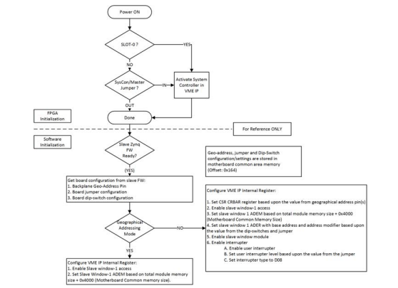
Note
VME 64XXX CCA Address Configuration Power-On Initialization Flow Chart - For reference ONLY
Switch and Jumper Definitions
Note
Illustration not to scale
| Reference Only / GPIO# | Switch | Description |
|---|---|---|
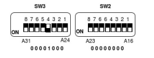
| 42 ~ 49 | SW3-8:1 MSB | VME Base Address [31:24] ON = 0 OFF = 1 |
| 34 ~ 41 | SW2-8:1 LSB | VME Base Address [23:16] |
| Reference Only / GPIO# | Switch | Description |
|---|---|---|
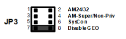
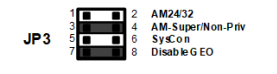
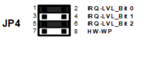
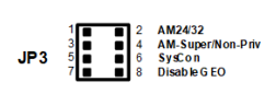
| 17 | JP3-1:2 A24/A32 Address Modifier | IN = A24 OUT = A32 (Default) |
| 18 | JP3-3:4 Supervisory/non-privileged Address Modifier | IN = Supervisory OUT = Non-privileged (Default) |
| 19 | JP3-5:6 System Controller | IN = Enable System Controller OUT = Disable System Controller (Default) |
| 20 | JP3-7:8 Geographical Address | IN = Disable Geographic Addressing OUT = Enable Geographic Addressing (Default) |
| 23 | JP4-1:2 IRQ_LV_BIT0 | IN = 0 OUT = 1 (Default) 001 |
| 24 | JP4-3:4 IRQ_LV_BIT1 | IN = 0 OUT = 1 (Default) 010 |
| 25 | JP4-5:6 IRQ_LV_BIT2 | IN = 0 OUT = 1 (Default) 100 |
| HW_WP (REF 64ARM1 only) | JP4-7:8 SATA Disk Write Protect | IN = Disable Write Protect OUT = Enable Write Protect |
Note
Dip-switch, jumper, and geographic address configuration saved in motherboard common memory at offset 0x164 - For reference ONLY
| Bit | Description | [31:24] | SW3: MSB of VME Address A31- A24 | [23:16] | SW2: LSB of VME Address A23 - A16 | [15:8] | Bit 8-12: Geographic Address value from VME64 chassis slot address |
| Bit 13: Geographic Address Parity | Bit14-15: Reserved | [0:7] | JP3 and JP4: | Bit 0: 1= AM-A32, 0=AM-A24 | Bit 1: 1= AM-Non-privileged, 0=AM-Supervisory | Bit 2: 1= Slave, 0=System Controller | |
| Bit 3: 1= Geo, 0=Non-Geo | Bit 4-6: IRQ_LV [0:3] 3bits | Bit 7: Reserved | |||||
Slave Support/Configuration
The VME slave interface will support following data transfer mode and interrupter type:
Addressing Mode
A32, A24
Data Type
D32, D16, D08
Note
D32 is recommended to be the default standard data type. The GEN5 boards module data is provided as 32-bit R/W register access. If another data type is used, accommodations must be made in the software application for data translation.
Access Mode
Read, Write
Interrupter
Level 1 ~ 7 and Type D08
Address Modifier
| A32 Address Modifier | A24 Address Modifier | |
| Geographical | 0x0E: supervisory program access | 0x3E: supervisory program access |
| 0x0D: supervisory data access | 0x3D: supervisory data access | |
| 0x0A: non-privileged program access | 0x3A: non-privileged program access | |
| 0x09: non-privileged data access | 0x39: non-privileged data accessing | |
| 0x2F: CR/CSR Space | ||
| Non-geographical | 0x0D: supervisory data access | 0x3D: supervisory data access |
| 0x09: non-privileged data access | 0x39: non-privileged data accessing |
Non-Geographical Addressing Configuration
The following describes setting the base address of the board via the hardware DIP switches.
Disable geographical addressing mode by placing a jumper-shunt across JP3-7:8
Configure/set the VME base address of the card:
- Use switch SW3 and SW2 to configure the base address of the card.
- Default address from the factory is 0x0000 0000
- Use SW3 for A31-A24 and SW2 for A23-A16 (by default, A15 - A0 are reserved and set to 0x0000)
Example:
Base address: 0x0800 0000
Configure the address modifiers: Use JP3-1:2 (for A24 (in) /A32 (out) selection) and JP3-3:4 (for Supervisory (in) / No-Privileged data access selection (out))
Example:
Address Modifier set for: to 0x0D, A32 supervisory data access (Geographical mode disabled).
Configure Interrupter Level
-
Use JP4-1:2, JP4-3:4, JP4-5:6 to configure the interrupter level from level 7 ~ 1.
-
Each jumper represents a bit of a 3-bit configuration where default (open) level is 7 or “1 - 1 - 1”.
Example:
Set the interrupter level to 2 by insert a jumper into JP4-5:6 and JP4-1:2 to mask out bit0 and bit2
Geographical Addressing Configuration
Enable geographical addressing mode by removing/ensuring jumper JP3-7:8 is not installed.
When geographical addressing configuration mode is enabled (by removing jumper-shunt on JP3-7:8), JP3-3:4 and JP4-(all) jumper configurations are effectively ignored.
The card will ONLY respond to 0x2F A24-CR/CSR address modifier when geographical addressing mode is enabled.
Configuring base address, address modifier, enable slave window and enable the interrupter of a card can be accomplished by using CR/CSR configuration space on a card. The address of CR/CSR is based on the geographic slot# from a VME64 backplane.
| Slot# | VME64 Back Plane Address | CSR Address |
|---|---|---|
| 1 | 0x3E | 0x080000 |
| 2 | 0x3D | 0x100000 |
| 3 | 0x1C | 0x180000 |
| 4 | 0x3B | 0x200000 |
| 5 | 0x1A | 0x280000 |
| 6 | 0X19 | 0x300000 |
| 7 | 0x38 | 0x380000 |
| 8 ~ 21 | 0x37 ~ 0x2A | 0x400000 ~ 0xA80000 |
Example:
Configure the Geographical Address of a card in slot# 2 of the VME64x chassis.
The CSR base address of a card in slot# 2 is 0x100000 and size of CSR space is 512 KB (offset range: 0x7FFFF ~ 0x0).
-
Setup/program a base address: 0x8000000. a. Write 0x08 to 0x17FF60 (CSR_ADER0 A32-A24) b. Write 0x00 to 0x17FF64 (CSR_ADER0 A23-A16)
-
Setup address modifier: 0x39 / A24 non-privileged data access. a. Write 0xE4 (0x39 << 2) to 0x17FF6C (CSR_ADER0 AM[5:0] )
-
Enable card slave window module. a. Write 0x10 to 0x17FFF8 (CSR_BIT_SET Enable Module)
-
Enable interrupter: level 7. a. Write 0x70 to 0x17F83B (Interrupter level map to 7) b. Write 0x02 to 0x17F80B (Enable Interrupter)
The card will now respond to the base address (0x800 0000 in the example) with address modifier (0x39 / A24 non-privileged data access: 0x0800 0000.
System Controller Support
There are 2 ways to enable the system controller function on the card:
-
Automatic: When a card is installed and recognized in SLOT-0 of a VME64x chassis.
-
Manual: Adding a jumper to JP3-5:6 will force the card to enable system controller function
Note
There can only be one system controller card in a VMEbus chassis.
Slave Window Base Address Boundary
The slave window base address boundary of each card range is from 256 Byte to 8 Megabyte. The base address boundaries are based on total size of all functional modules available on the card.
Example:
| Base address: | 0x0800 0000 |
| Card common memory size = | 16 Kilobyte |
| Slot 1 module size = | 16 Kilobyte |
| Slot 2 module size = | 16 Kilobyte |
| Slot 3 module size = | 1 Megabyte |
| Slot 4 module size = | Empty |
| Slot 5 module size = | Empty |
| Slot 6 module size = | Empty |
| Total memory size: | 16 KB ` 16 KB ` 16 KB + 1 MB = 1.05 MB (Rounds of the total size to 2 MB 0x200000) |
| Card base address boundaries = | 0x08000000 ~ 0x081FFFFF |
ETHERNET
(For detailed supplement, please visit the NAI web-site specific product page and refer to: Ethernet Interface for Generation 5 SBC and Embedded IO Boards Specification)
Note
For products capable of 10/100/1000Base-KX functionality - the product Ethernet PHY supports 1000BASE-X. Product interoperability with 10/100/1000BASE-KX is supported with 1000BASE-X (provided that auto-negotiation is disabled).
The Ethernet Interface Option allows communications and control access to all function modules either via the system BUS or Ethernet ports 1 or 2.
Ethernet 1 Ethernet 2 Ethernet 3* Ethernet 4* (REF PORT A) (REF PORT B) (REF PORT C) (REF PORT D) The default IP address: 192.168.1.16 192.168.2.16 192.168.3.16 192.168.4.16 The default subnet: 255.255.255.0 255.255.255.0 255.255.255.0 255.255.255.0 The default gateway: 192.168.1.1 192.168.2.1 192.168.3.1 192.168.4.1 *see Part Number Designation for applicability.
Note
Actual “as shipped” card Ethernet default IP addresses may vary based upon final ATP configuration(s).
The NAI interface supports IPv4 and IPv6 and both the TCP and UDP protocols. The Ethernet Operation Mode Command Listener application running on the motherboard host processor implements the operation interface. The listener is operational on startup through the nai_MBStartup process and listen on specific ports for commands to process. The default ports are listed below:
- TCP1 - Port 52801
- TCP2 - Port 52802
- UDP1 - Port 52801
- UDP2 - Port 52802
While the listener is active, note that interrupts from the motherboard do not trigger. The listener can be disabled by turning off the nai_MBStartup process through the Motherboard EEPROM. To turn off nai_MBStartup use the command mbeeprom_util set MBStartupInitOnlyFlag 1 in the console, either by serial port or telnet to the motherboard, and then reboot the system. To turn on the nai_MBStartup use the command mbeeprom_util set MBStartupInitOnlyFlag 0 in the console, either by serial port or telnet to the motherboard, and then reboot the system.
Ethernet Message Framework
The interface uses a specific message framework for all commands and responses. All messages begin with a Preamble code and end with a Postamble code. The message framework is shown below.
Preamble
2 bytes Always
0xD30FSequenceNo
2 bytesType Code
2 byteMessage Length
(2 bytes)Payload
(0..1414 bytes)Postamble
2 bytes
Always
0xF03DMessage Elements
Preamble The Preamble is used to delineate the beginning of a message frame.
The Preamble is always 0xD30F.SequenceNo The SequenceNo is used to associate Commands with Responses. Type Code Type Codes are used to define the type of Command or Response the message contains. Message Length The Message Length is the number of bytes in the complete message frame starting with and including the
Preamble and ending with and including the Postamble.Payload The Payload contains the unique data that makes up the command or response.
Payloads vary based on command type.Postamble The Postamble is use to delineate the end of a message frame.
The Postamble is always 0xF03D.Notes
- The messaging protocol applies only to card products.
- Messaging is managed by the connected (client) computer. The client computer will send a single message and wait for a reply from the card. Multiple cards may be managed from a single computer, subject to channel and computer capacity.
Board Addressing
The interface provides two main addressing areas: Onboard and Off-board.
Onboard addressing refers to accessing resources located on the board that is implementing the operation interface (including its modules).
Off-board addressing refers to accessing resources located on another board reachable via VME, PCI, or other bus. Off-board addressing requires a Master/Slave configuration.
The user must always specify if a particular address is Onboard or Off-board. See the command descriptions for the onboard and off-board flags.
Within a particular board (Onboard or Off-board), the address space is broken up into two areas: Motherboard Common Address Space and Module Address Space. All addresses are 32-bit.
Motherboard Common Address Space starts at 0x00000000 and ends at 0x00004000. This is a 4Kx32-bit address space (16 kbytes).
Module Address Space starts at 0x00004000. Module addressing is dynamically configured at startup. NAI boards support between 1 and 6 modules. The minimum module address space size is 4Kx32 (16 kbytes) and module sizes are always a multiple of 4Kx32.
Module addressing is dynamic and cumulative. The first detected module (starting with Slot 1) is given an address of 0x00004000. The 2nd detected Module is given an address of:
First_Detected_Module_Address + First_Detected_Module_Size
Note
Slots do not define addresses.
If no module is detected in a module slot, that slot is not given an address. Therefore, if the first detected Module is in Slot 2, then that module address will be 0x00004000. If the next detected module is in Slot 4, then the address of that Module will be:
Second_Detected_Module_Address = First_Detected_Module_Address + First_Detected_Module_Size
If a 3rd Module is detected in Slot 6, then the address of that Module will be:
Third_Detected_Module_Address = Second_Detected_Module_Address + Second_Detected_Module_Size
Note
Module addresses are calculated at each board startup when the modules are detected. Therefore, if a module should fail to be detected due to malfunction or because it was removed from the motherboard, the addresses of the modules that follow it in the slot sequence will be altered. This is important to note when programming to this interface.
Users can always retrieve the Module Addresses, Module Sizes and Module IDs from the fixed Motherboard Common address area. This data is set upon each board startup. While the Module Addressing is dynamic, the address where these addresses are stored is fixed. For example, to find the startup address of the module location in Slot 3, refer to the MB Common Address 0x00000408 from the Motherboard Common Addresses table that follows.
Ethernet Wiring Convention
Link to original
RJ-45 Pin T568A Color T568B Color 10/100Base-T 1000BASE-T NAI wiring convention 1 white/green stripe white/orange stripe TX+ DA+ ETH-TP0+ 2 green orange TX- DA- ETH-TP0- 3 white/orange stripe white/green stripe RX+ DB+ ETH-TP1+ 4 blue blue DC+ ETH-TP2+ 5 white/blue stripe white/blue stripe DC- ETH-TP2- 6 orange green RX- DB- ETH-TP1- 7 white/brown stripe white/brown stripe DD+ ETH-TP3+ 8 brown brown DD- ETH-TP3-
CONNECTOR/PIN-OUT INFORMATION
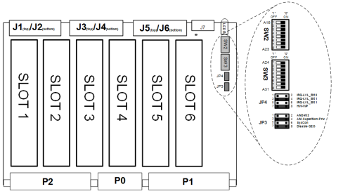
The 6U VME SBC &/or Multifunction I/O board is available in two configurations: convection or conduction cooled. I/O connections are provided via the (J1-J6) front panel connectors and/or through the user defined rear I/O connectors P2 and P0 (VME64x) (see part number and pin-out information) when defined.

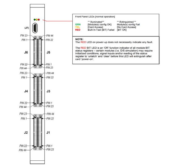
Front Panel Connectors J1 - J6 (Convection-Cooled)
44-pin male connectors, 2mm, Harwin P/N M80-5114422.
Mate kit: “Custom Hood Kit” part # M80C108448C (or equivalent); Includes connector, backshell, pins & jackscrews. This mating connector kit may be purchased separately as NAI P/N 05-0119 (contact factory).
Panel LEDs
Front Panel LEDs indications (only available on air-cooled units).
| LED | ILLUMINATED | EXTINGUISHED |
|---|---|---|
| GRN: | Blinking: Initializing Steady On: Power-On/Ready | Power off |
| RED: | Module BIT fault | No BIT fault |
| YEL: | (flash) Card access (bus or Gig-E activity) | No card activity |
Chassis Ground
| Front Panel Connectors: | J1 - J6 pin-1 is chassis GND. Jack screw sockets are chassis GND. |
|---|---|
| Rear Connectors: | Not available. |
Front Panel System (Power/Signal) Ground Reference
| Front Panel: | J1 - J6 pin-23 is System (SYS) GND (referenced to card power/system ground). |
|---|
Front IO Utility Connector J7 (Convection and Conduction-Cooled)
The card utilizes a Mini-HDMI (Type-C) type card edge receptacle J7, available on either convection or conduction-cooled configurations that provides the following signal interfaces:
- Serial (RS-232 debug/console only)
- Ethernet port 1 (factory configuration option - Ethernet port 1 may be redirected to rear I/O J2)
NAI also provides an optional front panel utility connector breakout adapter kit which includes a “breakout” adapter board and a 1-meter miniHDMI to mini-HDMI type cable. The breakout adapter kit provides standard connector I/O connections to Ethernet (RJ-45 receptacle) and asynchronous serial (DB9P) (if applicable). The optional breakout adapter kit may be purchased separately as NAI P/N 75SBC4-BB. Consult the factory for availability
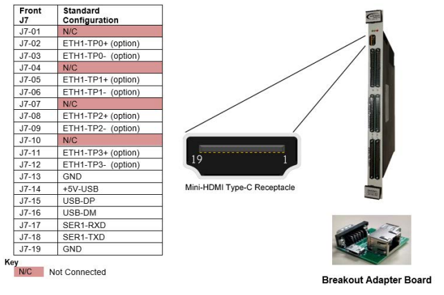
Signal Descriptions J7
| Signal Name | Description |
|---|---|
| ETH1-TPx | Ethernet port 1 signals (4 pair) 10/100/1000 twisted pair signals (Optional - available only if NOT re-directed to rear I/O (see part number configuration options) |
| USB-DP | Front Panel USB Data Plus |
| USB-DM | Front Panel USB Data Minus |
| SER1-TXD | Asynchronous transmit serial data port 1 (out) / RS232 debug/console port only |
| SER1-RXD | Asynchronous received serial data port 1 (in) / RS232 debug/console port only |
| GND | System Ground (return) |
Rear I/O VME Card Connectors P0-P2 Signal Summary
The SBC &/or multifunction I/O board provides interface via the rear VME card connectors.
Rear I/O Summary
| P0 - User I/O and Ethernet Interface connector. |
|---|
| P1 - VME/Utility (Primary) connector. Contains the following signal definitions: | |
| Power: | Primary `5V, `/- 12V and System GND |
| Geographical Address Pins: | GA0# - GA4#, GAP# |
| Card reset: | SYSRST# signal |
| VME Interface | Primary control, data bus D0-D15, address bus A1-A23 |
| P2 - User I/O (Secondary) and VME/Utility (Extended) connector. | |
| Power: | Additional +5V and System GND |
| VME Interface | Extended control, data bus D16-D31, address bus A24-A31 |
| User I/O | See table below |
User Rear I/O / Module Signal Distribution
| Module # | P0 | P2 | 1 |
| N/A | DataIO 01-32 | 2 | DataIO 25-32 |
| DataIO 01-24 | 3 | DataIO 01-32 | N/A |
| 4 | DataIO 01-16 | DataIO 17-24 | DataIO 25-32 |
| 5 | DataIO 01-24 | ||
| DataIO 25-32 | 6 | DataIO 19-24 | DataIO 01-18 |
| DataIO 25-32 or ETH2 option |
Rear User I/O and Ethernet Interface Connector (P0)
The P0 connector provides User I/O, Ethernet Interface options and Utility (Extended) signal(s) for the board. Signals defined as N/C currently have no functionality associated and is not required for general operation.
VME/Utility (Primary) Interface Connector P1 (Reference)
The P1 connector provides VME/Utility (Primary) signals for the board. Signals defined as N/C currently have no functionality associated and is not required for general operation.
| VME | Row | Row | Row | Row | Row |
|---|---|---|---|---|---|
| P1 | A | B | C | D | E (Z) |
| 1 | VME-D0 | VME-BBSY# | VME-D8 | N/C | N/C |
| 2 | VME-D1 | VME-BCLR# | VME-D9 | GND | GND |
| 3 | VME-D2 | VME-ACFAIL# | VME-D10 | N/C | N/C |
| 4 | VME-D3 | VME-BGIN0# | VME-D11 | N/C | GND |
| 5 | VME-D4 | VME-BGOUT0# | VME-D12 | N/C | N/C |
| 6 | VME-D5 | VME-BGIN1# | VME-D13 | N/C | GND |
| 7 | VME-D6 | VME-BGOUT1# | VME-D14 | N/C | N/C |
| 8 | VME-D7 | VME-BGIN2# | VME-D15 | N/C | GND |
| 9 | GND | VME-BGOUT2# | GND | VME-GAP# | N/C |
| 10 | VME-SYSCLK | VME-BGIN3# | VME-SYSFAIL# | VME-GA0# | GND |
| 11 | GND | VME-BGOUT3# | VME=BERR# | VME-GA1# | N/C |
| 12 | VME-DS1# | VME-BR0# | VME-SYSRST# | N/C | GND |
| 13 | VME-DS0# | VME-BR1# | VME-LWORD# | VME-GA2# | N/C |
| 14 | VME-WRITE# | VME-BR2# | VME-AM5 | N/C | GND |
| 15 | GND | VME-BR3# | VME-A23 | VME-GA3# | N/C |
| 16 | VME-DTACK# | VME-AM0 | VME-A22 | N/C | GND |
| 17 | GND | VME-AM1 | VME-A21 | VME-GA4# | N/C |
| 18 | VME-AS# | VME-AM2 | VME-A20 | N/C | GND |
| 19 | GND | VME-AM3 | VME-A19 | N/C | N/C |
| 20 | VME-IACK# | GND | VME-A18 | N/C | GND |
| 21 | VME-IACKIN# | N/C | VME-A17 | N/C | N/C |
| 22 | VME-IACKOUT# | N/C | VME-A16 | N/C | GND |
| 23 | VME-AM4 | GND | VME-A15 | N/C | N/C |
| 24 | VME-A7 | VME-IRQ7# | VME-A14 | N/C | GND |
| 25 | VME-A6 | VME-IRQ6# | VME-A13 | N/C | N/C |
| 26 | VME-A5 | VME-IRQ5# | VME-A12 | N/C | GND |
| 27 | VME-A4 | VME-IRQ4# | VME-A11 | N/C | N/C |
| 28 | VME-A3 | VME-IRQ3# | VME-A10 | N/C | GND |
| 29 | VME-A2 | VME-IRQ2# | VME-A9 | N/C | N/C |
| 30 | VME-A1 | VME-IRQ1# | VME-A8 | N/C | GND |
| 31 | (-)12 | N/C | (+)12 | GND | N/C |
| 32 | (`)5V | (`)5V | (+)5V | N/C | GND |
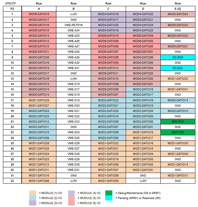
Rear User I/O & Extended VME Interface Connector (P2)
The P2 connector provides User I/O and VME/Utility (Extended) signals for the board. Signals defined as N/C currently have no functionality associated and is not required for general operation.
Front Panel Connector and LED Indicator Layout (Convection-Cooled)
The following provides the connector layout and pinout data for the Front Panel connectors J1-J6.
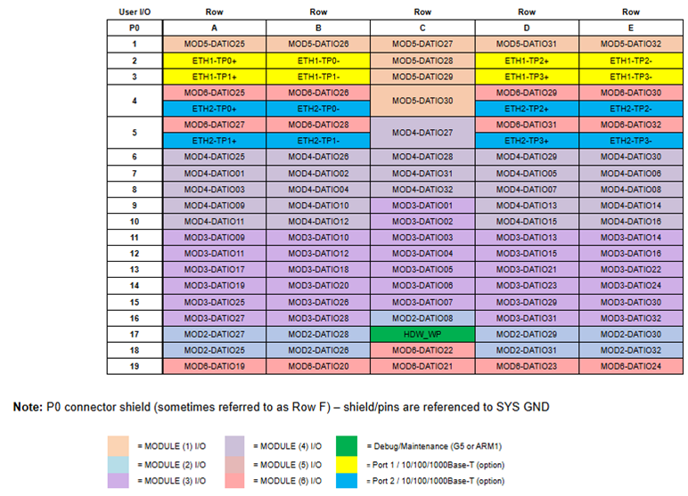
Front and Rear User I/O Mapping
Pin-out details (for reference) are shown below, with respect to DATAIO. Additional information on pin-outs can be found in the Module Operational Manuals
| Slot 1 | Slot 2 | Slot 3 | ||||||||
| Module Signal (Ref Only) | Front I/O J1 44-pin | Rear I/O P2 | Global (MB) | Front I/O J2 44-pin | Rear I/O P0 | Rear I/O P2 | Global (MB) | Front I/O J3 44-pin | Rear I/O P0 | Global (MB) |
| DATIO1 | 2 | 30D | 2 | 22D | 2 | 9C | ||||
| DATIO2 | 24 | 29D | 24 | 21D | 24 | 10C | ||||
| DATIO3 | 3 | 28D | 3 | 20D | 3 | 11C | ||||
| DATIO4 | 25 | 27D | 25 | 19D | 25 | 12C | ||||
| DATIO5 | 5 | 32C | 5 | 24C | 5 | 13C | ||||
| DATIO6 | 27 | 31C | 27 | 23C | 27 | 14C | ||||
| DATIO7 | 7 | 30C | 7 | 22C | 7 | 15C | ||||
| DATIO8 | 29 | 29C | 29 | 21C | 29 | 16C | ||||
| DATIO9 | 8 | 32A | 8 | 24A | 8 | 11A | ||||
| DATIO10 | 30 | 31A | 30 | 23A | 30 | 11B | ||||
| DATIO11 | 10 | 30A | 10 | 22A | 10 | 12A | ||||
| DATIO12 | 32 | 29A | 32 | 21A | 32 | 12B | ||||
| DATIO13 | 12 | 31Z | 12 | 19Z | 12 | 11D | ||||
| DATIO14 | 34 | 29Z | 34 | 17Z | 34 | 11E | ||||
| DATIO15 | 13 | 26D | 13 | 18D | 13 | 12D | ||||
| DATIO16 | 35 | 25D | 35 | 17D | 35 | 12E | ||||
| DATIO17 | 15 | 24D | 15 | 16D | 15 | 13A | ||||
| DATIO18 | 37 | 23D | 37 | 15D | 37 | 13B | ||||
| DATIO19 | 17 | 28C | 17 | 20C | 17 | 14A | ||||
| DATIO20 | 39 | 27C | 39 | 19C | 39 | 14B | ||||
| DATIO21 | 18 | 26C | 18 | 18C | 18 | 13D | ||||
| DATIO22 | 40 | 25C | 40 | 17C | 40 | 13E | ||||
| DATIO23 | 20 | 28A | 20 | 20A | 20 | 14D | ||||
| DATIO24 | 42 | 27A | 42 | 19A | 42 | 14E | ||||
| DATIO25 | 4 | 26A | 4 | 18A | 4 | 15A | ||||
| DATIO26 | 26 | 25A | 26 | 18B | 26 | 15B | ||||
| DATIO27 | 9 | 18A | 9 | 17A | 9 | 16A | ||||
| DATIO28 | 31 | 17A | 31 | 17B | 31 | 16B | ||||
| DATIO29 | 14 | 27Z | 14 | 17D | 14 | 15D | ||||
| DATIO30 | 36 | 25Z | 36 | 17E | 36 | 15E | ||||
| DATIO31 | 19 | 15Z | 19 | 18D | 19 | 16D | ||||
| DATIO32 | 41 | 13Z | 41 | 18E | 41 | 16E | ||||
| DATIO33 | 6 | 6 | 6 | |||||||
| DATIO34 | 28 | 28 | 28 | |||||||
| DATIO35 | 11 | 11 | 11 | |||||||
| DATIO36 | 33 | 33 | 33 | |||||||
| DATIO37 | 16 | 16 | 16 | |||||||
| DATIO38 | 38 | 38 | 38 | |||||||
| DATIO39 | 21 | 21 | 21 | |||||||
| DATIO40 | 43 | 43 | 43 | |||||||
| N/A | 23 | SYS GND | 23 | * | * | SYS GND | 23 | * | SYS GND | |
| 1 | CHASSIS | 1 | CHASSIS | 1 | CHASSIS | |||||
| 22, 44 | N/C | 22, 44 | N/C | 22, 44 | N/C | |||||
Notes
| * | Rear I/O system GND (J2): A19, B1, B3, B19-B21, D16, E9 (SER-GND), F1-F22 (analog I/O modules except Slot 1) See rear I/O (SYS) GND (all other modules) |
|---|
| Slot 4 | Slot 5 | Slot 6 | ||||||||||
| Module Signal (Ref Only) | Front I/O J4 44-pin | Rear I/O P0 | Rear I/O P2 | Global (MB) | Front I/O J5 44-pin | Rear I/O P0 | Rear I/O P2 | Global (MB) | Front I/O J5 44-pin | Rear I/O P0 | Rear I/O P2 | Global (MB) |
| DATIO1 | 2 | 7A | 2 | 14D | 2 | 8D | ||||||
| DATIO2 | 24 | 7B | 24 | 13D | 24 | 7D | ||||||
| DATIO3 | 3 | 8A | 3 | 12D | 3 | 6D | ||||||
| DATIO4 | 25 | 8B | 25 | 11D | 25 | 5D | ||||||
| DATIO5 | 5 | 7D | 5 | 10D | 5 | 10C | ||||||
| DATIO6 | 27 | 7E | 27 | 9D | 27 | 9C | ||||||
| DATIO7 | 7 | 8D | 7 | 16C | 7 | 8C | ||||||
| DATIO8 | 29 | 8E | 29 | 15C | 29 | 7C | ||||||
| DATIO9 | 8 | 9A | 8 | 14C | 8 | 6C | ||||||
| DATIO10 | 30 | 9B | 30 | 13C | 30 | 5C | ||||||
| DATIO11 | 10 | 10A | 10 | 12C | 10 | 8A | ||||||
| DATIO12 | 32 | 10B | 32 | 11C | 32 | 7A | ||||||
| DATIO13 | 12 | 9D | 12 | 16A | 12 | 6A | ||||||
| DATIO14 | 34 | 9E | 34 | 15A | 34 | 5A | ||||||
| DATIO15 | 13 | 10D | 13 | 14A | 13 | 4A | ||||||
| DATIO16 | 35 | 10E | 35 | 13A | 35 | 3A | ||||||
| DATIO17 | 15 | 2C | 15 | 12A | 15 | 2A | ||||||
| DATIO18 | 37 | 1C | 37 | 11A | 37 | 1A | ||||||
| DATIO19 | 17 | 4C | 17 | 10A | 17 | 19A | ||||||
| DATIO20 | 39 | 3C | 39 | 9A | 39 | 19B | ||||||
| DATIO21 | 18 | 2D | 18 | 7Z | 18 | 19C | ||||||
| DATIO22 | 40 | 1D | 40 | 5Z | 40 | 18C | ||||||
| DATIO23 | 20 | 4D | 20 | 3Z | 20 | 19D | ||||||
| DATIO24 | 42 | 3D | 42 | 1Z | 42 | 19E | ||||||
| DATIO25 | 4 | 6A | 4 | 1A | 4 | 4A | ||||||
| DATIO26 | 26 | 6B | 26 | 1B | 26 | 4B | ||||||
| DATIO27 | 9 | 5C | 9 | 1C | 9 | 5A | ||||||
| DATIO28 | 31 | 6C | 31 | 2C | 31 | 5B | ||||||
| DATIO29 | 14 | 6D | 14 | 3C | 14 | 4D | ||||||
| DATIO30 | 36 | 6E | 36 | 4C | 36 | 4E | ||||||
| DATIO31 | 19 | 7C | 19 | 1D | 19 | 5D | ||||||
| DATIO32 | 41 | 8C | 41 | 1E | 41 | 5E | ||||||
| DATIO33 | 6 | 6 | 6 | |||||||||
| DATIO34 | 28 | 28 | 28 | |||||||||
| DATIO35 | 11 | 11 | 11 | |||||||||
| DATIO36 | 33 | 33 | 33 | |||||||||
| DATIO37 | 16 | 16 | 16 | |||||||||
| DATIO38 | 38 | 38 | 38 | |||||||||
| DATIO39 | 21 | 21 | 21 | |||||||||
| DATIO40 | 43 | 43 | 43 | |||||||||
| N/A | 23 | * | * | SYS GND | 23 | * | * | SYS GND | 23 | * | * | SYS GND |
| 1 | CHASSIS | 1 | CHASSIS | 1 | CHASSIS | |||||||
| 22, 44 | N/C | 22, 44 | N/C | 22, 44 | N/C | |||||||
Notes:
| * | Rear I/O system GND (J2): A19, B1, B3, B19-B21, D16, E9 (SER-GND), F1-F22 (analog I/O modules except Slot 1) See rear I/O (SYS) GND (all other modules) |
|---|---|
| 4/5(x) | Rear I/O is available only if rear Ethernet port 2 is NOT specified |
Ethernet (Rear I/O)
Optional - See Part Number Designation section for specific configuration.
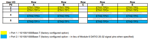
Commercial Equivalent RJ45-type Ethernet cabling/wiring (for reference only):
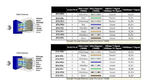
Connector Signal/Pin-Out Notes
NAI Synchro/Resolver Naming Convention
| Signal | Resolver | Synchro |
|---|---|---|
| S1 | SIN(-) | X |
| S2 | COS(+) | Z |
| S3 | SIN(+) | Y |
| S4 | COS(-) | No connect |
Additional Pin-Out Notes
| 1. Isolated Discrete Module (DT2) | For ‘differential’ A/D; “P” designation considered ‘positive’ input pin, “N” pin designation considered ‘negative’ input pin. |
|---|---|
| 2. Discrete I/O Module (DT1) | All GND pins are common within the module, but, isolated from |
| system/power GND. Each pin should be individually wired for optimal | power current distribution. |
| 3. TTL I/O Module (TL1) | I/O referenced to system power GND. |
| 4. CMRP - A/D Module(s) (ADx) | The Common Mode Reference Point (CMRP) is an isolated reference connection for all the A/D channels. For expected high common mode voltage applications, it is recommended that the pin designated as CMRP be referenced (direct or resistor coupled) to the signal source GND reference (must have current path between CMRP and signal source generator) to minimize common mode voltage within the acceptable specification range. All channels within the module are independent but share a CMRP, which is isolated from system/power GND. |
MECHANICAL DETAILS
General - Outline
The following mechanical outline detail examples are provided for reference only. Dimensions are in inches, unless otherwise specified.
Conduction Cooled
Convection Cooled
64ARM1 PART NUMBER DESIGNATION
Click here for the 64AR1 part number designation
SYNCHRO/RESOLVER AND LVDT/RVDT SIMULATION MODULE CODE TABLES
Select the Digital-to-Synchro (DSx), Digital-to-Resolver (DRx) or Digital-to-LVDT/RVDT (DLx) module ID corresponding to the application operating parameters required from the following code table (where x = the specific module ID designator). Customer should indicate the actual frequency applicable the design to assure that the correct default band width is set at the factory. All Input and Reference voltages are auto ranging. Frequency/voltage band tolerances +/- 10%. For availability and ranges other than those listed contact the factory. Specifications may be subject to change.
- Single Channel module pending availability (contact factory)
Module ID Format Channel(s) Output Voltage VL-L (Vrms) Reference Voltage (Vrms) Frequency Range (Hz) Power / CH maximum (VA) Notes DS1 SYN 1* 2 - 28 2 - 115 47 - 1 K 3 DR1 RSL DL1 LVDT/RVDT DS2 SYN 1* 2 - 28 2 - 115 1 K - 5 K 3 DR2 RSL DL2 LVDT/RVDT DS3 SYN 1* 2 - 28 2 - 115 5 K - 10 K 3 DR3 RSL DL3 LVDT/RVDT DS4 SYN 1* 2 - 28 2 - 115 10 K - 20 K 3 DR4 RSL DL4 LVDT/RVDT DS5 SYN 1* 28 - 90 2 - 115 47 - 1 K 3 DR5 RSL DL5 LVDT/RVDT DSX SYN 1* X X X X X = TBD; special configuration, requires special part number code designation, contact factory DRX RSL DLX LVDT/RVDT DSA SYN 2 2 - 28 2 - 115 47 - 1 K 1.5 DRA RSL DLA LVDT/RVDT DSB SYN 2 2 - 28 2 - 115 1 K - 5 K 1.5 DRB RSL DLB LVDT/RVDT DSC SYN 2 2 - 28 2 - 115 5 K - 10 K 1.5 DRC RSL DLC LVDT/RVDT DSD SYN 2 2 - 28 2 - 115 10 K - 20 K 1.5 DRD RSL DLD LVDT/RVDT DSE SYN 2 28 - 90 2 - 115 47 - 1 K 2.2 DRE RSL DLE LVDT/RVDT DSY SYN 2 Y Y Y Y Y = TBD; special configuration, requires special part number code designation, contact factory DRY RSL DLY LVDT/RVDT DSJ SYN 3 2 - 28 2 - 115 47 - 1 K 0.5 DRJ RSL DLJ LVDT/RVDT DSK SYN 3 2 - 28 2 - 115 1 K - 5 K 0.5 DRK RSL DLK LVDT/RVDT DSL SYN 3 2 - 28 2 - 115 5 K - 10 K 0.5 DRL RSL DLL LVDT/RVDT DSM SYN 3 2 - 28 2 - 115 10 K - 20 K 0.5 DRM RSL DLM LVDT/RVDT DSN SYN 3 28 - 90 2 - 115 47 - 1 K 0.5 DRN RSL DLN LVDT/RVDT DSZ SYN 3 Z Z Z Z Z = TBD; special configuration, requires special part number code designation, contact factory DRZ RSL DLZ LVDT/RVDT SYNCHRO/RESOLVER AND LVDT/RVDT MEASUREMENT MODULE CODE TABLES
SYN/RSL Four-Channel Measurement (Field Programmable SYN/RSL)
Select the Synchro/Resolver-to-Digital (SDx) module ID corresponding to the application operating parameters required from the following code table (where x = the specific module ID designator). Customer should indicate the actual frequency applicable to the design to assure that the correct default band width is set at the factory. All Input and Reference voltages are auto ranging. For availability and ranges other than those listed contact the factory. Specifications may be subject to change.
Frequency/voltage band tolerances +/- 10%.
Module ID Input Voltage V (Vrms) Reference Voltage + (Vrms) Frequency Range + (Hz) Notes SD1 2 - 28 2 - 115 47 - 1 K SD2 2 - 28 2 - 115 1K - 5 K SD3 2 - 28 2 - 115 5K - 10 K SD4* 2 - 28 2 - 115 10K - 20 K SD5 28 - 90 2 - 115 47 - 1 K SDX* X X X X = TBD; special configuration, requires special part number code designation, contact factory *Consult factory for availability
LVDT/RVDT Four-Channel Measurement (Field Programmable 2, 3 or 4-Wire)
Select the LVDT/RVDT-to-Digital (LDx) module ID corresponding to the application operating parameters required from the following code table (where x = the specific module ID designator). Customer should indicate the actual frequency applicable to the design to assure that the correct default band width is set at the factory. All Input and Excitation voltages are auto ranging. For availability and ranges other than those listed contact the factory. Specifications may be subject to change.
Frequency/voltage band tolerances +/- 10%.
Module ID Input Signal Voltage V + (Vrms) Excitation Voltage + (Vrms) Frequency Range + (Hz) Notes LD1 2 - 28 2 - 115 47 - 1 K LD2 2 - 28 2 - 115 1K - 5 K LD3 2 - 28 2 - 115 5K - 10 K LD4* 2 - 28 2 - 115 10K - 20 K LD5 28 - 90 2 - 115 47 - 1 K LDX* X X X X = TBD; special configuration, requires special part number code designation, contact factory *Consult factory for availability
Link to original
APPENDIX: EMBEDDED ARM (XILINX® XC7Z015 SOC) OPTION DETAILS
If specified, the PLATFORM (e.g. NIU1A, 75G5, etc.) provides access to an ARM processor for embedded SBC-type applications. The platform uses a Xilinx® XC7Z015 SoC FPGA device. This device is a Single-die system on a Chip (SoC) that consists of two distinct parts: an application processor unit (APU) portion and an FPGA portion. The platform may be ordered with a configuration code, which provides access to the motherboards APU ARM processor. The application processor system can then be used for customer software development. The PLATFORM uses a Xilinx® XC7Z015 device with an ARM® Cortex®-A9 dual-core processor. The ARM processor, together with NAI’s unique architecture provides the embedded system programmer the following on- chip resources:
- APU subsystem featuring dual ARM Cortex-A9 MPCore CPUs
- DDR3 SDRAM controller with Transaction Scheduler
- DMA controller with scatter-gather
- Two Ethernet Media Access Controllers (EMACs)
- NAND flash controller ONFI specification 1.0
- Quad SPI flash controller
- Two serial peripheral interface (SPI) Master or Slave controllers
- 256 KB on-chip RAM
- 128 KB on-chip boot ROM
- Two UARTs with 64-byte receive and transmit FIFOs
- Two General Purpose Timers
- Two watchdog timers
Floating Point Unit (FPU)
The FPU is a VFPv3-D16 implementation of the ARMv7 floating-point architecture. It provides high performance, floating-point computation. The FPU supports all addressing modes and operations described in the “ARM Architecture Reference Manual”. The manual is available from several sources on the internet. The FPU features are:
- Support for single-precision and double-precision floating-point formats
- Support for conversion between half-precision and single-precision
- High data transfer bandwidth through 64-bit split load and store buses
- Completion of load transfers can be performed out-of-order
- Normalized and denormalized data are all handled in hardware
- Trapless operation enabling fast execution
- Support for speculative execution
The FPU fully supports single-precision and double-precision add, subtract, multiply, divide, multiply and accumulate, and square root operations. It also provides conversions between floating-point data formats and ARM integer word format, with special operations to perform the conversion in round-towards-zero mode for high-level language support.
10/100/1000 Ethernet
The PLATFORM supports two 10/100/1000 base-T Ethernet connections using two Marvell Alaska 88E1510 Ethernet PHY devices and the Xilinx Gigabit Ethernet MACs. The PHY-to-MAC interface employs a Reduced Gigabit Media Independent Interface (RGMII) connection using four data lines at 250 Mbps each for a connection speed of 1 Gbps. The PLATFORM card contains internal magnetics and can directly drive copper CAT5e or CAT6 twisted pairs.
Memory
The PLATFORM supports the following memory interfaces:
- DDR3 SDRAM (APU)
- QSPI flash (APU)
- SPI flash memory
- I2C EEPROM
DDR3-SDRAM
The ARM DDR3 controller (part of the APU) is connected to a single x16-bit wide DDR3 SDRAM memory IS43TR16640 device. The IS43TR16640 is a 128 Mx16 device providing 256 Mbyte of SDRAM.
QSPI Flash (APU)
The PLATFORM supports one Spansion S25FL256S 32-MByte, Quad-SPI (QSPI) flash device. This device is used for nonvolatile storage of the ARM boot code, user data, and program. The device connects to the APU dedicated interface. The device interface may contain a secondary boot code. The device supports the Common Flash Interface (CFI). This 4-bit data memory interface can sustain burst read operations.
I2C Interface
The APU system has one I C interface for communicating with an AT24CS02 (256 x 8) EEPROM, the PLATFORM and status LED’s.
SATA Solid-State Drive
The Xilinx APU is directly connected to an onboard Solid-State Drive (SSD). The SSD contains a single level cell NAND Flash together with a controller in a single Multi-Chip package. The Multi-Chip packaged device is soldered directly to the printed circuit board for reliable electrical and mechanical connection.
The SSD has an external write protect signal HDW_WP. The HDW_WP signal must be connected or switched to ground to enable any write to the SSD. The HDW_WP signal is pulled up on card by a 4.7 kΩ resistor to the internal 3.3 V supply.
The onboard SATA drive conforms to the follow specifications:
- Complies with Serial ATA 2.5 Specification
- Supports speeds: 1.5 Gbps (first-generation SATA), 3 Gbps (second-generation SATA and eSATA)
- Supports advanced technology attachment packet interface (ATAPI) devices
- Contains high-speed descriptor-based DMA controller
- Supports native command queuing (NCQ) commands
Application Development Overview
The FPGA uses PetaLinux Tools. PetaLinux Tools offers everything necessary to customize, build and deploy Embedded Linux solutions on Xilinx processing systems. The solution works with the Xilinx hardware design tools to ease the development of Linux systems for Zynq®-7000 SoCs.
PetaLinux Tools provides the following:
- Command-line interfaces
- Application, Device Driver & Library generators and development templates
- Bootable System image builder
- Debug agents
- GCC tools
- Integrated QEMU Full System Simulator
- Automated tools
- Support for Xilinx System Debugger
Linux Application Developer
As a Linux application developer, you can write code that targets the Linux OS running on the platform. PetaLinux provides a complete, reference Linux distribution that has been integrated and tested for Xilinx devices. The reference Linux distribution includes both binary and source Linux packages including:
- Boot loader
- CPU-optimized kernel
- Linux applications & libraries
- C & C++ application development
- Debug
- Thread and FPU support
Reference Manuals
- Cortex-A9 Technical Reference Manual
- Compiler manual
- Assembler manual
- Linker manual
- GDB manual
Quick Start/Programmers Guide
The Quick Start Guide describes how to run an NAI sample application on an NAI ARM Linux target board and how to set up a development environment on a host PC to build a sample application using the NAI SSK Library.
Two guides are provided, one for a Linux based host and one for a Windows based host. The latest versions are provided on the NAI website.
Linux Based Host Quick Start Guide
Windows Based Host Quick Start Guide
Revision History
Motherboard Manual - 64ARM1 Revision History
| Revision | Revision Date | Description |
|---|---|---|
| C | 2024-02-07 | ECO C11194, transition to docbuilder format. Pg.6 & 8, updated from ‘over 40’ to ‘over 100’. Pg.6, updated product description. Pg.6, updated features. Pg.7-8, updated available function modules table. Pg.9-10, updated Introduction; added product overview section. Pg.13-41, reformatted Addressing/Register Descriptions/Function Map sections. Pg.52, corrected J5 table to J7. Pg.54- 56, moved P0 connector section before P1/P2. Pg.56, corrected MOD5-DATIO12 & MOD2- DATIO17 color codes. Pg.58-59, removed module pinouts from Front and Rear User I/O Mapping section. Pg.64, added Notes 3 & 4 to Mechanical Options & Notes table. Pg.64, updated Option ’W’ description. Pg.64, updated SW Option ‘1’ description; added Options ‘C’ & ‘D’. Pg.65, added Single Channel note. Pg.65, changed DSE/DRE/DLE Power/CH maximum (VA) value from ‘1.5’ to ’2.2’. |
NAI Cares
North Atlantic Industries (NAI) is a leading independent supplier of Embedded I/O Boards, Single Board Computers, Rugged Power Supplies, Embedded Systems and Motion Simulation and Measurement Instruments for the Military, Aerospace and Industrial Industries. We accelerate our clients’ time-to-mission with a unique approach based on a Configurable Open Systems Architecture™ (COSA®) that delivers the best of both worlds: custom solutions from standard COTS components.
We have built a reputation by listening to our customers, understanding their needs, and designing, testing and delivering board and system-level products for their most demanding air, land and sea requirements. If you have any applications or questions regarding the use of our products, please contact us for an expedient solution.
Please visit us at: www.naii.com or select one of the following for immediate assistance:
Documentation
FAQ
Application Notes
http://www.naii.com/applicationnotes
Calibration and Repairs
http://www.naii.com/calibrationrepairs
Call Us
(631) 567-1100
Link to original