68G6 DATA SHEET
Click here for the 68G6 Data Sheet
INTRODUCTION
North Atlantic Industries (NAI) is a leading independent supplier of rugged COTS embedded computing products for industrial, commercial aerospace, and defense markets. Aligned with MOSA, SOSA and FACE standards, NAI’s Configurable Open System Architecture™ (COSA®) accelerates a customer’s time-to-mission by providing the most modular, agile, and rugged COTS portfolio of embedded smart modules, I/O boards, Single Board Computers (SBCs), Power Supplies and Ruggedized Systems of its kind. COSA products are pre-engineered to work together, enabling easy changes, reuses, or repurposing down the road. By utilizing FPGAs and SoCs, NAI has created smart modules that enable the rapid creation of configurable mission systems while reducing or eliminating SBC overhead.
NAI’s 68G6 3U OpenVPX SOSA-Aligned Multifunction I/O-Intensive Processing Board supports a wide range of input and output capabilities, including analog and digital I/O, signal generation and acquisition, and communication interfaces. When combined with these smart modules, the board’s modular I/O approach makes it a highly flexible and integrable solution for demanding computing environments
68G6 Overview
The 68G6 3U OpenVPX SOSA-Aligned Multifunction I/O-Intensive Processing Board offers a variety of features designed to meet the needs of complex requirements for integrated multifunction I/O-intensive, mission-critical applications. Some of the key features include:
3U Profiles supported: This board is aligned with Sensor Open Systems Architecture (SOSA) and VITA 65 OpenVPX Profile standards, with module and slot profiles specified as
- MODA3p-16.2.16-1-F2C-(P3U)(2E7)
- SLT3-PAY-2U2U-14.2.17
The SOSA-aligned and OpenVPX Profile(s) compatibility ensure interoperability with other components and promote system-level integration for efficient optimized performance.
PCIe connectivity: The 68G6 provides highly flexible and efficient high-speed connectivity between the 68G6 board and host SBCs expansion plane (routed on the VPX (P1) connector):
- One x1 PCIe Gen 3 (EPutp01, wafer 1) interface for motherboard factory configured as an endpoint (default).
- One x1 PCIe Gen 3 (EPutp02, wafer 2) interface, which can be used for module 3 with direct external PCIe interface, or as a second PCIe x1 motherboard control (pending).
2x 10GBase-KR Ethernet+: The board provides 10GBase-KR Ethernet ports to the rear. These ports provide data communication capabilities and network connectivity for advanced control and data acquisition applications. Additionally, Time Sensitive Networking (TSN) is future-planned for the control plane, which will provide additional features for deterministic real-time communication over Ethernet networks.
+For important information regarding 10G functionality, refer to the Ethernet section under ‘Peripheral I/O’.
IPMC support (option): The 68G6 board has IPMC (Intelligent Platform Management Controller) support, which is VITA 46.11 Tier-2 compatible. This allows for advanced system monitoring and control from the host Chassis Manager.
Advanced security options: The board offers advanced security options, including up to FIPS 140-3 Layer 3 Hardware Support for secure boot and tamper detect. Contact NAI with security requirements to determine appropriate enhanced security function implementation.
Support for three independent, smart function modules: The board can support up to three independent, smart function modules based on the COSA® architecture. With over 100 modules to choose from, this allows for a wide range of input and output capabilities, including analog and digital I/O, signal generation and acquisition, and communication interfaces. Each function module slot has an independent x1 SerDes interface for motherboard-to-smart module interface, to offload the host processor from I/O management.
- The 68G6’s function slot #2 boasts an independent external SATA interface that supports memory expansion over the VPX backplane to a NAI SATA flash (FMx) module, while function slot #3 features an independent external 1 x1 PCIe interface that can potentially support Time-Triggered Ethernet (TTE), Time-Sensitive Networking (TSN), Firewire, and additional Ethernet NIC function modules (68G6P variant only, see part number designation). These interfaces facilitate the expansion of external host SBC functions, which enables engineers and system architects to easily configure the board with the necessary modules and accelerate SWaP-optimized system deployment.
Dual or Quad ARM® Cortex®-A53 processor: The 68G6 board offers dual or quad-core ARM® Cortex®-A53 processor for local I/O processing that operates at a maximum clock speed of 1.2 GHz. The processor is supported by an 1 GB LPDDR4 memory module, providing faster data transfer rates and higher bandwidth. Additionally, the board features a standard 32 GB SATA storage technology that enables high-speed data transfer rates and efficient use of space. The board is compatible with PetaLinux, Deos™, and VxWorks® 7 operating systems, offering users a range of options.
Peripheral I/O: The 68G6 board features several sophisticated on-board (on motherboard) peripheral I/O interfaces, all of which are rear accessed. Designed to meet the diverse requirements of complex projects, this comprehensive I/O suite includes:
- A high-speed USB 3.0 interface, which provides fast data transfer rates which facilitates efficient communication with peripheral devices such as storage drives, sensors, and actuators, enabling users to transfer large amounts of data quickly and reliably.
- Six TTL general-purpose input/output (GPIO) pins that provide versatile connectivity options for sensors, actuators, and other digital electronics, allowing for the creation of custom control systems and embedded applications tailored to specific project requirements.
- An RS-232 console/maintenance port that provides a standard interface for communicating with the board for maintenance and debugging purposes. This serial port can be used for configuring the board or accessing diagnostic information and logs.
Background Built-In-Test (BIT): The 68G6 board supports function module BIT, which continually checks and reports on the health of each channel, allowing for proactive maintenance and reducing the likelihood of downtime.
Software Support Kits (SSKs): SSKs are provided ‘free of charge’ and include base motherboard and function module API libraries, documentation, sample and source code are available, as well as support for real-time operating systems (RTOS) such as DDC-I Deos, Wind River VxWorks HVP, and Green Hills INTEGRITY-178 tuMP (contact factory), providing developers with flexibility and customization options for their specific application needs.
Commercial and rugged mechanical options: The 68G6 is available in both commercial and rugged models, making it suitable for a wide range of applications.
Operating temperature:
The board has a wide operating temperature range, with models operating from:
-
0° C to 70° C (commercial model)
-
-40° C to +85° C (rugged model)
Power: The 68G6 has a simple and efficient inboard power management system, requiring only a +12V (VS1) and +3.3V_AUX supply to power the main and auxiliary components, respectively, while consuming less than 20W estimated typical power, excluding any additional module power requirements.
Mechanical design: The mechanical design of the 68G6 conforms to 3U 5HP/1.0” pitch form factor ANSI/VITA standard 48.1 (air cooled) and 48.2 (conduction cooled) and is ideal for commercial development or rugged and deployable applications.
Overall, the 68G6 6U OpenVPX SOSA-Aligned Multifunction I/O-Intensive Processing Board is a reliable and versatile solution for demanding computing environments that require high-performance and flexible I/O capabilities.
SOFTWARE SUPPORT
The ENAIBL Software Support Kit (SSK) is supplied with all system platform based board level products. This platform’s SSK contents include html format help documentation which defines board specific library functions and their respective parameter requirements. A board specific library and its source code is provided (module level ‘C’ and header files) to facilitate function implementation independent of user operating system (O/S). Portability files are provided to identify Board Support Package (BSP) dependent functions and help port code to other common system BSPs. With the use of the provided help documentation, these libraries are easily ported to any 32-bit O/S such as RTOS or Linux.
The latest version of a board specific SSK can be downloaded from our website www.naii.com in the software downloads section. A Quick-Start Software Manual is also available for download where the SSK contents are detailed, Quick-Start Instructions provided and GUI applications are described therein. For other operating system support, contact factory.
Link to original
SPECIFICATIONS
General for the Motherboard
| Signal Logic Level: | Supports LVDS PCIe ver. 3.0 bus (x1) |
| Power (Motherboard): | `12 VDC @ <1 A (est. typical) ` +3.3V_AUX @ <100 mA (typical) Then add power for each individual module. |
| Temperature, Operating: | "C" =0° C to `70° C ` "H" =-40° C to +85° C (see part number) |
| Storage Temperature: | -55° C to +105° C |
| Temperature Cycling: | Each board is cycled from -40° C to +85° C for option “H” |
| General size: | |
| Height: | 3.94" / 100 mm (3U) |
| Width: | 1.0” / 25.4 mm (5 HP) air cooled front panel options |
| Depth: | 6.3“ / 160 mm deep |
| Weight: | 21.5 oz. (610 g) unpopulated (approx.) (convection or conduction cooled) + >> then add weight for each module (typically 1.5 oz. (42 g) each) |
Specifications are subject to change without notice.
Environmental
Unless otherwise specified, the following table outlines the general Environmental Specifications design guidelines for board level products of North Atlantic Industries. All our cPCI, VME and OpenVPX boards are designed for either air or conduction cooling. All boards also incorporate appropriate stiffening to ensure performance during shock and vibration but also to assure reliable operation (lower fatigue stresses) over the service life of the product.
| Parameters | Level | ||
| 1 / Commercial-AC (Air Cooled) | 2 / Rugged-AC (Air Cooled) | 3 / Rugged-CC (Conduction Cooled) | |
| Temperature - Operating | 0° C to 55° C, AmbientH | -40° C to 85° C, AmbientI | -40° C to 85° C, at wedge lock thermal interface |
| Temperature - Storage | -40° C to 85° C | -55° C to 105° C | -55° C to 105° C |
| Humidity - Operating | 0 to 95%, non-condensing | 0 to 95%, non-condensing | 0 to 95%, non-condensing |
| Humidity - Storage | 0 to 95%, non-condensing | 0 to 95%, non-condensing | 0 to 95%, non-condensing |
| Vibration - SineA | 2 g peak, 15 Hz - 2 kHz^B | 6 g peak, 15 Hz - 2 kHzB | 10 g peak, 15 Hz - 2 kHzC |
| Vibration - RandomD | .002 g2 /Hz, 15 Hz - 2 kHz | 0.04 g2 /Hz, 15 Hz - 2 kHz | 0.1 g2 /Hz, 15 Hz - 2 kHzE |
| ShockF | 20 g peak, half-sine, 11 ms | 30 g peak, half-sine 11 ms | 40 g peak, half-sine, 11 ms |
| Low PressureG | Up to 15,000 ft. | Up to 50,000 ft. | Up to 50,000 ft. |
Notes:
A. Based on sweep duration of ten minutes per axis on each of the three mutually perpendicular axes. B. Displacement limited to 0.10 D.A. from 15 to 44 Hz. C. Displacement limited to 0.436 D.A. from 15 to 21 Hz. D. 60 minutes per axis on each of the three mutually perpendicular axes. E. Per MIL-STD-810G, Method 5.14.6 Procedure I, Fig.514.6C-6 Category 7 tailored (11.65 Grms): 15 Hz - 2 kHz; ASD (PSD) at 0.04 g2/Hz between 15 Hz - 150 Hz, increasing @ 4 dB/octave from 0.04 g2/Hz to 0.1 g /Hz between 150 Hz - 300 Hz, 0.1 g2/Hz between 300 Hz - 1000 Hz, decreasing @ 6 dB/octave from 0.1 g2/Hz to 0.025 g2/Hz between 1000 Hz - 2000 Hz. Three hits per direction per axis (total of 18 hits). F. Three hits per direction per axis (total of 18 hits). G. For altitudes higher than 50,000 ft., contact NAI. H. High temperature operation requires 350 lfm minimum air flow across cover/heatsink (module dependent). I. High temperature operation requires 600 lfm minimum air flow across cover/heatsink (module dependent).
Specifications subject to change without notice
ON BOARD RESOURCES
Memory
DDR4 SDRAM
The 68G6 provides a total of 1 GB of Low Power DDR4 memory. This memory is organized as one 265 Mb x 32 MT53E256M32 device (parts may vary). The Ultrascale+™ has an on chip 64-bit DDR4 memory controller. Please consult the Micron data sheet for LP DDR4 device specific details.
QSPI Flash
Connected through the local bus, the 68G6 supports 2 x 2 gigabit of flash. The Flash consists of a stacked (four 512Mb die) Micron® Flash MT25QL02GCBB8E12-0SIT device. Flash features a high-speed SPI-compatible bus interface that utilizes dual QSPI via a two-input logic gate to increase I/O throughput rates four times for each device. The Flash has an erase capacity of 100,000 cycles per sector and typical data retention of 20 years.
FRAM
The FM24CL64B is a 64-kilobit nonvolatile memory employing an advanced ferroelectric process. The ferroelectric random-access memory or FRAM is nonvolatile and performs reads and writes like a RAM. It provides reliable data retention for 38 years. The 68G6 FRAM 64K bits are organized as 8,192 x 8 bits random access memory, connected to the Ultrascale+™ CPU through the I2C controller.
SATA
The Ultrascale+™ CPU is directly connected to an onboard Solid-State Drive (SSD). The SSD contains a single level cell NAND Flash together with a controller in a single Multi-Chip package. The Multi-Chip packaged device is soldered directly to the printed circuit board for reliable electrical and mechanical connection. The onboard SATA drive conforms to the follow specifications:
- Complies with Serial ATA 2.5 Specification
- Supports speeds: 1.5 Gbps (first-generation SATA), 3 Gbps (second-generation SATA and eSATA)
- Supports advanced technology attachment packet interface (ATAPI) devices
- Contains high-speed descriptor-based DMA controller
- Supports native command queuing (NCQ) commands
The standard ordering code for the 68G6 includes a 32GB SSD drive. Larger devices are available; please consult the factory for availability.
Peripheral I/O
Ethernet
The 68G6 supports two 10/100/1000Base-TX Ethernet connections using two Marvell Alaska 88E1512 Ethernet PHY devices and the Xilinx Gigabit Ethernet MACs. The PHY-to-MAC interface employs a Reduced Gigabit Media Independent Interface (RGIII) connection using four data lines at 250 Mbps each for a connection speed of 1 Gbps. The 68G6 contains internal magnetics and can directly drive copper CAT5e or CAT6 twisted pairs. In addition, the Ultrascale+™ supports two 10GBase-KR Ethernet ports.
Note
While the 10GBase-KR ports on the 68G6 establish a 10G link, internal testing using NAI’s iperf3 tool observed that the effective maximum throughput was approximately 1.8 Gbps for both the Rx and Tx lines. Further investigation with Xilinx determined that, although the hardware is capable of 10Gbps, performance limitations inherent to the UltraScale+ ARM processor constrain its ability to fully manage Ethernet protocols, resulting in reduced effective bandwidth.
The 68G6 Ethernet ports support:
- Detection and correction of pair swaps (MDI crossover), and pair polarity
- MAC-side and line-side loopback
- Auto-negotiation
Ethernet Port A can be routed as 10/100/1000Base-TX Ethernet to the front as a build option.
Ethernet Port B can be routed as 10/100/1000Base-TX Ethernet to the front or rear as a build option.
I/O pin outs can be found in the Pinout Details section of this document.
USB
The 68G6 supports one USB 3.0 port on the backplane and one USB 2.0 port on the front. It is important to note that both ports cannot be supported on a single board; the user must choose the preferred port upon card configuration. Contact factory for availability.
USB port 0 is available at the front of 68G6, on connector J5. The USB port can operate as a standalone host.
- Compatible with USB specification, Rev. 2.0
- Supports high-speed (480 Mbps), full-speed (12 Mbps), and low-speed (1.5 Mbps) operations
- Supports operation as a standalone USB host controller
- Supports USB root hub with one downstream-facing port
- Enhanced host controller interface (EHCI)-compatible
- One controller supports operation as a standalone USB device
- Supports one upstream-facing port
- Supports six programmable USB endpoints
I2C
I2C is a two-wire, bidirectional single ended serial bus that provides an efficient method of exchanging data between a master and slave device. The 68G6 has one I2C device for communicating with onboard devices, as shown in the table below.
| Assignment | I2 C addresses | Device |
| Onboard Devices | 0x50 | Security Manager |
| 0x56 | EEPROM | |
| 0x53 | FRAM |
Serial Port
The 68G6 has a single, asynchronous serial port. The interface uses a two-wire, TXD, RXD interface (system/power GND referenced). The SER-TXD, and SER-RXD RS-232 signals are routed in parallel to J5 at the front and P1 at the rear of the 68G6.
Onboard TTL
TTL I/O are available as a configuration options (see pin-outs/P/N configuration).
TTL I/O Specifications
TTL Input
| Input levels: | TTL and CMOS compatible, single ended inputs |
| Input levels: | |
| Vin L (min): | 0 V |
| Vin L (max): | 0.8 V |
| Vin H (min): | 2.0 V |
| Vin H (max): | 5.0 V |
TTL Output
| Output levels: | TTL/CMOS, single ended outputs |
| Drive Capability: | |
| Vout L (min): | 0 V min @ 16 mA (sink) |
| Vout L (max): | 0.45 V max @ 16 mA (sink) |
| Vout H (min): | 2.1 V @ 400 uA (source) |
| Vout H (max): | 3.3 V VCC, (unloaded) |
| Rise/Fall time: | 10 ns into a 50pf load |
TTL Register Descriptions
Attached to the Ultrascale+™ CPU via local bus is a portion of the FPGA. This logic provides miscellaneous “glue” functions and 6 programmable TTL I/O channels (TTL_CH [6:1]). (These TTL channels may be programmed as inputs or outputs as needed. Channels that are programmed as inputs may generate interrupts. Interrupts on input pins can be programmed to occur on (high to low) or (low to high) input pin transitions. TTL interrupts occur on the IRQ10 input of the Ultrascale+™ CPU.
The 68G6 utilizes level shifting single ended bus transceivers, allowing the I/O pins to be 5 V tolerant. Each I/O pin is individually pulled up on card by a 4.7 KΩ resistor to the internal 3.3 V supply rail. External pull ups are not required for open collector operation. The TTL_CH [6:1] signals are pinned out as rear I/O on connector P2. As a factory option, the TTL_CH[6] pin may be disconnected and its associated P2 pin used to support a Tamper Detect Interface and Action Circuit.
TTL Direction
| Function: | TTL direction. Sets channels as inputs or outputs. Bitmapped. |
|---|---|
| Function Address Offset(s): | 0x83C1 0314 |
| Type: | binary word (16-bit) |
| Read/Write: | R/W |
| Initialized Value: | 0x00 (all channels to Input) |
| Operational Settings: | Write 0 for input; 1 for output: Default is configured for Input. Data bits [5:0] correspond to one of six channels TTL_CH [6:1] respectively. |
| D15 | D14 | D13 | D12 | D11 | D10 | D9 | D8 | D7 | D6 | D5 | D4 | D3 | D2 | D1 | D0 |
|---|---|---|---|---|---|---|---|---|---|---|---|---|---|---|---|
| 0 | 0 | 0 | 0 | 0 | 0 | 0 | 0 | 0 | 0 | D | D | D | D | D | D |
TTL Data
| Function: | Reads the TTL output of a specific channel’s I/O pin. Write to this register to set the channel to drive high or low. Bitmapped. |
|---|---|
| Function Address Offset(s): | 0x83C1 0318 |
| Type: | binary word (16-bit) |
| Read/Write: | R/W |
| Initialized Value: | 0x00 |
| Operational Settings: | TTL_DIR register must be set for input (0). Write 0 for Low output; write 1 for High output: Data bits [5:0] correspond to one of 6 channels TTL_CH [6:1] respectively. NOTE: Reading this register returns the output to the I/O pin of a specific channel and does not return the value set to the register. Because of this, if there is impedance to the pin it may not return the proper setting. For example, if the channel is set to drive high and some impedance causes it to drive low, then this register will read low (0). To guarantee the correct setting is read, please refer to the TTL Loopback register. |
| D15 | D14 | D13 | D12 | D11 | D10 | D9 | D8 | D7 | D6 | D5 | D4 | D3 | D2 | D1 | D0 |
|---|---|---|---|---|---|---|---|---|---|---|---|---|---|---|---|
| 0 | 0 | 0 | 0 | 0 | 0 | 0 | 0 | 0 | 0 | D | D | D | D | D | D |
TTL Loopback
| Function: | Reads back TTL output channel(s) register contents. Bitmapped. |
|---|---|
| Function Address Offset(s): | 0x83C1 031C |
| Type: | binary word (16-bit) |
| Read/Write: | R |
| Initialized Value: | 0x00 |
| Operational Settings: | Reads the state of output register for each channel, regardless of the state of the I/O channel. NOTE: This provides the last commanded/written output value, which may differ from the TTL Data ‘read’ status (if there is a problem, can be used for BIT status). |
| D15 | D14 | D13 | D12 | D11 | D10 | D9 | D8 | D7 | D6 | D5 | D4 | D3 | D2 | D1 | D0 |
|---|---|---|---|---|---|---|---|---|---|---|---|---|---|---|---|
| 0 | 0 | 0 | 0 | 0 | 0 | 0 | 0 | 0 | 0 | D | D | D | D | D | D |
TTL IRQ Enable
| Function: | TTL_DIR register must be set for inputs (0). Selects channels to be enabled for interrupts. Bitmapped. |
|---|---|
| Function Address Offset(s): | 0x83C1 0320 |
| Type: | binary word (16-bit) |
| Read/Write: | R/W |
| Initialized Value: | 0x00 |
| Operational Settings: | Write 1 to enable interrupts for selected channel. Write 0 for interrupts not enabled, is default. |
| D15 | D14 | D13 | D12 | D11 | D10 | D9 | D8 | D7 | D6 | D5 | D4 | D3 | D2 | D1 | D0 |
|---|---|---|---|---|---|---|---|---|---|---|---|---|---|---|---|
| 0 | 0 | 0 | 0 | 0 | 0 | 0 | 0 | 0 | 0 | D | D | D | D | D | D |
TTL IRQ Polarity
| Function: | When the TTL IRQ Enable register is enabled, this register determines whether the interrupt will be generated for either “rising edge” or “falling edge” event detection. |
|---|---|
| Function Address Offset(s): | 0x83C1 0324 |
| Type: | binary word (16-bit) |
| Read/Write: | R/W |
| Initialized Value: | 0x00 |
| Operational Settings: | Write a 1 to sense on a rising edge and a 0 to sense on a falling edge. |
| D15 | D14 | D13 | D12 | D11 | D10 | D9 | D8 | D7 | D6 | D5 | D4 | D3 | D2 | D1 | D0 |
|---|---|---|---|---|---|---|---|---|---|---|---|---|---|---|---|
| 0 | 0 | 0 | 0 | 0 | 0 | 0 | 0 | 0 | 0 | D | D | D | D | D | D |
TTL IRQ Status
| Function: | When an interrupt for a channel or channels occurs, the corresponding bit for that channel will be set High in this register. Bitmapped. |
|---|---|
| Function Address Offset(s): | 0x83C1 0328 |
| Type: | binary word (16-bit) |
| Read/Write: | R/W |
| Initialized Value: | 0x00 |
| Operational Settings: | When a TTL input channel generates an interrupt, the corresponding bit in the TTL_IRQ_STAT is set High (1). Once a bit is set by a transition on the input pin, the bit remains set until cleared by a register write. Writing a (1) to the corresponding bit resets the interrupt status to (0). |
| D15 | D14 | D13 | D12 | D11 | D10 | D9 | D8 | D7 | D6 | D5 | D4 | D3 | D2 | D1 | D0 |
|---|---|---|---|---|---|---|---|---|---|---|---|---|---|---|---|
| 0 | 0 | 0 | 0 | 0 | 0 | 0 | 0 | 0 | 0 | D | D | D | D | D | D |
Tamper Detect Interface and Action Circuit
NAI is developing an optional Tamper Detect Interface and Action Circuit for improved Security/Cybersecurity requirements. This circuit will offer FIPS 140-3 Level 3 Design Support, Crypto-Key Storage (with Battery-Backed RAM), Secure Boot and Anti-Tamper/Tamper Detect & Sanitize functions. For further information, please contact NA
REGISTER MEMORY MAP ADDRESSING
The register map address consists of the following:
• cPCI/PCIe BAR or Base Address for the Board • Module Slot Base Address • Function Offset Address
Board Base Address
The table below lists the BAR used for access to the motherboard and module registers. The second BAR is used internally for motherboard and module firmware updates. The other cPCI/PCIe BARs not listed are not used.
| NAI Boards | Device ID | Bus | Motherboard and Module Register Access | Motherboard and Module Firmware Updates |
| Slave Boards | ||||
| 68G6 | 0x6881 | PCIe | BAR 1 Size: Module Dependent (minimum 64K Bytes) | BAR 2 Size: 1M Bytes |
Module Slot and Function Addresses
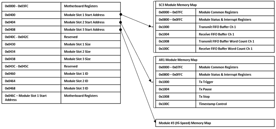
The memory map for the modules are dependent on the types of modules on the board and the order in which the modules are installed on the board as well as the firmware installed on the motherboard. The function modules are enumerated allowing for dynamic memory space allocation and therefore the “start” address of the module function register area is factory pre-defined (and read from) the Module Address register. Refer to Figure 1 for an example.
.68G6 Register Memory Map Addressing
Address Calculation
Motherboard Registers
Read/Write access to the motherboard registers starts with the base address for the board and then the motherboard base offset address.
For example, to address Module Slot 1 Start Address register (i.e. register address = 0x0400):
- Start with the base address for the board.
- Add the motherboard register address offset.
| Motherboard Address = | Base Address Motherboard Address Offset | = 0x9000 0400 |
| 0x9000 0000 + 0x0400 |
Module Registers:
Read/Write access to the Function module’s registers start with the base address of the board. Add the “content” for the Module Start Address and then, add the specific module function register offset.
For example, to address an appropriate/specific function module with a register offset:
- Start with the base address for the board.
- Add the value (contents) from the module base address offset register (contents/value of Motherboard Memory register for Module 1 (i.e., @ 0x0400) = 0x4000.
- Then add the specific module function Register Offset of interest (i.e., A/D Reading Ch 1 @ 0x1000)
| (Function Specific) Address = | Base Address + | Module Base Address Offset + | Function Register Offset | = 0x9000 5000 |
| 0x9000 0000 | 0x4000 | 0x1000 |
REGISTER DESCRIPTIONS
The register descriptions provide the Register Name, Type, Data Range, Read or Write information, power on default initialized values, a description of the function and a data table where applicable.
Module Information Registers
The Module Slot Addressing Ready, Module Slot Address, Module Slot Size and Module Slot ID registers provide information about the modules detected on the board.
Module Slot Addressing Ready
Link to original
Function: Indicates that the module slots are ready to be addressed. Type: unsigned binary word (32-bit) Data Range: 0x0000 0000 to 0xFFFF FFFF Read/Write: R Initialized Value: 0xA5A5A5A5 Operational Settings: This register will contain the value of 0xA5A5A5A5 when the module addresses have been determined.
Link to original
Module Slot Address Function: Specifies the Base Address for the module in the specific slot position. Type: unsigned binary word (32-bit) Data Range: 0x0000 0000 to 0xFFFF FFFF Read/Write: R Initialized Value: Based on board's module configuration. Operational Settings: 0x0000 0000 indicates no Module found.
Link to original
Module Slot Size Function: Specifies the Memory Size (in bytes) allocated for the module in the specific slot position. Type: unsigned binary word (32-bit) Range: 0x0000 0000 to 0xFFFF FFFF Read/Write: R Initialized Value: Assigned by factory for the module. Operational Settings: 0x0000 0000 indicates no Module found.
Module Slot ID Function: Specifies the Model ID for the module in the specified slot position. Type: 4-character ASCII string Data Range: 0x0000 0000 to 0xFFFF FFFF Read/Write: R Initialized Value: Assigned by factory for the module. Operational Settings: The Module ID is formatted as four ASCII bytes: three characters followed by a space. Module IDs are in little-endian order with a single space following the first three characters. For example, 'TL1' is '1LT', 'SC1' is '1CS' and so forth. Example below is for “TL1” (MSB justified). All value of 0000 0000 indicates no Module found. Link to original
D31 D30 D29 D28 D27 D26 D25 D24 D23 D22 D21 D20 D19 D18 D17 D16 ASCII Character (ex: 'T' - 0x54) ASCII Character (ex: 'L' - 0x4C) D15 D14 D13 D12 D11 D10 D9 D8 D7 D6 D5 D4 D3 D2 D1 D0 ASCII Character (ex: '1' - 0x31) ASCII Space (' ' - 0x20)
Hardware Information Registers
The registers identified in this section provide information about the board’s hardware.
Link to original
Product Serial Number Function: Specifies the Board Serial Number. Type: unsigned binary word (32-bit) Data Range: 0x0000 0000 to 0xFFFF FFFF Read/Write: R Initialized Value: Serial number assigned by factory for the board. Operational Settings: N/A
Platform
| Function: | Specifies the Board Platform Identifier. Values are for the ASCII characters for the NAI valid platforms (Identifiers). |
|---|---|
| Type: | unsigned binary word (32-bit) |
| Data Range: | See table below. |
| Read/Write: | R |
| Initialized Value: | ASCII code is for the Platform Identifier of the board |
| Operational Settings: | Valid NAI platform and the associated value for the platform is shown below: |
| NAI Platform | Platform Identifier | ASCII Binary Values (Note: little-endian order of ascii values) |
|---|---|---|
| 3U VPX | 68 | 0x0000 3836 |
Model
| Function: | Specifies the Board Model Identifier. Value is for the ASCII characters for the NAI valid model. |
|---|---|
| Type: | unsigned binary word (32-bit) |
| Data Range: | See table below. |
| Read/Write: | R |
| Initialized Value: | ASCII code is for the Model Identifier of the board |
| Operational Settings: | Example of NAI model and the associated value for the model is shown below: |
| NAI Model | ASCII Binary Values (Note: little-endian order of ascii values) |
|---|---|
| G | 0x0000 0047 |
Generation
| Function: | Specifies the Board Generation. Identifier values are for the ASCII characters for the NAI valid generation identifiers. |
|---|---|
| Type: | unsigned binary word (32-bit) |
| Data Range: | See table below. |
| Read/Write: | R |
| Initialized Value: | ASCII code is for the Generation Identifier of the board |
| Operational Settings: | Example of NAI generation and the associated value for the generation is shown below: |
| NAI Generation | ASCII Binary Values (Note: little-endian order of ascii values) |
|---|---|
| 6 | 0x0000 0036 |
Processor Count/Ethernet Count
| Function: | Specifies the Processor Count and Ethernet Count |
|---|---|
| Type: | unsigned binary word (32-bit) |
| Data Range: | See table below. |
| Read/Write: | R |
| Operational Settings: | Processor Count - Integer: indicates the number of unique processor types on the motherboard. + Ethernet Interface Count - Indicates the number of Ethernet interfaces on the product motherboard. For example, Single Ethernet = 1; Dual Ethernet = 2. |
| NAI Board | Processor Count | Description | |
| 3U-VPX | 68G6 | 1 | Xilinx Zynq UltraScale+ |
| D31 | D30 | D29 | D28 | D27 | D26 | D25 | D24 | D23 | D22 | D21 | D20 | D19 | D18 | D17 | D16 |
| Processor Count (See Table) | |||||||||||||||
| D15 | D14 | D13 | D12 | D11 | D10 | D9 | D8 | D7 | D6 | D5 | D4 | D3 | D2 | D1 | D0 |
| Ethernet Count (Based on Part Number Ethernet Options) | |||||||||||||||
Maximum Module Slot Count/ARM Platform Type
| Function: | Specifies the Maximum Module Slot Count and ARM Platform Type. |
|---|---|
| Type: | unsigned binary word (32-bit) |
| Data Range: | See table below. |
| Read/Write: | R |
| Operational Settings: | Maximum Module Slot Count - Indicates the number of modules that can be installed on the product. + ARM Platform - Altera = 1; Xilinx X1 = 2; Xilinx X2 = 3; UltraScale = 4 |
| NAI Board | Maximum Module Slot Count | ARM Platform Type | |
| 3U-VPX | 68G6 | 3 | UltraScale = 4 |
| D31 | D30 | D29 | D28 | D27 | D26 | D25 | D24 | D23 | D22 | D21 | D20 | D19 | D18 | D17 | D16 |
| Maximum Module Slot Count (See Table) | |||||||||||||||
| D15 | D14 | D13 | D12 | D11 | D10 | D9 | D8 | D7 | D6 | D5 | D4 | D3 | D2 | D1 | D0 |
| ARM Platform Type (See Table) | |||||||||||||||
Processor Operating System Registers
The registers in this section provide information about the Operating System that is running on the host processor on the motherboard. For boards that have more than one processor (ex. 75PPC1, 75INT2, 68PPC2, etc), the host processor would be the Power-PC or Intel processor.
ARM Processor Platform
Function: Specifies the ARM Processor on the motherboard. Values are for the ASCII characters for the NAI host processor platforms specified by the Operating System. Type: 8-character ASCII string - Two (2) unsigned binary word (32-bit) Data Range: N/A Read/Write: R Initialized Value: ASCII code is for the Host Platform Identifier of the board. Operational Settings: Valid NAI platforms based on Operating System loaded to host processor. Link to original
Processor Platform (Note: 8-character ASCII string) (“aarch64”) Word 1 (0x6372 6161 = “craa”) D31 D30 D29 D28 D27 D26 D25 D24 D23 D22 D21 D20 D19 D18 D17 D16 'c' (0x63) 'r' (0x72) D15 D14 D13 D12 D11 D10 D9 D8 D7 D6 D5 D4 D3 D2 D1 D0 'a' (0x61) 'a' (0x61) Word 2 (0x0034 3668 = “ 46h”) D31 D30 D29 D28 D27 D26 D25 D24 D23 D22 D21 D20 D19 D18 D17 D16 null (0x00) '4' (0x34) D15 D14 D13 D12 D11 D10 D9 D8 D7 D6 D5 D4 D3 D2 D1 D0 '6' (0x36) 'h' (0x68)
Processor Operating System
Function: Specifies the Operating System installed for the host processor. Values are for the ASCII characters for the NAI supported operating systems. Type: 12-character ASCII string - Three (3) unsigned binary word (32-bit) Data Range: N/A Read/Write: R Operational Settings: ASCII, 12 characters; ('Linux', 'VxWorks', 'RTOS', ...) Link to original
Processor Platform (Note: 12-character ASCII string) (“Linux”) Word 1 (0x756E 694C = “uniL”) D31 D30 D29 D28 D27 D26 D25 D24 D23 D22 D21 D20 D19 D18 D17 D16 'u' (0x75) 'n' (0x6E) D15 D14 D13 D12 D11 D10 D9 D8 D7 D6 D5 D4 D3 D2 D1 D0 'i' (0x69) 'L' (0x4C) Word 2 (0x0000 0078 = “ x”) D31 D30 D29 D28 D27 D26 D25 D24 D23 D22 D21 D20 D19 D18 D17 D16 null (0x00) null (0x00) D15 D14 D13 D12 D11 D10 D9 D8 D7 D6 D5 D4 D3 D2 D1 D0 null (0x00) null (0x00) Word 3 (0x0000 0000 = “ ”) D31 D30 D29 D28 D27 D26 D25 D24 D23 D22 D21 D20 D19 D18 D17 D16 null (0x00) null (0x00) D15 D14 D13 D12 D11 D10 D9 D8 D7 D6 D5 D4 D3 D2 D1 D0 null (0x00) null (0x00)
Processor Operating System Version
Function: Specifies the Version of Operating System installed for the host processor. Type: 8-character ASCII string - Two (2) unsigned binary word (32-bit) Data Range: N/A Read/Write: R Operational Settings: ASCII, 8 characters Link to original
Processor OS Version (Note: little-endian order of ascii values) (ex. “4.14.0”) Word 1 (Ex. 0x3431 2E34 = “41.4”) D31 D30 D29 D28 D27 D26 D25 D24 D23 D22 D21 D20 D19 D18 D17 D16 ex: '4' (0x34) ex: '1' (0x31) D15 D14 D13 D12 D11 D10 D9 D8 D7 D6 D5 D4 D3 D2 D1 D0 ex: '.' (0x2E) ex: '3' (0x33) Word 2 (Ex.0x 0000 302E = “ 0.”) D31 D30 D29 D28 D27 D26 D25 D24 D23 D22 D21 D20 D19 D18 D17 D16 null (0x00) null (0x00) D15 D14 D13 D12 D11 D10 D9 D8 D7 D6 D5 D4 D3 D2 D1 D0 ex: '0' (0x30) ex: '.' (0x2E)
Motherboard Firmware Information Registers
The registers in this section provide information on the revision of the firmware installed on the motherboard.
Transclude of Mb-Fpga-Firmware-Version-67Ppc2
Motherboard Firmware Build Time/Date
Function: Specifies the Build Date/Time of the NAI factory provided Motherboard Core Application installed on the board. Type: Two (2) unsigned binary word (32-bit) Data Range: N/A Read/Write: R Operational Settings: The motherboard firmware time consists of the Build Date and Build Time.
NOTE: On some builds the the Date/Time fields are fixed to 0000 0000 to maintain binary consistency across builds.Link to original
Motherboard Firmware Build Time (Note: little-endian order in register) Word 1 - Build Date (ex. 0x0E05 07E5 = 2021-5-14) D31 D30 D29 D28 D27 D26 D25 D24 D23 D22 D21 D20 D19 D18 D17 D16 Day (ex: 0x0E = 14) Month (ex: 0x05 = 5) D15 D14 D13 D12 D11 D10 D9 D8 D7 D6 D5 D4 D3 D2 D1 D0 Year (ex: 0x07E5 = 2021) Word 2 - Build Time (ex. 0x0005 3712 = 18:55:05) D31 D30 D29 D28 D27 D26 D25 D24 D23 D22 D21 D20 D19 D18 D17 D16 null (0x00) Seconds (ex: 0x05 = 05) D15 D14 D13 D12 D11 D10 D9 D8 D7 D6 D5 D4 D3 D2 D1 D0 Minutes (ex: 0x37 = 55) Hours (ex: 0x12 = 18)
Motherboard FPGA Compile Date/Time
Function: Specifies the Compile Date/Time of the NAI factory provided Motherboard FPGA installed on the board. Type: unsigned binary word (32-bit) Data Range: N/A Read/Write: R Operational Settings: The motherboard firmware time consists of the Build Date and Time in the following format: .
Link to original
Motherboard FPGA Compile Time (ex. 0xD22B 1809 = 04/26/21 17:32:09) D31 D30 D29 D28 D27 D26 D25 D24 D23 D22 D21 D20 D19 D18 D17 D16 Day (D31:D27) Month (D26:D23) Year (D22:D17) ex. 0xD ex. 0x2 0x2 0xB Day = 0x1A = 26 Month = 0x4 = 4 Year = 0x15 = 21 D15 D14 D13 D12 D11 D10 D9 D8 D7 D6 D5 D4 D3 D2 D1 D0 Hour (D16:D12) Minutes (D11:D6) Seconds (D5:D0) ex. 0x1 ex. 0x8 ex. 0x0 ex. 0x9 0 0 0 1 1 0 0 0 0 0 0 0 1 0 0 1 Hour = 0x11 = 17 Minutes = 0x20 = 32 Seconds = 0x09 = 09
Motherboard Monitoring Registers
The registers in this provide motherboard voltage and temperature measurement information.
Temperature Readings Register
The temperature registers provide the current, maximum (from power-up) and minimum (from power-up) for the processor and PCB for UltraScale processor.
These registers are only available on Xilinx Generation 5 platforms, and are periodically populated by the motherboard core application, which only runs in Petalinux and BareMetal. For other operating systems, refer to the naibrd Software Support Kit (SSK) naibsp_system_Monitor_Temperature_Get() routine to manually retrieve the temperature (NOTE: this feature is typically utilized for development/factory use only; contact the factory for additional details on potential use, if required).
Function: Specifies the Measured Temperatures on Motherboard. Type: signed byte (8-bits) for each temperature reading - Six (6) 32-bit words Data Range: 0x0000 0000 to 0xFFFF 0000 Read/Write: R Initialized Value: Value corresponding to the measured temperatures based on the table below. Operational Settings: The 8-bit temperature readings are signed bytes. For example, if the following register contains the value 0x2B2B 0000: Example:
Word 1 (UltraScale Temperatures) D31 D30 D29 D28 D27 D26 D25 D24 D23 D22 D21 D20 D19 D18 D17 D16 UltraScale Core Temperature UltraScale PCB Temperature D15 D14 D13 D12 D11 D10 D9 D8 D7 D6 D5 D4 D3 D2 D1 D0 0x00 0x00 The values would represent the following temperatures:
Temperature Measurements Data Bits Value Temperature (Celsius) UltraScale Core Temperature D31:D24 0x2B +43° UltraScale PCB Temperature D23:D16 0x2B +43° Link to original
Temperature Readings Word 1 (UltraScale Temperatures) D31 D30 D29 D28 D27 D26 D25 D24 D23 D22 D21 D20 D19 D18 D17 D16 UltraScale Core Temperature UltraScale PCB Temperature D15 D14 D13 D12 D11 D10 D9 D8 D7 D6 D5 D4 D3 D2 D1 D0 0x00 0x00 Word 2 (Reserved) D31 D30 D29 D28 D27 D26 D25 D24 D23 D22 D21 D20 D19 D18 D17 D16 0x00 0x00 D15 D14 D13 D12 D11 D10 D9 D8 D7 D6 D5 D4 D3 D2 D1 D0 0x00 0x00 Word 3 (Max UltraScale Temperatures) D31 D30 D29 D28 D27 D26 D25 D24 D23 D22 D21 D20 D19 D18 D17 D16 Max UltraScale Core Temperature Max UltraScale PCB Temperature D15 D14 D13 D12 D11 D10 D9 D8 D7 D6 D5 D4 D3 D2 D1 D0 0x00 0x00 Word 4 (Reserved) D31 D30 D29 D28 D27 D26 D25 D24 D23 D22 D21 D20 D19 D18 D17 D16 0x00 0x00 D15 D14 D13 D12 D11 D10 D9 D8 D7 D6 D5 D4 D3 D2 D1 D0 0 0 0 0 0 0 0 0 0 0 0 0 0 0 0 0 Word 5 (Min UltraScale Temperatures) D31 D30 D29 D28 D27 D26 D25 D24 D23 D22 D21 D20 D19 D18 D17 D16 Min UltraScale Core Temperature Min UltraScale PCB Temperature D15 D14 D13 D12 D11 D10 D9 D8 D7 D6 D5 D4 D3 D2 D1 D0 0 0 0 0 0 0 0 0 0 0 0 0 0 0 0 0 Word 6 (Reserved) D31 D30 D29 D28 D27 D26 D25 D24 D23 D22 D21 D20 D19 D18 D17 D16 0x00 0x00 D15 D14 D13 D12 D11 D10 D9 D8 D7 D6 D5 D4 D3 D2 D1 D0 0 0 0 0 0 0 0 0 0 0 0 0 0 0 0 00
Higher Precision Temperature Readings Registers
These registers provide higher precision readings of the current UltraScale Core and PCB temperatures.
Higher Precision UltraScale Core Temperature
Function: Specifies the Higher Precision Measured UltraScale Core temperature on Motherboard Board. Type: signed word (16-bits) for integer part and unsigned word (16-bits) for fractional part Data Range: 0x0000 0000 to 0xFFFF FFFF Read/Write: R Initialized Value: Measured UltraScale Core temperature on Motherboard Board Operational Settings: The upper 16-bits represent the signed integer part of the temperature, and the lower 16-bits represent the fractional part of the temperature with the resolution of 1/1000 of degree Celsius. For example, if the register contains the value 0x002B 0271, this represents UltraScale Core Temperature = 43.625° Celsius, and value 0xFFF6 0177 represents -10.375° Celsius. Link to original
D31 D30 D29 D28 D27 D26 D25 D24 D23 D22 D21 D20 D19 D18 D17 D16 Signed Integer Part of Temperature D15 D14 D13 D12 D11 D10 D9 D8 D7 D6 D5 D4 D3 D2 D1 D0 Fractional Part of Temperature
Higher Precision Motherboard PCB Temperature Function: Specifies the Higher Precision Measured Motherboard PCB temperature. Type: signed word (16-bits) for integer part and unsigned word (16-bits) for fractional part Data Range: 0x0000 0000 to 0xFFFF FFFF Read/Write: R Initialized Value: Measured Motherboard PCB temperature Operational Settings: The upper 16-bits represent the signed integer part of the temperature and the lower 16-bits represent the fractional part of the temperature with the resolution of 1/1000 of degree Celsius. For example, if the register contains the value 0x0020 007D, this represents Interface PCB Temperature = 32.125° Celsius, and value 0xFFE8 036B represents -24.875° Celsius. Link to original
D31 D30 D29 D28 D27 D26 D25 D24 D23 D22 D21 D20 D19 D18 D17 D16 Signed Integer Part of Temperature D15 D14 D13 D12 D11 D10 D9 D8 D7 D6 D5 D4 D3 D2 D1 D0 Fractional Part of Temperature
Motherboard Health Monitoring Registers
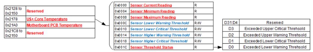
The registers in this section provide a summary of motherboard temperature sensors and their corresponding bits. Additionally, this section provides an overview of the registers allocated to those sensors, which are used to monitor current/minimum/maximum temperature readings, upper & lower critical/warning temperature thresholds, and whether or not a programmed temperature threshold has been exceeded.
These registers are only available on Xilinx Generation 5 platforms, and are periodically populated by the motherboard core application, which only runs in Petalinux and BareMetal. For other operating systems, refer to the naibrd Software Support Kit (SSK) naibsp_system_Monitor_Temperature_Get() routine to manually retrieve the temperature (NOTE: this feature is typically utilized for development/factory use only; contact the factory for additional details on potential use, if required).
Transclude of Sensor-Summary-Status-Us
Motherboard Sensor Registers
The registers listed in this section apply to each module sensor listed for the Motherboard Sensor Summary Status register.
Transclude of Mb-Sensor-Registers-Us
Sensor Threshold Status Function: Reflects which threshold has been crossed Type: unsigned binary word (32-bits) Data Range: See table below Read/Write: R Initialized Value: 0 Operational Settings: The associated bit is set when the sensor reading exceed the corresponding threshold settings. Link to original
Bit(s) Description D31:D4 Reserved D3 Exceeded Upper Critical Threshold D2 Exceeded Upper Warning Threshold D1 Exceeded Lower Critical Threshold D0 Exceeded Lower Warning Threshold
Link to original
Sensor Current Reading Function: Reflects current reading of temperature sensor Type: Single Precision Floating Point Value (IEEE-754) Data Range: Single Precision Floating Point Value (IEEE-754) Read/Write: R Initialized Value: N/A Operational Settings: The register represents current sensor reading as a single precision floating point value. For example, for a temperature sensor, register value 0x41C6 0000 represents temperature = 24.75° Celsius.
Link to original
Sensor Minimum Reading Function: Reflects minimum value of temperature sensor since power up Type: Single Precision Floating Point Value (IEEE-754) Data Range: Single Precision Floating Point Value (IEEE-754) Read/Write: R Initialized Value: N/A Operational Settings: The register represents minimum sensor value as a single precision floating point value. For example, for a temperature sensor, register value 0x41C6 0000 represents temperature = 24.75° Celsius.
Link to original
Sensor Maximum Reading Function: Reflects maximum value of temperature sensor since power up Type: Single Precision Floating Point Value (IEEE-754) Data Range: Single Precision Floating Point Value (IEEE-754) Read/Write: R Initialized Value: N/A Operational Settings: The register represents maximum sensor value as a single precision floating point value. For example, for a temperature sensor, register value 0x41C6 0000 represents temperature = 24.75° Celsius.
Link to original
Sensor Lower Warning Threshold Function: Reflects lower warning threshold of temperature sensor Type: Single Precision Floating Point Value (IEEE-754) Data Range: Single Precision Floating Point Value (IEEE-754) Read/Write: R/W Initialized Value: Default lower warning threshold (value dependent on specific sensor) Operational Settings: The register represents sensor lower warning threshold as a single precision floating point value. For example, for a temperature sensor, register value 0xC220 0000 represents temperature = -40.0° Celsius.
Link to original
Sensor Lower Critical Threshold Function: Reflects lower critical threshold of temperature sensor Type: Single Precision Floating Point Value (IEEE-754) Data Range: Single Precision Floating Point Value (IEEE-754) Read/Write: R/W Initialized Value: Default lower critical threshold (value dependent on specific sensor) Operational Settings: The register represents sensor lower critical threshold as a single precision floating point value. For example, for a temperature sensor, register value 0xC25C 0000 represents temperature = -55.0° Celsius.
Link to original
Sensor Upper Warning Threshold Function: Reflects upper warning threshold of temperature sensor Type: Single Precision Floating Point Value (IEEE-754) Data Range: Single Precision Floating Point Value (IEEE-754) Read/Write: R/W Initialized Value: Default upper warning threshold (value dependent on specific sensor) Operational Settings: The register represents sensor upper warning threshold as a single precision floating point value. For example, for a temperature sensor, register value 0x42AA 0000 represents temperature = 85.0° Celsius.
Link to original
Sensor Upper Critical Threshold Function: Reflects upper critical threshold of temperature sensor Type: Single Precision Floating Point Value (IEEE-754) Data Range: Single Precision Floating Point Value (IEEE-754) Read/Write: R/W Initialized Value: Default upper critical threshold (value dependent on specific sensor) Operational Settings: The register represents sensor upper critical threshold as a single precision floating point value. For example, for a temperature sensor, register value 0x42FA 0000 represents temperature = 125.0° Celsius.
Ethernet Configuration Registers
The registers in this section provide information about the Ethernet Configuration for the two ports on the board.
Important: Regardless if the board is configured for one or two Ethernet ports, the second IP address cannot be on the same Subnet as the First IP Address. The table below provides examples of valid and invalid IP Addresses and Subnet Mask Addresses.
Link to original
First Port (A) IP Address First Port (A) Subnet Mask Second Port (B) IP Address Second Port (B) Subnet Mask Result 192.168.1.5 255.255.255.0 192.168.2.5 255.255.255.0 Good 192.168.1.5 255.255.0.0 192.168.2.5 255.255.0.0 Conflict 192.168.1.5 255.255.0.0 192.168.2.5 255.255.255.0 Conflict 10.0.0.15 255.0.0.0 192.168.1.5 255.255.255.0 Good
Ethernet MAC Address and Ethernet Settings Function: Specifies the Ethernet MAC Address and Ethernet Settings for the Ethernet port. Type: Two (2) unsigned binary word (32-bit) Data Range: See table. Read/Write: R Operational Settings: The Ethernet MAC Address consists of six octets. The Ethernet Settings are defined in table.
Bits Description Values D31:D23 Reserved 0 D22:D21 Duplex 00 = Not Specified, ` 01 = Half Duplex, ` 10 = Full Duplex, + 11 = Reserved D20:D18 Speed 000 = Not Specified, ` 001 = 10 Mbps, ` 010 = 100 Mbps, ` 011 = 1000 Mbps, ` 100 = 2500 Mbps, ` 101 = 10000 Mbps, ` 110 = Reserved, + 111 = Reserved D17 Auto Negotiate 0 = Enabled, + 1 = Disabled D16 Static IP Address 0 = Enabled, + 1 = Disabled Link to original
Ethernet MAC Address and Ethernet Settings (Note: little-endian order in register) Word 1 (Ethernet MAC Address (Octets 1-4)) (ex: aa:bb:cc:dd:ee:ff) D31 D30 D29 D28 D27 D26 D25 D24 D23 D22 D21 D20 D19 D18 D17 D16 MAC Address Octet 4 (ex: 0xDD) MAC Address Octet 3 (ex: 0xCC) D15 D14 D13 D12 D11 D10 D9 D8 D7 D6 D5 D4 D3 D2 D1 D0 MAC Address Octet 2 (ex: 0xBB) MAC Address Octet 1 (ex: 0xAA) Word 2 (Ethernet MAC Address (Octets 5-6) and Ethernet Settings) D31 D30 D29 D28 D27 D26 D25 D24 D23 D22 D21 D20 D19 D18 D17 D16 Ethernet Settings (See table) D15 D14 D13 D12 D11 D10 D9 D8 D7 D6 D5 D4 D3 D2 D1 D0 MAC Address Octet 6 (ex: 0xFF) MAC Address Octet 5 (ex: 0xEE)
Ethernet Interface Name Function: Specifies the Ethernet Interface Name for the Ethernet port. Type: 8-character ASCII string Data Range: See table. Read/Write: R Operational Settings: The Ethernet Interface Name (eth0, eth1, etc) for the Ethernet port. Link to original
Ethernet Interface Name (Note: ascii string in register) (ex. “eth0”) Word 1 (Bit 0-31) (ex: 0x3068 7465 = “0hte”) D31 D30 D29 D28 D27 D26 D25 D24 D23 D22 D21 D20 D19 D18 D17 D16 ASCII Character (ex: '0' - 0x30) ASCII Character (ex: 'h' - 0x68) D15 D14 D13 D12 D11 D10 D9 D8 D7 D6 D5 D4 D3 D2 D1 D0 ASCII Character (ex: 't' - 0x74) ASCII Character (ex: 'e' - 0x65) Word 2 (Bit 32-63) (ex: 0x0000 0000) D31 D30 D29 D28 D27 D26 D25 D24 D23 D22 D21 D20 D19 D18 D17 D16 ASCII Character (ex: null - 0x00) ASCII Character (ex: null - 0x00) D15 D14 D13 D12 D11 D10 D9 D8 D7 D6 D5 D4 D3 D2 D1 D0 ASCII Character (ex: null - 0x00) ASCII Character (ex: null - 0x00)
Ethernet IPv4 Address Function: Specifies the Ethernet IPv4 Address for the Ethernet port. Type: Three (3) unsigned binary word (32-bit) Data Range: See table. Read/Write: R Operational Settings: The Ethernet IPv4 Address consists of three parts: IPv4 Address, IPv4 Subnet Mask and IPv4 Gateway. Link to original
Ethernet IPv4 Address (Note: little-endian order in register) Word 1 (Ethernet IPv4 Address) (ex: 0x1001 A8C0 = 192.168.1.16) D31 D30 D29 D28 D27 D26 D25 D24 D23 D22 D21 D20 D19 D18 D17 D16 IPv4 Address Octet 4 (ex: 0x10 = 16) IPv4 Address Octet 3 (ex: 0x01 = 1) D15 D14 D13 D12 D11 D10 D9 D8 D7 D6 D5 D4 D3 D2 D1 D0 IPv4 Address Octet 2 (ex: 0xA8 = 168) IPv4 Address Octet 1 (ex: 0xC0 = 192) Word 2 (Ethernet IPv4 Subnet) (ex: 0x00FF FFFF = 255.255.255.0) D31 D30 D29 D28 D27 D26 D25 D24 D23 D22 D21 D20 D19 D18 D17 D16 IPv4 Subnet Octet 4 (ex: 0x00 = 0) IPv4 Subnet Octet 3 (ex: 0xFF = 255) D15 D14 D13 D12 D11 D10 D9 D8 D7 D6 D5 D4 D3 D2 D1 D0 IPv4 Subnet Octet 2 (ex: 0xFF = 255) IPv4 Subnet Octet 1 (ex: 0xFF = 255) Word 3 (Ethernet IPv4 Gateway) (ex: 0x0101 A8C0 = 192.168.1.1) D31 D30 D29 D28 D27 D26 D25 D24 D23 D22 D21 D20 D19 D18 D17 D16 IPv4 Gateway Octet 4 (ex: 0x01 = 1) IPv4 Gateway Octet 3 (ex: 0x01 = 1) D15 D14 D13 D12 D11 D10 D9 D8 D7 D6 D5 D4 D3 D2 D1 D0 IPv4 Gateway Octet 2 (ex: 0xA8 = 168) IPv4 Gateway Octet 1 (ex: 0xC0 = 192)
Ethernet IPv6 Address Function: Specifies the Ethernet IPv6 Address for the Ethernet port. Type: Five (5) unsigned binary word (32-bit) Data Range: See table. Read/Write: R Operational Settings: The IPv6 Prefix length indicates the network portion of an IPv6 address using the following format: IPv6 address/prefix length ` Prefix length can range from 0 to 128 ` * Typical prefix length is 64 The following is an illustration of IPv6 addressing with IPv6 Prefix length of 64.
64 bits 64 bits Prefix Interface ID Prefix 1 Prefix 2 Prefix 3 Subnet ID Interface ID 1 Interface ID 2 Interface ID 3 Interface ID 4 Example: 2002:c0a8:101:0:7c99:d118:9058:1235/64 2002 C0A8 0101 0000 7C99 D118 9058 1235 Link to original
Ethernet IPv6 Address (Note: little-endian order within 32-bit and 16-bit words in register) (ex. IPv6 Address: 2002:c0a8:201:0:7c99:d118:9058:1235 IPv6 Prefix: 64) Word 1 (Ethernet IPv6 Address (Prefix 1-2)) (ex:0xA8C0 0220 = 2002 C0A8) D31 D30 D29 D28 D27 D26 D25 D24 D23 D22 D21 D20 D19 D18 D17 D16 Prefix 2 (ex: 0xA8C0 = C0A8) D15 D14 D13 D12 D11 D10 D9 D8 D7 D6 D5 D4 D3 D2 D1 D0 Prefix 1 (ex: 0x0220 = 2002) Word 2 (Ethernet IPv6 Address (Prefix 3/Subnet ID)) + (ex:0x000 0101 = 0101 0000) D31 D30 D29 D28 D27 D26 D25 D24 D23 D22 D21 D20 D19 D18 D17 D16 Subnet ID (ex: 0x0000 = 0000) D15 D14 D13 D12 D11 D10 D9 D8 D7 D6 D5 D4 D3 D2 D1 D0 Prefix 3 (ex: 0x0101 = 0101) Word 3 (Ethernet IPv6 Address (Interface ID 1-2)) + (ex: 0x18D1 997C = 7C99 D118) D31 D30 D29 D28 D27 D26 D25 D24 D23 D22 D21 D20 D19 D18 D17 D16 Interface ID 2 (ex: 0x18D1 = D118) D15 D14 D13 D12 D11 D10 D9 D8 D7 D6 D5 D4 D3 D2 D1 D0 Interface ID 1 (ex: 0x997C = 7C99) Word 4 (Ethernet IPv6 Address (Interface ID 3-4)) + (ex: 0x3512 5890 = 9058 1235) D31 D30 D29 D28 D27 D26 D25 D24 D23 D22 D21 D20 D19 D18 D17 D16 Interface ID 4 (ex: 0x3512 = 1235) D15 D14 D13 D12 D11 D10 D9 D8 D7 D6 D5 D4 D3 D2 D1 D0 Interface ID 3 (ex: 0x5890 = 9058) Word 5 (Ethernet IPv6 Prefix Length) + (ex:0x0000 0040) D31 D30 D29 D28 D27 D26 D25 D24 D23 D22 D21 D20 D19 D18 D17 D16 0 0 0 0 0 0 0 0 0 0 0 0 0 0 0 0 D15 D14 D13 D12 D11 D10 D9 D8 D7 D6 D5 D4 D3 D2 D1 D0 Prefix Length (ex: 0x0040 = 64)
Interrupt Vector and Steering
When interrupts are enabled, the interrupt vector associated with the specific interrupt can be programmed (typically with a unique number/identifier) such that it can be utilized in the Interrupt Service Routine (ISR) to identify the type of interrupt. When an interrupt occurs, the contents of the Interrupt Vector registers is reported as part of the interrupt mechanism. In addition to specifying the interrupt vector, the interrupt can be directed (“steered”) to the native bus or to the application running on the onboard ARM processor.
Note
The Interrupt Vector and Interrupt Steering registers are mapped to the Motherboard Common Memory and these registers are associated with the Module Slot position (refer to Function Register Map).
Interrupt Vector Function: Set an identifier for the interrupt. Type: unsigned binary word (32-bit) Data Range: 0x0000 0000 to 0xFFFF FFFF Read/Write: R/W Initialized Value: 0 Operational Settings: When an interrupt occurs, this value is reported as part of the interrupt mechanism.
Interrupt Steering Function: Sets where to direct the interrupt. Type: unsigned binary word (32-bit) Data Range: See table Read/Write: R/W Initialized Value: 0 Operational Settings: When an interrupt occurs, the interrupt is sent as specified: Link to original
Direct Interrupt to VME 1 Direct Interrupt to ARM Processor (via SerDes) +
(Custom App on ARM or NAI Ethernet Listener App)2 Direct Interrupt to PCIe Bus 5 Direct Interrupt to cPCI Bus 6
Modules Health Monitoring
Module BIT Status Function: Provides the ability to monitor the individual Module BIT Status. Type: unsigned binary word (32-bit) Data Range: 0x0000 0000 to 0xFFFF FFFF Read/Write: R Operational Settings: The Module BIT Status registers provide the ability to monitor individual Module BIT results as Latched and current value. A 1 is any bit field indicates BIT failure for the Module in that slot. Link to original
Bit(s) Description D31:D20 Reserved D19 Module Slot 3 BIT Failure (current value) D18 Module Slot 2 BIT Failure (current value) D17 Module Slot 1 BIT Failure (current value) D16 Reserved D15:D4 Reserved D3 Module Slot 3 BIT Failure - Latched D2 Module Slot 2 BIT Failure - Latched D1 Module Slot 1 BIT Failure - Latched D0 Reserved
Scratchpad Area
Link to original
Scratchpad Area Function: Registers reserved as scratch pad for customer use. Type: unsigned binary word (32-bit) Data Range: 0x0000 0000 to 0xFFFF FFFF Read/Write: R/W Operational Settings: This area in memory is reserved for customer use.
MOTHERBOARD FUNCTION REGISTER MAP
Key:
| Bold Underline = | Measurement/Status/Board Information |
|---|---|
| Bold Italic = | Configuration/Control |
Motherboard Information Registers
| Addr (Hex) | Name | Read/Write |
|---|---|---|
| 0x03FC | Module Slot Addressing Ready | R |
| Addr (Hex) | Name | Read/Write |
|---|---|---|
| 0x0400 | Module Slot 1 Address | R |
| 0x0404 | Module Slot 2 Address | R |
| 0x0408 | Module Slot 3 Address | R |
| Addr (Hex) | Name | Read/Write |
|---|---|---|
| 0x0430 | Module Slot 1 Size | R |
| 0x0434 | Module Slot 2 Size | R |
| 0x0438 | Module Slot 3 Size | R |
| Addr (Hex) | Name | Read/Write |
|---|---|---|
| 0x0460 | Module Slot 1 ID | R |
| 0x0464 | Module Slot 2 ID | R |
| 0x0468 | Module Slot 3 ID | R |
Hardware Information Registers
| Addr (Hex) | Name | Read/Write |
|---|---|---|
| 0x0020 | Product Serial Number | R |
| Addr (Hex) | Name | Read/Write |
|---|---|---|
| 0x0024 | Platform | R |
| 0x0028 | Model | R |
| 0x002C | Generation | R |
| Addr (Hex) | Name | Read/Write |
|---|---|---|
| 0x0030 | Processor Count/Ethernet Count | R |
| 0x0034 | Maximum Module Slot Count/ARM Platform Type | R |
| Addr (Hex) | Name | Read/Write |
|---|---|---|
| 0x0038 | Processor Platform (Bit 0-31) | R |
| 0x003C | Processor Platform (Bit 32-63) | R |
| Addr (Hex) | Name | Read/Write |
|---|---|---|
| 0x0040 | Processor Operating System (Bit 0-31) | R |
| 0x0044 | Processor Operating System (Bit 32-63) | R |
| 0x0048 | Processor Operating System (Bit 64-95) | R |
| Addr (Hex) | Name | Read/Write |
|---|---|---|
| 0x004C | Processor Operating System Version (Bit 0-31) | R |
| 0x0050 | Processor Operating System Version (Bit 32-63) | R |
Motherboard Firmware Information Registers
Motherboard Core Information
| Addr (Hex) | Name | Read/Write |
|---|---|---|
| 0x0100 | MB Core Major/Minor Version | R |
| 0x0104 | MB Core Minor 2/3 Version | R |
| 0x0108 | MB Core Build Date (Bit 0-31) | R |
| 0x010C | MB Core Build Date (Bit 32-63) | R |
Motherboard FPGA Information
| Addr (Hex) | Name | Read/Write |
|---|---|---|
| 0x0270 | MB FPGA Revision | R |
| 0x0274 | MB FPGA Compile Date/Time | R |
Motherboard Monitoring Registers
Temperature Readings
| Addr (Hex) | Name | Read/Write |
|---|---|---|
| 0x0200 | Current UltraScale Temperatures | R |
| 0x0204 | Reserved | R |
| 0x0208 | Max UltraScale Temperatures | R |
| 0x020C | Reserved | R |
| 0x0210 | Min UltraScale Temperatures | R |
| 0x0214 | Reserved | R |
Higher Precision Temperature Readings
| Addr (Hex) | Name | Read/Write |
|---|---|---|
| 0x0230 | Current UltraScale Core Temperature | R |
| 0x0234 | Current UltraScale PCB Temperature | R |
Motherboard Health Monitoring Registers
| Addr (Hex) | Name | Read/Write |
|---|---|---|
| 0x20F8 | Motherboard Sensor Summary Status | R |
Ethernet Configuration Registers
| Addr (Hex) | Name | Read/Write |
|---|---|---|
| 0x0070 | Ethernet A MAC (Octets 1-4) | R |
| 0x0074 | Ethernet A MAC (Octets 5-6)/Misc Settings | R |
| Addr (Hex) | Name | Read/Write |
|---|---|---|
| 0x0078 | Ethernet A Interface Name (Bit 0-31) | R |
| 0x007C | Ethernet A Interface Name (Bit 32-63) | R |
| Addr (Hex) | Name | Read/Write |
|---|---|---|
| 0x0080 | Ethernet A IPv4 Address | R |
| 0x0084 | Ethernet A IPv4 Subnet Mask | R |
| 0x0088 | Ethernet A IPv4 Gateway | R |
| Addr (Hex) | Name | Read/Write |
|---|---|---|
| 0x008C | Ethernet A IPv6 Address (Prefix 1-2) | R |
| 0x0090 | Ethernet A IPv6 Address (Prefix 3/Subnet ID) | R |
| 0x0094 | Ethernet A IPv6 Address (Interface ID 1-2) | R |
| 0x0098 | Ethernet A IPv6 Address (Interface ID 3-4) | R |
| 0x009C | Ethernet A IPv6 Prefix Length | R |
| Addr (Hex) | Name | Read/Write |
|---|---|---|
| 0x00A0 | Ethernet B MAC (Octets 1-4) | R |
| 0x00A4 | Ethernet B MAC (Octets 5-6)/Misc Settings | R |
| Addr (Hex) | Name | Read/Write |
|---|---|---|
| 0x00A8 | Ethernet B Interface Name (Bit 0-31) | R |
| 0x00AC | Ethernet B Interface Name (Bit 32-63) | R |
| Addr (Hex) | Name | Read/Write |
|---|---|---|
| 0x00B0 | Ethernet B IPv4 Address | R |
| 0x00B4 | Ethernet B IPv4 Subnet Mask | R |
| 0x00B8 | Ethernet B IPv4 Gateway | R |
| Addr (Hex) | Name | Read/Write |
|---|---|---|
| 0x00BC | Ethernet B IPv6 Address (Prefix 1-2) | R |
| 0x00C0 | Ethernet B IPv6 Address (Prefix 3/Subnet ID) | R |
| 0x00C4 | Ethernet B IPv6 Address (Interface ID 1-2) | R |
| 0x00C8 | Ethernet B IPv6 Address (Interface ID 3-4) | R |
| 0x00CC | Ethernet B IPv6 Prefix Length | R |
Interrupt Vector and Steering
| Addr (Hex) | Name | Read/Write | Addr (Hex) | Name | Read/Write |
|---|---|---|---|---|---|
| 0x0500 - 0x057C | Module 1 Interrupt Vector 1-32 | R/W | 0x0600 - 0x067C | Module 1 Interrupt Steering 1-32 | R/W |
| 0x0700 - 0x077C | Module 2 Interrupt Vector 1-32 | R/W | 0x0800 - 0x087C | Module 2 Interrupt Steering 1-32 | R/W |
| 0x0900 - 0x097C | Module 3 Interrupt Vector 1-32 | R/W | 0x0A00 - 0x0A7C | Module 3 Interrupt Steering 1-32 | R/W |
Modules Health Monitoring
Module BIT Status
| Addr (Hex) | Name | Read/Write |
|---|---|---|
| 0x0128 | Module BIT Status (current and latched) | R |
Scratchpad Registers
| Addr (Hex) | Name | Read/Write |
|---|---|---|
| 0x3800 - 0x3BFF | Scratchpad Registers | R/W |
ETHERNET
(For detailed supplement, please visit the NAI web-site specific product page and refer to: Ethernet Interface for Generation 5 SBC and Embedded IO Boards Specification)
Note
For products capable of 10/100/1000Base-KX functionality - the product Ethernet PHY supports 1000BASE-X. Product interoperability with 10/100/1000BASE-KX is supported with 1000BASE-X (provided that auto-negotiation is disabled).
The Ethernet Interface Option allows communications and control access to all function modules either via the system BUS or Ethernet ports 1 or 2.
Ethernet 1 Ethernet 2 Ethernet 3* Ethernet 4* (REF PORT A) (REF PORT B) (REF PORT C) (REF PORT D) The default IP address: 192.168.1.16 192.168.2.16 192.168.3.16 192.168.4.16 The default subnet: 255.255.255.0 255.255.255.0 255.255.255.0 255.255.255.0 The default gateway: 192.168.1.1 192.168.2.1 192.168.3.1 192.168.4.1 *see Part Number Designation for applicability.
Note
Actual “as shipped” card Ethernet default IP addresses may vary based upon final ATP configuration(s).
The NAI interface supports IPv4 and IPv6 and both the TCP and UDP protocols. The Ethernet Operation Mode Command Listener application running on the motherboard host processor implements the operation interface. The listener is operational on startup through the nai_MBStartup process and listen on specific ports for commands to process. The default ports are listed below:
- TCP1 - Port 52801
- TCP2 - Port 52802
- UDP1 - Port 52801
- UDP2 - Port 52802
While the listener is active, note that interrupts from the motherboard do not trigger. The listener can be disabled by turning off the nai_MBStartup process through the Motherboard EEPROM. To turn off nai_MBStartup use the command mbeeprom_util set MBStartupInitOnlyFlag 1 in the console, either by serial port or telnet to the motherboard, and then reboot the system. To turn on the nai_MBStartup use the command mbeeprom_util set MBStartupInitOnlyFlag 0 in the console, either by serial port or telnet to the motherboard, and then reboot the system.
Ethernet Message Framework
The interface uses a specific message framework for all commands and responses. All messages begin with a Preamble code and end with a Postamble code. The message framework is shown below.
Preamble
2 bytes Always
0xD30FSequenceNo
2 bytesType Code
2 byteMessage Length
(2 bytes)Payload
(0..1414 bytes)Postamble
2 bytes
Always
0xF03DMessage Elements
Preamble The Preamble is used to delineate the beginning of a message frame.
The Preamble is always 0xD30F.SequenceNo The SequenceNo is used to associate Commands with Responses. Type Code Type Codes are used to define the type of Command or Response the message contains. Message Length The Message Length is the number of bytes in the complete message frame starting with and including the
Preamble and ending with and including the Postamble.Payload The Payload contains the unique data that makes up the command or response.
Payloads vary based on command type.Postamble The Postamble is use to delineate the end of a message frame.
The Postamble is always 0xF03D.Notes
- The messaging protocol applies only to card products.
- Messaging is managed by the connected (client) computer. The client computer will send a single message and wait for a reply from the card. Multiple cards may be managed from a single computer, subject to channel and computer capacity.
Board Addressing
The interface provides two main addressing areas: Onboard and Off-board.
Onboard addressing refers to accessing resources located on the board that is implementing the operation interface (including its modules).
Off-board addressing refers to accessing resources located on another board reachable via VME, PCI, or other bus. Off-board addressing requires a Master/Slave configuration.
The user must always specify if a particular address is Onboard or Off-board. See the command descriptions for the onboard and off-board flags.
Within a particular board (Onboard or Off-board), the address space is broken up into two areas: Motherboard Common Address Space and Module Address Space. All addresses are 32-bit.
Motherboard Common Address Space starts at 0x00000000 and ends at 0x00004000. This is a 4Kx32-bit address space (16 kbytes).
Module Address Space starts at 0x00004000. Module addressing is dynamically configured at startup. NAI boards support between 1 and 6 modules. The minimum module address space size is 4Kx32 (16 kbytes) and module sizes are always a multiple of 4Kx32.
Module addressing is dynamic and cumulative. The first detected module (starting with Slot 1) is given an address of 0x00004000. The 2nd detected Module is given an address of:
First_Detected_Module_Address + First_Detected_Module_Size
Note
Slots do not define addresses.
If no module is detected in a module slot, that slot is not given an address. Therefore, if the first detected Module is in Slot 2, then that module address will be 0x00004000. If the next detected module is in Slot 4, then the address of that Module will be:
Second_Detected_Module_Address = First_Detected_Module_Address + First_Detected_Module_Size
If a 3rd Module is detected in Slot 6, then the address of that Module will be:
Third_Detected_Module_Address = Second_Detected_Module_Address + Second_Detected_Module_Size
Note
Module addresses are calculated at each board startup when the modules are detected. Therefore, if a module should fail to be detected due to malfunction or because it was removed from the motherboard, the addresses of the modules that follow it in the slot sequence will be altered. This is important to note when programming to this interface.
Users can always retrieve the Module Addresses, Module Sizes and Module IDs from the fixed Motherboard Common address area. This data is set upon each board startup. While the Module Addressing is dynamic, the address where these addresses are stored is fixed. For example, to find the startup address of the module location in Slot 3, refer to the MB Common Address 0x00000408 from the Motherboard Common Addresses table that follows.
Ethernet Wiring Convention
Link to original
RJ-45 Pin T568A Color T568B Color 10/100Base-T 1000BASE-T NAI wiring convention 1 white/green stripe white/orange stripe TX+ DA+ ETH-TP0+ 2 green orange TX- DA- ETH-TP0- 3 white/orange stripe white/green stripe RX+ DB+ ETH-TP1+ 4 blue blue DC+ ETH-TP2+ 5 white/blue stripe white/blue stripe DC- ETH-TP2- 6 orange green RX- DB- ETH-TP1- 7 white/brown stripe white/brown stripe DD+ ETH-TP3+ 8 brown brown DD- ETH-TP3-
68G6 CONNECTOR/PIN-OUT INFORMATION
The 68G6 3U OpenVPX SOSA Aligned MFI/O-Intensive Processing Board is available in two configurations: convection-cooled and conduction-cooled. The 68G6 follows the OpenVPX “Payload Slot Profile” configured as:
| Slot profile: | SLT3-PAY-2U2U-14.2.17 |
|---|---|
| Module profile: | MODA3p-16.2.16-1-F2C-(P3U)(2E7) |
User I/O is available through the OpenVPX user defined rear I/O connectors P1, P2 (see part number and pin-out information).
Notes
Front Panel Connector
Utility Connector J5
Industry standard mini-HDMI type (type-C receptacle).
Panel LEDs
Front Panel LEDs indications (only available on air-cooled units).
| LED | ILLUMINATED | EXTINGUISHED |
| GRN: | Blinking: Initializing Steady On: Power-On / Ready | Power off |
| RED: | Module BIT error | No BIT fault |
| YEL: (flash) | Card access (bus or Gig-E activity) | No card activity |
Chassis Ground
Rear connector key guides are chassis ground
Front Panel Utility Connector J5 (Air and Conduction-Cooled)
The 68G6 utilizes a Mini-HDMI type card edge connector J5, available on either air or conduction-cooled configurations that provides the following signals:
- Serial (port 1)
- USB 2.0
- Ethernet port A
NAI also provides an optional “breakout” adapter board (NAI P/N 75SBC4-BB) with a mini-HDMI to mini-HDMI type cable. The “breakout” adapter board and a Micro-HDMI cable (NAI P/N 75SBC4-BB) allow for standard I/O connections to Ethernet and asynchronous serial (DB9). Consult the factory for availability
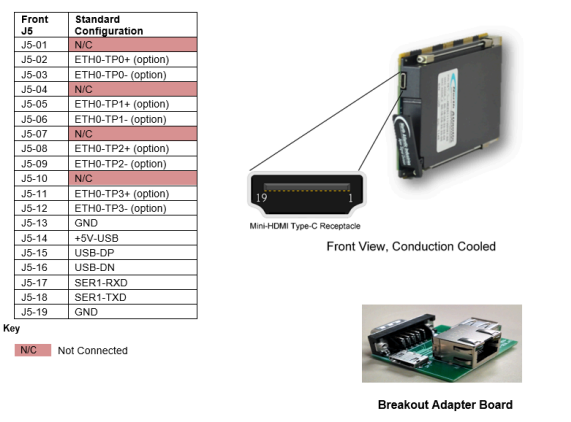
Signal Descriptions J5
| Signal Name | Description |
|---|---|
| ETH0-TPx | Ethernet port A signals (4 pair) 10/100/1000 twisted pair signals (Optional - available only if NOT re-directed to rear I/O (see part number configuration options) |
| USB-DP | Front Panel USB Data Positive |
| USB-DN | Front Panel USB Data Negative |
| SER1-TXD | Asynchronous transmit serial data port 1 (out) / RS232 debug/console port only |
| SER1-RXD | Asynchronous received serial data port 1 (in) / RS232 debug/console port only |
| GND | System Ground (return) |
Rear I/O VPX Connectors P0-P2 (Conduction-Cooled)
The 68G6 3U OpenVPX SOSA Aligned MFI/O-Intensive Processing Board provides interface via the rear VPX connectors.
Rear I/O Summary
Signals defined as N/C currently have no functionality associated and are not required for general operation.
| P0 - Utility plane. Contains the following signal definitions: | |
| Power: | Primary +12V, +3.3V_Aux, and System GND |
| Geographical Address Pins: | GA0# - GA4#, GAP# |
| Card reset: | SYSRST# signal |
| IPMC IMPB-SDA-A, | IMPB-SDA-B, IMPB-SCL-A, IMPB-SCL-B |
| VPX AUX/REF CLK | (Not used) |
| P1 - Defined as primarily Data/Control Planes (User defined I/O secondary) | |
| High Speed Switched Fabric Interface: | Two ultra-thin pipe options (PCIe ver. 3.0 (x1)). |
| Ethernet: | Dual Gig-E port option(s) are available and defined |
| (See Part Number Designation section) | |
| P2 - User defined I/O (primary) |
|---|
Rear I/O Utility Plane (P0)
The P0 (Utility) Plane contains the primary power, bus, and utility signals for the OpenVPX board. Additionally, several of the user defined pins can be utilized for Geographical Addressing and a parallel SYSRST# signal. Signals defined as N/C currently have no functionality associated and is not required for general operation.
| UTILITY | Row | Row | Row | Row | Row | Row | Row |
| P0 | G | F | E | D | C | B | A |
| 1 | (+)12V (VS1) | (+)12V (VS1) | (+)12V (VS1) | N/C (NCD1) | (VS2) | (VS2) | (VS2) |
| 2 | (+)12V (VS1) | (+)12V (VS1) | (+)12V (VS1) | N/C (NCD2) | (VS2) | (VS2) | (VS2) |
| 3 | (VS3) | (VS3) | (VS3) | N/C (NCD3) | (VS3) | (VS3) | (VS3) |
| 4 | (IMPB-SCL-B) | (IMPB-SDA-B) | GND | (-12V-AUX) | GND | SYSRST# | NVMRO |
| 5 | GAP# | GA4# | GND | (+)3.3V (+3.3V-AUX) | GND | (IMPB-SCL-A) | (IMPB-SDA-A) |
| 6 | GA3# | GA2# | GND | (+12V-AUX) | GND | GA1# | GA0# |
| 7 | N/C (TCK) | GND | N/C (TDO) | N/C (TDI) | GND | N/C (TMS) | N/C (TRST) |
| 8 | GND | (REFCLK-25MHz-) | (REFCLK-25MHz+) | GND | (AUX-CLK-) | (AUX-CLK+) | GND |
| = Motherboard reserved | |
| = Maintenance reserved |
Rear I/O Data/Control Planes (P1)
The 68G6 has the configuration option for specifying a high-speed serial interface fabric bus connections – PCIe ver. 3.0 (x1). As defined in the OpenVPX bridge or payload slot specifications, the 68G6 requires two ‘ultra-thin pipes’ (two Tx and two Rx differential pairs), which provides additional user I/O definition opportunity. Additionally, the 68G6 can be commanded/controlled via dual port Gig-E (option for a 10GBase-KR (SerDes) Interface). Additional module I/O is also defined on the P1 user defined plane. Signals defined as N/C currently have no functionality associated or are considered optional and are not required for general operation.
| Data Plane | Row | Row | Row | Row | Row | Row | Row |
| P1 | G | F | E | D | C | B | A |
| 1 | GDiscrete1 | GND | PCIe1-TxN | PCIe1-TxP | GND | PCIe1-RxN | PCIe1-RxP |
| 2 | GND | PCIe2-TxN* | PCIe2-TxP* | GND | PCIe2-RxN* | PCIe2-RxP* | GND |
| 3 | RTC-STDBY | GND | USB-SSRxN | USB-SSRxP | GND | USB3-SSTxN | USB3-SSTxP |
| 4 | GND | MOD1-DATIO32 | MOD1-DATIO31 | GND | MOD1-DATIO30 | MOD1-DATIO29 | GND |
| 5 | SYSCONn | GND | MOD1-DATIO28 | MOD1-DATIO27 | GND | MOD1-DATIO26 | MOD1-DATIO25 |
| 6 | GND | MOD1-DATIO24 | MOD1-DATIO23 | GND | MOD1-DATIO22 | MOD1-DATIO21 | GND |
| 7 | +5V-USB | GND | MOD1-DATIO20 | MOD1-DATIO19 | GND | MOD1-DATIO18 | MOD1-DATIO17 |
| 8 | GND | MOD1-DATIO16 | MOD1-DATIO15 | GND | MOD1-DATIO14 | MOD1-DATIO13 | GND |
| 9 | (SER-RXD1) | GND | SATA-TxN | SATA-TxP | GND | SATA-MOD2-RxN | SATA-MOD2-RxP |
| 10 | GND | MOD1-DATIO12 | MOD1-DATIO11 | GND | MOD1-DATIO10 | MOD1-DATIO9 | GND |
| 11 | (SER-TXD1) | GND | MOD1-DATIO8 | MOD1-DATIO7 | GND | MOD1-DATIO6 | MOD1-DATIO5 |
| 12 | GND | MOD1-DATIO4 | MOD1-DATIO3 | GND | MOD1-DATIO2 | MOD1-DATIO1 | GND |
| 13 | GPIO1 | GND | ETH1-TP1N | ETH1-TP1P | GND | ETH1-TP0N | ETH1-TP0P |
| 14 | GND | ETH1-TP3N | ETH1-TP3P | GND | ETH1-TP2N | ETH1-TP2P | GND |
| 15 | Maskable Reset | GND | KR-Tx1N | KR-Tx1P | GND | KR-Rx1N | KR-Rx1P |
| 16 | GND | KR-Tx0N | KR-Tx0P | GND | KR-Rx0N | KR-Rx0P | GND |
| = MODULE (1) I/O | = Port D / 10GBase-KR (option) | = GPIO (TTL default) | |||
| = Motherboard reserved | = Maintenance reserved | = MB/Module PCIe (x1) | |||
| = Port B / 10/100/1000Base-T (option) | = USB 2.0 | = MOD3 PCIe (x1)* | |||
| = Port C / 10GBase-KR (option) | = USB 3.0 | = SATA | |||
| * | 68G6P only - direct external PCIe interface for Module Slot 3 (default); optional second motherboard control pending. | ||||
Optional CH1 (Chassis Manager) Module Configuration (P1)
| Data Plane | Row | Row | Row | Row | Row | Row | Row |
| P1 | G | F | E | D | C | B | A |
| 1 | GDiscrete1 | GND | PCIe1-TxN | PCIe1-TxP | GND | PCIe1-RxN | PCIe1-RxP |
| 2 | GND | PCIe2-TxN* | PCIe2-TxP* | GND | PCIe2-RxN* | PCIe2-RxP* | GND |
| 3 | RTC-STDBY | GND | USB-SSRxN | USB-SSRxP | GND | USB3-SSTxN | USB3-SSTxP |
| 4 | GND | MOD1-DATIO32 | MOD1-DATIO31 | GND | MOD1-DATIO30 | MOD1-DATIO29 | GND |
| 5 | SYSCONn | GND | MOD1-DATIO28 | MOD1-DATIO27 | GND | MOD1-DATIO26 | MOD1-DATIO25 |
| 6 | GND | MOD1-DATIO24 | MOD1-DATIO23 | GND | MOD1-DATIO22 | MOD1-DATIO21 | GND |
| 7 | +5V-USB | GND | MOD1-DATIO20 | MOD1-DATIO19 | GND | MOD1-DATIO18 | MOD1-DATIO17 |
| 8 | GND | MOD1-DATIO16 | MOD1-DATIO15 | GND | MOD1-DATIO14 | MOD1-DATIO13 | GND |
| 9 | (SER-RXD1) | GND | SATA-TxN | SATA-TxP | GND | SATA-MOD2-RxN | SATA-MOD2-RxP |
| 10 | GND | MOD1-DATIO12 | MOD1-DATIO11 | GND | MOD1-DATIO10 | MOD1-DATIO9 | GND |
| 11 | (SER-TXD1) | GND | MOD1-DATIO8 | MOD1-DATIO7 | GND | MOD1-DATIO6 | MOD1-DATIO5 |
| 12 | GND | MOD1-DATIO4 | MOD1-DATIO3 | GND | MOD1-DATIO2 | MOD1-DATIO1 | GND |
| 13 | GPIO1 | GND | ETH1-TP1N | ETH1-TP1P | GND | ETH1-TP0N | ETH1-TP0P |
| 14 | GND | ETH1-TP3N | ETH1-TP3P | GND | ETH1-TP2N | ETH1-TP2P | GND |
| 15 | Maskable Reset | GND | ETH3-Tx1N** | ETH3-Tx1P** | GND | ETH3-Rx1N** | ETH3-Rx1P** |
| 16 | GND | KR-Tx0N | KR-Tx0P | GND | KR-Rx0N | KR-Rx0P | GND |
| = MODULE (1) I/O | = Port D / 10GBase-KR** | = GPIO (TTL default) | |||
| = Motherboard reserved | = Maintenance reserved | = MB/Module PCIe (x1) | |||
| = Port B / 10/100/1000Base-T (option) | = USB 2.0 | = MOD3 PCIe (x1)* | |||
| = Port C / 10GBase-KR (option) | = USB 3.0 | = SATA | |||
| * | 68G6P only - direct external PCIe interface for Module Slot 3 (default); optional second motherboard control pending. | ||||
| ** | When/if CH1 is fitted on Module Slot 3, the CH1 '1GBase-X' port will be routed from the module out through motherboard port 'D' pins. | ||||
USER I/O - Defined Area (User Defined I/O) (P2)
The following pages contain the ‘user defined’ I/O data area front and rear panel pin-outs with their respective signal designations for all module types currently offered/configured for the 68G6 platform. The card is designed to route the function module I/O signals to the front and rear I/O connector. The following I/O connector pin-out is based upon the function module designated in the module slot. Signals defined as N/C currently have no functionality associated or are considered optional and are not required for general operation.
| Data Plane | Row | Row | Row | Row | Row | Row | Row |
| P2 | G | F | E | D | C | B | A |
| 1 | GPIO5 | GND | MOD2-DATIO32 | MOD2-DATIO31 | GND | MOD2-DATIO30 | MOD2-DATIO29 |
| 2 | GND | MOD2-DATIO28 | MOD2-DATIO27 | GND | MOD2-DATIO26 | MOD2-DATIO25 | GND |
| 3 | GPIO6 | GND | MOD2-DATIO24 | MOD2-DATIO23 | GND | MOD2-DATIO22 | MOD2-DATIO21 |
| 4 | GND | MOD2-DATIO20 | MOD2-DATIO19 | GND | MOD2-DATIO18 | MOD2-DATIO17 | GND |
| 5 | N/C | GND | MOD2-DATIO16 | MOD2-DATIO15 | GND | MOD2-DATIO14 | MOD2-DATIO13 |
| 6 | GND | MOD2-DATIO12 | MOD2-DATIO11 | GND | MOD2-DATIO10 | MOD2-DATIO9 | GND |
| 7 | N/C | GND | MOD2-DATIO8 | MOD2-DATIO7 | GND | MOD2-DATIO6 | MOD2-DATIO5 |
| 8 | GND | MOD2-DATIO4 | MOD2-DATIO3 | GND | MOD2-DATIO2 | MOD2-DATIO1 | GND |
| 9 | N/C | GND | MOD3-DATIO32 | MOD3-DATIO31 | GND | MOD3-DATIO30 | MOD3-DATIO29 |
| USB-DP | USB-DN | ||||||
| 10 | GND | MOD3-DATIO28 | MOD3-DATIO27 | GND | MOD3-DATIO26 | MOD3-DATIO25 | GND |
| 11 | GPIO2 | GND | MOD3-DATIO24 | MOD3-DATIO23 | GND | MOD3-DATIO22 | MOD3-DATIO21 |
| 12 | GND | MOD3-DATIO20 | MOD3-DATIO19 | GND | MOD3-DATIO18 | MOD3-DATIO17 | GND |
| 13 | GPIO3 | GND | MOD3-DATIO16 | MOD3-DATIO15 | GND | MOD3-DATIO14 | MOD3-DATIO13 |
| 14 | GND | MOD3-DATIO12 | MOD3-DATIO11 | GND | MOD3-DATIO10 | MOD3-DATIO9 | GND |
| 15 | GPIO4 | GND | MOD3-DATIO8 | MOD3-DATIO7 | GND | MOD3-DATIO6 | MOD3-DATIO5 |
| TAMPER DETECT | |||||||
| 16 | GND | MOD3-DATIO4 | MOD3-DATIO3 | GND | MOD3-DATIO2 | MOD3-DATIO1 | GND |
| = MODULE (2) I/O | = GPIO (TTL default) | ||
| = MODULE (3) I/O | = TAMPER DETECT (option) | ||
| = USB 2.0 (option) |
68G6P High Speed Module Configuration
| Data Plane | Row | Row | Row | Row | Row | Row | Row |
| P2 | G | F | E | D | C | B | A |
| 1 | GPIO5 | GND | MOD2-DATIO32 | MOD2-DATIO31 | GND | MOD2-DATIO30 | MOD2-DATIO29 |
| 2 | GND | MOD2-DATIO28 | MOD2-DATIO27 | GND | MOD2-DATIO26 | MOD2-DATIO25 | GND |
| 3 | GPIO6 | GND | MOD2-DATIO24 | MOD2-DATIO23 | GND | MOD2-DATIO22 | MOD2-DATIO21 |
| 4 | GND | MOD2-DATIO20 | MOD2-DATIO19 | GND | MOD2-DATIO18 | MOD2-DATIO17 | GND |
| 5 | N/C | GND | MOD2-DATIO16 | MOD2-DATIO15 | GND | MOD2-DATIO14 | MOD2-DATIO13 |
| 6 | GND | MOD2-DATIO12 | MOD2-DATIO11 | GND | MOD2-DATIO10 | MOD2-DATIO9 | GND |
| 7 | N/C | GND | MOD2-DATIO8 | MOD2-DATIO7 | GND | MOD2-DATIO6 | MOD2-DATIO5 |
| 8 | GND | MOD2-DATIO4 | MOD2-DATIO3 | GND | MOD2-DATIO2 | MOD2-DATIO1 | GND |
| 9 | N/C | GND | M3-ETH4-TP1P | M3-ETH4-TP1N | GND | M3-ETH3-TP1P | M3-ETH3-TP1N |
| USB-DP | USB-DN | ||||||
| 10 | GND | M3-ETH2-TP1P | M3-ETH2-TP1N | GND | M3-ETH1-TP1P | M3-ETH1-TP1N | GND |
| 11 | GPIO2 | GND | M3-ETH4-TP3N | M3-ETH4-TP3P | GND | M3-ETH4-TP2N | M3-ETH4-TP2P |
| 12 | GND | M3-ETH4-TP0N | M3-ETH4-TP0P | GND | M3-ETH3-TP3N | M3-ETH3-TP3P | GND |
| 13 | GPIO3 | GND | M3-ETH3-TP2N | M3-ETH3-TP2P | GND | M3-ETH3-TP0N | M3-ETH3-TP0P |
| 14 | GND | M3-ETH2-TP3N | M3-ETH2-TP3P | GND | M3-ETH2-TP2N | M3-ETH2-TP2P | GND |
| 15 | GPIO4 | GND | M3-ETH2-TP0N | M3-ETH2-TP0P | GND | M3-ETH1-TP3N | M3-ETH1-TP3P |
| TAMPER DETECT | |||||||
| 16 | GND | M3-ETH1-TP2N | M3-ETH1-TP2P | GND | M3-ETH1-TP0N | M3-ETH1-TP0P | GND |
| = MODULE (2) I/O | = GPIO (TTL default) | ||
| = MODULE (3) High Speed I/O | = TAMPER DETECT (option) | ||
| = USB 2.0 (option) |
Optional CH1 (Chassis Manager) Module Configuration
| Data Plane | Row | Row | Row | Row | Row | Row | Row |
| P2 | G | F | E | D | C | B | A |
| 1 | GPIO5 | GND | MOD2-DATIO32 | MOD2-DATIO31 | GND | MOD2-DATIO30 | MOD2-DATIO29 |
| 2 | GND | MOD2-DATIO28 | MOD2-DATIO27 | GND | MOD2-DATIO26 | MOD2-DATIO25 | GND |
| 3 | GPIO6 | GND | MOD2-DATIO24 | MOD2-DATIO23 | GND | MOD2-DATIO22 | MOD2-DATIO21 |
| 4 | GND | MOD2-DATIO20 | MOD2-DATIO19 | GND | MOD2-DATIO18 | MOD2-DATIO17 | GND |
| 5 | N/C | GND | MOD2-DATIO16 | MOD2-DATIO15 | GND | MOD2-DATIO14 | MOD2-DATIO13 |
| 6 | GND | MOD2-DATIO12 | MOD2-DATIO11 | GND | MOD2-DATIO10 | MOD2-DATIO9 | GND |
| 7 | N/C | GND | MOD2-DATIO8 | MOD2-DATIO7 | GND | MOD2-DATIO6 | MOD2-DATIO5 |
| 8 | GND | MOD2-DATIO4 | MOD2-DATIO3 | GND | MOD2-DATIO2 | MOD2-DATIO1 | GND |
| 9 | N/C | GND | REDUND-CIN | REDUN COUT | GND | THERMISTOR | LED PWR |
| 10 | GND | MRI-RXD | MRI-TXD | GND | CMM-RESET-IN | SYSRESETn | GND |
| 11 | GPIO2 | GND | CHM-CONSOLE-TX | CHM-CONSOLE-RX | GND | LED-OVERTEMPn | LED-FAN-FAILn |
| 12 | GND | PS-INHIBITn | PS-FAIL | GND | GND | CHCM-GPIO | GND |
| 13 | GPIO3 | GND | TACH2 | PWM2 | GND | TACH1 | PWM1 |
| 14 | GND | GND | USB+ | GND | USB- | 5V-USB | GND |
| 15 | GPIO4 | GND | ETH0MDI3N | ETH0-MDI3P | GND | ETH0-MDI2N | MTH0-MDI2P |
| TAMPER DETECT | |||||||
| 16 | GND | ETH0MDI1N | ETH0-MDI1P | GND | ETH0MDI0N | ETH0-MDI0P | GND |
| = MODULE (2) I/O | = GPIO (TTL default) | ||
| = MODULE (3) I/O (CH1 module installed) | = TAMPER DETECT (option) |
Rear User I/O Mapping
Front/Rear User I/O Mapping (for reference) is shown below, with respect to DATAIO. Additional information on pin-outs can be found in the Module Operational Manuals.
| Slot 1 | Slot 2 | Slot 3 | Slot 3 (Hi Speed I/O - 68G6P Only) | |||||||||
| Module Signal (Ref Only) | Rear I/O (P1) | Rear I/O (P2) | Global (MB) | Rear I/O (P1) | Rear I/O (P2) | Global (MB) | Rear I/O (P1) | Rear I/O (P2) | Global (MB) | Rear I/O (P1) | Rear I/O (P2) | Global (MB) |
| DATIO1 | B12 | B08 | B16 | B16 | ETH1-TP0P | |||||||
| DATIO2 | C12 | C08 | C16 | C16 | ETH1-TP0N | |||||||
| DATIO3 | E12 | E08 | E16 | B10 | ETH1-TP1P | |||||||
| DATIO4 | F12 | F08 | F16 | C10 | ETH1-TP1N | |||||||
| DATIO5 | A11 | A07 | A15 | E16 | ETH1-TP2P | |||||||
| DATIO6 | B11 | B07 | B15 | F16 | ETH1-TP2N | |||||||
| DATIO7 | D11 | D07 | D15 | A15 | ETH1-TP3P | |||||||
| DATIO8 | E11 | E07 | E15 | B15 | ETH1-TP3N | |||||||
| DATIO9 | B10 | B06 | B14 | D15 | ETH2-TP0P | |||||||
| DATIO10 | C10 | C06 | C14 | E15 | ETH2-TP0N | |||||||
| DATIO11 | E10 | E06 | E14 | E10 | ETH2-TP1P | |||||||
| DATIO12 | F10 | F06 | F14 | F10 | ETH2-TP1N | |||||||
| DATIO13 | B08 | A05 | A13 | B14 | ETH2-TP2P | |||||||
| DATIO14 | C08 | B05 | B13 | C14 | ETH2-TP2N | |||||||
| DATIO15 | E08 | D05 | D13 | E14 | ETH2-TP3P | |||||||
| DATIO16 | F08 | E05 | E13 | F14 | ETH2-TP3N | |||||||
| DATIO17 | A07 | B04 | B12 | A13 | ETH3-TP0P | |||||||
| DATIO18 | B07 | C04 | C12 | B13 | ETH3-TP0N | |||||||
| DATIO19 | D07 | E04 | E12 | A09 | ETH3-TP1P | |||||||
| DATIO20 | E07 | F04 | F12 | B09 | ETH3-TP1N | |||||||
| DATIO21 | B06 | A03 | A11 | D13 | ETH3-TP2P | |||||||
| DATIO22 | C06 | B03 | B11 | E13 | ETH3-TP2N | |||||||
| DATIO23 | E06 | D03 | D11 | B12 | ETH3-TP3P | |||||||
| DATIO24 | F06 | E03 | E11 | C12 | ETH3-TP3N | |||||||
| DATIO25 | A05 | B02 | B10 | E12 | ETH4-TP0P | |||||||
| DATIO26 | B05 | C02 | C10 | F12 | ETH4-TP0N | |||||||
| DATIO27 | D05 | E02 | E10 | D09 | ETH4-TP1P | |||||||
| DATIO28 | E05 | F02 | F10 | E09 | ETH4-TP1N | |||||||
| DATIO29 | B04 | A01 | A09 | A11 | ETH4-TP2P | |||||||
| DATIO30 | C04 | B01 | B09 | B11 | ETH4-TP2N | |||||||
| DATIO31 | E04 | D01 | D09 | D11 | ETH4-TP3P | |||||||
| DATIO32 | F04 | E01 | E09 | E11 | ETH4-TP3N | |||||||
| DATIO33 | ||||||||||||
| DATIO34 | ||||||||||||
| DATIO35 | ||||||||||||
| DATIO36 | ||||||||||||
| DATIO37 | ||||||||||||
| DATIO38 | ||||||||||||
| DATIO39 | ||||||||||||
| DATIO40 | ||||||||||||
| SYS GND | SYS GND | SYS GND | ||||||||||
| CHASSIS | CHASSIS | CHASSIS | ||||||||||
| N/C | N/C | N/C | ||||||||||
MECHANICAL DETAILS
General Outline
Note
The following mechanical outline detail examples are provided for reference only. Dimensions are in inches unless otherwise specified.
Conduction-Cooled
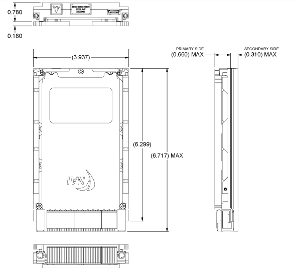
68G6 PART NUMBER DESIGNATION
Click here for the 68G6 part number designation
SYNCHRO/RESOLVER AND LVDT/RVDT SIMULATION MODULE CODE TABLES
Select the Digital-to-Synchro (DSx), Digital-to-Resolver (DRx) or Digital-to-LVDT/RVDT (DLx) module ID corresponding to the application operating parameters required from the following code table (where x = the specific module ID designator). Customer should indicate the actual frequency applicable the design to assure that the correct default band width is set at the factory. All Input and Reference voltages are auto ranging. Frequency/voltage band tolerances +/- 10%. For availability and ranges other than those listed contact the factory. Specifications may be subject to change.
- Single Channel module pending availability (contact factory)
Module ID Format Channel(s) Output Voltage VL-L (Vrms) Reference Voltage (Vrms) Frequency Range (Hz) Power / CH maximum (VA) Notes DS1 SYN 1* 2 - 28 2 - 115 47 - 1 K 3 DR1 RSL DL1 LVDT/RVDT DS2 SYN 1* 2 - 28 2 - 115 1 K - 5 K 3 DR2 RSL DL2 LVDT/RVDT DS3 SYN 1* 2 - 28 2 - 115 5 K - 10 K 3 DR3 RSL DL3 LVDT/RVDT DS4 SYN 1* 2 - 28 2 - 115 10 K - 20 K 3 DR4 RSL DL4 LVDT/RVDT DS5 SYN 1* 28 - 90 2 - 115 47 - 1 K 3 DR5 RSL DL5 LVDT/RVDT DSX SYN 1* X X X X X = TBD; special configuration, requires special part number code designation, contact factory DRX RSL DLX LVDT/RVDT DSA SYN 2 2 - 28 2 - 115 47 - 1 K 1.5 DRA RSL DLA LVDT/RVDT DSB SYN 2 2 - 28 2 - 115 1 K - 5 K 1.5 DRB RSL DLB LVDT/RVDT DSC SYN 2 2 - 28 2 - 115 5 K - 10 K 1.5 DRC RSL DLC LVDT/RVDT DSD SYN 2 2 - 28 2 - 115 10 K - 20 K 1.5 DRD RSL DLD LVDT/RVDT DSE SYN 2 28 - 90 2 - 115 47 - 1 K 2.2 DRE RSL DLE LVDT/RVDT DSY SYN 2 Y Y Y Y Y = TBD; special configuration, requires special part number code designation, contact factory DRY RSL DLY LVDT/RVDT DSJ SYN 3 2 - 28 2 - 115 47 - 1 K 0.5 DRJ RSL DLJ LVDT/RVDT DSK SYN 3 2 - 28 2 - 115 1 K - 5 K 0.5 DRK RSL DLK LVDT/RVDT DSL SYN 3 2 - 28 2 - 115 5 K - 10 K 0.5 DRL RSL DLL LVDT/RVDT DSM SYN 3 2 - 28 2 - 115 10 K - 20 K 0.5 DRM RSL DLM LVDT/RVDT DSN SYN 3 28 - 90 2 - 115 47 - 1 K 0.5 DRN RSL DLN LVDT/RVDT DSZ SYN 3 Z Z Z Z Z = TBD; special configuration, requires special part number code designation, contact factory DRZ RSL DLZ LVDT/RVDT SYNCHRO/RESOLVER AND LVDT/RVDT MEASUREMENT MODULE CODE TABLES
SYN/RSL Four-Channel Measurement (Field Programmable SYN/RSL)
Select the Synchro/Resolver-to-Digital (SDx) module ID corresponding to the application operating parameters required from the following code table (where x = the specific module ID designator). Customer should indicate the actual frequency applicable to the design to assure that the correct default band width is set at the factory. All Input and Reference voltages are auto ranging. For availability and ranges other than those listed contact the factory. Specifications may be subject to change.
Frequency/voltage band tolerances +/- 10%.
Module ID Input Voltage V (Vrms) Reference Voltage + (Vrms) Frequency Range + (Hz) Notes SD1 2 - 28 2 - 115 47 - 1 K SD2 2 - 28 2 - 115 1K - 5 K SD3 2 - 28 2 - 115 5K - 10 K SD4* 2 - 28 2 - 115 10K - 20 K SD5 28 - 90 2 - 115 47 - 1 K SDX* X X X X = TBD; special configuration, requires special part number code designation, contact factory *Consult factory for availability
LVDT/RVDT Four-Channel Measurement (Field Programmable 2, 3 or 4-Wire)
Select the LVDT/RVDT-to-Digital (LDx) module ID corresponding to the application operating parameters required from the following code table (where x = the specific module ID designator). Customer should indicate the actual frequency applicable to the design to assure that the correct default band width is set at the factory. All Input and Excitation voltages are auto ranging. For availability and ranges other than those listed contact the factory. Specifications may be subject to change.
Frequency/voltage band tolerances +/- 10%.
Module ID Input Signal Voltage V + (Vrms) Excitation Voltage + (Vrms) Frequency Range + (Hz) Notes LD1 2 - 28 2 - 115 47 - 1 K LD2 2 - 28 2 - 115 1K - 5 K LD3 2 - 28 2 - 115 5K - 10 K LD4* 2 - 28 2 - 115 10K - 20 K LD5 28 - 90 2 - 115 47 - 1 K LDX* X X X X = TBD; special configuration, requires special part number code designation, contact factory *Consult factory for availability
Link to original
APPENDIX: SUPPORTED IPMI/VITA COMMANDS
The table below shows the complete list of the IPMI and VITA commands supported by the IPMC function, and provides the following details:
- Command Name
- Corresponding IPMI (or VITA) Specification Section
- NetFn (network function) class of the command message
- Corresponding NetFn command offset
- Description of the command
| Command Name | IPMI/VITA Specification Section | NetFn | CMD | Description |
|---|---|---|---|---|
| Set Event Receiver | [IPMI]1.5:23.1 | Sensor/Event (0x04) | 0x00 | Event Command |
| Get Event Receiver | [IPMI]1.5:23.2 | Sensor/Event (0x04) | 0x01 | Event Command |
| Platform Event (aka ‘Event Message’) | [IPMI]1.5:23.3 | Sensor/Event (0x04) | 0x02 | Event Command |
| Get Device SDR Info | [IPMI]1.5:29.2 | Sensor/Event (0x04) | 0x20 | Sensor Device Command |
| Get Device SDR | [IPMI]1.5:29.3 | Sensor/Event (0x04) | 0x21 | Sensor Device Command |
| Reserve Device SDR Repository | [IPMI]1.5:29.4 | Sensor/Event (0x04) | 0x22 | Sensor Device Command |
| Set Sensor Hysteresis | [IPMI]1.5:29.6 | Sensor/Event (0x04) | 0x24 | Sensor Device Command |
| Get Sensor Hysteresis | [IPMI]1.5:29.7 | Sensor/Event (0x04) | 0x25 | Sensor Device Command |
| Set Sensor Threshold | [IPMI]1.5:29.8 | Sensor/Event (0x04) | 0x26 | Sensor Device Command |
| Get Sensor Threshold | [IPMI]1.5:29.9 | Sensor/Event (0x04) | 0x27 | Sensor Device Command |
| Set Sensor Event Enable | [IPMI]1.5:29.10 | Sensor/Event (0x04) | 0x28 | Sensor Device Command |
| Get Sensor Event Enable | [IPMI]1.5:29.11 | Sensor/Event (0x04) | 0x29 | Sensor Device Command |
| Get Sensor Reading | [IPMI]1.5:29.14 | Sensor/Event (0x04) | 0x2D | Sensor Device Command |
| Set Sensor Reading | [IPMI]2.0:35.17 | Sensor/Event (0x04) | 0x30 | Sensor Device Command |
| Get FRU Inventory Area Info | [IPMI]1.5:28.1 | Storage (0x0A) | 0x10 | FRU Device Command |
| Read FRU Data | [IPMI]1.5:28.2 | Storage (0x0A) | 0x11 | FRU Device Command |
| Write FRU Data | [IPMI]1.5:28.3 | Storage (0x0A) | 0x12 | FRU Device Command |
| Get SDR Repository Info | [IPMI]1.5:27.9 | Storage (0x0A) | 0x20 | SDR Device Command |
| Reserve SDR Repository | [IPMI]1.5:27.11 | Storage (0x0A) | 0x22 | SDR Device Command |
| Get SDR | [IPMI]1.5:27.12 | Storage (0x0A) | 0x23 | SDR Device Command |
| Partial Add SDR | [IPMI]1.5:27.14 | Storage (0x0A) | 0x25 | SDR Device Command |
| Clear SDR Repository | [IPMI]1.5:27.16 | Storage (0x0A) | 0x27 | SDR Device Command |
| Get SDR Repository Time | [IPMI]1.5:27.17 | Storage (0x0A) | 0x28 | SDR Device Command |
| Set SDR Repository Time | [IPMI]1.5:27.18 | Storage (0x0A) | 0x29 | SDR Device Command |
| Enter SDR Repository Update Mode | [IPMI]1.5:27.19 | Storage (0x0A) | 0x2A | SDR Device Command |
| Exit SDR Repository Update Mode | [IPMI]1.5:27.20 | Storage (0x0A) | 0x2B | SDR Device Command |
| Get SEL Info | [IPMI]1.5:25.2 | Storage (0x0A) | 0x40 | SEL Device Command |
| Reserve SEL | [IPMI]1.5:25.4 | Storage (0x0A) | 0x42 | SEL Device Command |
| Get SEL Entry | [IPMI]1.5:25.5 | Storage (0x0A) | 0x43 | SEL Device Command |
| Add SEL Entry | [IPMI]1.5:25.6 | Storage (0x0A) | 0x44 | SEL Device Command |
| Clear SEL | [IPMI]1.5:25.9 | Storage (0x0A) | 0x47 | SEL Device Command |
| Get SEL Time | [IPMI]1.5:25.10 | Storage (0x0A) | 0x48 | SEL Device Command |
| Set SEL Time | [IPMI]1.5:25.11 | Storage (0x0A) | 0x49 | SEL Device Command |
| Broadcast ‘Get Device ID’ | [IPMI]1.5:17.9 | Application (0x06) | 0x01 | IPM Device ‘Global’ Command |
| Get Device ID | [IPMI]1.5:17.1 | Application (0x06) | 0x01 | IPM Device ‘Global’ Command |
| Cold Reset | [IPMI]1.5:17.2 | Application (0x06) | 0x02 | IPM Device ‘Global’ Command |
| Warm Reset | [IPMI]1.5:17.3 | Application (0x06) | 0x03 | IPM Device ‘Global’ Command |
| Get Self Test Result | [IPMI]1.5:17.4 | Application (0x06) | 0x04 | IPM Device ‘Global’ Command |
| Get NetFn Support | [IPMI]2.0:21.2 | Application (0x06) | 0x09 | Firmware Firewall Command |
| Get Command Support | [IPMI]2.0:21.3 | Application (0x06) | 0x0A | Firmware Firewall Command |
| Get Command Sub-Function Support | [IPMI]2.0:21.4 | Application (0x06) | 0x0B | Firmware Firewall Command |
| Get Configurable Commands | [IPMI]2.0:21.5 | Application (0x06) | 0x0C | Firmware Firewall Command |
| Get Configurable Commands Sub-Functions | [IPMI]2.0:21.6 | Application (0x06) | 0x0D | Firmware Firewall Command |
| Set BMC Global Enables | [IPMI]1.5:18.1 | Application (0x06) | 0x2E | BMC Device and Messaging Command |
| Get BMC Global Enables | [IPMI]1.5:18.2 | Application (0x06) | 0x2F | BMC Device and Messaging Command |
| Clear Message Flags | [IPMI]1.5:18.3 | Application (0x06) | 0x30 | BMC Device and Messaging Command |
| Get Message Flags | [IPMI]1.5:18.4 | Application (0x06) | 0x31 | BMC Device and Messaging Command |
| Get Message | [IPMI]1.5:18.6 | Application (0x06) | 0x33 | BMC Device and Messaging Command |
| Send Message | [IPMI]1.5:18.7 | Application (0x06) | 0x34 | BMC Device and Messaging Command |
| Master Write-Read | [IPMI]1.5:18.10 | Application (0x06) | 0x52 | BMC Device and Messaging Command |
| Set Command Enables | [IPMI]2.0:21.7 | Application (0x06) | 0x60 | Firmware Firewall Command |
| Get Command Enables | [IPMI]2.0:21.8 | Application (0x06) | 0x61 | Firmware Firewall Command |
| Set Configurable Command Sub-Function Enables | [IPMI]2.0:21.9 | Application (0x06) | 0x62 | Firmware Firewall Command |
| Get Configurable Command Sub-Function Enables | [IPMI]2.0:21.10 | Application (0x06) | 0x63 | Firmware Firewall Command |
| Get OEM NetFn IANA Support | [IPMI]2.0:21.11 | Application (0x06) | 0x64 | Firmware Firewall Command |
| Get VSO Capabilities | [VITA]10.1.3.1 | Group Extension (0x2C) | 0x00 | VITA command, Group ID: VSO (0x03) |
| Set FRU Control | [VITA]10.1.3.6 | Group Extension (0x2C) | 0x04 | VITA command, Group ID: VSO (0x03) |
| Set IPMB State | [VITA]10.1.3.7 | Group Extension (0x2C) | 0x09 | VITA command, Group ID: VSO (0x03) |
| Set FRU State Policy Bits | [VITA]10.1.3.9 | Group Extension (0x2C) | 0x0A | VITA command, Group ID: VSO (0x03) |
| Get FRU State Policy Bits | [VITA]10.1.3.8 | Group Extension (0x2C) | 0x0B | VITA command, Group ID: VSO (0x03) |
| Set FRU Activation | [VITA]10.1.3.10 | Group Extension (0x2C) | 0x0C | VITA command, Group ID: VSO (0x03) |
| Get Device Locator Record ID | [VITA]10.1.3.11 | Group Extension (0x2C) | 0x0D | VITA command, Group ID: VSO (0x03) |
| FRU Control Capabilities | [VITA]10.1.3.18 | Group Extension (0x2C) | 0x1E | VITA command, Group ID: VSO (0x03) |
| Get FRU Address Info | [VITA]10.1.3.3 | Group Extension (0x2C) | 0x40 | VITA command, Group ID: VSO (0x03) |
| Get Mandatory Sensor Numbers | [VITA]10.1.3.26 | Group Extension (0x2C) | 0x44 | VITA command, Group ID: VSO (0x03) |
| Get FRU Hash | [VITA]10.1.3.31 | Group Extension (0x2C) | 0x45 | VITA command, Group ID: VSO (0x03) |
| Get Payload Mode Capabilities | [VITA]10.1.3.32 | Group Extension (0x2C) | 0x46 | VITA command, Group ID: VSO (0x03) |
| Get Control Bits Capabilities | [VITA]10.1.3.40 | Group Extension (0x2C) | 0x4E | VITA command, Group ID: VSO (0x03) |
| Get Control Bits | [VITA]10.1.3.41 | Group Extension (0x2C) | 0x4F | VITA command, Group ID: VSO (0x03) |
| Set Control Bits | [VITA]10.1.3.42 | Group Extension (0x2C) | 0x50 | VITA command, Group ID: VSO (0x03) |
| Get Bridged NetFn Support | [VITA]10.1.3.47 | Group Extension (0x2C) | 0x51 | VITA command, Group ID: VSO (0x03) |
| Get Bridged Command Enables | [VITA]10.1.3.43 | Group Extension (0x2C) | 0x52 | VITA command, Group ID: VSO (0x03) |
| Set Bridged Command Enables | [VITA]10.1.3.44 | Group Extension (0x2C) | 0x53 | VITA command, Group ID: VSO (0x03) |
| Get Bridged Command Sub-Function Enables | [VITA]10.1.3.45 | Group Extension (0x2C) | 0x54 | VITA command, Group ID: VSO (0x03) |
| Set Bridged Command Sub-Function Enables | [VITA]10.1.3.46 | Group Extension (0x2C) | 0x55 | VITA command, Group ID: VSO (0x03) |
| Set Bridged NetFn Policy | [VITA]10.1.3.47 | Group Extension (0x2C) | 0x56 | VITA command, Group ID: VSO (0x03) |
REVISION HISTORY
| Motherboard Manual - TR1 Revision History | ||
| Revision | Revision Date | Description |
| C | 2023-10-12 | ECO C10517, initial release of 68G6 manual. |
| C1 | 2024-03-25 | ECO C11355, pg.6, updated block diagram to remove 'KX' Ethernet references. Pg.6, corrected max commercial temperature. Pg.7, added DLx/DSx(DRx)/SDx to Available Modules table. Pg.15- 17, corrected TTL offsets (changed leading '4' to '8'). Pg.52, corrected Port C color code in color code table. Pg.53, updated Port D color code designation to change '10/100/1000Base-KX' to '10GBase-KR'. Pg.53, updated 2nd table note to change CH1 'KX' port to '1GBase-X'. Pg.58, updated Ethernet Option code 'M' to note that code pertains only to 68G6P w/CH1 configuration. Pg.58, updated Ethernet Option code 'M' to correct CH1 Ethernet signal and clarify routing w/regards to MB Port D. Pg.59, updated Note 4 to add sub-note '2' clarifying CH1 Ethernet signal routing. |
| C2 | 2024-04-11 | ECO C11404, pg.11, removed `/-12V_Aux power from table. Pg.50, removed `/-12V_Aux power from power spec. Pg.51, updated P0 table to remove +/-12V_Aux cell color coding. |
| C3 | 2024-07-03 | ECO C11669, pg.6, updated power spec (from <20W to <11W). Pg.11, updated weight (from <1.6A to <1A). Pg.11, updated power spec (from <20W to <11W). Pg.28, removed US Core/Aux Voltage register descriptions from ‘Motherboard Monitoring Registers’. Pg.28, added verbiage to 'Temperature Readings Register' to clarify use case for register. Pg.28, removed references to Host/Slave processors. Pg.29, updated Temperature Readings table to correct bit descriptions and remove references to Host/Slave processors. Pg.31, Motherboard Health Monitoring Registers section moved to after 'Motherboard Monitoring Registers'. Pg.31, added verbiage to 'Motherboard Health Monitoring Registers' to clarify use case for registers. Pg.31, updated MB Sensor Summary Status register Bit table to change power supply temperature/voltage/current bits to 'reserved'. Pg.31, updated MB Sensor Registers description to better describe register functionality and to add figure. Pg.32, added 'Exceeded' to threshold bit descriptions. Pg.32-33, removed voltage/current references from sensor descriptions. Pg.41, removed US Core/Aux Voltage register offsets. Pg.41, changed Temperature Readings host & slave offsets of Reserved. Pg.41, updated MB Health Monitoring Registers offset tables. Pg.61, Added Appendix: Supported IPMI/VITA Commands. |
DOCS.NAII REVISIONS
| Revision Date | Description |
|---|---|
| 2025-01-30 | Update to address 10G bandwidth limitation - added notation to ‘2x 10GBase-KR Ethernet’ features bullet; added note to ‘Peripheral I/O - Ethernet’ section to describe bandwidth limitation on 10GBase-KR ports. |
| 2025-07-30 | Updated maximum processor speed from 1.3 GHz to 1.2 GHz. |
| 2025-12-03 | Corrected P0 pinout table wafer 5 thru 8 color coding; reformatted default P2 pinout table wafers 9 & 15 to clarify rows G9 & G15 shared pin function/remove duplicated pin designations; reformatted high-speed config P2 pinout table wafers 9 & 15 to clarify rows G9 & G15 shared pin function/remove duplicated pin designations; reformatted optional CH1 module config P2 pinout table wafer 15 to clarify row G15 shared pin function/remove duplicated pin designations. |
NAI Cares
North Atlantic Industries (NAI) is a leading independent supplier of Embedded I/O Boards, Single Board Computers, Rugged Power Supplies, Embedded Systems and Motion Simulation and Measurement Instruments for the Military, Aerospace and Industrial Industries. We accelerate our clients’ time-to-mission with a unique approach based on a Configurable Open Systems Architecture™ (COSA®) that delivers the best of both worlds: custom solutions from standard COTS components.
We have built a reputation by listening to our customers, understanding their needs, and designing, testing and delivering board and system-level products for their most demanding air, land and sea requirements. If you have any applications or questions regarding the use of our products, please contact us for an expedient solution.
Please visit us at: www.naii.com or select one of the following for immediate assistance:
Documentation
FAQ
Application Notes
http://www.naii.com/applicationnotes
Calibration and Repairs
http://www.naii.com/calibrationrepairs
Call Us
(631) 567-1100
Link to original