67G6 DATA SHEET
Click here for the 67G6 data sheet.
INTRODUCtION
NAI is a leading manufacturer of rugged embedded boards, including the 6U OpenVPX Multifunction I/O Board. These boards are designed to meet complex and time-critical sense and response requirements for I/O-intensive, mission-critical applications when paired with NAI’s smart function modules. The 6U OpenVPX Multifunction I/O Board provides a wide range of input and output capabilities, including analog and digital I/O, signal generation and acquisition, and communication interfaces. With features such as conduction cooling and ruggedization, this board is specifically designed to meet the rigorous standards of military and aerospace applications. Its modular I/O approach also makes it a highly flexible and integrable solution for demanding computing environments.
67G6 Overview
The 67G6 6U OpenVPX Multifunction I/O Board offers a variety of features designed to meet the needs of complex and time-critical sense and response requirements for I/O-intensive, mission-critical applications. Some of the key features include:
6U Profiles supported: This board is compatible with both VPX and OpenVPX standards, with module and slot profiles specified as MOD6PER-4U-12.3.3-2 and SLT6-PER-4U-10.3.3, respectively. This allows for interoperability with a wide range of systems.
Connections via front panel, rear panel, or both: The board provides flexibility in connectivity options, with the ability to connect to devices via the front panel, rear panel, or both. This is particularly useful in different mounting or space-constrained scenarios.
Control via Gig-E or PCIe interface: The 67G6 can be controlled via Gig-E or PCIe interface, which provides easy integration into a system.
PCIe connectivity: The board features two PCIe (x1) connectivity options: end point only and direct to module. End point only is used for peripherals, allowing for efficient data transfer between the peripheral and host device, while direct to module is used for high-bandwidth devices, such as graphics cards or solid-state drives, to enable faster data transfer without the need for additional hardware for communication management.
2x 10/100/1000 Base-T or 1000Base-KX Ethernet: The board has two 10/100/1000 Base-T or 1000Base-Kx Ethernet ports, with the option to have one to the rear, one to the front I/O, or both to the rear. These ports provide enhanced data communication capabilities and faster network connectivity for advanced control and data acquisition applications.
IPMC support (option): The 67G6 board has an optional IPMC (Intelligent Platform Management Controller) support, which is VITA 46.11 Tier-2 compatible. This allows for advanced system monitoring and control capabilities to ensure optimal performance and reliability.
Support for six independent, smart function modules: The board can support up to six independent, smart function modules based on the COSA® architecture. With over 100 modules to choose from, this allows for a wide range of input and output capabilities, including analog and digital I/O, signal generation and acquisition, and communication interfaces. Each function module slot also has an independent x1 SerDes interface.
24 channels programmable Discrete I/O (option): The 67G6 has an optional feature of 24 channels programmable Discrete I/O. This option allows users to program I/O channels to perform specific functions based on their needs. The programmable channels support a range of voltages from 0 to 60 VDC and can be configured as Sink, Source or Push/Pull. The board also offers two different function modes Standard (SF) or Enhanced (EF) - to suit different requirements. Overall, this feature offers a highly customizable solution for I/O-intensive applications.
RS232 console/maintenance port: The board features an RS-232 console/maintenance port that provides a standard interface for communicating with the board for maintenance and debugging purposes. This serial port can be used for configuring the board or accessing diagnostic information and logs.
ARM® Cortex®-A53 processor (option): The 67G6 board offers an optional ARM® Cortex®-A53 processor for local I/O processing. The processor is supported by a 2 GB DDR4 + ECC memory module, providing faster data transfer rates and higher bandwidth. Additionally, the board features a standard 32 GB SATA storage technology that enables high-speed data transfer rates and efficient use of space. The board is compatible with PetaLinux, Deos™, and VxWorks® 7 operating systems, offering users a range of options.
Intelligent I/O library support included: The 67G6 comes with intelligent I/O library support to help manage and control the I/O capabilities of the board.
Background Built-In-Test (BIT): The board’s BIT continually checks and reports on the health of each channel, allowing for proactive maintenance and reducing the likelihood of downtime.
Software Support Kits (SSKs) and drivers available: SSKs and drivers are available to make the board easier to integrate into a system and develop software.
VICTORY Interface Services: NAI offers VICTORY Interface Services as an option, providing an open, industry-standard approach for integrating different components in a system.
Commercial and rugged models: The 67G6 is available in both commercial and rugged models, making it suitable for a wide range of applications.
Operating temperature: The board has a wide operating temperature range, with a commercial model operating from 0° C to 70° C, and a rugged model operating from -40° C to +85° C. This makes it suitable for use in a wide range of environments.
Overall, the 67G6 6U OpenVPX Multifunction I/O Board is a reliable and versatile solution for demanding computing environments that require high-performance and flexible I/O capabilities.
SOFTWARE SUPPORT
The ENAIBL Software Support Kit (SSK) is supplied with all system platform based board level products. This platform’s SSK contents include html format help documentation which defines board specific library functions and their respective parameter requirements. A board specific library and its source code is provided (module level ‘C’ and header files) to facilitate function implementation independent of user operating system (O/S). Portability files are provided to identify Board Support Package (BSP) dependent functions and help port code to other common system BSPs. With the use of the provided help documentation, these libraries are easily ported to any 32-bit O/S such as RTOS or Linux.
The latest version of a board specific SSK can be downloaded from our website www.naii.com in the software downloads section. A Quick-Start Software Manual is also available for download where the SSK contents are detailed, Quick-Start Instructions provided and GUI applications are described therein. For other operating system support, contact factory.
Link to original
SPECIFICATIONS
General for the Motherboard
| Signal Logic Level: | Supports LVDS PCIe ver. 2.0 bus (x1) |
| Power (Motherboard): | `5 VDC @ 2.2 A (max) ±12 V @ 0 mA (certain modules may require `/-12 V for operation) +3.3V_AUX @ <100 mA (typical) Then add power for each individual module. |
| Temperature, Operating: | "C" =0° C to +70° C, "H" =-40° C to +85° C (see part number) |
| Storage Temperature: | -55° C to +105° C |
| Temperature Cycling: | Each board is cycled from -40° C to +85° C for option “H” |
| General size: | |
| Height: | 9.2" / 233.7 mm (6U) |
| Width: | 0.8" / 20.32 mm (4HP) or 1.0” / 25.4 mm (5 HP) air cooled front panel options |
| Depth: | 6.3“ / 160 mm deep |
| Weight: | 16 oz. (454 g) unpopulated (approx.) (convection or conduction cooled) >> then add weight for each module (typically 1.5 oz. (42 g) each) |
Specifications are subject to change without notice.
Environmental
Unless otherwise specified, the following table outlines the general Environmental Specifications design guidelines for board level products of North Atlantic Industries. All our cPCI, VME and OpenVPX boards are designed for either air or conduction cooling. All boards also incorporate appropriate stiffening to ensure performance during shock and vibration but also to assure reliable operation (lower fatigue stresses) over the service life of the product.
| Parameters | Level | ||
| 1 / Commercial-AC (Air Cooled) | 2 / Rugged-AC (Air Cooled) | 3 / Rugged-CC (Conduction Cooled) | |
| Temperature - Operating | 0° C to 55° C, AmbientH | -40° C to 85° C, AmbientI | -40° C to 85° C, at wedge lock thermal interface |
| Temperature - Storage | -40° C to 85° C | -55° C to 105° C | -55° C to 105° C |
| Humidity - Operating | 0 to 95%, non-condensing | 0 to 95%, non-condensing | 0 to 95%, non-condensing |
| Humidity - Storage | 0 to 95%, non-condensing | 0 to 95%, non-condensing | 0 to 95%, non-condensing |
| Vibration - SineA | 2 g peak, 15 Hz - 2 kHz^B | 6 g peak, 15 Hz - 2 kHzB | 10 g peak, 15 Hz - 2 kHzC |
| Vibration - RandomD | .002 g2 /Hz, 15 Hz - 2 kHz | 0.04 g2 /Hz, 15 Hz - 2 kHz | 0.1 g2 /Hz, 15 Hz - 2 kHzE |
| ShockF | 20 g peak, half-sine, 11 ms | 30 g peak, half-sine 11 ms | 40 g peak, half-sine, 11 ms |
| Low PressureG | Up to 15,000 ft. | Up to 50,000 ft. | Up to 50,000 ft. |
Notes:
A. Based on sweep duration of ten minutes per axis on each of the three mutually perpendicular axes. B. Displacement limited to 0.10 D.A. from 15 to 44 Hz. C. Displacement limited to 0.436 D.A. from 15 to 21 Hz. D. 60 minutes per axis on each of the three mutually perpendicular axes. E. Per MIL-STD-810G, Method 5.14.6 Procedure I, Fig.514.6C-6 Category 7 tailored (11.65 Grms): 15 Hz - 2 kHz; ASD (PSD) at 0.04 g2/Hz between 15 Hz - 150 Hz, increasing @ 4 dB/octave from 0.04 g2/Hz to 0.1 g /Hz between 150 Hz - 300 Hz, 0.1 g2/Hz between 300 Hz - 1000 Hz, decreasing @ 6 dB/octave from 0.1 g2/Hz to 0.025 g2/Hz between 1000 Hz - 2000 Hz. Three hits per direction per axis (total of 18 hits). F. Three hits per direction per axis (total of 18 hits). G. For altitudes higher than 50,000 ft., contact NAI. H. High temperature operation requires 350 lfm minimum air flow across cover/heatsink (module dependent). I. High temperature operation requires 600 lfm minimum air flow across cover/heatsink (module dependent).
Specifications subject to change without notice
REGISTER MEMORY MAP ADDRESSING
The register map address consists of the following:
• cPCI/PCIe BAR or Base Address for the Board • Module Slot Base Address • Function Offset Address
Board Base Address
The table below lists the BAR used for access to the motherboard and module registers. The second BAR is used internally for motherboard and module firmware updates. The other cPCI/PCIe BARs not listed are not used.
| NAI Boards | Device ID | Bus | Motherboard and Module Register Access | Motherboard and Module Firmware Updates |
| Slave Boards | ||||
| 67G6 | 0x6781 | PCIe | BAR 1 Size: Module Dependent (minimum 64K Bytes) | BAR 2 Size: 1M Bytes |
Module Slot and Function Addresses
The memory map for the modules are dependent on the types of modules on the board and the order in which the modules are installed on the board as well as the firmware installed on the motherboard. The function modules are enumerated allowing for dynamic memory space allocation and therefore the “start” address of the module function register area is factory pre-defined (and read from) the Module Address register. Refer to Figure 1 for an example.
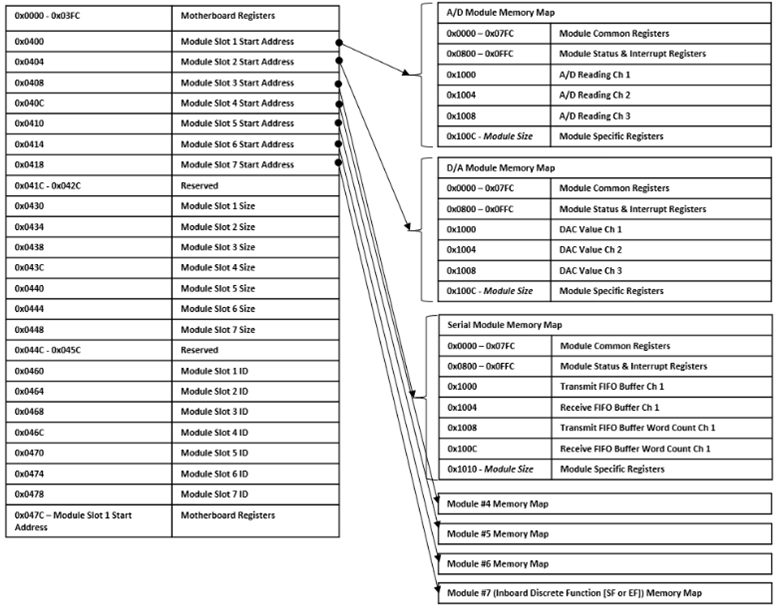
Figure 1. Register Memory Map Addressing for Motherboards with 7 Modules
Address Calculation
Motherboard Registers
Read/Write access to the motherboard registers starts with the base address for the board and then the motherboard base offset address.
For example, to address Module Slot 1 Start Address register (i.e. register address = 0x0400):
- Start with the base address for the board.
- Add the motherboard base register address offset.
| Motherboard Address = | Base Address Motherboard Address Offset | = 0x9000 0400 |
| 0x9000 0000 + 0x0400 |
Module Registers:
Read/Write access to the Function module’s registers start with the base address of the board. Add the “content” for the Module Start Address and then, add the specific module function register offset.
For example, to address an appropriate/specific function module with a register offset:
- Start with the base address for the board.
- Add the value (contents) from the module base address offset register (contents/value of Motherboard Memory register for Module 1 (i.e., @ 0x0400) = 0x4000.
- Then add the specific module function Register Offset of interest (i.e., A/D Reading Ch 1 @ 0x1000)
| (Function Specific) Address = | Base Address + | Module Base Address Offset + | Function Register Offset | = 0x9000 5000 |
| 0x9000 0000 | 0x4000 | 0x1000 |
REGISTER DESCRIPTIONS
The register descriptions provide the Register Name, Type, Data Range, Read or Write information, power on default initialized values, a description of the function and a data table where applicable.
Module Information Registers
The Module Slot Addressing Ready register indicates that the module slots are ready to be addressed. Module Slot Address, Module Slot Size and Module Slot ID provide information about the modules detected on the board.
Module Slot Addressing Ready
Link to original
Function: Indicates that the module slots are ready to be addressed. Type: unsigned binary word (32-bit) Data Range: 0x0000 0000 to 0xFFFF FFFF Read/Write: R Initialized Value: 0xA5A5A5A5 Operational Settings: This register will contain the value of 0xA5A5A5A5 when the module addresses have been determined.
Link to original
Module Slot Address Function: Specifies the Base Address for the module in the specific slot position. Type: unsigned binary word (32-bit) Data Range: 0x0000 0000 to 0xFFFF FFFF Read/Write: R Initialized Value: Based on board's module configuration. Operational Settings: 0x0000 0000 indicates no Module found.
Link to original
Module Slot Size Function: Specifies the Memory Size (in bytes) allocated for the module in the specific slot position. Type: unsigned binary word (32-bit) Range: 0x0000 0000 to 0xFFFF FFFF Read/Write: R Initialized Value: Assigned by factory for the module. Operational Settings: 0x0000 0000 indicates no Module found.
Module Slot ID Function: Specifies the Model ID for the module in the specified slot position. Type: 4-character ASCII string Data Range: 0x0000 0000 to 0xFFFF FFFF Read/Write: R Initialized Value: Assigned by factory for the module. Operational Settings: The Module ID is formatted as four ASCII bytes: three characters followed by a space. Module IDs are in little-endian order with a single space following the first three characters. For example, 'TL1' is '1LT', 'SC1' is '1CS' and so forth. Example below is for “TL1” (MSB justified). All value of 0000 0000 indicates no Module found. Link to original
D31 D30 D29 D28 D27 D26 D25 D24 D23 D22 D21 D20 D19 D18 D17 D16 ASCII Character (ex: 'T' - 0x54) ASCII Character (ex: 'L' - 0x4C) D15 D14 D13 D12 D11 D10 D9 D8 D7 D6 D5 D4 D3 D2 D1 D0 ASCII Character (ex: '1' - 0x31) ASCII Space (' ' - 0x20)
Hardware Information Registers
The registers identified in this section provide information about the board’s hardware.
Link to original
Product Serial Number Function: Specifies the Board Serial Number. Type: unsigned binary word (32-bit) Data Range: 0x0000 0000 to 0xFFFF FFFF Read/Write: R Initialized Value: Serial number assigned by factory for the board. Operational Settings: N/A
Platform
Function: Specifies the Board Platform Identifier. Values are for the ASCII characters for the NAI valid platforms (Identifiers).
Type: unsigned binary word (32-bit)
Data Range: See table below.
Read/Write: R
Initialized Value: ASCII code is for the Platform Identifier of the board
Operational Settings: Valid NAI platform and the associated value for the platform is shown below:
| NAI Platform | Platform Identifier | ASCII Binary Values (Note: little-endian order of ascii values) |
|---|---|---|
| 3U VPX | 67 | 0x0000 3837 |
Model
Function: Specifies the Board Model Identifier. Value is for the ASCII characters for the NAI valid model.
Type: unsigned binary word (32-bit)
Data Range: See table below.
Read/Write: R
Initialized Value: ASCII code is for the Model Identifier of the board
Operational Settings: Example of NAI model and the associated value for the model is shown below:
| NAI Model | ASCII Binary Values (Note: little-endian order of ascii values) |
|---|---|
| G | 0x0000 0047 |
Generation
Function: Specifies the Board Generation. Identifier values are for the ASCII characters for the NAI valid generation identifiers.
Type: unsigned binary word (32-bit)
Data Range: See table below.
Read/Write: R
Initialized Value: ASCII code is for the Generation Identifier of the board
Operational Settings: Example of NAI generation and the associated value for the generation is shown below:
| NAI Generation | ASCII Binary Values (Note: little-endian order of ascii values) |
|---|---|
| 6 | 0x0000 0036 |
Processor Count/Ethernet Count
Function: Specifies the Processor Count and Ethernet Count
Type: unsigned binary word (32-bit)
Data Range: See table below.
Read/Write: R
Operational Settings:
Processor Count - Integer: indicates the number of unique processor types on the motherboard.
| NAI Board | Processor Count | Description | |
| 6U-VPX | 67G6 | 1 | Xilinx Zynq UltraScale+ |
Ethernet Interface Count - Indicates the number of Ethernet interfaces on the product motherboard. For example, Single Ethernet = 1; Dual
Ethernet = 2.
Processor/Ethernet Interface Count
| D31 | D30 | D29 | D28 | D27 | D26 | D25 | D24 | D23 | D22 | D21 | D20 | D19 | D18 | D17 | D16 |
| Processor Count (See Table) | |||||||||||||||
| D15 | D14 | D13 | D12 | D11 | D10 | D9 | D8 | D7 | D6 | D5 | D4 | D3 | D2 | D1 | D0 |
| Ethernet Count (Based on Part Number Ethernet Options) | |||||||||||||||
Maximum Module Slot Count/ARM Platform Type
Function: Specifies the Maximum Module Slot Count and ARM Platform Type.
Type: unsigned binary word (32-bit)
Data Range: See table below.
Read/Write: R
Operational Settings:
Maximum Module Slot Count - 7
ARM Platform - Xilinx UltraScale = 3
Maximum Module Slot Count / ARM Platform Type
| D31 | D30 | D29 | D28 | D27 | D26 | D25 | D24 | D23 | D22 | D21 | D20 | D19 | D18 | D17 | D16 |
| Maximum Module Slot Count = 0x0007 | |||||||||||||||
| D15 | D14 | D13 | D12 | D11 | D10 | D9 | D8 | D7 | D6 | D5 | D4 | D3 | D2 | D1 | D0 |
| ARM Platform Type = 0x0003 (UltraScale) | |||||||||||||||
Processor Operating System Registers
The registers in this section provide information about the Operating System that is running on the host processor on the motherboard. For boards that have more than one processor (ex. 75PPC1, 75INT2, 68PPC2, etc), the host processor would be the Power-PC or Intel processor.
ARM Processor Platform
Function: Specifies the ARM Processor on the motherboard. Values are for the ASCII characters for the NAI host processor platforms specified by the Operating System. Type: 8-character ASCII string - Two (2) unsigned binary word (32-bit) Data Range: N/A Read/Write: R Initialized Value: ASCII code is for the Host Platform Identifier of the board. Operational Settings: Valid NAI platforms based on Operating System loaded to host processor. Link to original
Processor Platform (Note: 8-character ASCII string) (“aarch64”) Word 1 (0x6372 6161 = “craa”) D31 D30 D29 D28 D27 D26 D25 D24 D23 D22 D21 D20 D19 D18 D17 D16 'c' (0x63) 'r' (0x72) D15 D14 D13 D12 D11 D10 D9 D8 D7 D6 D5 D4 D3 D2 D1 D0 'a' (0x61) 'a' (0x61) Word 2 (0x0034 3668 = “ 46h”) D31 D30 D29 D28 D27 D26 D25 D24 D23 D22 D21 D20 D19 D18 D17 D16 null (0x00) '4' (0x34) D15 D14 D13 D12 D11 D10 D9 D8 D7 D6 D5 D4 D3 D2 D1 D0 '6' (0x36) 'h' (0x68)
Processor Operating System
Function: Specifies the Operating System installed for the host processor. Values are for the ASCII characters for the NAI supported operating systems. Type: 12-character ASCII string - Three (3) unsigned binary word (32-bit) Data Range: N/A Read/Write: R Operational Settings: ASCII, 12 characters; ('Linux', 'VxWorks', 'RTOS', ...) Link to original
Processor Platform (Note: 12-character ASCII string) (“Linux”) Word 1 (0x756E 694C = “uniL”) D31 D30 D29 D28 D27 D26 D25 D24 D23 D22 D21 D20 D19 D18 D17 D16 'u' (0x75) 'n' (0x6E) D15 D14 D13 D12 D11 D10 D9 D8 D7 D6 D5 D4 D3 D2 D1 D0 'i' (0x69) 'L' (0x4C) Word 2 (0x0000 0078 = “ x”) D31 D30 D29 D28 D27 D26 D25 D24 D23 D22 D21 D20 D19 D18 D17 D16 null (0x00) null (0x00) D15 D14 D13 D12 D11 D10 D9 D8 D7 D6 D5 D4 D3 D2 D1 D0 null (0x00) null (0x00) Word 3 (0x0000 0000 = “ ”) D31 D30 D29 D28 D27 D26 D25 D24 D23 D22 D21 D20 D19 D18 D17 D16 null (0x00) null (0x00) D15 D14 D13 D12 D11 D10 D9 D8 D7 D6 D5 D4 D3 D2 D1 D0 null (0x00) null (0x00)
Processor Operating System Version
Function: Specifies the Version of Operating System installed for the host processor. Type: 8-character ASCII string - Two (2) unsigned binary word (32-bit) Data Range: N/A Read/Write: R Operational Settings: ASCII, 8 characters Link to original
Processor OS Version (Note: little-endian order of ascii values) (ex. “4.14.0”) Word 1 (Ex. 0x3431 2E34 = “41.4”) D31 D30 D29 D28 D27 D26 D25 D24 D23 D22 D21 D20 D19 D18 D17 D16 ex: '4' (0x34) ex: '1' (0x31) D15 D14 D13 D12 D11 D10 D9 D8 D7 D6 D5 D4 D3 D2 D1 D0 ex: '.' (0x2E) ex: '3' (0x33) Word 2 (Ex.0x 0000 302E = “ 0.”) D31 D30 D29 D28 D27 D26 D25 D24 D23 D22 D21 D20 D19 D18 D17 D16 null (0x00) null (0x00) D15 D14 D13 D12 D11 D10 D9 D8 D7 D6 D5 D4 D3 D2 D1 D0 ex: '0' (0x30) ex: '.' (0x2E)
Motherboard Firmware Information Registers
The registers in this section provide information on the revision of the firmware installed on the motherboard.
Transclude of Mb-Fpga-Firmware-Version-67Ppc2
Motherboard Firmware Build Time/Date
Function: Specifies the Build Date/Time of the NAI factory provided Motherboard Core Application installed on the board. Type: Two (2) unsigned binary word (32-bit) Data Range: N/A Read/Write: R Operational Settings: The motherboard firmware time consists of the Build Date and Build Time.
NOTE: On some builds the the Date/Time fields are fixed to 0000 0000 to maintain binary consistency across builds.Link to original
Motherboard Firmware Build Time (Note: little-endian order in register) Word 1 - Build Date (ex. 0x0E05 07E5 = 2021-5-14) D31 D30 D29 D28 D27 D26 D25 D24 D23 D22 D21 D20 D19 D18 D17 D16 Day (ex: 0x0E = 14) Month (ex: 0x05 = 5) D15 D14 D13 D12 D11 D10 D9 D8 D7 D6 D5 D4 D3 D2 D1 D0 Year (ex: 0x07E5 = 2021) Word 2 - Build Time (ex. 0x0005 3712 = 18:55:05) D31 D30 D29 D28 D27 D26 D25 D24 D23 D22 D21 D20 D19 D18 D17 D16 null (0x00) Seconds (ex: 0x05 = 05) D15 D14 D13 D12 D11 D10 D9 D8 D7 D6 D5 D4 D3 D2 D1 D0 Minutes (ex: 0x37 = 55) Hours (ex: 0x12 = 18)
Motherboard FPGA Compile Date/Time
Function: Specifies the Compile Date/Time of the NAI factory provided Motherboard FPGA installed on the board. Type: unsigned binary word (32-bit) Data Range: N/A Read/Write: R Operational Settings: The motherboard firmware time consists of the Build Date and Time in the following format: .
Link to original
Motherboard FPGA Compile Time (ex. 0xD22B 1809 = 04/26/21 17:32:09) D31 D30 D29 D28 D27 D26 D25 D24 D23 D22 D21 D20 D19 D18 D17 D16 Day (D31:D27) Month (D26:D23) Year (D22:D17) ex. 0xD ex. 0x2 0x2 0xB Day = 0x1A = 26 Month = 0x4 = 4 Year = 0x15 = 21 D15 D14 D13 D12 D11 D10 D9 D8 D7 D6 D5 D4 D3 D2 D1 D0 Hour (D16:D12) Minutes (D11:D6) Seconds (D5:D0) ex. 0x1 ex. 0x8 ex. 0x0 ex. 0x9 0 0 0 1 1 0 0 0 0 0 0 0 1 0 0 1 Hour = 0x11 = 17 Minutes = 0x20 = 32 Seconds = 0x09 = 09
Motherboard Monitoring Registers
The registers in this provide motherboard temperature measurement information.
Temperature Readings Register
The temperature registers provide the current, maximum (from power-up) and minimum (from power-up) for the processor and PCB for UltraScale processor.
These registers are only available on Xilinx Generation 5 platforms, and are periodically populated by the motherboard core application, which only runs in Petalinux and BareMetal. For other operating systems, refer to the naibrd Software Support Kit (SSK) naibsp_system_Monitor_Temperature_Get() routine to manually retrieve the temperature (NOTE: this feature is typically utilized for development/factory use only; contact the factory for additional details on potential use, if required).
Function: Specifies the Measured Temperatures on Motherboard. Type: signed byte (8-bits) for each temperature reading - Six (6) 32-bit words Data Range: 0x0000 0000 to 0xFFFF 0000 Read/Write: R Initialized Value: Value corresponding to the measured temperatures based on the table below. Operational Settings: The 8-bit temperature readings are signed bytes. For example, if the following register contains the value 0x2B2B 0000: Example:
Word 1 (UltraScale Temperatures) D31 D30 D29 D28 D27 D26 D25 D24 D23 D22 D21 D20 D19 D18 D17 D16 UltraScale Core Temperature UltraScale PCB Temperature D15 D14 D13 D12 D11 D10 D9 D8 D7 D6 D5 D4 D3 D2 D1 D0 0x00 0x00 The values would represent the following temperatures:
Temperature Measurements Data Bits Value Temperature (Celsius) UltraScale Core Temperature D31:D24 0x2B +43° UltraScale PCB Temperature D23:D16 0x2B +43° Link to original
Temperature Readings Word 1 (UltraScale Temperatures) D31 D30 D29 D28 D27 D26 D25 D24 D23 D22 D21 D20 D19 D18 D17 D16 UltraScale Core Temperature UltraScale PCB Temperature D15 D14 D13 D12 D11 D10 D9 D8 D7 D6 D5 D4 D3 D2 D1 D0 0x00 0x00 Word 2 (Reserved) D31 D30 D29 D28 D27 D26 D25 D24 D23 D22 D21 D20 D19 D18 D17 D16 0x00 0x00 D15 D14 D13 D12 D11 D10 D9 D8 D7 D6 D5 D4 D3 D2 D1 D0 0x00 0x00 Word 3 (Max UltraScale Temperatures) D31 D30 D29 D28 D27 D26 D25 D24 D23 D22 D21 D20 D19 D18 D17 D16 Max UltraScale Core Temperature Max UltraScale PCB Temperature D15 D14 D13 D12 D11 D10 D9 D8 D7 D6 D5 D4 D3 D2 D1 D0 0x00 0x00 Word 4 (Reserved) D31 D30 D29 D28 D27 D26 D25 D24 D23 D22 D21 D20 D19 D18 D17 D16 0x00 0x00 D15 D14 D13 D12 D11 D10 D9 D8 D7 D6 D5 D4 D3 D2 D1 D0 0 0 0 0 0 0 0 0 0 0 0 0 0 0 0 0 Word 5 (Min UltraScale Temperatures) D31 D30 D29 D28 D27 D26 D25 D24 D23 D22 D21 D20 D19 D18 D17 D16 Min UltraScale Core Temperature Min UltraScale PCB Temperature D15 D14 D13 D12 D11 D10 D9 D8 D7 D6 D5 D4 D3 D2 D1 D0 0 0 0 0 0 0 0 0 0 0 0 0 0 0 0 0 Word 6 (Reserved) D31 D30 D29 D28 D27 D26 D25 D24 D23 D22 D21 D20 D19 D18 D17 D16 0x00 0x00 D15 D14 D13 D12 D11 D10 D9 D8 D7 D6 D5 D4 D3 D2 D1 D0 0 0 0 0 0 0 0 0 0 0 0 0 0 0 0 00
Higher Precision Temperature Readings Registers
These registers provide higher precision readings of the current UltraScale Core and PCB temperatures.
Higher Precision UltraScale Core Temperature
Function: Specifies the Higher Precision Measured UltraScale Core temperature on Motherboard Board. Type: signed word (16-bits) for integer part and unsigned word (16-bits) for fractional part Data Range: 0x0000 0000 to 0xFFFF FFFF Read/Write: R Initialized Value: Measured UltraScale Core temperature on Motherboard Board Operational Settings: The upper 16-bits represent the signed integer part of the temperature, and the lower 16-bits represent the fractional part of the temperature with the resolution of 1/1000 of degree Celsius. For example, if the register contains the value 0x002B 0271, this represents UltraScale Core Temperature = 43.625° Celsius, and value 0xFFF6 0177 represents -10.375° Celsius. Link to original
D31 D30 D29 D28 D27 D26 D25 D24 D23 D22 D21 D20 D19 D18 D17 D16 Signed Integer Part of Temperature D15 D14 D13 D12 D11 D10 D9 D8 D7 D6 D5 D4 D3 D2 D1 D0 Fractional Part of Temperature
Higher Precision Motherboard PCB Temperature Function: Specifies the Higher Precision Measured Motherboard PCB temperature. Type: signed word (16-bits) for integer part and unsigned word (16-bits) for fractional part Data Range: 0x0000 0000 to 0xFFFF FFFF Read/Write: R Initialized Value: Measured Motherboard PCB temperature Operational Settings: The upper 16-bits represent the signed integer part of the temperature and the lower 16-bits represent the fractional part of the temperature with the resolution of 1/1000 of degree Celsius. For example, if the register contains the value 0x0020 007D, this represents Interface PCB Temperature = 32.125° Celsius, and value 0xFFE8 036B represents -24.875° Celsius. Link to original
D31 D30 D29 D28 D27 D26 D25 D24 D23 D22 D21 D20 D19 D18 D17 D16 Signed Integer Part of Temperature D15 D14 D13 D12 D11 D10 D9 D8 D7 D6 D5 D4 D3 D2 D1 D0 Fractional Part of Temperature
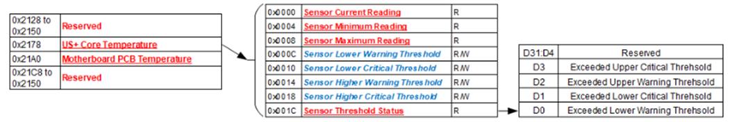
Motherboard Health Monitoring Registers
The registers in this section provide a summary of motherboard temperature sensors and their corresponding bits. Additionally, this section provides an overview of the registers allocated to those sensors, which are used to monitor current/minimum/maximum temperature readings, upper & lower critical/warning temperature thresholds, and whether or not a programmed temperature threshold has been exceeded.
These registers are only available on Xilinx Generation 5 platforms, and are periodically populated by the motherboard core application, which only runs in Petalinux and BareMetal. For other operating systems, refer to the naibrd Software Support Kit (SSK) naibsp_system_Monitor_Temperature_Get() routine to manually retrieve the temperature (NOTE: this feature is typically utilized for development/factory use only; contact the factory for additional details on potential use, if required).
Transclude of Sensor-Summary-Status-Us
Transclude of Mb-Sensor-Registers-Us
Sensor Threshold Status Function: Reflects which threshold has been crossed Type: unsigned binary word (32-bits) Data Range: See table below Read/Write: R Initialized Value: 0 Operational Settings: The associated bit is set when the sensor reading exceed the corresponding threshold settings. Link to original
Bit(s) Description D31:D4 Reserved D3 Exceeded Upper Critical Threshold D2 Exceeded Upper Warning Threshold D1 Exceeded Lower Critical Threshold D0 Exceeded Lower Warning Threshold
Link to original
Sensor Current Reading Function: Reflects current reading of temperature sensor Type: Single Precision Floating Point Value (IEEE-754) Data Range: Single Precision Floating Point Value (IEEE-754) Read/Write: R Initialized Value: N/A Operational Settings: The register represents current sensor reading as a single precision floating point value. For example, for a temperature sensor, register value 0x41C6 0000 represents temperature = 24.75° Celsius.
Link to original
Sensor Minimum Reading Function: Reflects minimum value of temperature sensor since power up Type: Single Precision Floating Point Value (IEEE-754) Data Range: Single Precision Floating Point Value (IEEE-754) Read/Write: R Initialized Value: N/A Operational Settings: The register represents minimum sensor value as a single precision floating point value. For example, for a temperature sensor, register value 0x41C6 0000 represents temperature = 24.75° Celsius.
Link to original
Sensor Maximum Reading Function: Reflects maximum value of temperature sensor since power up Type: Single Precision Floating Point Value (IEEE-754) Data Range: Single Precision Floating Point Value (IEEE-754) Read/Write: R Initialized Value: N/A Operational Settings: The register represents maximum sensor value as a single precision floating point value. For example, for a temperature sensor, register value 0x41C6 0000 represents temperature = 24.75° Celsius.
Link to original
Sensor Lower Warning Threshold Function: Reflects lower warning threshold of temperature sensor Type: Single Precision Floating Point Value (IEEE-754) Data Range: Single Precision Floating Point Value (IEEE-754) Read/Write: R/W Initialized Value: Default lower warning threshold (value dependent on specific sensor) Operational Settings: The register represents sensor lower warning threshold as a single precision floating point value. For example, for a temperature sensor, register value 0xC220 0000 represents temperature = -40.0° Celsius.
Link to original
Sensor Lower Critical Threshold Function: Reflects lower critical threshold of temperature sensor Type: Single Precision Floating Point Value (IEEE-754) Data Range: Single Precision Floating Point Value (IEEE-754) Read/Write: R/W Initialized Value: Default lower critical threshold (value dependent on specific sensor) Operational Settings: The register represents sensor lower critical threshold as a single precision floating point value. For example, for a temperature sensor, register value 0xC25C 0000 represents temperature = -55.0° Celsius.
Link to original
Sensor Upper Warning Threshold Function: Reflects upper warning threshold of temperature sensor Type: Single Precision Floating Point Value (IEEE-754) Data Range: Single Precision Floating Point Value (IEEE-754) Read/Write: R/W Initialized Value: Default upper warning threshold (value dependent on specific sensor) Operational Settings: The register represents sensor upper warning threshold as a single precision floating point value. For example, for a temperature sensor, register value 0x42AA 0000 represents temperature = 85.0° Celsius.
Link to original
Sensor Upper Critical Threshold Function: Reflects upper critical threshold of temperature sensor Type: Single Precision Floating Point Value (IEEE-754) Data Range: Single Precision Floating Point Value (IEEE-754) Read/Write: R/W Initialized Value: Default upper critical threshold (value dependent on specific sensor) Operational Settings: The register represents sensor upper critical threshold as a single precision floating point value. For example, for a temperature sensor, register value 0x42FA 0000 represents temperature = 125.0° Celsius.
Ethernet Configuration Registers
The registers in this section provide information about the Ethernet Configuration for the two ports on the board.
Important: Regardless if the board is configured for one or two Ethernet ports, the second IP address cannot be on the same Subnet as the First IP Address. The table below provides examples of valid and invalid IP Addresses and Subnet Mask Addresses.
Link to original
First Port (A) IP Address First Port (A) Subnet Mask Second Port (B) IP Address Second Port (B) Subnet Mask Result 192.168.1.5 255.255.255.0 192.168.2.5 255.255.255.0 Good 192.168.1.5 255.255.0.0 192.168.2.5 255.255.0.0 Conflict 192.168.1.5 255.255.0.0 192.168.2.5 255.255.255.0 Conflict 10.0.0.15 255.0.0.0 192.168.1.5 255.255.255.0 Good
Ethernet MAC Address and Ethernet Settings Function: Specifies the Ethernet MAC Address and Ethernet Settings for the Ethernet port. Type: Two (2) unsigned binary word (32-bit) Data Range: See table. Read/Write: R Operational Settings: The Ethernet MAC Address consists of six octets. The Ethernet Settings are defined in table.
Bits Description Values D31:D23 Reserved 0 D22:D21 Duplex 00 = Not Specified, ` 01 = Half Duplex, ` 10 = Full Duplex, + 11 = Reserved D20:D18 Speed 000 = Not Specified, ` 001 = 10 Mbps, ` 010 = 100 Mbps, ` 011 = 1000 Mbps, ` 100 = 2500 Mbps, ` 101 = 10000 Mbps, ` 110 = Reserved, + 111 = Reserved D17 Auto Negotiate 0 = Enabled, + 1 = Disabled D16 Static IP Address 0 = Enabled, + 1 = Disabled Link to original
Ethernet MAC Address and Ethernet Settings (Note: little-endian order in register) Word 1 (Ethernet MAC Address (Octets 1-4)) (ex: aa:bb:cc:dd:ee:ff) D31 D30 D29 D28 D27 D26 D25 D24 D23 D22 D21 D20 D19 D18 D17 D16 MAC Address Octet 4 (ex: 0xDD) MAC Address Octet 3 (ex: 0xCC) D15 D14 D13 D12 D11 D10 D9 D8 D7 D6 D5 D4 D3 D2 D1 D0 MAC Address Octet 2 (ex: 0xBB) MAC Address Octet 1 (ex: 0xAA) Word 2 (Ethernet MAC Address (Octets 5-6) and Ethernet Settings) D31 D30 D29 D28 D27 D26 D25 D24 D23 D22 D21 D20 D19 D18 D17 D16 Ethernet Settings (See table) D15 D14 D13 D12 D11 D10 D9 D8 D7 D6 D5 D4 D3 D2 D1 D0 MAC Address Octet 6 (ex: 0xFF) MAC Address Octet 5 (ex: 0xEE)
Ethernet Interface Name Function: Specifies the Ethernet Interface Name for the Ethernet port. Type: 8-character ASCII string Data Range: See table. Read/Write: R Operational Settings: The Ethernet Interface Name (eth0, eth1, etc) for the Ethernet port. Link to original
Ethernet Interface Name (Note: ascii string in register) (ex. “eth0”) Word 1 (Bit 0-31) (ex: 0x3068 7465 = “0hte”) D31 D30 D29 D28 D27 D26 D25 D24 D23 D22 D21 D20 D19 D18 D17 D16 ASCII Character (ex: '0' - 0x30) ASCII Character (ex: 'h' - 0x68) D15 D14 D13 D12 D11 D10 D9 D8 D7 D6 D5 D4 D3 D2 D1 D0 ASCII Character (ex: 't' - 0x74) ASCII Character (ex: 'e' - 0x65) Word 2 (Bit 32-63) (ex: 0x0000 0000) D31 D30 D29 D28 D27 D26 D25 D24 D23 D22 D21 D20 D19 D18 D17 D16 ASCII Character (ex: null - 0x00) ASCII Character (ex: null - 0x00) D15 D14 D13 D12 D11 D10 D9 D8 D7 D6 D5 D4 D3 D2 D1 D0 ASCII Character (ex: null - 0x00) ASCII Character (ex: null - 0x00)
Ethernet IPv4 Address Function: Specifies the Ethernet IPv4 Address for the Ethernet port. Type: Three (3) unsigned binary word (32-bit) Data Range: See table. Read/Write: R Operational Settings: The Ethernet IPv4 Address consists of three parts: IPv4 Address, IPv4 Subnet Mask and IPv4 Gateway. Link to original
Ethernet IPv4 Address (Note: little-endian order in register) Word 1 (Ethernet IPv4 Address) (ex: 0x1001 A8C0 = 192.168.1.16) D31 D30 D29 D28 D27 D26 D25 D24 D23 D22 D21 D20 D19 D18 D17 D16 IPv4 Address Octet 4 (ex: 0x10 = 16) IPv4 Address Octet 3 (ex: 0x01 = 1) D15 D14 D13 D12 D11 D10 D9 D8 D7 D6 D5 D4 D3 D2 D1 D0 IPv4 Address Octet 2 (ex: 0xA8 = 168) IPv4 Address Octet 1 (ex: 0xC0 = 192) Word 2 (Ethernet IPv4 Subnet) (ex: 0x00FF FFFF = 255.255.255.0) D31 D30 D29 D28 D27 D26 D25 D24 D23 D22 D21 D20 D19 D18 D17 D16 IPv4 Subnet Octet 4 (ex: 0x00 = 0) IPv4 Subnet Octet 3 (ex: 0xFF = 255) D15 D14 D13 D12 D11 D10 D9 D8 D7 D6 D5 D4 D3 D2 D1 D0 IPv4 Subnet Octet 2 (ex: 0xFF = 255) IPv4 Subnet Octet 1 (ex: 0xFF = 255) Word 3 (Ethernet IPv4 Gateway) (ex: 0x0101 A8C0 = 192.168.1.1) D31 D30 D29 D28 D27 D26 D25 D24 D23 D22 D21 D20 D19 D18 D17 D16 IPv4 Gateway Octet 4 (ex: 0x01 = 1) IPv4 Gateway Octet 3 (ex: 0x01 = 1) D15 D14 D13 D12 D11 D10 D9 D8 D7 D6 D5 D4 D3 D2 D1 D0 IPv4 Gateway Octet 2 (ex: 0xA8 = 168) IPv4 Gateway Octet 1 (ex: 0xC0 = 192)
Ethernet IPv6 Address Function: Specifies the Ethernet IPv6 Address for the Ethernet port. Type: Five (5) unsigned binary word (32-bit) Data Range: See table. Read/Write: R Operational Settings: The IPv6 Prefix length indicates the network portion of an IPv6 address using the following format: IPv6 address/prefix length ` Prefix length can range from 0 to 128 ` * Typical prefix length is 64 The following is an illustration of IPv6 addressing with IPv6 Prefix length of 64.
64 bits 64 bits Prefix Interface ID Prefix 1 Prefix 2 Prefix 3 Subnet ID Interface ID 1 Interface ID 2 Interface ID 3 Interface ID 4 Example: 2002:c0a8:101:0:7c99:d118:9058:1235/64 2002 C0A8 0101 0000 7C99 D118 9058 1235 Link to original
Ethernet IPv6 Address (Note: little-endian order within 32-bit and 16-bit words in register) (ex. IPv6 Address: 2002:c0a8:201:0:7c99:d118:9058:1235 IPv6 Prefix: 64) Word 1 (Ethernet IPv6 Address (Prefix 1-2)) (ex:0xA8C0 0220 = 2002 C0A8) D31 D30 D29 D28 D27 D26 D25 D24 D23 D22 D21 D20 D19 D18 D17 D16 Prefix 2 (ex: 0xA8C0 = C0A8) D15 D14 D13 D12 D11 D10 D9 D8 D7 D6 D5 D4 D3 D2 D1 D0 Prefix 1 (ex: 0x0220 = 2002) Word 2 (Ethernet IPv6 Address (Prefix 3/Subnet ID)) + (ex:0x000 0101 = 0101 0000) D31 D30 D29 D28 D27 D26 D25 D24 D23 D22 D21 D20 D19 D18 D17 D16 Subnet ID (ex: 0x0000 = 0000) D15 D14 D13 D12 D11 D10 D9 D8 D7 D6 D5 D4 D3 D2 D1 D0 Prefix 3 (ex: 0x0101 = 0101) Word 3 (Ethernet IPv6 Address (Interface ID 1-2)) + (ex: 0x18D1 997C = 7C99 D118) D31 D30 D29 D28 D27 D26 D25 D24 D23 D22 D21 D20 D19 D18 D17 D16 Interface ID 2 (ex: 0x18D1 = D118) D15 D14 D13 D12 D11 D10 D9 D8 D7 D6 D5 D4 D3 D2 D1 D0 Interface ID 1 (ex: 0x997C = 7C99) Word 4 (Ethernet IPv6 Address (Interface ID 3-4)) + (ex: 0x3512 5890 = 9058 1235) D31 D30 D29 D28 D27 D26 D25 D24 D23 D22 D21 D20 D19 D18 D17 D16 Interface ID 4 (ex: 0x3512 = 1235) D15 D14 D13 D12 D11 D10 D9 D8 D7 D6 D5 D4 D3 D2 D1 D0 Interface ID 3 (ex: 0x5890 = 9058) Word 5 (Ethernet IPv6 Prefix Length) + (ex:0x0000 0040) D31 D30 D29 D28 D27 D26 D25 D24 D23 D22 D21 D20 D19 D18 D17 D16 0 0 0 0 0 0 0 0 0 0 0 0 0 0 0 0 D15 D14 D13 D12 D11 D10 D9 D8 D7 D6 D5 D4 D3 D2 D1 D0 Prefix Length (ex: 0x0040 = 64)
Interrupt Vector and Steering
When interrupts are enabled, the interrupt vector associated with the specific interrupt can be programmed (typically with a unique number/identifier) such that it can be utilized in the Interrupt Service Routine (ISR) to identify the type of interrupt. When an interrupt occurs, the contents of the Interrupt Vector registers is reported as part of the interrupt mechanism. In addition to specifying the interrupt vector, the interrupt can be directed (“steered”) to the native bus or to the application running on the onboard ARM processor.
Note
The Interrupt Vector and Interrupt Steering registers are mapped to the Motherboard Common Memory and these registers are associated with the Module Slot position (refer to Function Register Map).
Interrupt Vector Function: Set an identifier for the interrupt. Type: unsigned binary word (32-bit) Data Range: 0x0000 0000 to 0xFFFF FFFF Read/Write: R/W Initialized Value: 0 Operational Settings: When an interrupt occurs, this value is reported as part of the interrupt mechanism.
Interrupt Steering Function: Sets where to direct the interrupt. Type: unsigned binary word (32-bit) Data Range: See table Read/Write: R/W Initialized Value: 0 Operational Settings: When an interrupt occurs, the interrupt is sent as specified: Link to original
Direct Interrupt to VME 1 Direct Interrupt to ARM Processor (via SerDes) +
(Custom App on ARM or NAI Ethernet Listener App)2 Direct Interrupt to PCIe Bus 5 Direct Interrupt to cPCI Bus 6
Modules Health Monitoring Registers
Module BIT Status
Function: Provides the ability to monitor the individual Module BIT Status.
Type: unsigned binary word (32-bit)
Data Range: 0x0000 0000 to 0xFFFF FFFF
Read/Write: R
Operational Settings: The Module BIT Status registers provide the ability to monitor individual Module BIT results as Latched and current value. A 1 is any bit field indicates BIT failure for the Module in that slot.
Module BIT Status
Link to original
Bit(s) Description D31:24 Reserved D23 Module Slot 7 BIT Failure (current value) D22 Module Slot 6 BIT Failure (current value) D21 Module Slot 5 BIT Failure (current value) D20 Module Slot 4 BIT Failure (current value) D19 Module Slot 3 BIT Failure (current value) D18 Module Slot 2 BIT Failure (current value) D17 Module Slot 1 BIT Failure (current value) D16 Reserved D8-15 Reserved D7 Module Slot 7 BIT Failure – Latched D6 Module Slot 6 BIT Failure – Latched D5 Module Slot 5 BIT Failure – Latched D4 Module Slot 4 BIT Failure – Latched D3 Module Slot 3 BIT Failure – Latched D2 Module Slot 2 BIT Failure – Latched D1 Module Slot 1 BIT Failure – Latched D0 Reserved
Scratchpad Area
Link to original
Scratchpad Area Function: Registers reserved as scratch pad for customer use. Type: unsigned binary word (32-bit) Data Range: 0x0000 0000 to 0xFFFF FFFF Read/Write: R/W Operational Settings: This area in memory is reserved for customer use.
MOTHERBOARD FUNCTION REGISTER MAP
Key:
Bold Underline = Measurement/Status/Board Information
Bold Italic = Configuration/Control
Module Information Registers
| 0x03FC | Module Slot Addressing Ready | R |
|---|
| 0x0400 | Module Slot 1 Address | R |
|---|---|---|
| 0x0404 | Module Slot 2 Address | R |
| 0x0408 | Module Slot 3 Address | R |
| 0x040C | Module Slot 4 Address | R |
| 0x0410 | Module Slot 5 Address | R |
| 0x0414 | Module Slot 6 Address | R |
| 0x0418 | Module Slot 7 Address | R |
| 0x0430 | Module Slot 1 Size | R |
|---|---|---|
| 0x0434 | Module Slot 2 Size | R |
| 0x0438 | Module Slot 3 Size | R |
| 0x043C | Module Slot 4 Size | R |
| 0x0440 | Module Slot 5 Size | R |
| 0x0444 | Module Slot 6 Size | R |
| 0x0448 | Module Slot 7 Size | R |
| 0x0460 | Module Slot 1 ID | R |
|---|---|---|
| 0x0464 | Module Slot 2 ID | R |
| 0x0468 | Module Slot 3 ID | R |
| 0x046C | Module Slot 4 ID | R |
| 0x0470 | Module Slot 5 ID | R |
| 0x0474 | Module Slot 6 ID | R |
| 0x0478 | Module Slot 7 ID | R |
Hardware Information Registers
| 0x0020 | Product Serial Number | R |
|---|
| 0x0024 | Platform | R |
|---|---|---|
| 0x0028 | Model | R |
| 0x002C | Generation | R |
| 0x0030 | Processor Count/Ethernet Count | R |
|---|---|---|
| 0x0034 | Maximum Module Slot Count/ARM Platform Type | R |
| 0x0038 | Processor Platform (Bit 0-31) | R |
|---|---|---|
| 0x003C | Processor Platform (Bit 32-63) | R |
| 0x0040 | Processor Operating System (Bit 0-31) | R |
|---|---|---|
| 0x0044 | Processor Operating System (Bit 32-63) | R |
| 0x0048 | Processor Operating System (Bit 64-95) | R |
| 0x004C | Processor Operating System Version (Bit 0-31) | R |
|---|---|---|
| 0x0050 | Processor Operating System Version (Bit 32-63) | R |
Motherboard Firmware Information Registers
Motherboard Core Information
| 0x0100 | MB Core Major/Minor Version | R |
|---|---|---|
| 0x0104 | MB Core Minor 2/3 Version | R |
| 0x0108 | MB Core Build Date (Bit 0-31) | R |
| 0x010C | MB Core Build Date (Bit 32-63) | R |
Motherboard FPGA Information
| 0x0270 | MB FPGA Revision | R |
|---|---|---|
| 0x0274 | MB FPGA Compile Date/Time | R |
Motherboard Monitoring Registers
Temperature Readings
| 0x0200 | Current UltraScale Temperatures | R |
|---|---|---|
| 0x0204 | Reserved | R |
| 0x0208 | Max UltraScale Temperatures | R |
| 0x020C | Reserved | R |
| 0x0210 | Min UltraScale Temperatures | R |
| 0x0214 | Reserved | R |
Higher Precision Temperature Readings
| 0x0230 | Current UltraScale Core Temperature | R |
|---|---|---|
| 0x0234 | Current UltraScale PCB Temperature | R |
Motherboard Health Monitoring Registers
| 0x20F8 | Motherboard Sensor Summary Status | R |
|---|
Ethernet Configuration Registers
| 0x0070 | Ethernet A MAC (Octets 1-4) | R |
|---|---|---|
| 0x0074 | Ethernet A MAC (Octets 5-6)/Misc Settings | R |
| 0x0078 | Ethernet A Interface Name (Bit 0-31) | R |
|---|---|---|
| 0x007C | Ethernet A Interface Name (Bit 32-63) | R |
| 0x0080 | Ethernet A IPv4 Address | R |
|---|---|---|
| 0x0084 | Ethernet A IPv4 Subnet Mask | R |
| 0x0088 | Ethernet A IPv4 Gateway | R |
| 0x008C | Ethernet A IPv6 Address (Prefix 1-2) | R |
|---|---|---|
| 0x0090 | Ethernet A IPv6 Address (Prefix 3/Subnet ID) | R |
| 0x0094 | Ethernet A IPv6 Address (Interface ID 1-2) | R |
| 0x0098 | Ethernet A IPv6 Address (Interface ID 3-4) | R |
| 0x009C | Ethernet A IPv6 Prefix Length | R |
| 0x00A0 | Ethernet B MAC (Octets 1-4) | R |
|---|---|---|
| 0x00A4 | Ethernet B MAC (Octets 5-6)/Misc Settings | R |
| 0x00A8 | Ethernet B Interface Name (Bit 0-31) | R |
|---|---|---|
| 0x00AC | Ethernet B Interface Name (Bit 32-63) | R |
| 0x00B0 | Ethernet B IPv4 Address | R |
|---|---|---|
| 0x00B4 | Ethernet B IPv4 Subnet Mask | R |
| 0x00B8 | Ethernet B IPv4 Gateway | R |
| 0x00BC | Ethernet B IPv6 Address (Prefix 1-2) | R |
|---|---|---|
| 0x00C0 | Ethernet B IPv6 Address (Prefix 3/Subnet ID) | R |
| 0x00C4 | Ethernet B IPv6 Address (Interface ID 1-2) | R |
| 0x00C8 | Ethernet B IPv6 Address (Interface ID 3-4) | R |
| 0x00CC | Ethernet B IPv6 Prefix Length | R |
Interrupt Vector and Steering
| 0x0500 - 0x057C | Module 1 Interrupt Vector 1 - 32 | R/W |
|---|---|---|
| 0x0700 - 0x077C | Module 2 Interrupt Vector 1 - 32 | R/W |
| 0x0900 - 0x097C | Module 3 Interrupt Vector 1 - 32 | R/W |
| 0x0B00 - 0x0B7C | Module 4 Interrupt Vector 1 - 32 | R/W |
| 0x0D00 - 0x0D7C | Module 5 Interrupt Vector 1 - 32 | R/W |
| 0x0F00 - 0x0F7C | Module 6 Interrupt Vector 1 - 32 | R/W |
| 0x1100 - 0x117C | Module 7 Interrupt Vector 1 - 32 | R/W |
| 0x0600 - 0x067C | Module 1 Interrupt Steering 1 - 32 | R/W |
|---|---|---|
| 0x0800 - 0x087C | Module 2 Interrupt Steering 1 - 32 | R/W |
| 0x0A00 - 0x0A7C | Module 3 Interrupt Steering 1 - 32 | R/W |
| 0x0C00 - 0x0C7C | Module 4 Interrupt Steering 1 - 32 | R/W |
| 0x0E00 - 0x0E7C | Module 5 Interrupt Steering 1 - 32 | R/W |
| 0x1000 - 0x107C | Module 6 Interrupt Steering 1 - 32 | R/W |
| 0x1200 - 0x127C | Module 7 Interrupt Steering 1 - 32 | R/W |
Modules Health Monitoring Registers
Module BIT Status
| 0x0128 | Module BIT Status (current and latched) | R |
|---|
Scratchpad Registers
| 0x3800 - 0x3BFF | Scratchpad Registers | R/W |
|---|
ETHERNET
(For detailed supplement, please visit the NAI web-site specific product page and refer to: Ethernet Interface for Generation 5 SBC and Embedded IO Boards Specification)
Note
For products capable of 10/100/1000Base-KX functionality - the product Ethernet PHY supports 1000BASE-X. Product interoperability with 10/100/1000BASE-KX is supported with 1000BASE-X (provided that auto-negotiation is disabled).
The Ethernet Interface Option allows communications and control access to all function modules either via the system BUS or Ethernet ports 1 or 2.
Ethernet 1 Ethernet 2 Ethernet 3* Ethernet 4* (REF PORT A) (REF PORT B) (REF PORT C) (REF PORT D) The default IP address: 192.168.1.16 192.168.2.16 192.168.3.16 192.168.4.16 The default subnet: 255.255.255.0 255.255.255.0 255.255.255.0 255.255.255.0 The default gateway: 192.168.1.1 192.168.2.1 192.168.3.1 192.168.4.1 *see Part Number Designation for applicability.
Note
Actual “as shipped” card Ethernet default IP addresses may vary based upon final ATP configuration(s).
The NAI interface supports IPv4 and IPv6 and both the TCP and UDP protocols. The Ethernet Operation Mode Command Listener application running on the motherboard host processor implements the operation interface. The listener is operational on startup through the nai_MBStartup process and listen on specific ports for commands to process. The default ports are listed below:
- TCP1 - Port 52801
- TCP2 - Port 52802
- UDP1 - Port 52801
- UDP2 - Port 52802
While the listener is active, note that interrupts from the motherboard do not trigger. The listener can be disabled by turning off the nai_MBStartup process through the Motherboard EEPROM. To turn off nai_MBStartup use the command mbeeprom_util set MBStartupInitOnlyFlag 1 in the console, either by serial port or telnet to the motherboard, and then reboot the system. To turn on the nai_MBStartup use the command mbeeprom_util set MBStartupInitOnlyFlag 0 in the console, either by serial port or telnet to the motherboard, and then reboot the system.
Ethernet Message Framework
The interface uses a specific message framework for all commands and responses. All messages begin with a Preamble code and end with a Postamble code. The message framework is shown below.
Preamble
2 bytes Always
0xD30FSequenceNo
2 bytesType Code
2 byteMessage Length
(2 bytes)Payload
(0..1414 bytes)Postamble
2 bytes
Always
0xF03DMessage Elements
Preamble The Preamble is used to delineate the beginning of a message frame.
The Preamble is always 0xD30F.SequenceNo The SequenceNo is used to associate Commands with Responses. Type Code Type Codes are used to define the type of Command or Response the message contains. Message Length The Message Length is the number of bytes in the complete message frame starting with and including the
Preamble and ending with and including the Postamble.Payload The Payload contains the unique data that makes up the command or response.
Payloads vary based on command type.Postamble The Postamble is use to delineate the end of a message frame.
The Postamble is always 0xF03D.Notes
- The messaging protocol applies only to card products.
- Messaging is managed by the connected (client) computer. The client computer will send a single message and wait for a reply from the card. Multiple cards may be managed from a single computer, subject to channel and computer capacity.
Board Addressing
The interface provides two main addressing areas: Onboard and Off-board.
Onboard addressing refers to accessing resources located on the board that is implementing the operation interface (including its modules).
Off-board addressing refers to accessing resources located on another board reachable via VME, PCI, or other bus. Off-board addressing requires a Master/Slave configuration.
The user must always specify if a particular address is Onboard or Off-board. See the command descriptions for the onboard and off-board flags.
Within a particular board (Onboard or Off-board), the address space is broken up into two areas: Motherboard Common Address Space and Module Address Space. All addresses are 32-bit.
Motherboard Common Address Space starts at 0x00000000 and ends at 0x00004000. This is a 4Kx32-bit address space (16 kbytes).
Module Address Space starts at 0x00004000. Module addressing is dynamically configured at startup. NAI boards support between 1 and 6 modules. The minimum module address space size is 4Kx32 (16 kbytes) and module sizes are always a multiple of 4Kx32.
Module addressing is dynamic and cumulative. The first detected module (starting with Slot 1) is given an address of 0x00004000. The 2nd detected Module is given an address of:
First_Detected_Module_Address + First_Detected_Module_Size
Note
Slots do not define addresses.
If no module is detected in a module slot, that slot is not given an address. Therefore, if the first detected Module is in Slot 2, then that module address will be 0x00004000. If the next detected module is in Slot 4, then the address of that Module will be:
Second_Detected_Module_Address = First_Detected_Module_Address + First_Detected_Module_Size
If a 3rd Module is detected in Slot 6, then the address of that Module will be:
Third_Detected_Module_Address = Second_Detected_Module_Address + Second_Detected_Module_Size
Note
Module addresses are calculated at each board startup when the modules are detected. Therefore, if a module should fail to be detected due to malfunction or because it was removed from the motherboard, the addresses of the modules that follow it in the slot sequence will be altered. This is important to note when programming to this interface.
Users can always retrieve the Module Addresses, Module Sizes and Module IDs from the fixed Motherboard Common address area. This data is set upon each board startup. While the Module Addressing is dynamic, the address where these addresses are stored is fixed. For example, to find the startup address of the module location in Slot 3, refer to the MB Common Address 0x00000408 from the Motherboard Common Addresses table that follows.
Ethernet Wiring Convention
Link to original
RJ-45 Pin T568A Color T568B Color 10/100Base-T 1000BASE-T NAI wiring convention 1 white/green stripe white/orange stripe TX+ DA+ ETH-TP0+ 2 green orange TX- DA- ETH-TP0- 3 white/orange stripe white/green stripe RX+ DB+ ETH-TP1+ 4 blue blue DC+ ETH-TP2+ 5 white/blue stripe white/blue stripe DC- ETH-TP2- 6 orange green RX- DB- ETH-TP1- 7 white/brown stripe white/brown stripe DD+ ETH-TP3+ 8 brown brown DD- ETH-TP3-
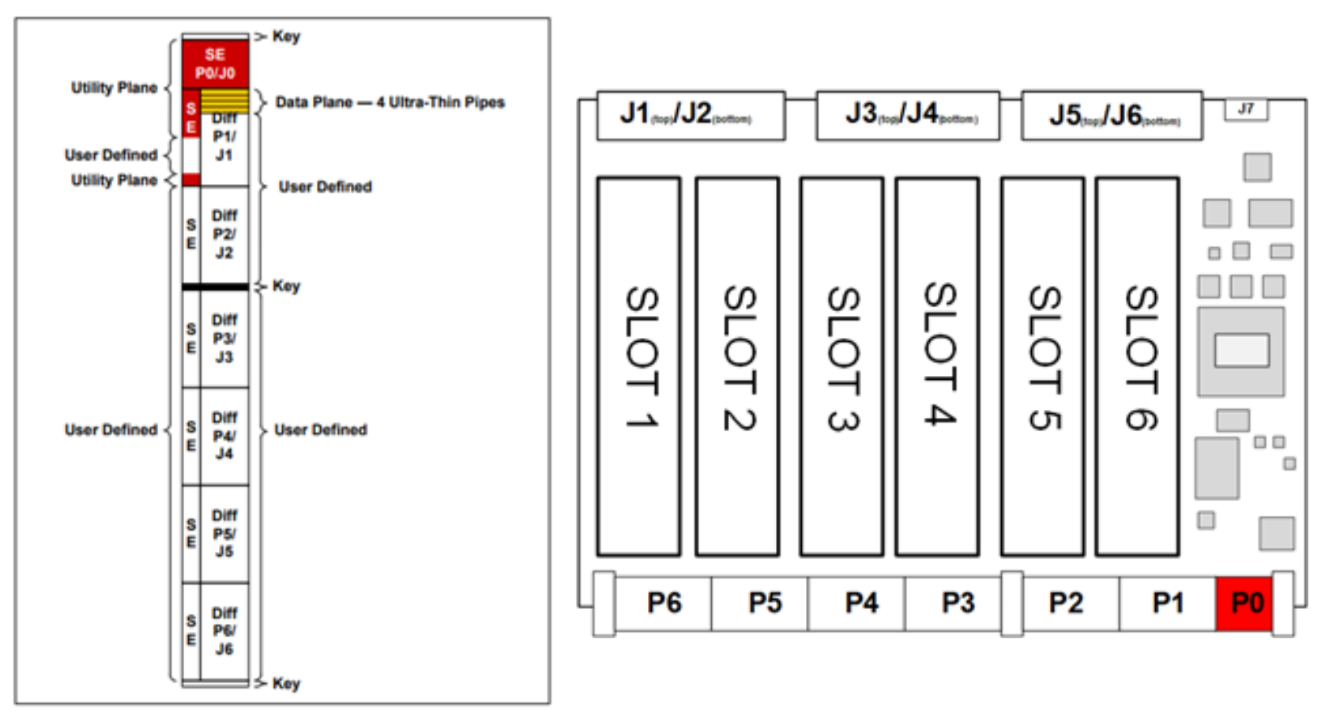
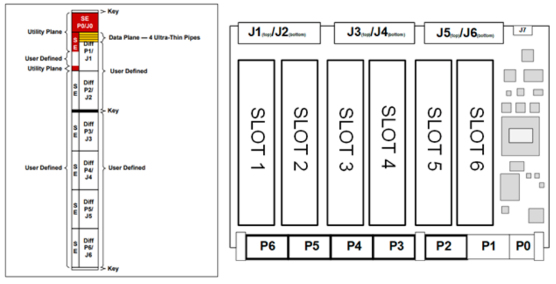
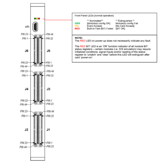
67G6 CONNECTOR/PIN-OUT INFORMATION
Front and Rear Panel Connectors
The 67G6 6U OpenVPX Multifunction I/O board is available in two configurations: convection-cooled and conduction-cooled. The 67G6 follows the OpenVPX “Payload Slot Profile” configured as:
| Slot profile: | SLT6-PER-4U-10.3.3 |
|---|---|
| Module profile: | MOD6-PER-4U-12.3.3-2 |
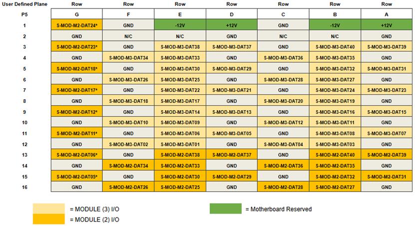
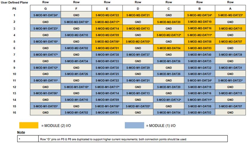
User I/O is available through the (J1, J2, J3, J4, J5, J6) front panel connectors when the card is configured with front panel I/O and through the OpenVPX user defined rear I/O connectors P3, P4, P5, P6 (see part number and pin-out information).
Notes
The following notes apply unless otherwise specified:
Front Panel Connectors J1 - J6 (Convection-Cooled)
44-pin male connectors, 2mm, Harwin P/N M80-5114422.
Mate kit: “Custom Hood Kit” part # M80C108448C (or equivalent); Includes connector, backshell, pins & jackscrews. This mating connector kit may be purchased separately as NAI P/N 05-0119 (contact factory).
Panel LEDs
Front Panel LEDs indications (only available on air-cooled units).
| LED | ILLUMINATED | EXTINGUISHED |
|---|---|---|
| GRN: | Blinking: Initializing Steady On: Power-On/Ready | Power off |
| RED: | Module BIT error | No BIT fault |
| YEL: (flash) | Card access (bus or Gig-E activity) | No card activity |
Chassis Ground
Front Panel Connectors: J1 - J6 pin-1 is chassis GND. Jack screw sockets are chassis GND.
Rear Connectors: Not available.
Front Panel System (Power/Signal) Ground Reference
Front Panel: J1 - J6 pin-23 is System (SYS) GND (referenced to card power/system ground).
Front I/O Utility Connector J7 (Convection and Conduction-Cooled)*
The 67G6 utilizes a Mini-HDMI type card edge connector J7, available on either convection or conduction-cooled configurations that provides the following signals:
-
Serial (port 1)
-
Ethernet port 1 (factory configuration option - Ethernet port1 may be redirected to rear I/O J2)
NAI also provides an optional “breakout” adapter board (NAI P/N 75SBC4-BB) with a mini-HDMI to mini-HDMI type cable. The “breakout” adapter board and a Micro-HDMI cable (NAI P/N 75SBC4-BB) allow for standard I/O connections to Ethernet and asynchronous serial (DB9). Consult the factory for availability.
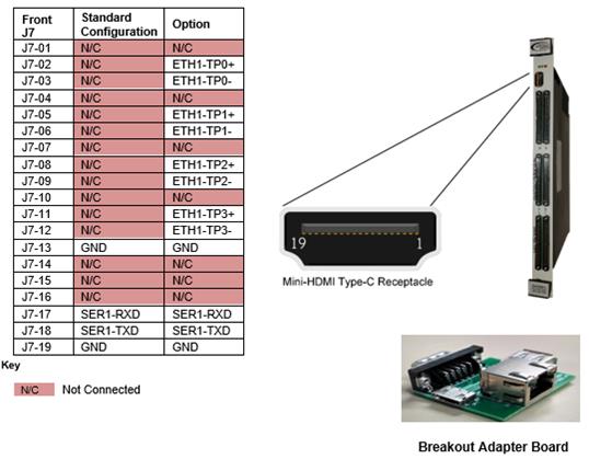
Signal Descriptions J7
| Signal Name | Description |
|---|---|
| ETH1-TPx | Ethernet port 1 signals (4 pair) 10/100/1000 twisted pair signals (Optional - available only if NOT re-directed to rear I/O (see part number configuration options) |
| SER1-TXD | Asynchronous transmit serial data port 1 (out) / RS232 debug/console port only |
| SER1-RXD | Asynchronous received serial data port 1 (in) / RS232 debug/console port only |
| GND | System Ground (return) |
Rear I/O VPX Connectors P0-P6 (Conduction-Cooled)
The 67G6 6U OpenVPX multifunction I/O board provides interface via the rear VPX connectors.
Rear I/O Summary
Signals defined as N/C currently have no functionality associated and are not required for general operation.
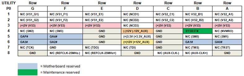
P0 - Utility plane. Contains the following signal definitions:
| Power: Primary: | +5V, 3.3V, /- 12V and System GND |
|---|---|
| Geographical Address Pins: | GA0# - GA4#, GAP# |
| Card reset: | SYSRST# signal |
| Non-Volatile Memory Read Only: | NVMRO |
| IPMC: | IMPB-SDA-A, IMPB-SDA-B, IMPB-SCL-A, IMPB-SCL-B |
| VPX AUX/REF CLK: | (Not used) |
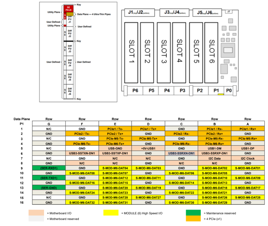
P1 - Defined as Data/Control Planes (User defined I/O secondary)
| High Speed Switched Fabric Interface: | 2 x1 PCIe (end point only) 2 x1 PCIe (direct to module) |
|---|---|
| Ethernet: | Dual Gig-E port option(s) are available and defined (See Part Number Designation section) |
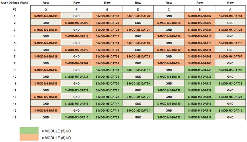
P2 - Defined as Expansion Plane (User defined I/O secondary)
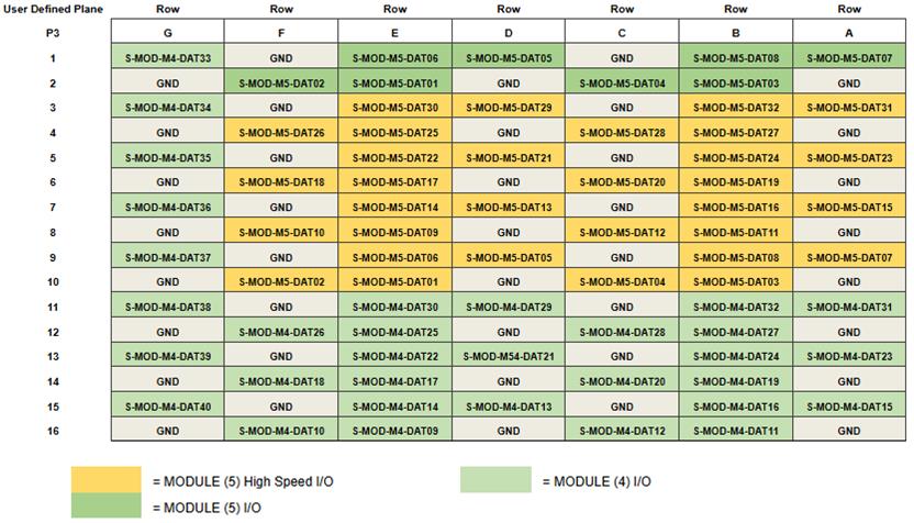
P3 - User defined I/O (primary)
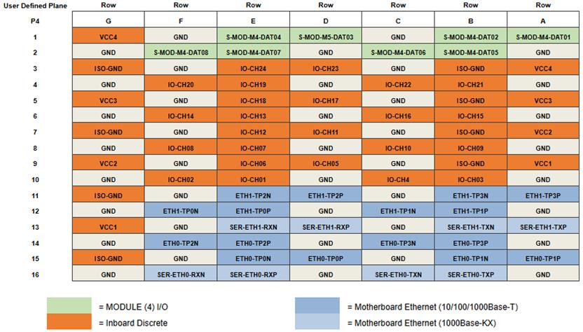
P4 - User defined I/O (primary)
P5 - User defined I/O (primary)
P6 - User defined I/O (primary)
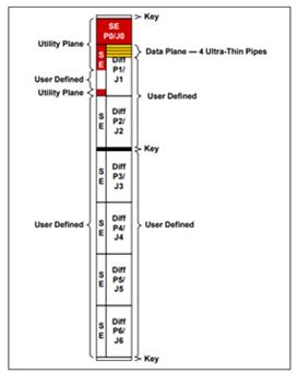
Rear I/O Utility Plane (P0)
The P0 (Utility) Plane contains the primary power, bus and utility signals for the OpenVPX board. Additionally, several of the user defined pins can be utilized for Geographical Addressing and a parallel SYSRST# signal. Signals defined as N/C currently have no functionality associated and is not required for general operation.
Rear I/O Data/Control Planes (P1)
The 67G6 has a four PCIe ver 2.0 Ultra-Thin pipes. Two provide communication to the motherboard (end point) and two provide direct communication to two function module locations (direct to module, for Function Module 5 and 6). Additionally, the 67G6 can be commanded/controlled via dual port Gig-E (options for either 10/100/1000Base-T and/or 1000Base-KX (SerDes) Interfaces). Additional module I/O is also defined on the P1 user defined plane. Signals defined as N/C currently have no functionality associated or are considered optional and are not required for general operation.
USER I/O - Defined Area (User Defined I/O) (P2-P6)
The following pages contain the ‘user defined’ I/O data area front and rear panel pin-outs with their respective signal designations for all module types currently offered/configured for the 67G6 platform. The card is designed to route the function module I/O signals to the front and rear I/O connector. The following I/O connector pin-out is based upon the function module designated in the module slot. Signals defined as N/C currently have no functionality associated or are considered optional and are not required for general operation.
J1-J6 Front Panel Connector Pinout Mapping Summary (Convection-Cooled)
The following provides connector/pinout data for Front Panel connectors J1 through J6. Each connector provides 44 pins of I/O.
.67G6 J1 (M1) Front Panel I/O
| (System Ground REF) | GND | 1 | 23 | GND | (System Ground REF) |
|---|---|---|---|---|---|
| M1_DAT01 | S-MOD-M1-DAT01 | 2 | 24 | S-MOD-M1-DAT02 | M1_DAT02 |
| M1_DAT03 | S-MOD-M1-DAT03 | 3 | 25 | S-MOD-M1-DAT04 | M1_DAT04 |
| M1_DAT25 | S-MOD-M1-DAT25 | 4 | 26 | S-MOD-M1-DAT26 | M1_DAT26 |
| M1_DAT05 | S-MOD-M1-DAT05 | 5 | 27 | S-MOD-M1-DAT06 | M1_DAT06 |
| M1_DAT33 | S-MOD-M1-DAT33 | 6 | 28 | S-MOD-M1-DAT34 | M1_DAT34 |
| M1_DAT07 | S-MOD-M1-DAT07 | 7 | 29 | S-MOD-M1-DAT08 | M1_DAT08 |
| M1_DAT09 | S-MOD-M1-DAT09 | 8 | 30 | S-MOD-M1-DAT10 | M1_DAT10 |
| M1_DAT27 | S-MOD-M1-DAT27 | 9 | 31 | S-MOD-M1-DAT28 | M1_DAT28 |
| M1_DAT11 | S-MOD-M1-DAT11 | 10 | 32 | S-MOD-M1-DAT12 | M1_DAT12 |
| M1_DAT35 | S-MOD-M1-DAT35 | 11 | 33 | S-MOD-M1-DAT36 | M1_DAT36 |
| M1_DAT13 | S-MOD-M1-DAT13 | 12 | 34 | S-MOD-M1-DAT14 | M1_DAT14 |
| M1_DAT15 | S-MOD-M1-DAT15 | 13 | 35 | S-MOD-M1-DAT16 | M1_DAT16 |
| M1_DAT29 | S-MOD-M1-DAT29 | 14 | 36 | S-MOD-M1-DAT30 | M1_DAT30 |
| M1_DAT17 | S-MOD-M1-DAT17 | 15 | 37 | S-MOD-M1-DAT18 | M1_DAT18 |
| M1_DAT37 | S-MOD-M1-DAT37 | 16 | 38 | S-MOD-M1-DAT38 | M1_DAT38 |
| M1_DAT19 | S-MOD-M1-DAT19 | 17 | 39 | S-MOD-M1-DAT20 | M1_DAT20 |
| M1_DAT21 | S-MOD-M1-DAT21 | 18 | 40 | S-MOD-M1-DAT22 | M1_DAT22 |
| M1_DAT31 | S-MOD-M1-DAT31 | 19 | 41 | S-MOD-M1-DAT32 | M1_DAT32 |
| M1_DAT23 | S-MOD-M1-DAT23 | 20 | 42 | S-MOD-M1-DAT24 | M1_DAT24 |
| M1_DAT39 | S-MOD-M1-DAT39 | 21 | 43 | S-MOD-M1-DAT40 | M1_DAT40 |
| N/C | 22 | 44 | N/C |
.67G6 J2 (M2) Front Panel I/O
| (System Ground REF) | GND | 1 | 23 | GND | (System Ground REF) |
|---|---|---|---|---|---|
| M2_DAT01 | S-MOD-M2-DAT01 | 2 | 24 | S-MOD-M2-DAT02 | M2_DAT02 |
| M2_DAT03 | S-MOD-M2-DAT03 | 3 | 25 | S-MOD-M2-DAT04 | M2_DAT04 |
| M2_DAT25 | S-MOD-M2-DAT25 | 4 | 26 | S-MOD-M2-DAT26 | M2_DAT26 |
| M2_DAT05 | S-MOD-M2-DAT05 | 5 | 27 | S-MOD-M2-DAT06 | M2_DAT06 |
| M2_DAT33 | S-MOD-M2-DAT33 | 6 | 28 | S-MOD-M2-DAT34 | M2_DAT34 |
| M2_DAT07 | S-MOD-M2-DAT07 | 7 | 29 | S-MOD-M2-DAT08 | M2_DAT08 |
| M2_DAT09 | S-MOD-M2-DAT09 | 8 | 30 | S-MOD-M2-DAT10 | M2_DAT10 |
| M2_DAT27 | S-MOD-M2-DAT27 | 9 | 31 | S-MOD-M2-DAT28 | M2_DAT28 |
| M2_DAT11 | S-MOD-M2-DAT11 | 10 | 32 | S-MOD-M2-DAT12 | M2_DAT12 |
| M2_DAT35 | S-MOD-M2-DAT35 | 11 | 33 | S-MOD-M2-DAT36 | M2_DAT36 |
| M2_DAT13 | S-MOD-M2-DAT13 | 12 | 34 | S-MOD-M2-DAT14 | M2_DAT14 |
| M2_DAT15 | S-MOD-M2-DAT15 | 13 | 35 | S-MOD-M2-DAT16 | M2_DAT16 |
| M2_DAT29 | S-MOD-M2-DAT29 | 14 | 36 | S-MOD-M2-DAT30 | M2_DAT30 |
| M2_DAT17 | S-MOD-M2-DAT17 | 15 | 37 | S-MOD-M2-DAT18 | M2_DAT18 |
| M2_DAT37 | S-MOD-M2-DAT37 | 16 | 38 | S-MOD-M2-DAT38 | M2_DAT38 |
| M2_DAT19 | S-MOD-M2-DAT19 | 17 | 39 | S-MOD-M2-DAT20 | M2_DAT20 |
| M2_DAT21 | S-MOD-M2-DAT21 | 18 | 40 | S-MOD-M2-DAT22 | M2_DAT22 |
| M2_DAT31 | S-MOD-M2-DAT31 | 19 | 41 | S-MOD-M2-DAT32 | M2_DAT32 |
| M2_DAT23 | S-MOD-M2-DAT23 | 20 | 42 | S-MOD-M2-DAT24 | M2_DAT24 |
| M2_DAT39 | S-MOD-M2-DAT39 | 21 | 43 | S-MOD-M2-DAT40 | M2_DAT40 |
| N/C | 22 | 44 | N/C |
.67G6 J3 (M3) Front Panel I/O
| (System Ground REF) | GND | 1 | 23 | GND | (System Ground REF) |
|---|---|---|---|---|---|
| M3_DAT01 | S-MOD-M3-DAT01 | 2 | 24 | S-MOD-M3-DAT02 | M3_DAT02 |
| M3_DAT03 | S-MOD-M3-DAT03 | 3 | 25 | S-MOD-M3-DAT04 | M3_DAT04 |
| M3_DAT25 | S-MOD-M3-DAT25 | 4 | 26 | S-MOD-M3-DAT26 | M3_DAT26 |
| M3_DAT05 | S-MOD-M3-DAT05 | 5 | 27 | S-MOD-M3-DAT06 | M3_DAT06 |
| M3_DAT33 | S-MOD-M3-DAT33 | 6 | 28 | S-MOD-M3-DAT34 | M3_DAT34 |
| M3_DAT07 | S-MOD-M3-DAT07 | 7 | 29 | S-MOD-M3-DAT08 | M3_DAT08 |
| M3_DAT09 | S-MOD-M3-DAT09 | 8 | 30 | S-MOD-M3-DAT10 | M3_DAT10 |
| M3_DAT27 | S-MOD-M3-DAT27 | 9 | 31 | S-MOD-M3-DAT28 | M3_DAT28 |
| M3_DAT11 | S-MOD-M3-DAT11 | 10 | 32 | S-MOD-M3-DAT12 | M3_DAT12 |
| M3_DAT35 | S-MOD-M3-DAT35 | 11 | 33 | S-MOD-M3-DAT36 | M3_DAT36 |
| M3_DAT13 | S-MOD-M3-DAT13 | 12 | 34 | S-MOD-M3-DAT14 | M3_DAT14 |
| M3_DAT15 | S-MOD-M3-DAT15 | 13 | 35 | S-MOD-M3-DAT16 | M3_DAT16 |
| M3_DAT29 | S-MOD-M3-DAT29 | 14 | 36 | S-MOD-M3-DAT30 | M3_DAT30 |
| M3_DAT17 | S-MOD-M3-DAT17 | 15 | 37 | S-MOD-M3-DAT18 | M3_DAT18 |
| M3_DAT37 | S-MOD-M3-DAT37 | 16 | 38 | S-MOD-M3-DAT38 | M3_DAT38 |
| M3_DAT19 | S-MOD-M3-DAT19 | 17 | 39 | S-MOD-M3-DAT20 | M3_DAT20 |
| M3_DAT21 | S-MOD-M3-DAT21 | 18 | 40 | S-MOD-M3-DAT22 | M3_DAT22 |
| M3_DAT31 | S-MOD-M3-DAT31 | 19 | 41 | S-MOD-M3-DAT32 | M3_DAT32 |
| M3_DAT23 | S-MOD-M3-DAT23 | 20 | 42 | S-MOD-M3-DAT24 | M3_DAT24 |
| M3_DAT39 | S-MOD-M3-DAT39 | 21 | 43 | S-MOD-M3-DAT40 | M3_DAT40 |
| N/C | 22 | 44 | N/C |
.67G6 J4 (M4) Front Panel I/O
| (System Ground REF) | GND | 1 | 23 | GND | (System Ground REF) |
|---|---|---|---|---|---|
| M4_DAT01 | S-MOD-M4-DAT01 | 2 | 24 | S-MOD-M4-DAT02 | M4_DAT02 |
| M4_DAT03 | S-MOD-M4-DAT03 | 3 | 25 | S-MOD-M4-DAT04 | M4_DAT04 |
| M4_DAT25 | S-MOD-M4-DAT25 | 4 | 26 | S-MOD-M4-DAT26 | M4_DAT26 |
| M4_DAT05 | S-MOD-M4-DAT05 | 5 | 27 | S-MOD-M4-DAT06 | M4_DAT06 |
| M4_DAT33 | S-MOD-M4-DAT33 | 6 | 28 | S-MOD-M4-DAT34 | M4_DAT34 |
| M4_DAT07 | S-MOD-M4-DAT07 | 7 | 29 | S-MOD-M4-DAT08 | M4_DAT08 |
| M4_DAT09 | S-MOD-M4-DAT09 | 8 | 30 | S-MOD-M4-DAT10 | M4_DAT10 |
| M4_DAT27 | S-MOD-M4-DAT27 | 9 | 31 | S-MOD-M4-DAT28 | M4_DAT28 |
| M4_DAT11 | S-MOD-M4-DAT11 | 10 | 32 | S-MOD-M4-DAT12 | M4_DAT12 |
| M4_DAT35 | S-MOD-M4-DAT35 | 11 | 33 | S-MOD-M4-DAT36 | M4_DAT36 |
| M4_DAT13 | S-MOD-M4-DAT13 | 12 | 34 | S-MOD-M4-DAT14 | M4_DAT14 |
| M4_DAT15 | S-MOD-M4-DAT15 | 13 | 35 | S-MOD-M4-DAT16 | M4_DAT16 |
| M4_DAT29 | S-MOD-M4-DAT29 | 14 | 36 | S-MOD-M4-DAT30 | M4_DAT30 |
| M4_DAT17 | S-MOD-M4-DAT17 | 15 | 37 | S-MOD-M4-DAT18 | M4_DAT18 |
| M4_DAT37 | S-MOD-M4-DAT37 | 16 | 38 | S-MOD-M4-DAT38 | M4_DAT38 |
| M4_DAT19 | S-MOD-M4-DAT19 | 17 | 39 | S-MOD-M4-DAT20 | M4_DAT20 |
| M4_DAT21 | S-MOD-M4-DAT21 | 18 | 40 | S-MOD-M4-DAT22 | M4_DAT22 |
| M4_DAT31 | S-MOD-M4-DAT31 | 19 | 41 | S-MOD-M4-DAT32 | M4_DAT32 |
| M4_DAT23 | S-MOD-M4-DAT23 | 20 | 42 | S-MOD-M4-DAT24 | M4_DAT24 |
| M4_DAT39 | S-MOD-M4-DAT39 | 21 | 43 | S-MOD-M4-DAT40 | M4_DAT40 |
| N/C | 22 | 44 | N/C |
.67G6 J5 (M5) Front Panel I/O
| (System Ground REF) | GND | 1 | 23 | GND | (System Ground REF) |
|---|---|---|---|---|---|
| M5_DAT01 | S-MOD-M5-DAT01 | 2 | 24 | S-MOD-M5-DAT02 | M5_DAT02 |
| M5_DAT03 | S-MOD-M5-DAT03 | 3 | 25 | S-MOD-M5-DAT04 | M5_DAT04 |
| M5_DAT25 | S-MOD-M5-DAT25 | 4 | 26 | S-MOD-M5-DAT26 | M5_DAT26 |
| M5_DAT05 | S-MOD-M5-DAT05 | 5 | 27 | S-MOD-M5-DAT06 | M5_DAT06 |
| M5_DAT33 | S-MOD-M5-DAT33 | 6 | 28 | S-MOD-M5-DAT34 | M5_DAT34 |
| M5_DAT07 | S-MOD-M5-DAT07 | 7 | 29 | S-MOD-M5-DAT08 | M5_DAT08 |
| M5_DAT09 | S-MOD-M5-DAT09 | 8 | 30 | S-MOD-M5-DAT10 | M5_DAT10 |
| M5_DAT27 | S-MOD-M5-DAT27 | 9 | 31 | S-MOD-M5-DAT28 | M5_DAT28 |
| M5_DAT11 | S-MOD-M5-DAT11 | 10 | 32 | S-MOD-M5-DAT12 | M5_DAT12 |
| M5_DAT35 | S-MOD-M5-DAT35 | 11 | 33 | S-MOD-M5-DAT36 | M5_DAT36 |
| M5_DAT13 | S-MOD-M5-DAT13 | 12 | 34 | S-MOD-M5-DAT14 | M5_DAT14 |
| M5_DAT15 | S-MOD-M5-DAT15 | 13 | 35 | S-MOD-M5-DAT16 | M5_DAT16 |
| M5_DAT29 | S-MOD-M5-DAT29 | 14 | 36 | S-MOD-M5-DAT30 | M5_DAT30 |
| M5_DAT17 | S-MOD-M5-DAT17 | 15 | 37 | S-MOD-M5-DAT18 | M5_DAT18 |
| M5_DAT37 | S-MOD-M5-DAT37 | 16 | 38 | S-MOD-M5-DAT38 | M5_DAT38 |
| M5_DAT19 | S-MOD-M5-DAT19 | 17 | 39 | S-MOD-M5-DAT20 | M5_DAT20 |
| M5_DAT21 | S-MOD-M5-DAT21 | 18 | 40 | S-MOD-M5-DAT22 | M5_DAT22 |
| M5_DAT31 | S-MOD-M5-DAT31 | 19 | 41 | S-MOD-M5-DAT32 | M5_DAT32 |
| M5_DAT23 | S-MOD-M5-DAT23 | 20 | 42 | S-MOD-M5-DAT24 | M5_DAT24 |
| M5_DAT39 | S-MOD-M5-DAT39 | 21 | 43 | S-MOD-M5-DAT40 | M5_DAT40 |
| N/C | 22 | 44 | N/C |
.67G6 J6 (M6) Front Panel I/O
| (System Ground REF) | GND | 1 | 23 | GND | (System Ground REF) |
|---|---|---|---|---|---|
| M6_DAT01 | S-MOD-M6-DAT01 | 2 | 24 | S-MOD-M6-DAT02 | M6_DAT02 |
| M6_DAT03 | S-MOD-M6-DAT03 | 3 | 25 | S-MOD-M6-DAT04 | M6_DAT04 |
| M6_DAT25 | S-MOD-M6-DAT25 | 4 | 26 | S-MOD-M6-DAT26 | M6_DAT26 |
| M6_DAT05 | S-MOD-M6-DAT05 | 5 | 27 | S-MOD-M6-DAT06 | M6_DAT06 |
| M6_DAT33 | S-MOD-M6-DAT33 | 6 | 28 | S-MOD-M6-DAT34 | M6_DAT34 |
| M6_DAT07 | S-MOD-M6-DAT07 | 7 | 29 | S-MOD-M6-DAT08 | M6_DAT08 |
| M6_DAT09 | S-MOD-M6-DAT09 | 8 | 30 | S-MOD-M6-DAT10 | M6_DAT10 |
| M6_DAT27 | S-MOD-M6-DAT27 | 9 | 31 | S-MOD-M6-DAT28 | M6_DAT28 |
| M6_DAT11 | S-MOD-M6-DAT11 | 10 | 32 | S-MOD-M6-DAT12 | M6_DAT12 |
| M6_DAT35 | S-MOD-M6-DAT35 | 11 | 33 | S-MOD-M6-DAT36 | M6_DAT36 |
| M6_DAT13 | S-MOD-M6-DAT13 | 12 | 34 | S-MOD-M6-DAT14 | M6_DAT14 |
| M6_DAT15 | S-MOD-M6-DAT15 | 13 | 35 | S-MOD-M6-DAT16 | M6_DAT16 |
| M6_DAT29 | S-MOD-M6-DAT29 | 14 | 36 | S-MOD-M6-DAT30 | M6_DAT30 |
| M6_DAT17 | S-MOD-M6-DAT17 | 15 | 37 | S-MOD-M6-DAT18 | M6_DAT18 |
| M6_DAT37 | S-MOD-M6-DAT37 | 16 | 38 | S-MOD-M6-DAT38 | M6_DAT38 |
| M6_DAT19 | S-MOD-M6-DAT19 | 17 | 39 | S-MOD-M6-DAT20 | M6_DAT20 |
| M6_DAT21 | S-MOD-M6-DAT21 | 18 | 40 | S-MOD-M6-DAT22 | M6_DAT22 |
| M6_DAT31 | S-MOD-M6-DAT31 | 19 | 41 | S-MOD-M6-DAT32 | M6_DAT32 |
| M6_DAT23 | S-MOD-M6-DAT23 | 20 | 42 | S-MOD-M6-DAT24 | M6_DAT24 |
| M6_DAT39 | S-MOD-M6-DAT39 | 21 | 43 | S-MOD-M6-DAT40 | M6_DAT40 |
| N/C | 22 | 44 | N/C |
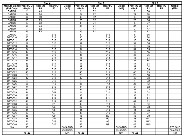
Front and Rear User I/O Mapping
Front/Rear User I/O Mapping (for reference) is shown below, with respect to DATAIO. Additional information on pin-outs can be found in the Module Operational Manuals.
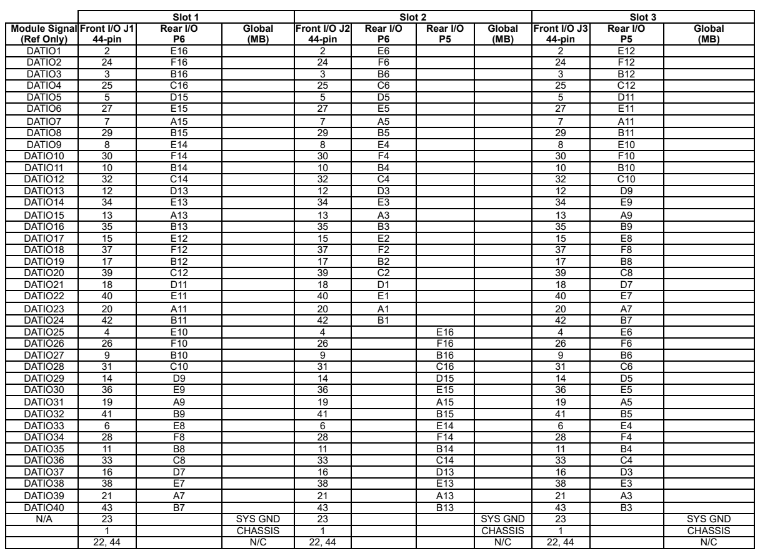
| Slot 1 | Slot 2 | Slot 3 | Module Signal (Ref Only) | Front I/O J1 44-pin | Rear I/O P6 | Global (MB) |
|---|---|---|---|---|---|---|
| Front I/O J2 44-pin | Rear I/O P6 | Rear I/O P5 | Global (MB) | Front I/O J3 44-pin | Rear I/O P5 | Global (MB) |
| DATIO1 | 2 | E16 | 2 | E6 | 2 | E12 |
| DATIO2 | 24 | F16 | 24 | F6 | 24 | F12 |
| DATIO3 | 3 | B16 | 3 | B6 | 3 | B12 |
| DATIO4 | 25 | C16 | 25 | C6 | 25 | C12 |
| DATIO5 | 5 | D15 | 5 | D5 | 5 | D11 |
| DATIO6 | 27 | E15 | 27 | E5 | 27 | E11 |
| DATIO7 | 7 | A15 | 7 | A5 | 7 | A11 |
| DATIO8 | 29 | B15 | 29 | B5 | 29 | B11 |
| DATIO9 | 8 | E14 | 8 | E4 | 8 | E10 |
| DATIO10 | 30 | F14 | 30 | F4 | 30 | F10 |
| DATIO11 | 10 | B14 | 10 | B4 | 10 | B10 |
| DATIO12 | 32 | C14 | 32 | C4 | 32 | C10 |
| DATIO13 | 12 | D13 | 12 | D3 | 12 | D9 |
| DATIO14 | 34 | E13 | 34 | E3 | 34 | E9 |
| DATIO15 | 13 | A13 | 13 | A3 | 13 | A9 |
| DATIO16 | 35 | B13 | 35 | B3 | 35 | B9 |
| DATIO17 | 15 | E12 | 15 | E2 | 15 | E8 |
| DATIO18 | 37 | F12 | 37 | F2 | 37 | F8 |
| DATIO19 | 17 | B12 | 17 | B2 | 17 | B8 |
| DATIO20 | 39 | C12 | 39 | C2 | 39 | C8 |
| DATIO21 | 18 | D11 | 18 | D1 | 18 | D7 |
| DATIO22 | 40 | E11 | 40 | E1 | 40 | E7 |
| DATIO23 | 20 | A11 | 20 | A1 | 20 | A7 |
| DATIO24 | 42 | B11 | 42 | B1 | 42 | B7 |
| DATIO25 | 4 | E10 | 4 | E16 | 4 | E6 |
| DATIO26 | 26 | F10 | 26 | F16 | 26 | F6 |
| DATIO27 | 9 | B10 | 9 | B16 | 9 | B6 |
| DATIO28 | 31 | C10 | 31 | C16 | 31 | C6 |
| DATIO29 | 14 | D9 | 14 | D15 | 14 | D5 |
| DATIO30 | 36 | E9 | 36 | E15 | 36 | E5 |
| DATIO31 | 19 | A9 | 19 | A15 | 19 | A5 |
| DATIO32 | 41 | B9 | 41 | B15 | 41 | B5 |
| DATIO33 | 6 | E8 | 6 | E14 | 6 | E4 |
| DATIO34 | 28 | F8 | 28 | F14 | 28 | F4 |
| DATIO35 | 11 | B8 | 11 | B14 | 11 | B4 |
| DATIO36 | 33 | C8 | 33 | C14 | 33 | C4 |
| DATIO37 | 16 | D7 | 16 | D13 | 16 | D3 |
| DATIO38 | 38 | E7 | 38 | E13 | 38 | E3 |
| DATIO39 | 21 | A7 | 21 | A13 | 21 | A3 |
| DATIO40 | 43 | B7 | 43 | B13 | 43 | B3 |
| N/A | 23 | SYS GND | 23 | SYS GND | 23 | SYS GND |
| 1 | CHASSIS | 1 | CHASSIS | 1 | CHASSIS | 22, 44 |
| N/C | 22, 44 | N/C | 22, 44 | N/C |
| Slot 4 | Slot 5 | Slot 6 | Module Signal (Ref Only) | Front I/O J4 44-pin | Rear I/O P4 | Rear I/O P3 |
|---|---|---|---|---|---|---|
| Global (MB) | Front I/O J5 44-pin | Rear I/O P3 | Rear I/O P2 | Global (MB) | Front I/O J6 44-pin | Rear I/O P2 |
| Rear I/O P1 | Global (MB) | DATIO1 | 2 | A1 | 2 | E2 |
| 2 | E8 | DATIO2 | 24 | B1 | 24 | F2 |
| 24 | F8 | DATIO3 | 3 | D1 | 3 | B2 |
| 3 | B8 | DATIO4 | 25 | E1 | 25 | C2 |
| 25 | C8 | DATIO5 | 5 | B2 | 5 | D1 |
| 5 | D7 | DATIO6 | 27 | C2 | 27 | E1 |
| 27 | E7 | DATIO7 | 7 | E2 | 7 | A1 |
| 7 | A7 | DATIO8 | 29 | F2 | 29 | B1 |
| 29 | B7 | DATIO9 | 8 | E16 | 8 | E16 |
| 8 | E6 | DATIO10 | 30 | F16 | 30 | F16 |
| 30 | F6 | DATIO11 | 10 | B16 | 10 | B16 |
| 10 | B6 | DATIO12 | 32 | C16 | 32 | C16 |
| 32 | C6 | DATIO13 | 12 | D15 | 12 | D15 |
| 12 | D5 | DATIO14 | 34 | E15 | 34 | E15 |
| 34 | E5 | DATIO15 | 13 | A15 | 13 | A15 |
| 13 | A5 | DATIO16 | 35 | B15 | 35 | B15 |
| 35 | B5 | DATIO17 | 15 | E14 | 15 | E14 |
| 15 | E4 | DATIO18 | 37 | F14 | 37 | F14 |
| 37 | F4 | DATIO19 | 17 | B14 | 17 | B14 |
| 17 | B4 | DATIO20 | 39 | C14 | 39 | C14 |
| 39 | C4 | DATIO21 | 18 | D13 | 18 | D13 |
| 18 | D3 | DATIO22 | 40 | E13 | 40 | E13 |
| 40 | E3 | DATIO23 | 20 | A13 | 20 | A13 |
| 20 | A3 | DATIO24 | 42 | B13 | 42 | B13 |
| 42 | B3 | DATIO25 | 4 | E12 | 4 | E12 |
| 4 | E2 | DATIO26 | 26 | F12 | 26 | F12 |
| 26 | F2 | DATIO27 | 9 | B12 | 9 | B12 |
| 9 | B2 | DATIO28 | 31 | C12 | 31 | C12 |
| 31 | C2 | DATIO29 | 14 | D11 | 14 | D11 |
| 14 | D1 | DATIO30 | 36 | E11 | 36 | E11 |
| 36 | E1 | DATIO31 | 19 | A11 | 19 | A11 |
| 19 | A1 | DATIO32 | 41 | B11 | 41 | B11 |
| 41 | B1 | DATIO33 | 6 | G1 | 6 | E10 |
| 6 | G1 | DATIO34 | 28 | G3 | 28 | F10 |
| 28 | G3 | DATIO35 | 11 | G5 | 11 | B10 |
| 11 | G5 | DATIO36 | 33 | G7 | 33 | C10 |
| 33 | G7 | DATIO37 | 16 | G9 | 16 | D9 |
| 16 | G9 | DATIO38 | 38 | G11 | 38 | E9 |
| 38 | G11 | DATIO39 | 21 | G13 | 21 | A9 |
| 21 | G13 | DATIO40 | 43 | G15 | 43 | B9 |
| 43 | G15 | N/A | 23 | SYS GND | 23 | SYS GND |
| 23 | SYS | GND | 1 | CHASSIS | 1 | CHASSIS |
| 1 | CHASSIS | 22, 44 | N/C | 22, 44 | N/C | 22, 44 |
| N/C |
High Speed I/O Modules
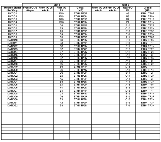
| Slot 5 | Slot 6 | Module Signal (Ref Only) | Front I/O J5 44-pin | Front I/O J5 44-pin |
|---|---|---|---|---|
| Rear I/O P3 | Global (MB) | Front I/O J6 44-pin | Front I/O J6 44-pin | Rear I/O P1 |
| Global (MB) | DATIO1 | E10 | ETH1 TP0P | A9 |
| ETH1 TP0P | DATIO2 | F10 | ETH1 TP0N | B9 |
| ETH1 TP0N | DATIO3 | B10 | ETH1 TP1P | D9 |
| ETH1 TP1P | DATIO4 | C10 | ETH1 TP1N | E9 |
| ETH1 TP1N | DATIO5 | D9 | ETH1 TP2P | B10 |
| ETH1 TP2P | DATIO6 | E9 | ETH1 TP2N | C10 |
| ETH1 TP2N | DATIO7 | A9 | ETH1 TP3P | E10 |
| ETH1 TP3P | DATIO8 | B9 | ETH1 TP3N | F10 |
| ETH1 TP3N | DATIO9 | E8 | ETH2 TP0P | A11 |
| ETH2 TP0P | DATIO10 | F8 | ETH2 TP0N | B11 |
| ETH2 TP0N | DATIO11 | B8 | ETH2 TP1P | D11 |
| ETH2 TP1P | DATIO12 | C8 | ETH2 TP1N | E11 |
| ETH2 TP1N | DATIO13 | D7 | ETH2 TP2P | B12 |
| ETH2 TP2P | DATIO14 | E7 | ETH2 TP2N | C12 |
| ETH2 TP2N | DATIO15 | A7 | ETH2 TP3P | E12 |
| ETH2 TP3P | DATIO16 | B7 | ETH2 TP3N | F12 |
| ETH2 TP3N | DATIO17 | E6 | ETH3 TP0P | A13 |
| ETH3 TP0P | DATIO18 | F6 | ETH3 TP0N | B13 |
| ETH3 TP0N | DATIO19 | B6 | ETH3 TP1P | D13 |
| ETH3 TP1P | DATIO20 | C6 | ETH3 TP1N | E13 |
| ETH3 TP1N | DATIO21 | D5 | ETH3 TP2P | B14 |
| ETH3 TP2P | DATIO22 | E5 | ETH3 TP2N | C14 |
| ETH3 TP2N | DATIO23 | A5 | ETH3 TP3P | E14 |
| ETH3 TP3P | DATIO24 | B5 | ETH3 TP3N | F14 |
| ETH3 TP3N | DATIO25 | E4 | ETH4 TP0P | A15 |
| ETH4 TP0P | DATIO26 | F4 | ETH4 TP0N | B15 |
| ETH4 TP0N | DATIO27 | B4 | ETH4 TP1P | D15 |
| ETH4 TP1P | DATIO28 | C4 | ETH4 TP1N | E15 |
| ETH4 TP1N | DATIO29 | D3 | ETH4 TP2P | B16 |
| ETH4 TP2P | DATIO30 | E3 | ETH4 TP2N | C16 |
| ETH4 TP2N | DATIO31 | A3 | ETH4 TP3P | E16 |
| ETH4 TP3P | DATIO32 | B3 | ETH4 TP3N | F16 |
| ETH4 TP3N |
Ethernet (Rear I/O)
Commercial Equivalent RJ45-type Ethernet cabling/wiring (for reference only):
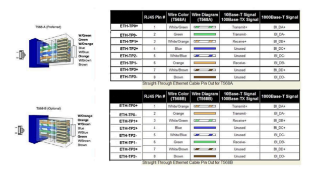
Connector Signal/Pinout Notes
NAI Synchro/Resolver Naming Convention
| Signal | Resolver | Synchro |
|---|---|---|
| S1 | SIN(-) | X |
| S2 | COS(+) | Z |
| S3 | SIN(+) | Y |
| S4 | COS(-) | No connect |
Additional Pinout Notes
| 1. Isolated Discrete Module (DT2) |
|---|
| For ‘differential’ A/D; “P” designation considered ‘positive’ input pin, “N” pin designation considered ‘negative’ input pin. |
| 2. Discrete I/O Module (DT1) |
| All GND pins are common within the module, but, isolated from system/power GND. Each pin should be individually wired for optimal power current distribution. |
| 3. TTL I/O Module (TL1) |
| I/O referenced to system power GND. |
| 4. CMRP - A/D Module(s) (ADx) |
| The Common Mode Reference Point (CMRP) is an isolated reference connection for all the A/D channels. For expected high common mode voltage applications, it is recommended that the pin designated as CMRP be referenced (direct or resistor coupled) to the signal source GND reference (must have current path between CMRP and signal source generator) to minimize common mode voltage within the acceptable specification range. All channels within the module are independent but share a CMRP, which is isolated from system/power GND. |
MECHANICAL DETAILS
General - Outline
Note
The following mechanical outline detail examples are provided for reference only. Dimensions are in inches unless otherwise specified.
Conduction Cooled
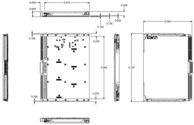
Outline, General, Conduction Cooled
Convection Cooled
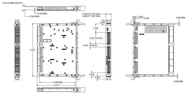
Outline, General, Convection Cooled
67G6 PART NUMBER DESIGNATION
Click here for the 67G6 part number designation
SYNCHRO/RESOLVER AND LVDT/RVDT SIMULATION MODULE CODE TABLES
Select the Digital-to-Synchro (DSx), Digital-to-Resolver (DRx) or Digital-to-LVDT/RVDT (DLx) module ID corresponding to the application operating parameters required from the following code table (where x = the specific module ID designator). Customer should indicate the actual frequency applicable the design to assure that the correct default band width is set at the factory. All Input and Reference voltages are auto ranging. Frequency/voltage band tolerances +/- 10%. For availability and ranges other than those listed contact the factory. Specifications may be subject to change.
- Single Channel module pending availability (contact factory)
Module ID Format Channel(s) Output Voltage VL-L (Vrms) Reference Voltage (Vrms) Frequency Range (Hz) Power / CH maximum (VA) Notes DS1 SYN 1* 2 - 28 2 - 115 47 - 1 K 3 DR1 RSL DL1 LVDT/RVDT DS2 SYN 1* 2 - 28 2 - 115 1 K - 5 K 3 DR2 RSL DL2 LVDT/RVDT DS3 SYN 1* 2 - 28 2 - 115 5 K - 10 K 3 DR3 RSL DL3 LVDT/RVDT DS4 SYN 1* 2 - 28 2 - 115 10 K - 20 K 3 DR4 RSL DL4 LVDT/RVDT DS5 SYN 1* 28 - 90 2 - 115 47 - 1 K 3 DR5 RSL DL5 LVDT/RVDT DSX SYN 1* X X X X X = TBD; special configuration, requires special part number code designation, contact factory DRX RSL DLX LVDT/RVDT DSA SYN 2 2 - 28 2 - 115 47 - 1 K 1.5 DRA RSL DLA LVDT/RVDT DSB SYN 2 2 - 28 2 - 115 1 K - 5 K 1.5 DRB RSL DLB LVDT/RVDT DSC SYN 2 2 - 28 2 - 115 5 K - 10 K 1.5 DRC RSL DLC LVDT/RVDT DSD SYN 2 2 - 28 2 - 115 10 K - 20 K 1.5 DRD RSL DLD LVDT/RVDT DSE SYN 2 28 - 90 2 - 115 47 - 1 K 2.2 DRE RSL DLE LVDT/RVDT DSY SYN 2 Y Y Y Y Y = TBD; special configuration, requires special part number code designation, contact factory DRY RSL DLY LVDT/RVDT DSJ SYN 3 2 - 28 2 - 115 47 - 1 K 0.5 DRJ RSL DLJ LVDT/RVDT DSK SYN 3 2 - 28 2 - 115 1 K - 5 K 0.5 DRK RSL DLK LVDT/RVDT DSL SYN 3 2 - 28 2 - 115 5 K - 10 K 0.5 DRL RSL DLL LVDT/RVDT DSM SYN 3 2 - 28 2 - 115 10 K - 20 K 0.5 DRM RSL DLM LVDT/RVDT DSN SYN 3 28 - 90 2 - 115 47 - 1 K 0.5 DRN RSL DLN LVDT/RVDT DSZ SYN 3 Z Z Z Z Z = TBD; special configuration, requires special part number code designation, contact factory DRZ RSL DLZ LVDT/RVDT SYNCHRO/RESOLVER AND LVDT/RVDT MEASUREMENT MODULE CODE TABLES
SYN/RSL Four-Channel Measurement (Field Programmable SYN/RSL)
Select the Synchro/Resolver-to-Digital (SDx) module ID corresponding to the application operating parameters required from the following code table (where x = the specific module ID designator). Customer should indicate the actual frequency applicable to the design to assure that the correct default band width is set at the factory. All Input and Reference voltages are auto ranging. For availability and ranges other than those listed contact the factory. Specifications may be subject to change.
Frequency/voltage band tolerances +/- 10%.
Module ID Input Voltage V (Vrms) Reference Voltage + (Vrms) Frequency Range + (Hz) Notes SD1 2 - 28 2 - 115 47 - 1 K SD2 2 - 28 2 - 115 1K - 5 K SD3 2 - 28 2 - 115 5K - 10 K SD4* 2 - 28 2 - 115 10K - 20 K SD5 28 - 90 2 - 115 47 - 1 K SDX* X X X X = TBD; special configuration, requires special part number code designation, contact factory *Consult factory for availability
LVDT/RVDT Four-Channel Measurement (Field Programmable 2, 3 or 4-Wire)
Select the LVDT/RVDT-to-Digital (LDx) module ID corresponding to the application operating parameters required from the following code table (where x = the specific module ID designator). Customer should indicate the actual frequency applicable to the design to assure that the correct default band width is set at the factory. All Input and Excitation voltages are auto ranging. For availability and ranges other than those listed contact the factory. Specifications may be subject to change.
Frequency/voltage band tolerances +/- 10%.
Module ID Input Signal Voltage V + (Vrms) Excitation Voltage + (Vrms) Frequency Range + (Hz) Notes LD1 2 - 28 2 - 115 47 - 1 K LD2 2 - 28 2 - 115 1K - 5 K LD3 2 - 28 2 - 115 5K - 10 K LD4* 2 - 28 2 - 115 10K - 20 K LD5 28 - 90 2 - 115 47 - 1 K LDX* X X X X = TBD; special configuration, requires special part number code designation, contact factory *Consult factory for availability
Link to original
ONBOARD DISCRETE INPUT/OUTPUT OPTION
In addition to its extensive modular configurability (up to six NAI smart I/O and communications function modules), the 67G6 is also designed to offer a seventh I/O function that is directly embedded on the motherboard. This ‘onboard’ option enables the 67G6 to provide either 24 channels of Standard Function (SF) Discrete I/O (like NAI’s DT1 module) or 24 channels of Enhanced Function (EF) Discrete I/O (like NAI’s DT4 module). As a result, the 67G6 offers additional functionality and versatility while still maintaining a 6U OpenVPX profile.
Principle of Operation
The Onboard Discrete Input/Output Option provides up to 24 individual digital I/O channels with BIT fault detection, which enables flagging of noncompliant outputs or inconsistent input readings between dual input measurements.
When channels are programmed as inputs, they can be used for either voltage or contact sensing. Channels set for contact sensing (e.g. sensing a relay contact position; OPEN-CLOSED) can be configured with a programmable “pull-up” or “pull-down” (current source or sink) which effectively provides the proper voltage level change to sense the open state of the contact. This unique design eliminates the need for external resistors or mechanical jumpers. Instead, this design offers a current source/sink (in banks of 6 channels) that the user programs to a desired current (0-5 mA) level.
When programmed as outputs, each channel can be set for high-side (current-source), low-side (current-sink) or push-pull (current-source-sink) operation. The load impedance determines the delivered switched output current drive - up to 500 mA per channel. Diode clamping is provided (useful for inductive loads, such as relays) and thermal protection.
Overcurrent protection is implemented using current sensing technology. When the current exceeds a programmed threshold of 650 mA steady-state, or a higher short duration, the overcurrent/short-circuit protection is triggered, shutting down the output drivers for safety. The overcurrent fault status will be indicated for the affected channels and will require a reset operation to restore output. To reset this condition, a reset command needs to be issued to the Overcurrent Reset register, which will restore drive output and allow the latched status to be reset. This is separate from the reset for the Overcurrent Interrupt Enable register on this module. It is recommended that a reset command is done whenever status is cleared to avoid a non-apparent output reset condition.
The 24 channels are configured as 4 banks of 6 channels. Each bank is provided with a separate external input VCC and a ground return (GND) pin. The GND pins are common within the module but are isolated from system (power) GND.
Operational requirements/assumptions:
- An external source VCC supply must be wired for proper:
- Output operation as a current source.
- Input operation when requiring a programmed pull-up current (i.e. programmed “pull-up” for input contact sense; OPEN/GND detect/state change).
- An external source Ground/Return must be wired for all I/O configurations. The Ground/Return must be the input signal or the load current sink ground/reference.
Input/Output Interface
Each channel can be configured as an input or one of three types of outputs.
Output
When configured as an output, the interface can act as a “High-Side”, “Low-Side” or “Push-Pull” drive, providing up to 500 mA per channel or 1 A when two channels are connected in parallel. The total output per module is 8 A (2 A per bank).
Note
Maximum source current ‘rules’ for rear I/O connectors still apply - see specifications.
Input
When configured as an input, output drivers are disabled. The I/O interface can act as a constant current source, current sink or voltage sensing circuit. For contact sensing, each channel may be set for pull-up or pull-down using the Select Pull-Up or Pull-Down register and by entering the appropriate current level in the Pull-Up/Down Current register. Contact closure and hysteresis may be defined using the Upper Voltage and Lower Voltage Threshold registers. No additional resistors or hardware are required to provide for current flow. A current value of zero disables the current source/sink circuits and configures the module for voltage sensing. Default is voltage sensing. Level or contact sensing can be mixed within a channel bank if the contact sensing channels are externally pulled up or pulled down.
Note
If this module supplies the current for the contact sensing, then level and contact sensing cannot be mixed within a channel bank.
All four threshold levels must be programmed in monotonic, increasing order of: Minimum Low, Lower, Upper and Maximum High. For input and output, threshold levels define logic state. For output, threshold levels are used in BIT test (wrap-around) signal monitoring. A pair of drive FETs and current circuits are provided at each I/O pin. See the functional representation of the drivers in the I/O Circuits interface diagram below.
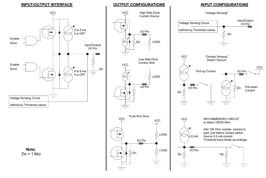
Discrete Input/Output Voltage Threshold Programming
Four threshold levels: Max High Voltage Threshold, Upper Voltage Threshold, Lower Voltage Threshold, and Min Low Voltage Threshold offer maximum user flexibility. All four threshold levels must be programmed. For input or output, the threshold levels will define the logic states. For proper operation, the threshold values should be programmed such that:
Max High Voltage Threshold > Upper Voltage Threshold > Lower Voltage Threshold > Min Low Voltage Threshold
Program Upper and Lower Voltage Thresholds, keeping the 0.25 V min. differential in mind, and then add debounce time as required. When the input signal exceeds the Upper Voltage Threshold, a logic high 1 is maintained until the input signal falls below the Lower Voltage Threshold. Conversely, when the input signal falls below the Lower Voltage Threshold, a logic low 0 is maintained until the input signal rises above the Upper Voltage Threshold.
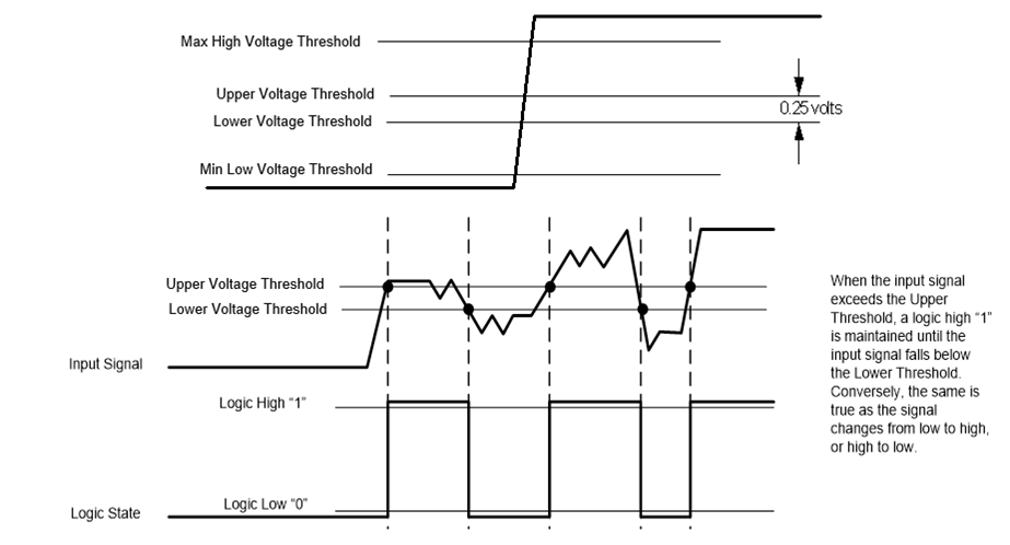
Debounce Programming
The Debounce register, when programmed for a non-zero value, is used with channels programmed as input to “filter” or “ignore” expected application spurious initial transitions. Once a signal level is a logic voltage level period longer than the Debounce Time (Logic High and Logic Low), a logic transition is validated. Signal pulse widths less than programmed Debounce Time are filtered. Once valid, the transition status register flag is set for the channel and the output logic changes state.
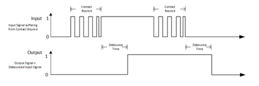
Automatic Background Built-In Test (BIT)/Diagnostic Capability
The On-Board Discrete Input/Output Option supports automatic background BIT testing that verifies channel processing. The testing is totally transparent to the user, requires no external programming and has no effect on the operation of the module. This capability is accomplished by an additional test comparator that is incorporated into each module. The test comparator checks each channel and is compared against the operational channel. Depending upon the configuration, the Input data read, or Output logic written of the operational channel and test comparator must agree or a fault is indicated with the results available in the associated status register. The results of the tests are stored in the BIT Dynamic Status and BIT Latched Status registers.
The technique used by the continuous background BIT (CBIT) test consists of an “add-2, subtract-1” counting scheme. The BIT counter is incremented by 2 when a BIT-fault is detected and decremented by 1 when there is no BIT fault detected and the BIT counter is greater than 0. When the BIT counter exceeds the (programmed) Background BIT Threshold value, the specific channel’s fault bit in the BIT status register will be set. Note, the interval at which BIT is performed is dependent and differs between module types. Rather than specifying the BIT Threshold as a “count”, the BIT Threshold is specified as a time in milliseconds. The module will convert the time specified to the BIT Threshold “count” based on the BIT interval for that module. The “add-2, subtract-1” counting scheme effectively filters momentary or intermittent anomalies by allowing them to “come and go“ before a BIT fault status or indication is flagged (e.g. BIT faults would register when sustained; i.e. at a ten second interval, not a 10-millisecond interval). This prevents spurious faults from registering valid such as those caused by EMI and/or dirty power causing false BIT faults. Putting more “weight” on errors (“add-2”) and less “weight” on subsequent passing results (subtract-1) will result in a BIT failure indication even if a channel “oscillates” between a pass and fail state.
In addition to BIT, the On-Board Discrete Input/Output Option tests for overcurrent conditions and provides Above Max High Voltage, Below Min Low Voltage, and Mid-Range Voltage statuses for threshold signal transitioning.
Status and Interrupts
The On-Board Discrete Input/Output Option provide registers that indicate faults or events. Refer to Appendix A: Status and Interrupts for the Principle of Operation description.
Unit Conversions
The Discrete I/O Threshold and Measurement registers can be programmed to be utilized as a single precision floating point value (IEEE-754) or as a 32-bit integer value. The purpose for providing this feature is to offload the processing that is normally performed by the mission processor to convert the integer values to floating-point values.
When the Enable Floating Point Mode register is set to 1 (Floating Point Mode) the following registers are formatted as Single Precision Floating Point Value (IEEE-754):
- Voltage Reading (Volts)
- Current Reading (mA)
- VCC Voltage Reading (Volts)
- Max High Voltage Threshold (Volts)*
- Upper Voltage Threshold (Volts)*
- Lower Voltage Threshold (Volts)*
- Min Low Voltage Threshold (Volts)*
- Pull-Up/Down Current (mA)*
*When the Enable Floating Point Mode register is set to 1, it is important that these registers are updated with the Single Precision Floating Point (IEEE-754) representation of the value for proper operation of the channel. Conversely, when the Enable Floating Point Mode register is set to 0, these registers must be updated with the Integer 32-bit representation of the value.
Note
when changing the Enable Floating Point Mode from Integer Mode to Floating Point Mode or vice versa, the following steps are followed to avoid faults from falsely being generated:
-
Set the Enable Floating Point Mode register to the desired mode (Integer or Floating Point).
-
The application waits for the Floating Point State register to match the value for the requested Floating Point Mode (Integer = 0, Floating Point = 1); this indicates that the module’s conversion of the register values and internal values is complete. Data registers will be converted to the units specified and can be read in that specified format.
User Watchdog Timer Capability
The On-Board Discrete Input/Output Option provide registers that support User Watchdog Timer capability. Refer to Appendix B: User Watchdog Timer Functionality for the Principle of Operation description.
Enhanced Functionality Option
The On-Board Discrete Input/Output Option offers a separate option for enhanced input and output mode functionality. For incoming signals (inputs), the enhanced modes include Pulse Measurements, Transition Timestamps, Transition Counters, Period Measurement and Frequency Measurement. For outputs, the enhanced modes include PWM (Pulse Width Modulation) Outputs and Pattern Generator Outputs.
Refer to Appendix C: Enhanced Input/Output Functionality for the Principle of Operation description.
Register Descriptions
The register descriptions provide the Register Name, Type, Data Range, Read or Write information, power on default initialized values, a description of the function and a data table where applicable,
Discrete Input/Output Registers
Each channel can be configured as an input or one of three types of outputs. The I/O Format (Ch1-16 and Ch17-24) registers are used to set each channel input/output configuration. The Write Outputs register controls the output channels to either a High (1) or Low (0) state, and the Read I/O register contains the discrete channel’s state (High (1) or Low (0)) as specified by the channel’s threshold configurations.
I/O Format Ch1-16
Function: Sets channels 1-16 as inputs or outputs. See I/O Format Ch17-24 register for channels 17-24.
Type: unsigned binary word (32-bit)
Data Range: 0x0000 0000 to 0xFFFF FFFF
Read/Write: R/W
Initialized Value: 0
Operational Settings: Write integer 0 for input; 1, 2 or 3 for specific output format.
| Integer | DH | DL | (2 bits per channel) |
|---|---|---|---|
| 0 | 0 | 0 | Input |
| 1 | 0 | 1 | Output, Low-side switched, with/without current pull up |
| 2 | 1 | 0 | Output, High-side switched, with/without current pull down |
| 3 | 1 | 1 | Output, push-pull |
I/O Format Ch1-16
| D31 | D30 | D29 | D28 | D27 | D26 | D25 | D24 | D23 | D22 | D21 | D20 | D19 | D18 | D17 | D16 |
| Ch16 | Ch15 | Ch14 | Ch13 | Ch12 | Ch11 | Ch10 | Ch9 | ||||||||
| D15 | D14 | D13 | D12 | D11 | D10 | D9 | D8 | D7 | D6 | D5 | D4 | D3 | D2 | D1 | D0 |
| Ch8 | Ch7 | Ch6 | Ch5 | Ch4 | Ch3 | Ch2 | Ch1 | ||||||||
I/O Format Ch17-24
Function: Sets channels 17-24 as inputs or outputs. See I/O Format Ch1-16 for channels 1-16.
Type: unsigned binary word (32-bit)
Data Range: 0x0000 0000 to 0x0000 FFFF
Read/Write: R/W
Initialized Value: 0
Operational Settings: Write integer 0 for input; 1, 2 or 3 for specific output format.
| Integer | DH | DL | (2 bits per channel) |
|---|---|---|---|
| 0 | 0 | 0 | Input |
| 1 | 0 | 1 | Output, Low-side switched, with/without current pull up |
| 2 | 1 | 0 | Output, High-side switched, with/without current pull down |
| 3 | 1 | 1 | Output, push-pull |
I/O Format Ch17-24
| D31 | D30 | D29 | D28 | D27 | D26 | D25 | D24 | D23 | D22 | D21 | D20 | D19 | D18 | D17 | D16 |
| 0 | 0 | 0 | 0 | 0 | 0 | 0 | 0 | 0 | 0 | 0 | 0 | 0 | 0 | 0 | 0 |
| D15 | D14 | D13 | D12 | D11 | D10 | D9 | D8 | D7 | D6 | D5 | D4 | D3 | D2 | D1 | D0 |
| Ch24 | Ch23 | Ch22 | Ch21 | Ch20 | Ch19 | Ch18 | Ch17 | ||||||||
Write Outputs
Function: Drives output channels High 1 or Low 0
Type: unsigned binary word (32-bit)
Data Range: 0x0000 0000 to 0x00FF FFFF
Read/Write: R/W
Initialized Value: 0
Operational Settings: Write 1 to drive output high. Write 0 to drive output low.
Write Outputs
| D31 | D30 | D29 | D28 | D27 | D26 | D25 | D24 | D23 | D22 | D21 | D20 | D19 | D18 | D17 | D16 |
|---|---|---|---|---|---|---|---|---|---|---|---|---|---|---|---|
| 0 | 0 | 0 | 0 | 0 | 0 | 0 | 0 | Ch24 | Ch23 | Ch22 | Ch21 | Ch20 | Ch19 | Ch18 | Ch17 |
| D15 | D14 | D13 | D12 | D11 | D10 | D9 | D8 | D7 | D6 | D5 | D4 | D3 | D2 | D1 | D0 |
| Ch16 | Ch15 | Ch14 | Ch13 | Ch12 | Ch11 | Ch10 | Ch9 | Ch8 | Ch7 | Ch6 | Ch5 | Ch4 | Ch3 | Ch2 | Ch1 |
Input/Output State
Function: Reads High 1 or Low 0 inputs or outputs as defined by internal channel threshold values.
Type: unsigned binary word (32-bit)
Data Range: 0x0000 0000 to 0x00FF FFFF
Read/Write: R
Initialized Value: N/A
Operational Settings: Bit-mapped per channel.
Input/Output State
| D31 | D30 | D29 | D28 | D27 | D26 | D25 | D24 | D23 | D22 | D21 | D20 | D19 | D18 | D17 | D16 |
|---|---|---|---|---|---|---|---|---|---|---|---|---|---|---|---|
| 0 | 0 | 0 | 0 | 0 | 0 | 0 | 0 | Ch24 | Ch23 | Ch22 | Ch21 | Ch20 | Ch19 | Ch18 | Ch17 |
| D15 | D14 | D13 | D12 | D11 | D10 | D9 | D8 | D7 | D6 | D5 | D4 | D3 | D2 | D1 | D0 |
| Ch16 | Ch15 | Ch14 | Ch13 | Ch12 | Ch11 | Ch10 | Ch9 | Ch8 | Ch7 | Ch6 | Ch5 | Ch4 | Ch3 | Ch2 | Ch1 |
Discrete Input/Output Threshold Programming Registers
Four threshold levels: Max High Voltage Threshold, Upper Voltage Threshold, Lower Voltage Threshold, and Min Low Voltage Threshold are programmable for each Discrete channel in the module.
| Max High Voltage Threshold (Enable Floating Point Mode: Integer Mode) | |||||||||||||||
| Upper Voltage Threshold (Enable Floating Point Mode: Integer Mode) | |||||||||||||||
| Lower Voltage Threshold (Enable Floating Point Mode: Integer Mode) | |||||||||||||||
| Min Low Voltage Threshold (Enable Floating Point Mode: Integer Mode) | |||||||||||||||
| D31 | D30 | D29 | D28 | D27 | D26 | D25 | D24 | D23 | D22 | D21 | D20 | D19 | D18 | D17 | D16 |
| 0 | 0 | 0 | 0 | 0 | 0 | 0 | 0 | 0 | 0 | 0 | 0 | 0 | 0 | 0 | 0 |
| D15 | D14 | D13 | D12 | D11 | D10 | D9 | D8 | D7 | D6 | D5 | D4 | D3 | D2 | D1 | D0 |
| 0 | 0 | 0 | D | D | D | D | D | D | D | D | D | D | D | D | D |
| Max High Voltage Threshold (Enable Floating Point Mode: Floating Point Mode) | |||||||||||||||
| Upper Voltage Threshold (Enable Floating Point Mode: Floating Point Mode) | |||||||||||||||
| Lower Voltage Threshold (Enable Floating Point Mode: Floating Point Mode) | |||||||||||||||
| Min Low Voltage Threshold (Enable Floating Point Mode: Floating Point Mode) | |||||||||||||||
| D31 | D30 | D29 | D28 | D27 | D26 | D25 | D24 | D23 | D22 | D21 | D20 | D19 | D18 | D17 | D16 |
| D | D | D | D | D | D | D | D | D | D | D | D | D | D | D | D |
| D15 | D14 | D13 | D12 | D11 | D10 | D9 | D8 | D7 | D6 | D5 | D4 | D3 | D2 | D1 | D0 |
| 0 | 0 | 0 | D | D | D | D | D | D | D | D | D | D | D | D | D |
Max High Voltage Threshold
Function: Sets the maximum high voltage threshold value. Programmable per channel from 0 VDC to 60 VDC.
Type: unsigned binary word (32-bit) (Integer Mode) or Single Precision Floating Point Value (IEEE-754) (Floating Point Mode)
Data Range:
Enable Floating Point Mode: 0 (Integer Mode)
0x0000 0000 to 0x0000 0258
Enable Floating Point Mode: 1 (Floating Point Mode)
Single Precision Floating Point Value (IEEE-754)
Read/Write: R/W
Initialized Value: 0x32
Operational Settings: Assumes that the programmed level is the minimum voltage used to indicate a Max High Voltage Threshold. If a signal is greater than the Max High Voltage Threshold value, a flag is set in the Max High Voltage Threshold Status register. The Max High Voltage Threshold register may be used to monitor any type of high signal voltage condition or threshold such as a “Short to +V” as it applies to input measurement as well as contact sensing applications.
Integer Mode: LSB is 0.1 VDC. For example: to program 5.0 VDC, 5.0 / 0.1 = 50 (binary equivalent for 50 is 0x0000 0032).
Floating Point Mode: Set Max High Voltage Threshold value as a Single Precision Floating Point Value (IEEE-754). For example, to program 5.0 V, enter 5.0 as a single precision floating point value (IEEE-754) (binary equivalent 5.0 is 0x40A0 0000).
Upper Voltage Threshold
Function: Sets the upper voltage threshold value. Programmable per channel from 0 VDC to 60 VDC.
Type: unsigned binary word (32-bit) (Integer Mode) or Single Precision Floating Point Value (IEEE-754) (Floating Point Mode)
Data Range:
Enable Floating Point Mode: 0 (Integer Mode)
0x0000 0000 to 0x0000 0258
Enable Floating Point Mode: 1 (Floating Point Mode)
Single Precision Floating Point Value (IEEE-754)
Read/Write: R/W
Initialized Value: 0x28
Operational Settings: A signal is considered logic High 1 when its value exceeds the Upper Voltage Threshold and does not consequently fall below the Upper Voltage Threshold in less than the programmed Debounce Time.
Integer Mode: LSB is 0.1 VDC. For example: to program 3.5 VDC, 3.5 / 0.1 = 35 (binary equivalent for 35 is 0x0000 0023).
Floating Point Mode: Set Upper Voltage Threshold value as a Single Precision Floating Point Value (IEEE-754). For example, to program 3.5 V, enter 3.5 as a single precision floating point value (IEEE-754) (binary equivalent 3.5 is 0x4060 0000).
Lower Voltage Threshold
Function: Sets the lower voltage threshold value. Programmable per channel from 0 VDC to 60 VDC.
Type: unsigned binary word (32-bit) (Integer Mode) or Single Precision Floating Point Value (IEEE-754) (Floating Point Mode)
Data Range:
Enable Floating Point Mode: 0 (Integer Mode)
0x0000 0000 to 0x0000 0258
Enable Floating Point Mode: 1 (Floating Point Mode)
Single Precision Floating Point Value (IEEE-754)
Read/Write: R/W
Initialized Value: 0x10
Operational Settings: A signal is considered logic Low 0 when its value falls below the Lower Voltage Threshold and does not consequently rise above the Lower Voltage Threshold in less than the programmed Debounce Time.
Integer Mode: LSB is 0.1 VDC. For example: to program 1.5 VDC, 1.5 / 0.1 = 15 (binary equivalent for 15 is 0x0000 000F).
Floating Point Mode: Set Lower Voltage Threshold value as a Single Precision Floating Point Value (IEEE-754). For example, to program 1.5 V, enter 1.5 as a single precision floating point value (IEEE-754) (binary equivalent 1.5 is 0x3FC0 0000).
Min Low Voltage Threshold
Function: Sets the minimum low voltage threshold. Programmable per channel 0 VDC to 60 VDC.
Type: unsigned binary word (32-bit) (Integer Mode) or Single Precision Floating Point Value (IEEE-754) (Floating Point Mode)
Data Range:
Enable Floating Point Mode: 0 (Integer Mode)
0x0000 0000 to 0x0000 0258
Enable Floating Point Mode: 1 (Floating Point Mode)
Single Precision Floating Point Value (IEEE-754)
Read/Write: R/W
Initialized Value: 0xA
Operational Settings: Assumes that the programmed level is the voltage used to indicate a Minimum Low Voltage Threshold. If a signal is less than the Min Low Voltage Threshold value, a flag is set in the Min Low Voltage Threshold Status register. The Min Low Voltage Threshold register may be used to monitor any type of low signal voltage condition or threshold such as a “Short to Ground” as it applies to input measurement as well as contact sensing applications.
Integer Mode: LSB is 0.1 VDC. For example: to program 0.5 VDC, 0.5 / 0.1 = 5 (binary equivalent for 5 is 0x0000 0005).
Floating Point Mode: Set Min Low Voltage Threshold value as a Single Precision Floating Point Value (IEEE-754). For example, to program 0.5 V, enter 0.5 as a single precision floating point value (IEEE-754) (binary equivalent 0.5 is 0x3F00 0000).
Discrete Input/Output Measurement Registers
The measured voltage at the I/O pin for each channel can be read from the Voltage Reading register.
Voltage Reading
Function: Reads actual voltage at I/O pin per individual channel.
Type: unsigned binary word (32-bit) (Integer Mode) or Single Precision Floating Point Value (IEEE-754) (Floating Point Mode) Data Range:
Enable Floating Point Mode: 0 (Integer Mode)
0x0000 0000 to 0x0000 0258
Enable Floating Point Mode: 1 (Floating Point Mode)
Single Precision Floating Point Value (IEEE-754)
Read/Write: R
Initialized Value: N/A
Operational Settings:
Integer Mode: LSB is 0.1 VDC. If the register value is 261 (binary equivalent for 261 is 0x0000 0105), conversion to the voltage value is 261 * 0.1 = 26.1 V.
Floating Point Mode: Read as a Single Precision Floating Point Value (IEEE-754). For example, if the register value is 0x41D0 CCCD, this is equivalent to is 26.1, which represent 26.1 V.
Voltage Reading (Enable Floating Point Mode: Integer Mode)
| D31 | D30 | D29 | D28 | D27 | D26 | D25 | D24 | D23 | D22 | D21 | D20 | D19 | D18 | D17 | D16 |
|---|---|---|---|---|---|---|---|---|---|---|---|---|---|---|---|
| 0 | 0 | 0 | 0 | 0 | 0 | 0 | 0 | 0 | 0 | 0 | 0 | 0 | 0 | 0 | 0 |
| D15 | D14 | D13 | D12 | D11 | D10 | D9 | D8 | D7 | D6 | D5 | D4 | D3 | D2 | D1 | D0 |
| D | D | D | D | D | D | D | D | D | D | D | D | D | D | D | D |
Voltage Reading (Enable Floating Point Mode: Floating Point Mode)
| D31 | D30 | D29 | D28 | D27 | D26 | D25 | D24 | D23 | D22 | D21 | D20 | D19 | D18 | D17 | D16 |
|---|---|---|---|---|---|---|---|---|---|---|---|---|---|---|---|
| D | D | D | D | D | D | D | D | D | D | D | D | D | D | D | D |
| D15 | D14 | D13 | D12 | D11 | D10 | D9 | D8 | D7 | D6 | D5 | D4 | D3 | D2 | D1 | D0 |
| D | D | D | D | D | D | D | D | D | D | D | D | D | D | D | D |
Current Reading
Function: Reads actual output current through I/O pin per channel.
Type: signed binary word (32-bit (only lower 16-bit is used)) (Integer Mode) or Single Precision Floating Point Value (IEEE-754) (Floating Point Mode)
Data Range:
Enable Floating Point Mode: 0 (Integer Mode)
 (2's compliment. 16-bit value sign extended to 32 bits)

 0x0000 0000 to 0x0000 00D0 (positive) or 0x0000 FF30 (negative)
Enable Floating Point Mode: 1 (Floating Point Mode)
Single Precision Floating Point Value (IEEE-754)
Read/Write: R
Initialized Value: N/A
Operational Settings:
Integer Mode: LSB is 3.0 mA. Value is signed binary 16-bit word. Read as 2’s complement value for positive and negative current readings. For example, if the register value is 50 (binary equivalent for 50 is 0x0000 0032), the conversion to the current value is 50 * 3.0 = 150 mA. If register value is -50 (binary equivalent for -150 is 0x0000 FFCE), the conversion to the current value is -50 * 3.0 = -150 mA.
Floating Point Mode: Read as a Single Precision Floating Point Value (IEEE-754). The value will represent a positive or negative current reading. For example, if the register value is 0x4316 0000, this is equivalent to 150, which represent 150 mA. If the register value is 0xC316 0000, this is equivalent to -150, which represents -150 mA.
Current Reading (Enable Floating Point Mode: Integer Mode)
| D31 | D30 | D29 | D28 | D27 | D26 | D25 | D24 | D23 | D22 | D21 | D20 | D19 | D18 | D17 | D16 |
|---|---|---|---|---|---|---|---|---|---|---|---|---|---|---|---|
| 0 | 0 | 0 | 0 | 0 | 0 | 0 | 0 | 0 | 0 | 0 | 0 | 0 | 0 | 0 | 0 |
| D15 | D14 | D13 | D12 | D11 | D10 | D9 | D8 | D7 | D6 | D5 | D4 | D3 | D2 | D1 | D0 |
| D | D | D | D | D | D | D | D | D | D | D | D | D | D | D | D |
Current Reading (Enable Floating Point Mode: Floating Point Mode)
| D31 | D30 | D29 | D28 | D27 | D26 | D25 | D24 | D23 | D22 | D21 | D20 | D19 | D18 | D17 | D16 |
|---|---|---|---|---|---|---|---|---|---|---|---|---|---|---|---|
| D | D | D | D | D | D | D | D | D | D | D | D | D | D | D | D |
| D15 | D14 | D13 | D12 | D11 | D10 | D9 | D8 | D7 | D6 | D5 | D4 | D3 | D2 | D1 | D0 |
| D | D | D | D | D | D | D | D | D | D | D | D | D | D | D | D |
VCC Bank Registers
There are four VCC banks where each bank controls 6 discrete channels. Configuration for each bank involves specifying if the bank is configured for pull-up or pull-down and the current for source/sink. The measured voltage for VCC can be read from the VCC Voltage Reading register.
Select Pull-Up or Pull-Down
Function: Configures Pull-up or Pull-down configuration per 6-channel bank
Type: unsigned binary word (32-bit)
Data Range: 0 to 0x0000 000F
Read/Write: R/W
Initialized Value: 0
Operational Settings: Set bit to 1 to configure channel bank to Pull-up. Set bit to 0 to configure channel bank to Pull-down. Each data bit configures entire bank of 6 channels.
Note
For contact (switch closure) applications, a current supply (Vcc) is required for internal pull-up.
Select Pull-Up or Pull-Down
| Bit(s) | Name | Description |
|---|---|---|
| D31:D4 | Reserved | Set Reserved bits to 0. |
| D3 | Configure Bank 4 (Ch 19-24) | 1=Pull-Up, 0=Pull-Down |
| D2 | Configure Bank 3 (Ch 13-18) | 1=Pull-Up, 0=Pull-Down |
| D1 | Configure Bank 2 (Ch 07-12) | 1=Pull-Up, 0=Pull-Down |
| D0 | Configure Bank 1 (Ch 01-06) | 1=Pull-Up, 0=Pull-Down |
Pull-Up/Down Current
Function: Sets current for pull-up/down per 6-channel bank. Programmable from 0 to 5 mA.
Type: unsigned binary word (32-bit) (Integer Mode) or Single Precision Floating Point Value (IEEE-754) (Floating Point Mode)
Data Range:
Enable Floating Point Mode: 0 (Integer Mode)
0x0000 0000 to 0x0000 0032
Enable Floating Point Mode: 1 (Floating Point Mode)
Floating Point Value (IEEE-754)
Read/Write: R/W
Initialized Value: 0
Operational Settings: A current of zero disables the current pull-down circuits and configures for voltage sensing.
Integer Mode: LSB is 0.1 mA. For example: to program 5 mA, 5 / 0.1 = 50 (binary equivalent for 50 is 0x0000 0032).
Floating Point Mode: Set the current for pull-up/down as a Single Precision Floating Point Value (IEEE-754). For example, to program 5 mA, enter 5.0 as a Single Precision Floating Point Value (IEEE-754) (binary equivalent for 5.0 is 0x40A0 0000).
Pull-Up/Down Current (Enable Floating Point Mode: Integer Mode)
| D31 | D30 | D29 | D28 | D27 | D26 | D25 | D24 | D23 | D22 | D21 | D20 | D19 | D18 | D17 | D16 |
|---|---|---|---|---|---|---|---|---|---|---|---|---|---|---|---|
| 0 | 0 | 0 | 0 | 0 | 0 | 0 | 0 | 0 | 0 | 0 | 0 | 0 | 0 | 0 | 0 |
| D15 | D14 | D13 | D12 | D11 | D10 | D9 | D8 | D7 | D6 | D5 | D4 | D3 | D2 | D1 | D0 |
| 0 | 0 | 0 | 0 | 0 | 0 | 0 | 0 | 0 | 0 | D | D | D | D | D | D |
Pull-Up/Down Current (Enable Floating Point Mode: Floating Point Mode)
| D31 | D30 | D29 | D28 | D27 | D26 | D25 | D24 | D23 | D22 | D21 | D20 | D19 | D18 | D17 | D16 |
|---|---|---|---|---|---|---|---|---|---|---|---|---|---|---|---|
| D | D | D | D | D | D | D | D | D | D | D | D | D | D | D | D |
| D15 | D14 | D13 | D12 | D11 | D10 | D9 | D8 | D7 | D6 | D5 | D4 | D3 | D2 | D1 | D0 |
| D | D | D | D | D | D | D | D | D | D | D | D | D | D | D | D |
VCC Voltage Reading
Function: Read the VCC bank voltage.
Type: unsigned binary word (32-bit) (Integer Mode) or Single Precision Floating Point Value (IEEE-754) (Floating Point Mode)
Data Range:
Enable Floating Point Mode: 0 (Integer Mode)
0x0000 0000 to 0x0000 0258
Enable Floating Point Mode: 1 (Floating Point Mode)
Single Precision Floating Point Value (IEEE-754)
Read/Write: R
Initialized Value: N/A
Operational Settings:
Integer Mode: LSB is 0.1 VDC. If the register value is 260 (binary equivalent for this value is 0x0000 0104), conversion to the voltage value is 260 * 0.1 = 26.0 V.
Floating Point Mode: Read as a Single Precision Floating Point Value (IEEE-754). For example, the binary equivalent for 0x41D0 0000 is 26.0 which represent 26.0 V.
VCC Voltage Reading (Enable Floating Point Mode: Integer Mode)
| D31 | D30 | D29 | D28 | D27 | D26 | D25 | D24 | D23 | D22 | D21 | D20 | D19 | D18 | D17 | D16 |
|---|---|---|---|---|---|---|---|---|---|---|---|---|---|---|---|
| 0 | 0 | 0 | 0 | 0 | 0 | 0 | 0 | 0 | 0 | 0 | 0 | 0 | 0 | 0 | 0 |
| D15 | D14 | D13 | D12 | D11 | D10 | D9 | D8 | D7 | D6 | D5 | D4 | D3 | D2 | D1 | D0 |
| 0 | 0 | 0 | D | D | D | D | D | D | D | D | D | D | D | D | D |
VCC Voltage Reading (Enable Floating Point Mode: Floating Point Mode)
| D31 | D30 | D29 | D28 | D27 | D26 | D25 | D24 | D23 | D22 | D21 | D20 | D19 | D18 | D17 | D16 |
|---|---|---|---|---|---|---|---|---|---|---|---|---|---|---|---|
| D | D | D | D | D | D | D | D | D | D | D | D | D | D | D | D |
| D15 | D14 | D13 | D12 | D11 | D10 | D9 | D8 | D7 | D6 | D5 | D4 | D3 | D2 | D1 | D0 |
| D | D | D | D | D | D | D | D | D | D | D | D | D | D | D | D |
Discrete Input/Output Control Registers
Control of the Discrete I/O channels include specifying the Debounce time for each input channel and resetting the I/O channel on an overcurrent condition.
Debounce Time
Function: When set for inputs, the input signal will have the debounce filtering applied based on this programmed value. This is selectable for each channel.
Type: unsigned binary word (32-bit)
Data Range: 0x0000 0000 to 0xFFFF FFFF
Read/Write: R/W
Initialized Value: 0
Operational Settings: The Debounce Time register, when programmed for a non-zero value, is used with channels programmed as input to “filter” or “ignore” expected application spurious initial transitions. Enter required Debounce Time into appropriate channel registers. LSB weight is 10 µs/bit (register may be programmed from 0x0000 0000 (debounce filter inactive) through a maximum of 0xFFFF FFFF (2^32 * 10µs). (full scale w/ 10 µs resolution). Once a signal level is a logic voltage level period longer than the debounce time (Logic High and Logic Low), a logic transition is validated. Signal pulse widths less than programmed Debounce Time are filtered. Once valid, the transition status register flag is set for the channel and the output logic changes state. Enter a value of 0 to disable debounce filtering.
Overcurrent Reset
Function: Resets disabled channels in Overcurrent Latched Status register following an overcurrent condition as measured by the Current Reading register.
Type: unsigned binary word (32-bit)
Data Range: 0x0000 0000 to 0x00FF FFFF
Read/Write: R/W
Initialized Value: 0
Operational Settings: 1 is written to reset disabled channels. Processor will write a 0 back to the Overcurrent Reset register when reset process is complete.
Overcurrent Reset
| D31 | D30 | D29 | D28 | D27 | D26 | D25 | D24 | D23 | D22 | D21 | D20 | D19 | D18 | D17 | D16 |
|---|---|---|---|---|---|---|---|---|---|---|---|---|---|---|---|
| 0 | 0 | 0 | 0 | 0 | 0 | 0 | 0 | Ch24 | Ch23 | Ch22 | Ch21 | Ch20 | Ch19 | Ch18 | Ch17 |
| D15 | D14 | D13 | D12 | D11 | D10 | D9 | D8 | D7 | D6 | D5 | D4 | D3 | D2 | D1 | D0 |
| Ch16 | Ch15 | Ch14 | Ch13 | Ch12 | Ch11 | Ch10 | Ch9 | Ch8 | Ch7 | Ch6 | Ch5 | Ch4 | Ch3 | Ch2 | Ch1 |
Unit Conversion Programming Registers
The Enable Floating Point register provides the ability to set the Threshold values as floating-point values and read the Voltage Reading and Current Reading registers as floating-point values. The purpose for this feature is to offload the processing that is normally performed by the mission processor to convert the integer values to floating-point values.
Enable Floating Point Mode
Function: Sets all channels for floating point mode or integer module.
Type: unsigned binary word (32-bit)
Data Range: 0 to 1
Read/Write: R/W
Initialized Value: 0
Operational Settings: Set bit to 1 to enable Floating Point Mode and 0 for Integer Mode. Wait for the Floating Point State register to match the value for the requested Floating Point Mode (Integer = 0, Floating Point = 1); this indicates that the module’s conversion of the register values and internal values is complete before changing the values of the configuration and control registers with the values in the units specified (Integer or Floating Point).
Enable Floating Point Mode
| D31 | D30 | D29 | D28 | D27 | D26 | D25 | D24 | D23 | D22 | D21 | D20 | D19 | D18 | D17 | D16 |
|---|---|---|---|---|---|---|---|---|---|---|---|---|---|---|---|
| 0 | 0 | 0 | 0 | 0 | 0 | 0 | 0 | 0 | 0 | 0 | 0 | 0 | 0 | 0 | 0 |
| D15 | D14 | D13 | D12 | D11 | D10 | D9 | D8 | D7 | D6 | D5 | D4 | D3 | D2 | D1 | D0 |
| 0 | 0 | 0 | 0 | 0 | 0 | 0 | 0 | 0 | 0 | 0 | 0 | 0 | 0 | 0 | D |
Floating Point State
Function: Indicates the state of the mode selected (Integer or Floating Point).
Type: unsigned binary word (32-bit)
Data Range: 0 to 1
Read/Write: R
Initialized Value: 0
Operational Settings: Indicates the whether the module registers are in Integer (0) or Floating Point Mode (1). When the Enable Floating Point Mode is modified, the application must wait until this register’s value matches the requested mode before changing the values of the configuration and control registers with the values in the units specified (Integer or Floating Point).
Floating Point State
| D31 | D30 | D29 | D28 | D27 | D26 | D25 | D24 | D23 | D22 | D21 | D20 | D19 | D18 | D17 | D16 |
|---|---|---|---|---|---|---|---|---|---|---|---|---|---|---|---|
| 0 | 0 | 0 | 0 | 0 | 0 | 0 | 0 | 0 | 0 | 0 | 0 | 0 | 0 | 0 | 0 |
| D15 | D14 | D13 | D12 | D11 | D10 | D9 | D8 | D7 | D6 | D5 | D4 | D3 | D2 | D1 | D0 |
| 0 | 0 | 0 | 0 | 0 | 0 | 0 | 0 | 0 | 0 | 0 | 0 | 0 | 0 | 0 | D |
Background BIT Threshold Programming Registers
The Background BIT Threshold register provides the ability to specify the minimum time before the BIT fault is reported in the BIT Status registers. The BIT Count Clear register provides the ability to reset the BIT counter used in CBIT.
Background BIT Threshold
Function: Sets BIT Threshold value (in milliseconds) to use for all channels for BIT failure indication.
Type: unsigned binary word (32-bit)
Data Range: 1 ms to 2^32 ms
Read/Write: R/W
Initialized Value: 5 (5 ms)
Operational Settings: The interval at which BIT is performed is dependent and differs between module types. Rather than specifying the BIT Threshold as a “count”, the BIT Threshold is specified as a time in milliseconds. The module will convert the time specified to the BIT Threshold “count” based on the BIT interval for that module.
BIT Count Clear
Function: Resets the CBIT internal circuitry and count mechanism. Set the bit corresponding to the channel you want to clear.
Type: unsigned binary word (32-bit)
Data Range: 0x0000 0000 to 0x00FF FFFF
Read/Write: W
Initialized Value: 0
Operational Settings: Set bit to 1 for channel to resets the CBIT mechanisms. Bit is self-clearing.
BIT Count Clear
| D31 | D30 | D29 | D28 | D27 | D26 | D25 | D24 | D23 | D22 | D21 | D20 | D19 | D18 | D17 | D16 |
|---|---|---|---|---|---|---|---|---|---|---|---|---|---|---|---|
| 0 | 0 | 0 | 0 | 0 | 0 | 0 | 0 | 0 | 0 | 0 | 0 | 0 | 0 | 0 | 0 |
| D15 | D14 | D13 | D12 | D11 | D10 | D9 | D8 | D7 | D6 | D5 | D4 | D3 | D2 | D1 | D0 |
| Ch16 | Ch15 | Ch14 | Ch13 | Ch12 | Ch11 | Ch10 | Ch9 | Ch8 | Ch7 | Ch6 | Ch5 | Ch4 | Ch3 | Ch2 | Ch1 |
User Watchdog Timer Programming Registers
Refer to Appendix B: User Watchdog Timer Functionality for the Register descriptions.
Status and Interrupt Registers
The Discrete Module provides status registers for BIT, Low-to-High Transition, High-to-Low Transition, Overcurrent, Above Max High Voltage, Below Min Low Voltage, and Mid-Range Voltage.
Channel Status Enable
Function: Determines whether to update the status for the channels. This feature can be used to “mask” status bits of unused channels in status registers that are bitmapped by channel.
Type: unsigned binary word (32-bit)
Data Range: 0x0000 0000 to 0x00FF FFFF (Channel Status)
Read/Write: R/W
Initialized Value: 0x00FF FFFF
Operational Settings: When the bit corresponding to a given channel in the Channel Status Enable register is not enabled (0) the status will be masked and report “0” or “no failure”. This applies to all statuses that are bitmapped by channel (BIT Status, Low-to-High Transition Status, High-to-Low Transition Status, Overcurrent Status, Above Max High Voltage Status, Below Min Low Voltage Status, Mid-Range Voltage and Summary Status). NOTE: Background BIT will continue to run even if the Channel Status Enable is set to ‘0’.
Channel Status Enable
| D31 | D30 | D29 | D28 | D27 | D26 | D25 | D24 | D23 | D22 | D21 | D20 | D19 | D18 | D17 | D16 |
|---|---|---|---|---|---|---|---|---|---|---|---|---|---|---|---|
| 0 | 0 | 0 | 0 | 0 | 0 | 0 | 0 | 0 | 0 | 0 | 0 | 0 | 0 | 0 | 0 |
| D15 | D14 | D13 | D12 | D11 | D10 | D9 | D8 | D7 | D6 | D5 | D4 | D3 | D2 | D1 | D0 |
| Ch16 | Ch15 | Ch14 | Ch13 | Ch12 | Ch11 | Ch10 | Ch9 | Ch8 | Ch7 | Ch6 | Ch5 | Ch4 | Ch3 | Ch2 | Ch1 |
BIT Status
There are four registers associated with the BIT Status: Dynamic, Latched, Interrupt Enable, and Set Edge/Level Interrupt. Note, when a BIT fault is detected, reading the Voltage Reading Error and the Driver Error register will provide additional diagnostics on the cause of the BIT fault.
| BIT Dynamic Status | |||||||||||||||
| BIT Latched Status | |||||||||||||||
| BIT Interrupt Enable | |||||||||||||||
| BIT Set Edge/Level Interrupt | |||||||||||||||
| D31 | D30 | D29 | D28 | D27 | D26 | D25 | D24 | D23 | D22 | D21 | D20 | D19 | D18 | D17 | D16 |
| 0 | 0 | 0 | 0 | 0 | 0 | 0 | 0 | Ch24 | Ch23 | Ch22 | Ch21 | Ch20 | Ch19 | Ch18 | Ch17 |
| D15 | D14 | D13 | D12 | D11 | D10 | D9 | D8 | D7 | D6 | D5 | D4 | D3 | D2 | D1 | D0 |
| Ch16 | Ch15 | Ch14 | Ch13 | Ch12 | Ch11 | Ch10 | Ch9 | Ch8 | Ch7 | Ch6 | Ch5 | Ch4 | Ch3 | Ch2 | Ch1 |
Function: Sets the corresponding bit associated with the channel’s BIT error.
Type: unsigned binary word (32-bit)
Data Range: 0x0000 0000 to 0x00FF FFFF
Read/Write: R (Dynamic), R/W (Latched, Interrupt Enable, Edge/Level Interrupt)
Initialized Value: 0
Note
Faults are detected (associated channel(s) bit set to 1) within 10 ms.
Voltage Reading Error
Function: The Voltage Reading Error register is set when a redundant voltage measurement is inconsistent with the input voltage level detected.
Type: unsigned binary word (32-bit)
Data Range: 0x0000 0000 to 0x00FF FFFF
Read/Write: R Initialized Value: 0
Operational Settings: 1 is read when a fault is detected. 0 indicates no fault detected.
Note
Faults are detected (associated channel(s) bit set to 1) within 10 ms.
Note
Clearing the latched BIT status will also clear this error register.
Voltage Reading Error
| D31 | D30 | D29 | D28 | D27 | D26 | D25 | D24 | D23 | D22 | D21 | D20 | D19 | D18 | D17 | D16 |
|---|---|---|---|---|---|---|---|---|---|---|---|---|---|---|---|
| 0 | 0 | 0 | 0 | 0 | 0 | 0 | 0 | Ch24 | Ch23 | Ch22 | Ch21 | Ch20 | Ch19 | Ch18 | Ch17 |
| D15 | D14 | D13 | D12 | D11 | D10 | D9 | D8 | D7 | D6 | D5 | D4 | D3 | D2 | D1 | D0 |
| Ch16 | Ch15 | Ch14 | Ch13 | Ch12 | Ch11 | Ch10 | Ch9 | Ch8 | Ch7 | Ch6 | Ch5 | Ch4 | Ch3 | Ch2 | Ch1 |
Driver Error
Function: The Driver Error register is set when the voltage reading mismatches active driver measurement and is inconsistent with the input driver level detected (Note: requires programming of thresholds).
Type: unsigned binary word (32-bit)
Data Range: 0x0000 0000 to 0x00FF FFFF
Read/Write: R
Initialized Value: 0
Operational Settings: 1 is read when a fault is detected. 0 indicates no fault detected.
Note
Faults are detected (associated channel(s) bit set to 1) within 10 ms.
Note
Clearing the latched BIT status will also clear this error register.
Driver Error
| D31 | D30 | D29 | D28 | D27 | D26 | D25 | D24 | D23 | D22 | D21 | D20 | D19 | D18 | D17 | D16 |
|---|---|---|---|---|---|---|---|---|---|---|---|---|---|---|---|
| 0 | 0 | 0 | 0 | 0 | 0 | 0 | 0 | Ch24 | Ch23 | Ch22 | Ch21 | Ch20 | Ch19 | Ch18 | Ch17 |
| D15 | D14 | D13 | D12 | D11 | D10 | D9 | D8 | D7 | D6 | D5 | D4 | D3 | D2 | D1 | D0 |
| Ch16 | Ch15 | Ch14 | Ch13 | Ch12 | Ch11 | Ch10 | Ch9 | Ch8 | Ch7 | Ch6 | Ch5 | Ch4 | Ch3 | Ch2 | Ch1 |
Low-to-High Transition Status
There are four registers associated with the Low-to-High Transition Status: Dynamic, Latched, Interrupt Enable, and Set Edge/Level Interrupt.
| Low-to-High Dynamic Status | |||||||||||||||
| Low-to-High Latched Status | |||||||||||||||
| Low-to-High Interrupt Enable | |||||||||||||||
| Low-to-High Set Edge/Level Interrupt | |||||||||||||||
| D31 | D30 | D29 | D28 | D27 | D26 | D25 | D24 | D23 | D22 | D21 | D20 | D19 | D18 | D17 | D16 |
| 0 | 0 | 0 | 0 | 0 | 0 | 0 | 0 | Ch24 | Ch23 | Ch22 | Ch21 | Ch20 | Ch19 | Ch18 | Ch17 |
| D15 | D14 | D13 | D12 | D11 | D10 | D9 | D8 | D7 | D6 | D5 | D4 | D3 | D2 | D1 | D0 |
| Ch16 | Ch15 | Ch14 | Ch13 | Ch12 | Ch11 | Ch10 | Ch9 | Ch8 | Ch7 | Ch6 | Ch5 | Ch4 | Ch3 | Ch2 | Ch1 |
Function: Sets the corresponding bit associated with the channel’s Low-to-High Transition event.
Type: unsigned binary word (32-bit)
Data Range: 0x0000 0000 to 0x00FF FFFF
Read/Write: R (Dynamic), R/W (Latched, Interrupt Enable, Edge/Level Interrupt)
Initialized Value: 0
Note
Considered “momentary” during the actual event when detected. Programmable for level or edge sensing, status is indicated (associated channel(s) bit set to 1) within 20 µs.
Note
Programmable for level or edge sensing, status is indicated (associated channel(s) bit set to 1) within 20 µs.
Note
Transition status follows the value read by the Input/Output State register.
High-to-Low Transition Status
There are four registers associated with the High-to-Low Transition Status: Dynamic, Latched, Interrupt Enable, and Set Edge/Level Interrupt.
| High-to-Low Dynamic Status | |||||||||||||||
| High-to-Low Latched Status | |||||||||||||||
| High-to-Low Interrupt Enable | |||||||||||||||
| High-to-Low Set Edge/Level Interrupt | |||||||||||||||
| D31 | D30 | D29 | D28 | D27 | D26 | D25 | D24 | D23 | D22 | D21 | D20 | D19 | D18 | D17 | D16 |
| 0 | 0 | 0 | 0 | 0 | 0 | 0 | 0 | Ch24 | Ch23 | Ch22 | Ch21 | Ch20 | Ch19 | Ch18 | Ch17 |
| D15 | D14 | D13 | D12 | D11 | D10 | D9 | D8 | D7 | D6 | D5 | D4 | D3 | D2 | D1 | D0 |
| Ch16 | Ch15 | Ch14 | Ch13 | Ch12 | Ch11 | Ch10 | Ch9 | Ch8 | Ch7 | Ch6 | Ch5 | Ch4 | Ch3 | Ch2 | Ch1 |
Function: Sets the corresponding bit associated with the channel’s High-to-Low Transition event.
Type: unsigned binary word (32-bit)
Data Range: 0x0000 0000 to 0x00FF FFFF
Read/Write: R (Dynamic), R/W (Latched, Interrupt Enable, Edge/Level Interrupt)
Initialized Value: 0
Note
Considered “momentary” during the actual event when detected. Programmable for level or edge sensing, status is indicated (associated channel(s) bit set to 1) within 20 µs.
Note
Programmable for level or edge sensing, status is indicated (associated channel(s) bit set to 1) within 20 µs.
Note
Transition status follows the value read by the Input/Output State register.
Overcurrent Status
There are four registers associated with the Overcurrent Status: Dynamic, Latched, Interrupt Enable, and Set Edge/Level Interrupt.
| Overcurrent Dynamic Status | |||||||||||||||
| Overcurrent Latched Status | |||||||||||||||
| Overcurrent Interrupt Enable | |||||||||||||||
| Overcurrent Set Edge/Level Interrupt | |||||||||||||||
| D31 | D30 | D29 | D28 | D27 | D26 | D25 | D24 | D23 | D22 | D21 | D20 | D19 | D18 | D17 | D16 |
| 0 | 0 | 0 | 0 | 0 | 0 | 0 | 0 | Ch24 | Ch23 | Ch22 | Ch21 | Ch20 | Ch19 | Ch18 | Ch17 |
| D15 | D14 | D13 | D12 | D11 | D10 | D9 | D8 | D7 | D6 | D5 | D4 | D3 | D2 | D1 | D0 |
| Ch16 | Ch15 | Ch14 | Ch13 | Ch12 | Ch11 | Ch10 | Ch9 | Ch8 | Ch7 | Ch6 | Ch5 | Ch4 | Ch3 | Ch2 | Ch1 |
Function: Sets the corresponding bit associated with the channel’s Overcurrent error.
Type: unsigned binary word (32-bit)
Data Range: 0x0000 0000 to 0x00FF FFFF
Read/Write: R (Dynamic), R/W (Latched, Interrupt Enable, Edge/Level Interrupt) Initialized Value: 0
Note
Status is indicated (associated channel(s) bit set to 1), within 80 ms.
Notes:
- Latched Status is indicated (associated channel(s) bit set to 1), within 80 ms.
- Channel(s) shut down by overcurrent sensed can be reset by writing to the Overcurrent Clear register.
Above Max High Voltage Status
There are four registers associated with the Above Max High Voltage Status: Dynamic, Latched, Interrupt Enable, and Set Edge/Level Interrupt. Latched status is indicated (bit is set) within 500 µs. Write a 1 to clear status.
| Above Max High Voltage Dynamic Status | |||||||||||||||
| Above Max High Voltage Latched Status | |||||||||||||||
| Above Max High Voltage Interrupt Enable | |||||||||||||||
| Above Max High Voltage Set Edge/Level Interrupt | |||||||||||||||
| D31 | D30 | D29 | D28 | D27 | D26 | D25 | D24 | D23 | D22 | D21 | D20 | D19 | D18 | D17 | D16 |
| 0 | 0 | 0 | 0 | 0 | 0 | 0 | 0 | Ch24 | Ch23 | Ch22 | Ch21 | Ch20 | Ch19 | Ch18 | Ch17 |
| D15 | D14 | D13 | D12 | D11 | D10 | D9 | D8 | D7 | D6 | D5 | D4 | D3 | D2 | D1 | D0 |
| Ch16 | Ch15 | Ch14 | Ch13 | Ch12 | Ch11 | Ch10 | Ch9 | Ch8 | Ch7 | Ch6 | Ch5 | Ch4 | Ch3 | Ch2 | Ch1 |
Function: Sets the corresponding bit associated with the channel’s Above Max High Voltage event.
Type: unsigned binary word (32-bit)
Data Range: 0x0000 0000 to 0x00FF FFFF
Read/Write: R (Dynamic), R/W (Latched, Interrupt Enable, Edge/Level Interrupt)
Initialized Value: 0
Below Min Low Voltage Status
There are four registers associated with the Below Min Low Voltage Status: Dynamic, Latched, Interrupt Enable, and Set Edge/Level Interrupt. Latched status is indicated (bit is set) within 500 µs. Write a 1 to clear status.
| Below Min Low Voltage Dynamic Status | |||||||||||||||
| Below Min Low Voltage Latched Status | |||||||||||||||
| Below Min Low Voltage Interrupt Enable | |||||||||||||||
| Below Min Low Voltage Set Edge/Level Interrupt | |||||||||||||||
| D31 | D30 | D29 | D28 | D27 | D26 | D25 | D24 | D23 | D22 | D21 | D20 | D19 | D18 | D17 | D16 |
| 0 | 0 | 0 | 0 | 0 | 0 | 0 | 0 | Ch24 | Ch23 | Ch22 | Ch21 | Ch20 | Ch19 | Ch18 | Ch17 |
| D15 | D14 | D13 | D12 | D11 | D10 | D9 | D8 | D7 | D6 | D5 | D4 | D3 | D2 | D1 | D0 |
| Ch16 | Ch15 | Ch14 | Ch13 | Ch12 | Ch11 | Ch10 | Ch9 | Ch8 | Ch7 | Ch6 | Ch5 | Ch4 | Ch3 | Ch2 | Ch1 |
Function: Sets the corresponding bit associated with the channel’s Below Min Low Voltage event.
Type: unsigned binary word (32-bit)
Data Range: 0x0000 0000 to 0x00FF FFFF
Read/Write: R (Dynamic), R/W (Latched, Interrupt Enable, Edge/Level Interrupt)
Initialized Value: 0
Mid-Range Voltage Status
There are four registers associated with the Mid-Range Voltage Status: Dynamic, Latched, Interrupt Enable, and Set Edge/Level Interrupt. Latched status is indicated (bit is set) within 500 µs. Write a 1 to clear status.
| Mid-Range Voltage Dynamic Status | |||||||||||||||
| Mid-Range Voltage Latched Status | |||||||||||||||
| Mid-Range Voltage Interrupt Enable | |||||||||||||||
| Mid-Range Voltage Set Edge/Level Interrupt | |||||||||||||||
| D31 | D30 | D29 | D28 | D27 | D26 | D25 | D24 | D23 | D22 | D21 | D20 | D19 | D18 | D17 | D16 |
| 0 | 0 | 0 | 0 | 0 | 0 | 0 | 0 | Ch24 | Ch23 | Ch22 | Ch21 | Ch20 | Ch19 | Ch18 | Ch17 |
| D15 | D14 | D13 | D12 | D11 | D10 | D9 | D8 | D7 | D6 | D5 | D4 | D3 | D2 | D1 | D0 |
| Ch16 | Ch15 | Ch14 | Ch13 | Ch12 | Ch11 | Ch10 | Ch9 | Ch8 | Ch7 | Ch6 | Ch5 | Ch4 | Ch3 | Ch2 | Ch1 |
Function: Sets the corresponding bit associated with the channel’s Mid-Range Voltage event.
Type: unsigned binary word (32-bit)
Data Range: 0x0000 0000 to 0x00FF FFFF
Read/Write: R (Dynamic), R/W (Latched, Interrupt Enable, Edge/Level Interrupt)
Initialized Value: 0
Note
Voltage level needs to be between the upper and lower thresholds for the debounce time for this status to assert.
Note
In the event this status is asserted, the Input/Output state will hold its previous state.
User Watchdog Timer Fault Status
The On-Board Discrete Input/Output option provide registers that support User Watchdog Timer capability. Refer to Appendix B: User Watchdog Timer Functionality for the User Watchdog Timer Fault Status Register descriptions.
Summary Status
There are four registers associated with the Summary Status: Dynamic, Latched, Interrupt Enable, and Set Edge/Level Interrupt.
| Summary Status Dynamic Status | |||||||||||||||
| Summary Status Latched Status | |||||||||||||||
| Summary Status Interrupt Enable | |||||||||||||||
| Summary Status Set Edge/Level Interrupt | |||||||||||||||
| D31 | D30 | D29 | D28 | D27 | D26 | D25 | D24 | D23 | D22 | D21 | D20 | D19 | D18 | D17 | D16 |
| 0 | 0 | 0 | 0 | 0 | 0 | 0 | 0 | Ch24 | Ch23 | Ch22 | Ch21 | Ch20 | Ch19 | Ch18 | Ch17 |
| D15 | D14 | D13 | D12 | D11 | D10 | D9 | D8 | D7 | D6 | D5 | D4 | D3 | D2 | D1 | D0 |
| Ch16 | Ch15 | Ch14 | Ch13 | Ch12 | Ch11 | Ch10 | Ch9 | Ch8 | Ch7 | Ch6 | Ch5 | Ch4 | Ch3 | Ch2 | Ch1 |
Function: Sets the corresponding bit if any fault (BIT and Overcurrent) occurs on that channel.
Type: unsigned binary word (32-bit)
Data Range: 0x0000 0000 to 0x00FF FFFF
Read/Write: R (Dynamic), R/W (Latched, Interrupt Enable, Edge/Level Interrupt)
Initialized Value: 0
Enhanced Functionality Registers
Refer to Appendix C: Enhanced Input/Output Functionality for the Register descriptions.
Onboard Discrete Input/Output Option Function Register Map
Key:
Bold Italic = Configuration/Control
Bold Underline = State/Measurement/Status
*When an event is detected, the bit associated with the event is set in this register and will remain set until the user clears the event bit. Clearing the bit requires writing a 1 back to the specific bit that was set when read (i.e., write-1-to-clear, writing a “1” to a bit set to “1” will set the bit to “0).
**Data is represented in Floating Point if Enable Floating Point Mode register is set to Floating Point Mode (1).
Discrete Input/Output Registers
| 0x1038 | I/O Format Ch1-16 | R/W |
|---|---|---|
| 0x103C | I/O Format Ch17-24 | R/W |
| 0x1000 | I/O State | R |
|---|---|---|
| 0x1024 | Write Outputs | R/W |
Discrete Input/Output Threshold Programming Registers
| 0x20C0 | Max High Voltage Threshold Ch 1**** | R/W |
|---|---|---|
| 0x2140 | Max High Voltage Threshold Ch 2**** | R/W |
| 0x21C0 | Max High Voltage Threshold Ch 3**** | R/W |
| 0x2240 | Max High Voltage Threshold Ch 4**** | R/W |
| 0x22C0 | Max High Voltage Threshold Ch 5**** | R/W |
| 0x2340 | Max High Voltage Threshold Ch 6**** | R/W |
| 0x23C0 | Max High Voltage Threshold Ch 7**** | R/W |
| 0x2440 | Max High Voltage Threshold Ch 8**** | R/W |
| 0x24C0 | Max High Voltage Threshold Ch 9**** | R/W |
| 0x2540 | Max High Voltage Threshold Ch 10**** | R/W |
| 0x25C0 | Max High Voltage Threshold Ch 11**** | R/W |
| 0x2640 | Max High Voltage Threshold Ch 12**** | R/W |
| 0x26C0 | Max High Voltage Threshold Ch 13**** | R/W |
| 0x2740 | Max High Voltage Threshold Ch 14**** | R/W |
| 0x27C0 | Max High Voltage Threshold Ch 15**** | R/W |
| 0x2840 | Max High Voltage Threshold Ch 16**** | R/W |
| 0x28C0 | Max High Voltage Threshold Ch 17**** | R/W |
| 0x2940 | Max High Voltage Threshold Ch 18**** | R/W |
| 0x29C0 | Max High Voltage Threshold Ch 19**** | R/W |
| 0x2A40 | Max High Voltage Threshold Ch 20**** | R/W |
| 0x2AC0 | Max High Voltage Threshold Ch 21**** | R/W |
| 0x2B40 | Max High Voltage Threshold Ch 22**** | R/W |
| 0x2BC0 | Max High Voltage Threshold Ch 23**** | R/W |
| 0x2C40 | Max High Voltage Threshold Ch 24**** | R/W |
| 0x20C4 | Upper Voltage Threshold Ch 1**** | R/W |
|---|---|---|
| 0x2144 | Upper Voltage Threshold Ch 2**** | R/W |
| 0x21C4 | Upper Voltage Threshold Ch 3**** | R/W |
| 0x2244 | Upper Voltage Threshold Ch 4**** | R/W |
| 0x22C4 | Upper Voltage Threshold Ch 5**** | R/W |
| 0x2344 | Upper Voltage Threshold Ch 6**** | R/W |
| 0x23C4 | Upper Voltage Threshold Ch 7**** | R/W |
| 0x2444 | Upper Voltage Threshold Ch 8**** | R/W |
| 0x24C4 | Upper Voltage Threshold Ch 9**** | R/W |
| 0x2544 | Upper Voltage Threshold Ch 10**** | R/W |
| 0x25C4 | Upper Voltage Threshold Ch 11**** | R/W |
| 0x2644 | Upper Voltage Threshold Ch 12**** | R/W |
| 0x26C4 | Upper Voltage Threshold Ch 13**** | R/W |
| 0x2744 | Upper Voltage Threshold Ch 14**** | R/W |
| 0x27C4 | Upper Voltage Threshold Ch 15**** | R/W |
| 0x2844 | Upper Voltage Threshold Ch 16**** | R/W |
| 0x28C4 | Upper Voltage Threshold Ch 17**** | R/W |
| 0x2944 | Upper Voltage Threshold Ch 18**** | R/W |
| 0x29C4 | Upper Voltage Threshold Ch 19**** | R/W |
| 0x2A44 | Upper Voltage Threshold Ch 20**** | R/W |
| 0x2AC4 | Upper Voltage Threshold Ch 21**** | R/W |
| 0x2B44 | Upper Voltage Threshold Ch 22**** | R/W |
| 0x2BC4 | Upper Voltage Threshold Ch 23**** | R/W |
| 0x2C44 | Upper Voltage Threshold Ch 24**** | R/W |
| 0x20C8 | Lower Voltage Threshold Ch 1**** | R/W |
|---|---|---|
| 0x2148 | Lower Voltage Threshold Ch 2**** | R/W |
| 0x21C8 | Lower Voltage Threshold Ch 3**** | R/W |
| 0x2248 | Lower Voltage Threshold Ch 4**** | R/W |
| 0x22C8 | Lower Voltage Threshold Ch 5**** | R/W |
| 0x2348 | Lower Voltage Threshold Ch 6**** | R/W |
| 0x23C8 | Lower Voltage Threshold Ch 7**** | R/W |
| 0x2448 | Lower Voltage Threshold Ch 8**** | R/W |
| 0x24C8 | Lower Voltage Threshold Ch 9**** | R/W |
| 0x2548 | Lower Voltage Threshold Ch 10**** | R/W |
| 0x25C8 | Lower Voltage Threshold Ch 11**** | R/W |
| 0x2648 | Lower Voltage Threshold Ch 12**** | R/W |
| 0x26C8 | Lower Voltage Threshold Ch 13**** | R/W |
| 0x2748 | Lower Voltage Threshold Ch 14**** | R/W |
| 0x27C8 | Lower Voltage Threshold Ch 15**** | R/W |
| 0x2848 | Lower Voltage Threshold Ch 16**** | R/W |
| 0x28C8 | Lower Voltage Threshold Ch 17**** | R/W |
| 0x2948 | Lower Voltage Threshold Ch 18**** | R/W |
| 0x29C8 | Lower Voltage Threshold Ch 19**** | R/W |
| 0x2A48 | Lower Voltage Threshold Ch 20**** | R/W |
| 0x2AC8 | Lower Voltage Threshold Ch 21**** | R/W |
| 0x2B48 | Lower Voltage Threshold Ch 22**** | R/W |
| 0x2BC8 | Lower Voltage Threshold Ch 23**** | R/W |
| 0x2C48 | Lower Voltage Threshold Ch 24**** | R/W |
| 0x20CC | Min Low Voltage Threshold Ch 1**** | R/W |
|---|---|---|
| 0x214C | Min Low Voltage Threshold Ch 2**** | R/W |
| 0x21CC | Min Low Voltage Threshold Ch 3**** | R/W |
| 0x224C | Min Low Voltage Threshold Ch 4**** | R/W |
| 0x22CC | Min Low Voltage Threshold Ch 5**** | R/W |
| 0x234C | Min Low Voltage Threshold Ch 6**** | R/W |
| 0x23CC | Min Low Voltage Threshold Ch 7**** | R/W |
| 0x244C | Min Low Voltage Threshold Ch 8**** | R/W |
| 0x24CC | Min Low Voltage Threshold Ch 9**** | R/W |
| 0x254C | Min Low Voltage Threshold Ch 10**** | R/W |
| 0x25CC | Min Low Voltage Threshold Ch 11**** | R/W |
| 0x264C | Min Low Voltage Threshold Ch 12**** | R/W |
| 0x26CC | Min Low Voltage Threshold Ch 13**** | R/W |
| 0x274C | Min Low Voltage Threshold Ch 14**** | R/W |
| 0x27CC | Min Low Voltage Threshold Ch 15**** | R/W |
| 0x284C | Min Low Voltage Threshold Ch 16**** | R/W |
| 0x28CC | Min Low Voltage Threshold Ch 17**** | R/W |
| 0x294C | Min Low Voltage Threshold Ch 18**** | R/W |
| 0x29CC | Min Low Voltage Threshold Ch 19**** | R/W |
| 0x2A4C | Min Low Voltage Threshold Ch 20**** | R/W |
| 0x2ACC | Min Low Voltage Threshold Ch 21**** | R/W |
| 0x2B4C | Min Low Voltage Threshold Ch 22**** | R/W |
| 0x2BCC | Min Low Voltage Threshold Ch 23**** | R/W |
| 0x2C4C | Min Low Voltage Threshold Ch 24**** | R/W |
Discrete Input/Output Measurement Registers
| 0x20E0 | Voltage Reading Ch 1**** | R |
|---|---|---|
| 0x2160 | Voltage Reading Ch 2**** | R |
| 0x21E0 | Voltage Reading Ch 3**** | R |
| 0x2260 | Voltage Reading Ch 4**** | R |
| 0x22E0 | Voltage Reading Ch 5**** | R |
| 0x2360 | Voltage Reading Ch 6**** | R |
| 0x23E0 | Voltage Reading Ch 7**** | R |
| 0x2460 | Voltage Reading Ch 8**** | R |
| 0x24E0 | Voltage Reading Ch 9**** | R |
| 0x2560 | Voltage Reading Ch 10**** | R |
| 0x25E0 | Voltage Reading Ch 11**** | R |
| 0x2660 | Voltage Reading Ch 12**** | R |
| 0x26E0 | Voltage Reading Ch 13**** | R |
| 0x2760 | Voltage Reading Ch 14**** | R |
| 0x27E0 | Voltage Reading Ch 15**** | R |
| 0x2860 | Voltage Reading Ch 16**** | R |
| 0x28E0 | Voltage Reading Ch 17**** | R |
| 0x2960 | Voltage Reading Ch 18**** | R |
| 0x29E0 | Voltage Reading Ch 19**** | R |
| 0x2A60 | Voltage Reading Ch 20**** | R |
| 0x2AE0 | Voltage Reading Ch 21**** | R |
| 0x2B60 | Voltage Reading Ch 22**** | R |
| 0x2BE0 | Voltage Reading Ch 23**** | R |
| 0x2C60 | Voltage Reading Ch 24**** | R |
| 0x20E4 | Current Reading Ch 1**** | R |
|---|---|---|
| 0x2164 | Current Reading Ch 2**** | R |
| 0x21E4 | Current Reading Ch 3**** | R |
| 0x2264 | Current Reading Ch 4**** | R |
| 0x22E4 | Current Reading Ch 5**** | R |
| 0x2364 | Current Reading Ch 6**** | R |
| 0x23E4 | Current Reading Ch 7**** | R |
| 0x2464 | Current Reading Ch 8**** | R |
| 0x24E4 | Current Reading Ch 9**** | R |
| 0x2564 | Current Reading Ch 10**** | R |
| 0x25E4 | Current Reading Ch 11**** | R |
| 0x2664 | Current Reading Ch 12**** | R |
| 0x26E4 | Current Reading Ch 13**** | R |
| 0x2764 | Current Reading Ch 14**** | R |
| 0x27E4 | Current Reading Ch 15**** | R |
| 0x2864 | Current Reading Ch 16**** | R |
| 0x28E4 | Current Reading Ch 17**** | R |
| 0x2964 | Current Reading Ch 18**** | R |
| 0x29E4 | Current Reading Ch 19**** | R |
| 0x2A64 | Current Reading Ch 20**** | R |
| 0x2AE4 | Current Reading Ch 21**** | R |
| 0x2B64 | Current Reading Ch 22**** | R |
| 0x2BE4 | Current Reading Ch 23**** | R |
| 0x2C64 | Current Reading Ch 24**** | R |
VCC Bank Registers
| 0x1104 | Select Pull-Up or Pull-Down | R/W |
|---|
| 0x20D0 | Pull-Up/Down Current Bank 1 (Ch1-6)**** | R/W |
|---|---|---|
| 0x2150 | Pull-Up/Down Current Bank 2 (Ch7-12)**** | R/W |
| 0x21D0 | Pull-Up/Down Current Bank 3 (Ch13-18)**** | R/W |
| 0x2250 | Pull-Up/Down Current Bank 4 (Ch19-24)**** | R/W |
| 0x20EC | VCC Voltage Reading Bank 1 (Ch 1-6)**** | R |
|---|---|---|
| 0x216C | VCC Voltage Reading Bank 2 (Ch 7-12)**** | R |
| 0x21EC | VCC Voltage Reading Bank 3 (Ch 13-18)**** | R |
| 0x226C | VCC Voltage Reading Bank 4 (Ch 19-24)**** | R |
Discrete Input/Output Control Registers
| 0x20D4 | Debounce Time Ch 1 | R/W |
|---|---|---|
| 0x2154 | Debounce Time Ch 2 | R/W |
| 0x21D4 | Debounce Time Ch 3 | R/W |
| 0x2254 | Debounce Time Ch 4 | R/W |
| 0x22D4 | Debounce Time Ch 5 | R/W |
| 0x2354 | Debounce Time Ch 6 | R/W |
| 0x23D4 | Debounce Time Ch 7 | R/W |
| 0x2454 | Debounce Time Ch 8 | R/W |
| 0x24D4 | Debounce Time Ch 9 | R/W |
| 0x2554 | Debounce Time Ch 10 | R/W |
| 0x25D4 | Debounce Time Ch 11 | R/W |
| 0x2654 | Debounce Time Ch 12 | R/W |
| 0x26D4 | Debounce Time Ch 13 | R/W |
| 0x2754 | Debounce Time Ch 14 | R/W |
| 0x27D4 | Debounce Time Ch 15 | R/W |
| 0x2854 | Debounce Time Ch 16 | R/W |
| 0x28D4 | Debounce Time Ch 17 | R/W |
| 0x2954 | Debounce Time Ch 18 | R/W |
| 0x29D4 | Debounce Time Ch 19 | R/W |
| 0x2A54 | Debounce Time Ch 20 | R/W |
| 0x2AD4 | Debounce Time Ch 21 | R/W |
| 0x2B54 | Debounce Time Ch 22 | R/W |
| 0x2BD4 | Debounce Time Ch 23 | R/W |
| 0x2C54 | Debounce Time Ch 24 | R/W |
| 0x1100 | Overcurrent Reset | W |
|---|
Unit Conversion Programming Registers
| 0x02B4 | Enable Floating Point | R/W |
|---|---|---|
| 0x0264 | Floating Point State | R |
User Watchdog Timer Programming Registers
Refer to Appendix B: User Watchdog Timer Functionality“ for the User Watchdog Timer Status Function Register Map.
Discrete Status Registers
| 0x02B0 | Channel Status Enable | R/W |
|---|
BIT Registers
| 0x0800 | Dynamic Status | R |
|---|---|---|
| 0x0804 | Latched Status* | R/W |
| 0x0808 | Interrupt Enable | R/W |
| 0x080C | Set Edge/Level Interrupt | R/W |
| 0x1200 | Voltage Reading Error Dynamic | R |
|---|---|---|
| 0x1204 | Voltage Reading Error Latched* | R/W |
| 0x1208 | Driver Error Dynamic | R |
| 0x120C | Driver Error Latched* | R/W |
| 0x02B8 | Background BIT Threshold | R/W |
|---|---|---|
| 0x02BC | BIT Count Clear | W |
Status Registers
Low-to-High Transition
| 0x0810 | Dynamic Status | R |
|---|---|---|
| 0x0814 | Latched Status* | R/W |
| 0x0818 | Interrupt Enable | R/W |
| 0x081C | Set Edge/Level Interrupt | R/W |
High-to-Low Transition
| 0x0820 | Dynamic Status | R |
|---|---|---|
| 0x0824 | Latched Status* | R/W |
| 0x0828 | Interrupt Enable | R/W |
| 0x082C | Set Edge/Level Interrupt | R/W |
Overcurrent
| 0x0830 | Dynamic Status | R |
|---|---|---|
| 0x0834 | Latched Status* | R/W |
| 0x0838 | Interrupt Enable | R/W |
| 0x083C | Set Edge/Level Interrupt | R/W |
Above Max High Threshold
| 0x0840 | Dynamic Status | R |
|---|---|---|
| 0x0844 | Latched Status* | R/W |
| 0x0848 | Interrupt Enable | R/W |
| 0x084C | Set Edge/Level Interrupt | R/W |
Below Min Low Threshold
| 0x0850 | Dynamic Status | R |
|---|---|---|
| 0x0854 | Latched Status* | R/W |
| 0x0858 | Interrupt Enable | R/W |
| 0x085C | Set Edge/Level Interrupt | R/W |
Mid-Range Threshold
| 0x0860 | Dynamic Status | R |
|---|---|---|
| 0x0864 | Latched Status* | R/W |
| 0x0868 | Interrupt Enable | R/W |
| 0x086C | Set Edge/Level Interrupt | R/W |
User Watchdog Timer Fault/Inter-FPGA Failure
The Discrete Modules provide registers that support User Watchdog Timer capability. Refer to Appendix B: User Watchdog Timer Functionality for the User Watchdog Timer Fault Status Function Register Map.
Summary
| 0x09A0 | Dynamic Status | R |
|---|---|---|
| 0x09A4 | Latched Status* | R/W |
| 0x09A8 | Interrupt Enable | R/W |
| 0x09AC | Set Edge/Level Interrupt | R/W |
Enhanced Functionality Registers
Refer to Appendix C: Enhanced Input/Output Functionality for the Function Register Map
Onboard Discrete Input/Output Option Register Name Changes from Previous Releases
This section provides a mapping of the Onboard Discrete Input/Output Option register names used in this document against register names used in previous releases.
| Rev C5 - Register Names | Rev C4 - Register Names |
| Discrete Input/Output Registers | |
| I/O Format Ch1-16 | Input/Output Format Low |
| I/O Format Ch17-24 | Input/Output Format High |
| Discrete I/O Threshold Programming Registers | |
| Max High Voltage Threshold | Max High Threshold |
| Upper Voltage Threshold | Upper Threshold |
| Lower Voltage Threshold | Lower Threshold |
| Min Low Voltage Threshold | Min Low Threshold |
| Discrete I/O Input/Output Measurement Registers | |
| Voltage Reading | Voltage Reading |
| Current Reading | Current Reading |
| VCC Bank Registers | |
| Select Pull-Up or Pull-Down | Select Pullup or Pulldown |
| Pull-Up/Down Current | Current for Source/Sink |
| VCC Voltage Reading | VCC Bank Reading |
| Discrete Input/Output Control Registers | |
| Debounce Time | Debounce Time |
| Overcurrent Reset | Overcurrent Reset |
| Unit Conversion Registers | |
| Enable Floating Point Mode | Enable Floating Point Mode |
| Floating Point State | Floating Point State |
| Background BIT Threshold Programming Registers | |
| Background BIT Threshold | Background BIT Threshold |
| BIT Count Clear | Reset BIT |
| User Watchdog Timer Programming Registers | |
| Refer to Appendix B: User Watchdog Timer Functionality | Refer to Appendix B: User Watchdog Timer Functionality |
| Status and Interrupt Registers | |
| Channel Status Enable | Channel Status Enabled |
| BIT Dynamic Status | BIT Dynamic Status |
| BIT Latched Status | BIT Latched Status |
| BIT Interrupt Enable | BIT Interrupt Enable |
| BIT Set Edge/Level Interrupt | BIT Set Edge/Level Interrupt |
| Voltage Reading Error Dynamic | Voltage Reading Error Dynamic |
| Voltage Reading Error Latched | Voltage Reading Error Latched |
| Drive Error Dynamic | Drive Error Dynamic |
| Drive Error Latched | Drive Error Latched |
| Low-to-High Transition Dynamic Status | Low-to-High Transition Dynamic Status |
| Low-to-High Transition Latched Status | Low-to-High Transition Latched Status |
| Low-to-High Transition Interrupt Enable | Low-to-High Transition Interrupt Enable |
| Low-to-High Transition Set Edge/Level Interrupt | Low-to-High Transition Set Edge/Level Interrupt |
| High-to-Low Transition Dynamic Status | High-to-Low Transition Dynamic Status |
| High-to-Low Transition Latched Status | High-to-Low Transition Latched Status |
| High-to-Low Transition Interrupt Enable | High-to-Low Transition Interrupt Enable |
| High-to-Low Transition Set Edge/Level Interrupt | High-to-Low Transition Set Edge/Level Interrupt |
| Overcurrent Dynamic Status | Overcurrent Dynamic Status |
| Overcurrent Latched Status | Overcurrent Latched Status |
| Overcurrent Interrupt Enable | Overcurrent Interrupt Enable |
| Overcurrent Set Edge/Level Interrupt | Overcurrent Set Edge/Level Interrupt |
| Above Max High Voltage Dynamic Status | Above Max High Threshold Dynamic Status |
| Above Max High Voltage Latched Status | Above Max High Threshold Latched Status |
| Above Max High Voltage Interrupt Enable | Above Max High Threshold Interrupt Enable |
| Above Max High Voltage Set Edge/Level Interrupt | Above Max High Threshold Set Edge/Level Interrupt |
| Below Min Low Voltage Dynamic Status | Below Min Low Threshold Dynamic Status |
| Below Min Low Voltage Latched Status | Below Min Low Threshold Latched Status |
| Below Min Low Voltage Interrupt Enable | Below Min Low Threshold Interrupt Enable |
| Below Min Low Voltage Set Edge/Level Interrupt | Below Min Low Threshold Set Edge/Level |
| Mid-Range Voltage Dynamic Status | Mid-Range Dynamic Status |
| Mid-Range Voltage Latched Status | Mid-Range Latched Status |
| Mid-Range Voltage Interrupt Enable | Mid-Range Interrupt Enable |
| Mid-Range Voltage Set Edge/Level Interrupt | Mid-Range Set Edge/Level Interrupt |
| User Watchdog Timer Fault Status (Refer to Appendix B) | User Watchdog Timer Fault Status (Refer to Appendix B) |
| Summary Dynamic Status | Summary Dynamic Status |
| Summary Latched Status | Summary Latched Status |
| Summary Interrupt Enable | Summary Interrupt Enable |
| Summary Set Edge/Level Interrupt | Summary Set Edge/Level Interrupt |
| Enhanced Functionality Registers | |
| Refer to Appendix C: Enhanced Input/Output Functionality | Refer to Appendix C: Enhanced Input/Output Functionality |
Appendix A: Status and Interrupts
Status registers indicate the detection of faults or events. The status registers can be channel bit-mapped or event bit-mapped. An example of a channel bit-mapped register is the BIT status register, and an example of an event bit-mapped register is the FIFO status register.
For those status registers that allow interrupts to be generated upon the detection of the fault or the event, there are four registers associated with each status: Dynamic, Latched, Interrupt Enabled, and Set Edge/Level Interrupt.
Dynamic Status: The Dynamic Status register indicates the current condition of the fault or the event. If the fault or the event is momentary, the contents in this register will be clear when the fault or the event goes away. The Dynamic Status register can be polled, however, if the fault or the event is sporadic, it is possible for the indication of the fault or the event to be missed.
Latched Status: The Latched Status register indicates whether the fault or the event has occurred and keeps the state until it is cleared by the user. Reading the Latched Status register is a better alternative to polling the Dynamic Status register because the contents of this register will not clear until the user commands to clear the specific bit(s) associated with the fault or the event in the Latched Status register. Once the status register has been read, the act of writing a 1 back to the applicable status register to any specific bit (channel/event) location will “clear” the bit (set the bit to 0). When clearing the channel/event bits, it is strongly recommended to write back the same bit pattern as read from the Latched Status register. For example, if the channel bit-mapped Latched Status register contains the value 0x0000 0005, which indicates fault/event detection on channel 1 and 3, write the value 0x0000 0005 to the Latched Status register to clear the fault/event status for channel 1 and 3. Writing a “1” to other channels that are not set (example 0x0000 000F) may result in incorrectly “clearing” incoming faults/events for those channels (example, channel 2 and 4).
Interrupt Enable: If interrupts are preferred upon the detection of a fault or an event, enable the specific channel/event interrupt in the Interrupt Enable register. The bits in Interrupt Enable register map to the same bits in the Latched Status register. When a fault or event occurs, an interrupt will be fired. Subsequent interrupts will not trigger until the application acknowledges the fired interrupt by clearing the associated channel/event bit in the Latched Status register. If the interruptible condition is still persistent after clearing the bit, this may retrigger the interrupt depending on the Edge/Level setting.
Set Edge/Level Interrupt: When interrupts are enabled, the condition on retriggering the interrupt after the Latch Register is “cleared” can be specified as “edge” triggered or “level” triggered. Note, the Edge/Level Trigger also affects how the Latched Register value is adjusted after it is “cleared” (see below).
-
Edge triggered: An interrupt will be retriggered when the Latched Status register change from low (0) to high (1) state. Uses for edge-triggered interrupts would include transition detections (Low-to-High transitions, High-to-Low transitions) or fault detections. After “clearing” an interrupt, another interrupt will not occur until the next transition or the re-occurrence of the fault again.
-
Level triggered: An interrupt will be generated when the Latched Status register remains at the high (1) state. Level-triggered interrupts are used to indicate that something needs attention.
Interrupt Vector and Steering
When interrupts are enabled, the interrupt vector associated with the specific interrupt can be programmed with a unique number/identifier defined by the user such that it can be utilized in the Interrupt Service Routine (ISR) to identify the type of interrupt. When an interrupt occurs, the contents of the Interrupt Vector registers is reported as part of the interrupt mechanism. In addition to specifying the interrupt vector, the interrupt can be directed (“steered”) to the native bus or to the application running on the onboard ARM processor.
Interrupt Trigger Types
In most applications, limiting the number of interrupts generated is preferred as interrupts are costly, thus choosing the correct Edge/Level interrupt trigger to use is important.
Example 1: Fault detection
This example illustrates interrupt considerations when detecting a fault like an “open” on a line. When an “open” is detected, the system will receive an interrupt. If the “open” on the line is persistent and the trigger is set to “edge”, upon “clearing” the interrupt, the system will not regenerate another interrupt. If, instead, the trigger is set to “level”, upon “clearing” the interrupt, the system will re-generate another interrupt. Thus, in this case, it will be better to set the trigger type to “edge”.
Example 2: Threshold detection
This example illustrates interrupt considerations when detecting an event like reaching or exceeding the “high watermark” threshold value. In a communication device, when the number of elements received in the FIFO reaches the high-watermark threshold, an interrupt will be generated. Normally, the application would read the count of the number of elements in the FIFO and read this number of elements from the FIFO. After reading the FIFO data, the application would “clear” the interrupt. If the trigger type is set to “edge”, another interrupt will be generated only if the number of elements in FIFO goes below the “high watermark” after the “clearing” the interrupt and then fills up to reach the “high watermark” threshold value. Since receiving communication data is inherently asynchronous, it is possible that data can continue to fill the FIFO as the application is pulling data off the FIFO. If, at the time the interrupt is “cleared”, the number of elements in the FIFO is at or above the “high watermark”, no interrupts will be generated. In this case, it will be better to set the trigger type to “level”, as the purpose here is to make sure that the FIFO is serviced when the number of elements exceeds the high watermark threshold value. Thus, upon “clearing” the interrupt, if the number of elements in the FIFO is at or above the “high watermark” threshold value, another interrupt will be generated indicating that the FIFO needs to be serviced.
Dynamic and Latched Status Registers Examples
The examples in this section illustrate the differences in behavior of the Dynamic Status and Latched Status registers as well as the differences in behavior of Edge/Level Trigger when the Latched Status register is cleared.
Figure 2. Example of Module’s Channel-Mapped Dynamic and Latched Status States
| No Clearing of Latched Status | Clearing of Latched Status (Edge-Triggered) | Clearing of Latched Status (Level-Triggered) | ||||
| Time | Dynamic Status | Latched Status | Action | Latched Status | Action | Latched |
| T0 | 0x0 | 0x0 | Read Latched Register | 0x0 | Read Latched Register | 0x0 |
| T1 | 0x1 | 0x1 | Read Latched Register | 0x1 | 0x1 | |
| Write 0x1 to Latched Register | Write 0x1 to Latched Register | |||||
| 0x0 | 0x1 | |||||
| T2 | 0x0 | 0x1 | Read Latched Register | 0x0 | Read Latched Register | 0x1 |
| Write 0x1 to Latched Register | ||||||
| 0x0 | ||||||
| T3 | 0x2 | 0x3 | Read Latched Register | 0x2 | Read Latched Register | 0x2 |
| Write 0x2 to Latched Register | Write 0x2 to Latched Register | |||||
| 0x0 | 0x2 | |||||
| T4 | 0x2 | 0x3 | Read Latched Register | 0x1 | Read Latched Register | 0x3 |
| Write 0x1 to Latched Register | Write 0x3 to Latched Register | |||||
| 0x0 | 0x2 | |||||
| T5 | 0xC | 0xF | Read Latched Register | 0xC | Read Latched Register | 0xE |
| Write 0xC to Latched Register | Write 0xE to Latched Register | |||||
| 0x0 | 0xC | |||||
| T6 | 0xC | 0xF | Read Latched Register | 0x0 | Read Latched | 0xC |
| Write 0xC to Latched Register | ||||||
| 0xC | ||||||
| T7 | 0x4 | 0xF | Read Latched Register | 0x0 | Read Latched Register | 0xC |
| Write 0xC to Latched Register | ||||||
| 0x4 | ||||||
| T8 | 0x4 | 0xF | Read Latched Register | 0x0 | Read Latched Register | 0x4 |
Interrupt Examples
The examples in this section illustrate the interrupt behavior with Edge/Level Trigger.
Figure 3. Illustration of Latched Status State for Module with 4-Channels with Interrupt Enabled
| Time | Latched Status (Edge-Triggered – Clear Multi-Channel) | Latched Status (Edge-Triggered – Clear Single Channel) | Latched Status (Level-Triggered – Clear Multi-Channel) | |||
| Action | Latched | Action | Latched | Action | Latched | |
| T1 (Int 1) | Interrupt Generated Read Latched Registers | 0x1 | Interrupt Generated Read Latched Registers | 0x1 | Interrupt Generated Read Latched Registers | 0x1 |
| Write 0x1 to Latched Register | Write 0x1 to Latched Register | Write 0x1 to Latched Register | ||||
| 0x0 | 0x0 | Interrupt re-triggers Note, interrupt re-triggers after each clear until T2. | 0x1 | |||
| T3 (Int 2) | Interrupt Generated Read Latched Registers | 0x2 | Interrupt Generated Read Latched Registers | 0x2 | Interrupt Generated Read Latched Registers | 0x2 |
| Write 0x2 to Latched Register | Write 0x2 to Latched Register | Write 0x2 to Latched Register | ||||
| 0x0 | 0x0 | Interrupt re-triggers Note, interrupt re-triggers after each clear until T7. | 0x2 | |||
| T4 (Int 3) | Interrupt Generated Read Latched Registers | 0x1 | Interrupt Generated Read Latched Registers | 0x1 | Interrupt Generated Read Latched Registers | 0x3 |
| Write 0x1 to Latched Register | Write 0x1 to Latched Register | Write 0x3 to Latched Register | ||||
| 0x0 | 0x0 | Interrupt re-triggers Note, interrupt re-triggers after each clear and 0x3 is reported in Latched Register until T5. | 0x3 | |||
| Interrupt re-triggers Note, interrupt re-triggers after each clear until T7. | 0x2 | |||||
| T6 (Int 4) | Interrupt Generated Read Latched Registers | 0xC | Interrupt Generated Read Latched Registers | 0xC | Interrupt Generated Read Latched Registers | 0xE |
| Write 0xC to Latched Register | Write 0x4 to Latched Register | Write 0xE to Latched Register | ||||
| 0x0 | Interrupt re-triggers Write 0x8 to Latched Register | 0x8 | Interrupt re-triggers Note, interrupt re-triggers after each clear and 0xE is reported in Latched Register until T7. | 0xE | ||
| 0x0 | Interrupt re-triggers Note, interrupt re-triggers after each clear and 0xC is reported in Latched Register until T8. | 0xC | ||||
| Interrupt re-triggers Note, interrupt re-triggers after each clear and 0x4 is reported in Latched Register always. | 0x4 | |||||
Appendix B: User Watchdog Timer Functionality
Principle of Operation
The User Watchdog Timer is optionally activated by the applications that require the module’s outputs to be disabled as a failsafe in the event of an application failure or crash. The circuit is designed such that a specific periodic write strobe pattern must be executed by the software to maintain operation and prevent the disablement from taking place.
The User Watchdog Timer is inactive until the application sends an initial strobe by writing the value 0x55AA to the UWDT Strobe register. After activating the User Watchdog Timer, the application must continually strobe the timer within the intervals specified with the configurable UWDT Quiet Time and UWDT Window registers. The timing of the strobes must be consistent with the following rules:
- The application must not strobe during the Quiet time.
- The application must strobe within the Window time.
- The application must not strobe more than once in a single window time.
A violation of any of these rules will trigger a User Watchdog Timer fault and result in shutting down any isolated power supplies and/or disabling any active drive outputs, as applicable for the specific module. Upon a User Watchdog Timer event, recovery to the module shutting down will require the module to be reset.
The Figures 4 and 5 provide an overview and an example with actual values for the User Watchdog Timer Strobes, Quiet Time and Window. As depicted in the diagrams, there are two processes that run in parallel. The Strobe event starts the timer for the beginning of the “Quiet Time”. The timer for the Previous Strobe event continues to run to ensure that no additional Strobes are received within the “Window” associated with the Previous Strobe.
The optimal target for the user watchdog strobes should be at the interval of [Quiet time + ½ Window time] after the previous strobe, which will place the strobe in the center of the window. This affords the greatest margin of safety against unintended disablement in critical operations.
Figure 4. User Watchdog Timer Overview
Figure 5. User Watchdog Timer Example
Figure 6 illustrates examples of User Watchdog Timer failures.
Figure 6. User Watchdog Timer Failures
Register Descriptions
The register descriptions provide the register name, Type, Data Range, Read or Write information, Initialized Value, and a description of the function.
User Watchdog Timer Registers
The registers associated with the User Watchdog Timer provide the ability to specify the UWDT Quiet Time and the UWDT Window that will be monitored to ensure that EXACTLY ONE User Watchdog Timer (UWDT) Strobe is written within the window.
UWDT Quiet Time
Function: Sets Quiet Time value (in microseconds) to use for the User Watchdog Timer Frame.
Type: unsigned binary word (32-bit)
Data Range: 0 µsec to 2^32 µsec (0x0 to 0xFFFFFFFF)
Read/Write: R/W
Initialized Value: 0x0
Operational Settings: LSB = 1 µsec. The application must NOT write a strobe in the time between the previous strobe and the end of the Quiet time interval. In addition, the application must write in the UWDT Window EXACTLY ONCE.
UWDT Window
Function: Sets Window value (in microseconds) to use for the User Watchdog Timer Frame.
Type: unsigned binary word (32-bit)
Data Range: 0 µsec to 2^32 µsec (0x0 to 0xFFFFFFFF)
Read/Write: R/W
Initialized Value: 0x0
Operational Settings: LSB = 1 µsec. The application must write the strobe once within the Window time after the end of the Quiet time interval. The application must write in the UWDT Window EXACTLY ONCE. This setting must be initialized to a non-zero value for operation and should allow sufficient tolerance for strobe timing by the application.
UWDT Strobe
Function: Writes the strobe value to be use for the User Watchdog Timer Frame.
Type: unsigned binary word (32-bit)
Data Range: 0x55AA
Read/Write: W
Initialized Value: 0x0
Operational Settings: At startup, the user watchdog is disabled. Write the value of 0x55AA to this register to start the user watchdog timer monitoring after initial power on or a reset. To prevent a disablement, the application must periodically write the strobe based on the user watchdog timer rules.
Status and Interrupt
The modules that are capable of User Watchdog Timer support provide status registers for the User Watchdog Timer.
User Watchdog Timer Status
The status register that contains the User Watchdog Timer Fault information is also used to indicate channel Inter-FPGA failures on modules that have communication between FPGA components. There are four registers associated with the User Watchdog Timer Fault/Inter-FPGA Failure Status: Dynamic, Latched, Interrupt Enable, and Set Edge/Level Interrupt.
User Watchdog Timer Status
| User Watchdog Timer Fault/Inter-FPGA Failure Dynamic Status | ||
| User Watchdog Timer Fault/Inter-FPGA Failure Latched Status | ||
| User Watchdog Timer Fault/Inter-FPGA Failure Interrupt Enable | ||
| User Watchdog Timer Fault/Inter-FPGA Failure Set Edge/Level Interrupt | ||
| Bit(s) | Status | Description |
| D31 | User Watchdog Timer Fault Status | 0 = No Fault 1 = User Watchdog Timer Fault |
| D30:D0 | Reserved for Inter-FPGA Failure Status | Channel bit-mapped indicating channel inter-FPGA communication failure detection. |
Function: Sets the corresponding bit (D31) associated with the channel’s User Watchdog Timer Fault error.
Type: unsigned binary word (32-bit)
Data Range: 0x0000 0000 to 0xFFFF FFFF
Read/Write: R (Dynamic), R/W (Latched, Interrupt Enable, Set Edge/Level Interrupt)
Initialized Value: 0
Function Register Map
Key
| Bold Underline | = Measurement/Status/Board Information |
|---|---|
| Bold Italic | = Configuration/Control |
User Watchdog Timer Registers
| 0x01C0 | UWDT Quiet Time | R/W |
|---|---|---|
| 0x01C4 | UWDT Window | R/W |
| 0x01C8 | UWDT Strobe | W |
Status Registers
User Watchdog Timer Fault/Inter-FPGA Failure
| 0x09B0 | Dynamic Status | R |
|---|---|---|
| 0x09B4 | Latched Status* | R/W |
| 0x09B8 | Interrupt Enable | R/W |
| 0x09BC | Set Edge/Level Interrupt | R/W |
Appendix C: Enhanced Input/Output Functionality
The On-Board Discrete I/O option provides enhanced input and output mode functionality. For incoming signals (inputs), the enhanced modes include Pulse, Frequency and Period measurements. For outputs, the enhanced modes include PWM (Pulse Width Modulation) and Pattern Generation.
Input Modes
All input modes may be configured with debounce capability. Debounce capability allows configurable filtering of noisy signals and transients. Each channel may be set to an individual debounce time value. When a debounce time is set to a non-zero value, the signal reading after a transition must remain at the same level for the debounce interval before it is propagated through, otherwise it is rejected.
The waveform shown in Figure 7 will be used to illustrate the behavior for each input mode.
Pulse Measurements
There are two Pulse Measurements features available - High Time Pulse Measurements and Low Time Pulse Measurements. The Pulse Measurement data is stored in the FIFO Buffer.
High Time Pulse Measurements
In this input mode, the data in the FIFO buffer is the measurement for each rising transition to the next falling one. Timing measurements record the time interval (in 10 µs ticks) from a pair of transitions.
For this example, the FIFO Word Count register will be set to 3 and the FIFO Buffer Data register will contain the following three values (counts of 10 µs):
-
1500 (0x0000 05DC)
-
2500 (0x0000 09C4)
-
1000 (0x0000 03E8)
| Time Interval | Calculations | **High Time Pulse Measurements ** |
|---|---|---|
| 1 | 1500 counts * 10 µsec = 15000 µsec = 15.0 msec | 15.0 msec |
| 2 | 2500 counts * 10 µsec = 25000 µsec = 25.0 msec | 25.0 msec |
| 3 | 1000 counts * 10 µsec = 10000 µsec = 10.0 msec | 10.0 msec |
Low Time Pulse Measurements
In this mode, the data in the FIFO buffer is the measurement for each falling edge to the next rising edge. Timing measurements record the time interval (in 10 µs ticks) from a pair of transitions.
For this example, the FIFO Word Count register will be set to 3 and the FIFO Buffer Data register will contain the following three values (counts of 10 µs):
-
2000 (0x0000 07D0)
-
500 (0x0000 01F4)
-
1500 (0x0000 05DC)
| Time Interval | Calculations | Low Time Pulse Measurements |
|---|---|---|
| 1 | 2000 counts * 10 µsec = 20000 µsec = 20.0 msec | 20.0 msec |
| 2 | 500 counts * 10 µsec = 5000 µsec = 5.0 msec | 5.0 msec |
| 3 | 1500 counts * 10 µsec = 15000 µsec = 15.0 msec | 15.0 msec |
Transition Timestamps
There are three Transition Timestamp Measurements features available - Transition Timestamp for All Rising Edges, Transition Timestamp for All Falling Edges, and Transition Timestamp for All Edges. The Transition Timestamps Measurement data are store in the FIFO Buffer.
Transition Timestamp of All Rising Edges
In this mode, the data in the FIFO buffer is the Rising Edge Timestamp. The timestamp is a 32-bit counter that is incremented at the rate of 100 kHz (in other words, counter is incremented every 10 µsec). The timestamp is can be reset by the application at any time.
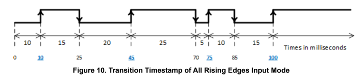
For this example, the FIFO Word Count register will be set to 4 and the FIFO Buffer Data register will contain the following four values (counts of 10 µs):
-
1000 (0x0000 03E8)
-
4500 (0x0000 1194)
-
7500 (0x0000 1D4C)
-
10000 (0x000 2710)
| Time Interval | Calculations | Time between rising edges |
|---|---|---|
| 1 to 2 | 4500 - 1000 = 3500 counts = 3500 * 10 µsec = 35000 µsec = 35.0 msec | 35.0 msec |
| 2 to 3 | 7500 - 4500 = 3000 counts = 3000 * 10 µsec = 30000 µsec = 30.0 msec | 30.0 msec |
| 3 to 4 | 10000 - 7500 = 2500 counts = 2500 * 10 µsec = 25000 µsec = 25.0 msec | 25.0 msec |
Transition Timestamp of All Falling Edges
In this mode, the data in the FIFO buffer is the Falling Edge Timestamp. The timestamp is a 32-bit counter that is incremented at the rate of 100 kHz (in other words, counter is incremented every 10 µsec). The timestamp is can be reset by the application at any time.
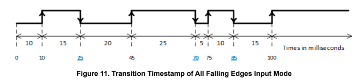
For this example, the FIFO Word Count register will be set to 3 and the FIFO Buffer Data register will contain the following three values (counts of 10 µs):
-
2500 (0x0000 09C4)
-
7000 (0x0000 1B58)
-
8500 (0x0000 2134)
| Time Interval | Calculations | Time between falling edges |
|---|---|---|
| 1 to 2 | 7000 - 2500 = 4500 counts = 4500 * 10 µsec = 45000 µsec = 45.0 msec | 45.0 msec |
| 2 to 3 | 8500 - 7000 = 1500 counts = 1500 * 10 µsec = 15000 µsec = 15.0 msec | 15.0 msec |
Transition Timestamp of All Edges
In this mode, the data in the FIFO buffer is the Rising and Falling Edge Timestamp. The timestamp is a 32-bit counter that is incremented at the rate of 100 kHz (in other words, counter is incremented every 10 µsec). The timestamp is can be reset by the application at any time.
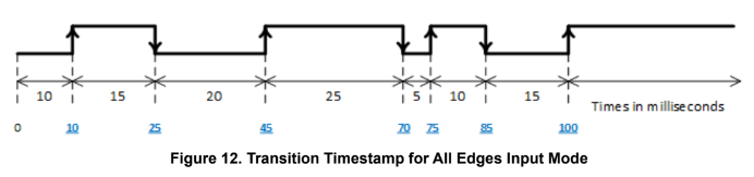
For this example, the FIFO Word Count register will be set to 7 and the FIFO Buffer Data register will contain the following seven values (counts of 10 µs):
- 1000 (0x0000 03E8)
- 2500 (0x0000 09C4)
- 4500 (0x0000 1194)
- 7000 (0x0000 1B58)
- 7500 (0x0000 1D4C)
- 8500 (0x0000 2134)
- 10000 (0x000 2710)
| Time Interval | Calculations | Time between edges |
|---|---|---|
| 1 to 2 | 2500 - 1000 = 1500 counts = 1500 * 10 µsec = 15000 µsec = 15.0 msec | 15.0 msec |
| 2 to 3 | 4500 - 2500 = 2000 counts = 2000 * 10 µsec = 20000 µsec = 20.0 msec | 20.0 msec |
| 3 to 4 | 7000 - 4500 = 2500 counts = 2500 * 10 µsec = 25000 µsec = 25.0 msec | 25.0 msec |
| 4 to 5 | 7500 - 7000 = 500 counts = 500 * 10 µsec = 5000 µsec = 5.0 msec | 5.0 msec |
| 5 to 6 | 8500 - 7500 = 1000 counts = 1000 * 10 µsec = 10000 µsec = 10.0 msec | 10.0 msec |
| 6 to 7 | 10000 - 8500 = 1500 counts = 1500 * 10 µsec = 15000 µsec = 15.0 msec | 15.0 msec |
Transition Counter
There are three Transition Counter features available - Rising Edge Transition Counter, Falling Edge Transition Counter and All Edge Transition Counter.
Rising Edges Transition Counter
In this mode, the count of the number of Rising Edges is recorded. The counter is a 32-bit counter. The counter is can be reset by the application at any time.
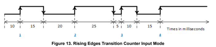
For this example, the Transition Count register will be set to 4.
Falling Edges Transition Counter
In this mode, the count of the number of Falling Edges is recorded. The counter is a 32-bit counter. The counter is can be reset by the application at any time.
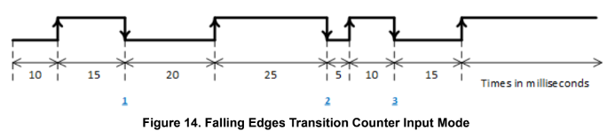
For this example, the Transition Count register will be set to 3.
All Edges Transition Counter
In this mode, the count of the number of Rising and Falling Edges is recorded. The counter is a 32-bit counter. The counter is can be reset by the application at any time.
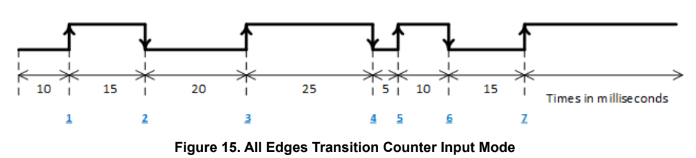
For this example, the Transition Count register will be set to 7.
Period Measurement_
In this input mode, the data in the FIFO buffer is the measurement for each rising edge transition to the next rising edge transition. Timing measurements record the time interval (in 10 µs ticks).
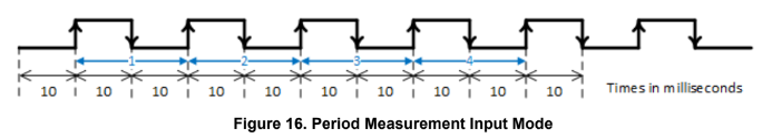
For this example, the FIFO Word Count register will be set to 4 and the FIFO Buffer Data register will contain the following three values (counts of 10 µs):
- 2000 (0x0000 07D0)
- 2000 (0x0000 07D0)
- 2000 (0x0000 07D0)
- 2000 (0x0000 07D0)
| Time Interval | Calculations | Period Measurements |
|---|---|---|
| 1 | 2000 counts * 10 µsec = 20000 µsec = 20.0 msec | 20.0 msec |
| 2 | 2000 counts * 10 µsec = 20000 µsec = 20.0 msec | 20.0 msec |
| 3 | 2000 counts * 10 µsec = 20000 µsec = 20.0 msec | 20.0 msec |
| 4 | 2000 counts * 10 µsec = 20000 µsec = 20.0 msec | 20.0 msec |
Frequency Measurement
In this input mode, the data in the FIFO buffer is the number of rising edge transitions for the programmable time interval programmed in the Frequency Measurement Period register.
For this example, set the Frequency Measurement Period register = 4000 (4000 * 10 µs = 40000 µs = 40 msec).
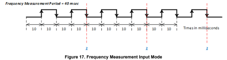
| Time Interval | Calculations | Frequency Measurements |
|---|---|---|
| 1 | 2 counts/40 msec = 2 counts/0.04 seconds = 50 Hz | 50 Hz |
| 2 | 2 counts/40 msec = 2 counts/0.04 seconds = 50 Hz | 50 Hz |
| 3 | 2 counts/40 msec = 2 counts/0.04 seconds = 50 Hz | 50 Hz |
Output Modes
There are three Enhanced Output Functionality modes: two PWM outputs and one Pattern Generator Output mode.
PWM Output
There are two PWM output modes, PWM Continuous and PWM Burst. The PWM timing is very precise with low jitter. In PWM Output mode, the Mode Select register is set to either “PWM Continuous or PWM Burst”. The value written to the PWM Period register specifies the period to output the PWM signal, the value written to the PWM Pulse Width register specifies the time for the “ON” state, and the value written to the PWM Output Polarity register specifies the initial edge of the output. For PWM Burst mode, the PWM Number of Cycles register specifies the number of cycles to output the signal. Note, there may be an initial “OFF” state level delay based on the Period time before the initial pulse is output.
PWM Continuous
Figure 18 and Figure 19 illustrate the PWM Continuous Output signal, one configured with PWM Output Polarity = Positive (0) and one configured with PWM Output Polarity = Negative (1). The configured PWM output is enabled and disabled with the Enable Measurements/Outputs register.
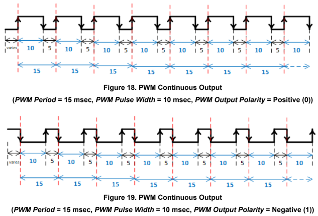
PWM Burst
Figure 20 and Figure 21 illustrate the PWM Burst Output signal with the PWM Number of Cycles = 5 pulses, one configured with PWM Output Polarity = Positive (0) and one configured with PWM Output Polarity = Negative (1). The configured PWM output is enabled with the Enable Measurements/Outputs register. Once the number of pulses that were requested is outputted, the value in the Enable Measurements/Outputs register will be reset (self-clearing) to allow for the output to be re-enabled.
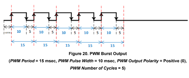
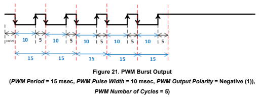
Pattern Generator
For the Pattern Generator mode, there is 64K block of unsigned 32-bit words allocated to specify the data pattern for the output channels. The data in each 32-bit word is bit-mapped per channel. The Pattern RAM Start Address and Pattern RAM End Address registers specify the starting and ending address in the 64K block to use as the data to output for each channel configured for Pattern Generator mode. The Pattern RAM Period register specifies the pattern rate. The Pattern RAM Control and Pattern RAM Number of Cycles control the Pattern Generator output - Continuous, Burst with a specified number of cycles, Pause, or External Trigger from input from Channel 1. Note, when any channel is configured for External Trigger Pattern Generator mode, Channel 1 must be set as an input.
Figure 22 illustrates the output of the 24 channels for the Enhanced Function module all configured in Pattern Generator mode.
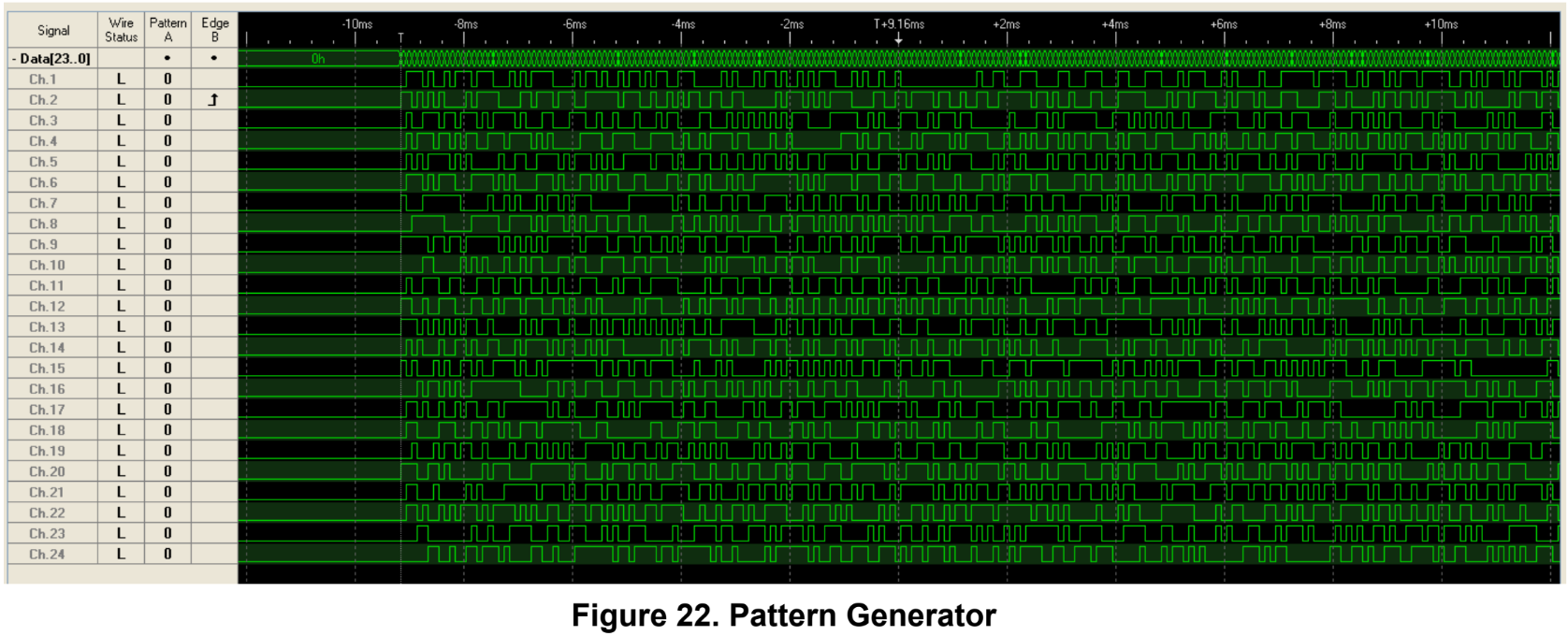
Enhanced Input/Output Functionality Registers
The On-Board Discrete I/O option provides enhanced input and output mode functionality. The Mode Select and Enable Output/Measurement registers are general control registers for the different enhanced input and output modes.
Mode Select
Function: Configures the Enhanced Functionality Modes to apply to the channel.
Type: unsigned binary word (32-bit)
Data Range: See table
Read/Write: R/W
Initialized Value: 0
Operational Settings: It is important that the channel is correctly configured to either input or output in the Input/Output Format registers to correspond to the Enhanced Functionality Mode selected. Setting a 0 to this register will configure that channel to normal operation.
| Mode Select Value (Decimal) | Mode Select Value (Hexadecimal) | Description |
| 0 | 0x0000 0000 | Enhanced Functionality Disabled |
| Input Enhanced Functionality Mode | ||
| 1 | 0x0000 0001 | High Time Pulse Measurements |
| 2 | 0x0000 0002 | Low Time Pulse Measurements |
| 3 | 0x0000 0003 | Transition Timestamp of All Rising Edges |
| 4 | 0x0000 0004 | Transition Timestamp of All Falling Edges |
| 5 | 0x0000 0005 | Transition Timestamp of All Edges |
| 6 | 0x0000 0006 | Rising Edges Transition Counter |
| 7 | 0x0000 0007 | Falling Edges Transition Counter |
| 8 | 0x0000 0008 | All Edges Transition Counter |
| 9 | 0x0000 0009 | Period Measurement |
| 10 | 0x0000 000A | Frequency Measurement |
| Output Enhanced Functionality Mode | ||
| 32 | 0x0000 0020 | PWM Continuous |
| 33 | 0x0000 0021 | PWM Burst |
| 34 | 0x0000 0022 | Pattern Generator |
Enable Measurements/Outputs
Function: Enables/starts the measurements or outputs based on the Mode Select for the channel. Type: unsigned binary word (32-bit)
Data Range: 0x0000 0000 to 0x00FF FFFF
Read/Write: R/W
Initialized Value: 0
Operational Settings: Setting the bit for the associated channel to a 1 will start the measurement or output depending on the Mode Select configuration for that channel. Setting the bit for the associated channel to 0 will stop the measurements/outputs.
Enable Measurements/Outputs
| D31 | D30 | D29 | D28 | D27 | D26 | D25 | D24 | D23 | D22 | D21 | D20 | D19 | D18 | D17 | D16 |
|---|---|---|---|---|---|---|---|---|---|---|---|---|---|---|---|
| 0 | 0 | 0 | 0 | 0 | 0 | 0 | 0 | Ch24 | Ch23 | Ch22 | Ch21 | Ch20 | Ch19 | Ch18 | Ch17 |
| D15 | D14 | D13 | D12 | D11 | D10 | D9 | D8 | D7 | D6 | D5 | D4 | D3 | D2 | D1 | D0 |
| Ch16 | Ch15 | Ch14 | Ch13 | Ch12 | Ch11 | Ch10 | Ch9 | Ch8 | Ch7 | Ch6 | Ch5 | Ch4 | Ch3 | Ch2 | Ch1 |
Input Modes Registers
After configuring the Mode Select register, write a 1 to the Reset Timer/Counter register resets the channel’s timestamp and counter used for input modes. Write a 1 to the Enable Measurements/Outputs register to begin the measurement of the input signal. Write a “0” to the Enable Measurements/Outputs register to stop the measurement of the input signal. The data can be read either while the measurements are being made on input signals or after stopping the measurements.
Reset Timer/Counter
Function: Resets the measurement timestamp and counter for the channel.
Type: unsigned binary word (32-bit)
Data Range: 0x0000 0000 to 0x00FF FFFF
Read/Write: W
Initialized Value: 0
Operational Settings: Setting the bit for the associated channel to a 1 will:
• reset the timestamp used for the Pulse Measurements mode (1-2), Transition Timestamp mode (3-5), and Period Measurement mode (9) and Frequency Measurement mode (10) • reset the counter used for Transition Counter mode (6-8)
Reset Timer/Counter
| D31 | D30 | D29 | D28 | D27 | D26 | D25 | D24 | D23 | D22 | D21 | D20 | D19 | D18 | D17 | D16 |
|---|---|---|---|---|---|---|---|---|---|---|---|---|---|---|---|
| 0 | 0 | 0 | 0 | 0 | 0 | 0 | 0 | Ch24 | Ch23 | Ch22 | Ch21 | Ch20 | Ch19 | Ch18 | Ch17 |
| D15 | D14 | D13 | D12 | D11 | D10 | D9 | D8 | D7 | D6 | D5 | D4 | D3 | D2 | D1 | D0 |
| Ch16 | Ch15 | Ch14 | Ch13 | Ch12 | Ch11 | Ch10 | Ch9 | Ch8 | Ch7 | Ch6 | Ch5 | Ch4 | Ch3 | Ch2 | Ch1 |
FIFO Registers
The FIFO registers are used for the following input modes:
• Pulse Measurements mode (1-2)
• Transition Timestamp mode (3-5)
• Period Measurement mode (9)
• Frequency Measurement mode (10)
FIFO Buffer Data
Function: The data stored in the FIFO Buffer Data is dependent on the input mode.
Type: unsigned binary word (32-bit)
Data Range: 0x0000 0000 to 0xFFFF FFFF
Read/Write: R
Initialized Value: N/A
Operational Settings: Refer to examples in section 2.1.
FIFO Word Count
Function: This is a counter that reports the number of 32-bit words stored in the FIFO buffer.
Type: unsigned binary word (32-bit)
Data Range: 0 - 255 (0x0000 0000 to 0x0000 00FF)
Read/Write: R
Initialized Value: 0
Operational Settings: Every time a read operation is made from the FIFO Buffer Data register, the value in the FIFO Word Count register will be decremented by one. The maximum number of words that can be stored in the FIFO is 255.
FIFO Word Count
| D31 | D30 | D29 | D28 | D27 | D26 | D25 | D24 | D23 | D22 | D21 | D20 | D19 | D18 | D17 | D16 |
|---|---|---|---|---|---|---|---|---|---|---|---|---|---|---|---|
| 0 | 0 | 0 | 0 | 0 | 0 | 0 | 0 | 0 | 0 | 0 | 0 | 0 | 0 | 0 | 0 |
| D15 | D14 | D13 | D12 | D11 | D10 | D9 | D8 | D7 | D6 | D5 | D4 | D3 | D2 | D1 | D0 |
| 0 | 0 | 0 | 0 | 0 | 0 | 0 | 0 | D | D | D | D | D | D | D | D |
Clear FIFO
Function: Clears FIFO by resetting the FIFO Word Count register.
Type: unsigned binary word (32-bit)
Data Range: 0 or 1
Read/Write: W
Initialized Value: N/A
Operational Settings: Write a 1 to resets the Words in FIFO to zero; Clear FIFO register does not clear data in the buffer. A read to the buffer data will give “aged” data.
| D31:D1 | Reserved. Set to 0 |
|---|---|
| D0 | Set to 1 to reset the FIFO Word Count value to zero. |
Clear FIFO
| D31 | D30 | D29 | D28 | D27 | D26 | D25 | D24 | D23 | D22 | D21 | D20 | D19 | D18 | D17 | D16 |
|---|---|---|---|---|---|---|---|---|---|---|---|---|---|---|---|
| 0 | 0 | 0 | 0 | 0 | 0 | 0 | 0 | 0 | 0 | 0 | 0 | 0 | 0 | 0 | 0 |
| D15 | D14 | D13 | D12 | D11 | D10 | D9 | D8 | D7 | D6 | D5 | D4 | D3 | D2 | D1 | D0 |
| 0 | 0 | 0 | 0 | 0 | 0 | 0 | 0 | 0 | 0 | 0 | 0 | 0 | 0 | 0 | D |
FIFO Status
Function: Sets the corresponding bit associated with the FIFO status type; there is a separate register for each channel.
Type: unsigned binary word (32-bit)
Data Range: See table
Read/Write: R
Initialized Value: 0
| Bit | Name | Description |
|---|---|---|
| D31:D4 | Reserved | Set to 0 |
| D3 | Empty | Set to 1 when FIFO Word Count = 0 |
| D2 | Almost Empty | Set to 1 when FIFO Word Count ⇐ 63 (25%) |
| D1 | Almost Full | Set to 1 when FIFO Word Count >= 191 (75%) |
| D0 | Full | Set to 1 when FIFO Word Count = 255 |
FIFO Status
| D31 | D30 | D29 | D28 | D27 | D26 | D25 | D24 | D23 | D22 | D21 | D20 | D19 | D18 | D17 | D16 |
|---|---|---|---|---|---|---|---|---|---|---|---|---|---|---|---|
| 0 | 0 | 0 | 0 | 0 | 0 | 0 | 0 | 0 | 0 | 0 | 0 | 0 | 0 | 0 | 0 |
| D15 | D14 | D13 | D12 | D11 | D10 | D9 | D8 | D7 | D6 | D5 | D4 | D3 | D2 | D1 | D0 |
| 0 | 0 | 0 | 0 | 0 | 0 | 0 | 0 | 0 | 0 | 0 | 0 | D | D | D | D |
_Transition Count Registers*
The Transition Count register are used for the following input modes:
• Transition Counter mode (6-8)
Transition Count
Function: Contains the count of the transitions depending on the configuration in the Mode Select register – Rising Edges, Falling Edges or All Edges.
Type: unsigned binary word (32-bit)
Data Range: 0x0000 0000 to 0xFFFF FFFF
Read/Write: R
Initialized Value: 0
Operational Settings: Refer to examples in Section - Transition Counter.
Frequency Measurement Registers
For the Frequency Measurement mode, the period to perform the frequency measurements must be specified in the Frequency Measurement Period register.
Frequency Measurement Period
Function: When the Mode Select register is programmed for Frequency Measurement mode (10), the value in the Frequency Measurement Period is used as the time interval for counting the number of rising edge transitions within that interval.
Type: unsigned binary word (32-bit)
Data Range: 0x0 to 0xFFFF FFFF
Read/Write: R/W
Initialized Value: 0
Operational Settings: Set the Frequency Measurement Period (LSB = 10 µs). Refer to examples in Section - Frequency Measurement.
Output Modes Registers
After configuring the Mode Select register, write a 1 to the Enable Measurements/Outputs register to outputting the signal. Write a 0 to the Enable Measurements/Outputs register to stop the output signal.
PWM Registers
The PWM Period, PWM Pulse Width and PWM Output Polarity registers configure the PWM output signal. When the Mode Select register is configured for PWM Burst mode, the PWM Number of Cycles register is used to specify the number of cycles to repeat for the burst.
_PWM Period _
Function: When the Mode Select register is programmed for PWM Continuous or PWM Burst mode (32-33), the value in the PWM Period is used as the time interval for outputting the PWM signal.
Type: unsigned binary word (32-bit)
Data Range: 0x0000 0001 to 0xFFFF FFFF
Read/Write: R/W
Initialized Value: 0
Operational Settings: Set the PWM Period (LSB = 10 µs). The PWM Period must be greater than the value set in the PWM Pulse Width register. Refer to examples in Section - PWM Output.
PWM Pulse Width
Function: When the Mode Select register is programmed for PWM Continuous or PWM Burst mode (32-33), the value in the PWM Pulse Width is used as the time interval of the “ON” state for outputting the PWM signal.
Type: unsigned binary word (32-bit)
Data Range: 0x0 to 0xFFFF FFFF
Read/Write: R/W
Initialized Value: 0
Operational Settings: Set the PWM Pulse Width (LSB = 10 µs). The PWM Pulse Width must be less than the value set in the PWM Pulse Width register. Refer to examples in Section - PWM Output.
PWM Output Polarity
Function: When the Mode Select register is programmed for PWM Continuous or PWM Burst mode (32-33), the value in the PWM Output Polarity is used to specify whether the PWM output signal starts with a rising edge (Positive (0)), or a falling edge (Negative (1)).
Type: unsigned binary word (32-bit)
Data Range: 0x0 to 0x00FF FFFF
Read/Write: R/W
Initialized Value: 0
Operational Settings: The PWM Output Polarity register is used to program the starting edge of the PWM Pulse Period (rising or falling). When the PWM output Polarity is set to Positive (0), the output will start with a rising edge, when it’s set to Negative (1), the output will start with a falling edge. The default is Positive (0), which is set when the PWM Polarity bit is 0. Refer to examples in Section - PWM Output.
PWM Output Polarity
| D31 | D30 | D29 | D28 | D27 | D26 | D25 | D24 | D23 | D22 | D21 | D20 | D19 | D18 | D17 | D16 |
|---|---|---|---|---|---|---|---|---|---|---|---|---|---|---|---|
| 0 | 0 | 0 | 0 | 0 | 0 | 0 | 0 | Ch24 | Ch23 | Ch22 | Ch21 | Ch20 | Ch19 | Ch18 | Ch17 |
| D15 | D14 | D13 | D12 | D11 | D10 | D9 | D8 | D7 | D6 | D5 | D4 | D3 | D2 | D1 | D0 |
| Ch16 | Ch15 | Ch14 | Ch13 | Ch12 | Ch11 | Ch10 | Ch9 | Ch8 | Ch7 | Ch6 | Ch5 | Ch4 | Ch3 | Ch2 | Ch1 |
PWM Number of Cycles
Function: When the Mode Select register is programmed for PWM Burst mode (33), the value in the PWM Number of Cycles is used to specify the number of times to repeat the PWM output signal.
Type: unsigned binary word (32-bit)
Data Range: 0x0000 0001 to 0xFFFF FFFF
Read/Write: R/W
Initialized Value: 0
Operational Settings: Set the number of times to output the PWM signal. Refer to examples in Section - PWM Output.
Pattern Generator Registers
The Pattern RAM registers are a 64K block of unsigned 32-bit words allocated to specify the data pattern for the output channels. The Pattern RAM Start Address, Pattern RAM End Address, Pattern RAM Period and Pattern RAM Control registers configure the Pattern Generator output signals. When the Pattern RAM Control register is configured for Burst, the Pattern RAM Number of Cycles specify the number of cycles to repeat the pattern for the burst.
Pattern RAM
Function: Pattern Generator Memory Block from 0x40000 to 0x7FFFC.
Type: unsigned binary word (32-bit)
Address Range: 0x0000 0000 to 0x00FF FFFF
Read/Write: R/W
Initialized Value: 0
Operational Settings: 64K block of unsigned 32-bit words. The data in each 32-bit word is bit-mapped per channel.
Pattern RAM
| D31 | D30 | D29 | D28 | D27 | D26 | D25 | D24 | D23 | D22 | D21 | D20 | D19 | D18 | D17 | D16 |
|---|---|---|---|---|---|---|---|---|---|---|---|---|---|---|---|
| 0 | 0 | 0 | 0 | 0 | 0 | 0 | 0 | Ch24 | Ch23 | Ch22 | Ch21 | Ch20 | Ch19 | Ch18 | Ch17 |
| D15 | D14 | D13 | D12 | D11 | D10 | D9 | D8 | D7 | D6 | D5 | D4 | D3 | D2 | D1 | D0 |
| Ch16 | Ch15 | Ch14 | Ch13 | Ch12 | Ch11 | Ch10 | Ch9 | Ch8 | Ch7 | Ch6 | Ch5 | Ch4 | Ch3 | Ch2 | Ch1 |
Pattern RAM Start Address
Function: When the Mode Select register is programmed for Pattern Generator mode (34), the Pattern RAM Start Address register specifies the starting address within the Pattern RAM block registers to use for the output.
Type: unsigned binary word (32-bit)
Data Range: 0x0004 0000 to 0x0007 FFFC
Read/Write: R/W
Initialized Value: 0
Operational Settings: The value in the Pattern RAM Start Address must be less than the value in the Pattern RAM End Address.
Pattern RAM Start Address
| D31 | D30 | D29 | D28 | D27 | D26 | D25 | D24 | D23 | D22 | D21 | D20 | D19 | D18 | D17 | D16 |
|---|---|---|---|---|---|---|---|---|---|---|---|---|---|---|---|
| 0 | 0 | 0 | 0 | 0 | 0 | 0 | 0 | 0 | 0 | 0 | 0 | 0 | D | D | D |
| D15 | D14 | D13 | D12 | D11 | D10 | D9 | D8 | D7 | D6 | D5 | D4 | D3 | D2 | D1 | D0 |
| D | D | D | D | D | D | D | D | D | D | D | D | D | D | D | D |
Pattern RAM End Address
Function: When the Mode Select register is programmed for Pattern Generator mode (34), the Pattern RAM End Address register specifies the end address within the Pattern RAM block registers to use for the output.
Type: unsigned binary word (32-bit)
Data Range: 0x40000 to 0x7FFFC
Read/Write: R/W
Initialized Value: 0
Operational Settings: The value in the Pattern RAM End Address must be greater than the value in the Pattern RAM Start Address.
Pattern RAM End Address
| D31 | D30 | D29 | D28 | D27 | D26 | D25 | D24 | D23 | D22 | D21 | D20 | D19 | D18 | D17 | D16 |
|---|---|---|---|---|---|---|---|---|---|---|---|---|---|---|---|
| 0 | 0 | 0 | 0 | 0 | 0 | 0 | 0 | 0 | 0 | 0 | 0 | 0 | D | D | D |
| D15 | D14 | D13 | D12 | D11 | D10 | D9 | D8 | D7 | D6 | D5 | D4 | D3 | D2 | D1 | D0 |
| D | D | D | D | D | D | D | D | D | D | D | D | D | D | D | D |
Pattern RAM Period
Function: When the Mode Select register is programmed for Pattern Generator mode (34), the value in the Pattern RAM Period is used as the time interval for outputting the Pattern Generator signals.
Type: unsigned binary word (32-bit)
Data Range: 0x0000 0001 to 0xFFFF FFFF
Read/Write: R/W
Initialized Value: 0
Operational Settings: Set the Pattern RAM Period (LSB = 10 µs).
Pattern RAM Control
Function: When the Mode Select register is programmed for Pattern Generator mode (34), the value in the Pattern RAM Control is used to control the outputting of the Pattern Generator signals.
Type: unsigned binary word (32-bit)
Data Range: See table
Read/Write: R/W
Initialized Value: 0
Operational Settings: Configures the Patter Generator for Continuous, Burst with a specified number of cycles, Pause, or External Trigger from input from Channel 1. Note, when any channel is configured for External Trigger Pattern Generator mode, Channel 1 must be set as an input.
| Bits | Description |
|---|---|
| D31:D5 | Reserved. Set to 0 |
| D4 | Falling Edge External Trigger - Channel 1 used as the input for the trigger |
| D3 | Rising Edge External Trigger - Channel 1 used as the input for the trigger |
| D2 | Pause |
| D1 | Burst Mode - value in Pattern RAM Number of Cycles register defines number of cycles to output |
| D0 | Enable Pattern Generator |
| Values | Description |
|---|---|
| 0x0000 | Disable Pattern Generator, Continuous Mode, No External Trigger |
| 0x0001 | Enable Pattern Generator, Continuous Mode, No External Trigger |
| 0x0002 | Disable Pattern Generator, Burst Mode, No External Trigger |
| 0x0003 | Enable Pattern Generator, Burst Mode, No External Trigger |
| 0x0005 | Enable Pattern Generator, Continuous Mode, Pause, No External Trigger |
| 0x0007 | Enable Pattern Generator, Burst Mode, Pause, No External Trigger |
| 0x0008 | Disable Pattern Generator, Continuous Mode, Rising External Trigger |
| 0x0009 | Enable Pattern Generator, Continuous Mode, Rising External Trigger |
| 0x000A | Disable Pattern Generator, Burst Mode, Rising External Trigger |
| 0x000B | Enable Pattern Generator, Burst Mode, Rising External Trigger |
| 0x000D | Enable Pattern Generator, Continuous Mode, Pause, Rising External Trigger |
| 0x000F | Enable Pattern Generator, Burst Mode, Pause, Rising External Trigger |
| 0x1000 | Disable Pattern Generator, Continuous Mode, Falling External Trigger |
| 0x1001 | Enable Pattern Generator, Continuous Mode, Falling External Trigger |
| 0x1002 | Disable Pattern Generator, Burst Mode, Falling External Trigger |
| 0x1003 | Enable Pattern Generator, Burst Mode, Falling External Trigger |
| 0x1005 | Enable Pattern Generator, Continuous Mode, Pause, Falling External Trigger |
| 0x1007 | Enable Pattern Generator, Burst Mode, Pause, Falling External Trigger |
| 0x0004, 0x0006, 0x000C, 0x000E, 0x1004, 0x1006, 0x1008-0x100F | Invalid |
Pattern RAM Control
| D31 | D30 | D29 | D28 | D27 | D26 | D25 | D24 | D23 | D22 | D21 | D20 | D19 | D18 | D17 | D16 |
|---|---|---|---|---|---|---|---|---|---|---|---|---|---|---|---|
| 0 | 0 | 0 | 0 | 0 | 0 | 0 | 0 | 0 | 0 | 0 | 0 | 0 | 0 | 0 | 0 |
| D15 | D14 | D13 | D12 | D11 | D10 | D9 | D8 | D7 | D6 | D5 | D4 | D3 | D2 | D1 | D0 |
| 0 | 0 | 0 | 0 | 0 | 0 | 0 | 0 | 0 | 0 | 0 | 0 | D | D | D | D |
Pattern RAM Number of Cycles
Function: When the Mode Select register is programmed for Pattern Generator mode (34) and the Pattern RAM Control register is set for Burst mode, the value in the Pattern RAM Number of Cycles is used to specify the number of times to repeat the pattern output signal.
Type: unsigned binary word (32-bit)
Data Range: 0x0000 0001 to 0xFFFF FFFF
Read/Write: R/W
Initialized Value: 0
Operational Settings: Set the number of times to output the pattern.
Enhanced Input/Output Functional Register Map
Key:
Bold Italic = Configuration/Control
Bold Underline = Status
*When an event is detected, the bit associated with the event is set in this register and will remain set until the user clears the event bit. Clearing the bit requires writing a 1 back to the specific bit that was set when read (i.e. write-1-to-clear, writing a ‘1’ to a bit set to ‘1’ will set the bit to ‘0’).
| 0x300C | Mode Select Ch 1 | R/W |
|---|---|---|
| 0x308C | Mode Select Ch 2 | R/W |
| 0x310C | Mode Select Ch 3 | R/W |
| 0x318C | Mode Select Ch 4 | R/W |
| 0x320C | Mode Select Ch 5 | R/W |
| 0x328C | Mode Select Ch 6 | R/W |
| 0x330C | Mode Select Ch 7 | R/W |
| 0x338C | Mode Select Ch 8 | R/W |
| 0x340C | Mode Select Ch 9 | R/W |
| 0x348C | Mode Select Ch 10 | R/W |
| 0x350C | Mode Select Ch 11 | R/W |
| 0x358C | Mode Select Ch 12 | R/W |
| 0x360C | Mode Select Ch 13 | R/W |
| 0x368C | Mode Select Ch 14 | R/W |
| 0x370C | Mode Select Ch 15 | R/W |
| 0x378C | Mode Select Ch 16 | R/W |
| 0x380C | Mode Select Ch 17 | R/W |
| 0x388C | Mode Select Ch 18 | R/W |
| 0x390C | Mode Select Ch 19 | R/W |
| 0x398C | Mode Select Ch 20 | R/W |
| 0x3A0C | Mode Select Ch 21 | R/W |
| 0x3A8C | Mode Select Ch 22 | R/W |
| 0x3B0C | Mode Select Ch 23 | R/W |
| 0x3B8C | Mode Select Ch 24 | R/W |
| 0x2000 | Enable Measurements/Outputs | R/W |
|---|
Input Modes Registers
| 0x2004 | Reset Timer/Counter | W |
|---|
FIFO Registers
| 0x3000 | FIFO Buffer Data Ch 1 | R |
|---|---|---|
| 0x3080 | FIFO Buffer Data Ch 2 | R |
| 0x3100 | FIFO Buffer Data Ch 3 | R |
| 0x3180 | FIFO Buffer Data Ch 4 | R |
| 0x3200 | FIFO Buffer Data Ch 5 | R |
| 0x3280 | FIFO Buffer Data Ch 6 | R |
| 0x3300 | FIFO Buffer Data Ch 7 | R |
| 0x3380 | FIFO Buffer Data Ch 8 | R |
| 0x3400 | FIFO Buffer Data Ch 9 | R |
| 0x3480 | FIFO Buffer Data Ch 10 | R |
| 0x3500 | FIFO Buffer Data Ch 11 | R |
| 0x3580 | FIFO Buffer Data Ch 12 | R |
| 0x3600 | FIFO Buffer Data Ch 13 | R |
| 0x3680 | FIFO Buffer Data Ch 14 | R |
| 0x3700 | FIFO Buffer Data Ch 15 | R |
| 0x3780 | FIFO Buffer Data Ch 16 | R |
| 0x3800 | FIFO Buffer Data Ch 17 | R |
| 0x3880 | FIFO Buffer Data Ch 18 | R |
| 0x3900 | FIFO Buffer Data Ch 19 | R |
| 0x3980 | FIFO Buffer Data Ch 20 | R |
| 0x3A00 | FIFO Buffer Data Ch 21 | R |
| 0x3A80 | FIFO Buffer Data Ch 22 | R |
| 0x3B00 | FIFO Buffer Data Ch 23 | R |
| 0x3B80 | FIFO Buffer Data Ch 24 | R |
| 0x3004 | FIFO Word Count Ch 1 | R |
|---|---|---|
| 0x3084 | FIFO Word Count Ch 2 | R |
| 0x3104 | FIFO Word Count Ch 3 | R |
| 0x3184 | FIFO Word Count Ch 4 | R |
| 0x3204 | FIFO Word Count Ch 5 | R |
| 0x3284 | FIFO Word Count Ch 6 | R |
| 0x3304 | FIFO Word Count Ch 7 | R |
| 0x3384 | FIFO Word Count Ch 8 | R |
| 0x3404 | FIFO Word Count Ch 9 | R |
| 0x3484 | FIFO Word Count Ch 10 | R |
| 0x3504 | FIFO Word Count Ch 11 | R |
| 0x3584 | FIFO Word Count Ch 12 | R |
| 0x3604 | FIFO Word Count Ch 13 | R |
| 0x3684 | FIFO Word Count Ch 14 | R |
| 0x3704 | FIFO Word Count Ch 15 | R |
| 0x3784 | FIFO Word Count Ch 16 | R |
| 0x3804 | FIFO Word Count Ch 17 | R |
| 0x3884 | FIFO Word Count Ch 18 | R |
| 0x3904 | FIFO Word Count Ch 19 | R |
| 0x3984 | FIFO Word Count Ch 20 | R |
| 0x3A04 | FIFO Word Count Ch 21 | R |
| 0x3A84 | FIFO Word Count Ch 22 | R |
| 0x3B04 | FIFO Word Count Ch 23 | R |
| 0x3B84 | FIFO Word Count Ch 24 | R |
| 0x3008 | FIFO Status Ch 1 | R |
|---|---|---|
| 0x3088 | FIFO Status Ch 2 | R |
| 0x3108 | FIFO Status Ch 3 | R |
| 0x3188 | FIFO Status Ch 4 | R |
| 0x3208 | FIFO Status Ch 5 | R |
| 0x3288 | FIFO Status Ch 6 | R |
| 0x3308 | FIFO Status Ch 7 | R |
| 0x3388 | FIFO Status Ch 8 | R |
| 0x3408 | FIFO Status Ch 9 | R |
| 0x3488 | FIFO Status Ch 10 | R |
| 0x3508 | FIFO Status Ch 11 | R |
| 0x3588 | FIFO Status Ch 12 | R |
| 0x3608 | FIFO Status Ch 13 | R |
| 0x3688 | FIFO Status Ch 14 | R |
| 0x3708 | FIFO Status Ch 15 | R |
| 0x3788 | FIFO Status Ch 16 | R |
| 0x3808 | FIFO Status Ch 17 | R |
| 0x3888 | FIFO Status Ch 18 | R |
| 0x3908 | FIFO Status Ch 19 | R |
| 0x3988 | FIFO Status Ch 20 | R |
| 0x3A08 | FIFO Status Ch 21 | R |
| 0x3A88 | FIFO Status Ch 22 | R |
| 0x3B08 | FIFO Status Ch 23 | R |
| 0x3B88 | FIFO Status Ch 24 | R |
| 0x2008 | Reset FIFO | W |
|---|
Transition Count Registers
| 0x3000 | Transition Count Ch 1 | R |
|---|---|---|
| 0x3080 | Transition Count Ch 2 | R |
| 0x3100 | Transition Count Ch 3 | R |
| 0x3180 | Transition Count Ch 4 | R |
| 0x3200 | Transition Count Ch 5 | R |
| 0x3280 | Transition Count Ch 6 | R |
| 0x3300 | Transition Count Ch 7 | R |
| 0x3380 | Transition Count Ch 8 | R |
| 0x3400 | Transition Count Ch 9 | R |
| 0x3480 | Transition Count Ch 10 | R |
| 0x3500 | Transition Count Ch 11 | R |
| 0x3580 | Transition Count Ch 12 | R |
| 0x3600 | Transition Count Ch 13 | R |
| 0x3680 | Transition Count Ch 14 | R |
| 0x3700 | Transition Count Ch 15 | R |
| 0x3780 | Transition Count Ch 16 | R |
| 0x3800 | Transition Count Ch 17 | R |
| 0x3880 | Transition Count Ch 18 | R |
| 0x3900 | Transition Count Ch 19 | R |
| 0x3980 | Transition Count Ch 20 | R |
| 0x3A00 | Transition Count Ch 21 | R |
| 0x3A80 | Transition Count Ch 22 | R |
| 0x3B00 | Transition Count Ch 23 | R |
| 0x3B80 | Transition Count Ch 24 | R |
Frequency Measurement Registers
| 0x3014 | Frequency Measurement Period Ch 1 | R/W |
|---|---|---|
| 0x3094 | Frequency Measurement Period Ch 2 | R/W |
| 0x3114 | Frequency Measurement Period Ch 3 | R/W |
| 0x3194 | Frequency Measurement Period Ch 4 | R/W |
| 0x3214 | Frequency Measurement Period Ch 5 | R/W |
| 0x3294 | Frequency Measurement Period Ch 6 | R/W |
| 0x3314 | Frequency Measurement Period Ch 7 | R/W |
| 0x3394 | Frequency Measurement Period Ch 8 | R/W |
| 0x3414 | Frequency Measurement Period Ch 9 | R/W |
| 0x3494 | Frequency Measurement Period Ch 10 | R/W |
| 0x3514 | Frequency Measurement Period Ch 11 | R/W |
| 0x3594 | Frequency Measurement Period Ch 12 | R/W |
| 0x3614 | Frequency Measurement Period Ch 13 | R/W |
| 0x3694 | Frequency Measurement Period Ch 14 | R/W |
| 0x3714 | Frequency Measurement Period Ch 15 | R/W |
| 0x3794 | Frequency Measurement Period Ch 16 | R/W |
| 0x3814 | Frequency Measurement Period Ch 17 | R/W |
| 0x3894 | Frequency Measurement Period Ch 18 | R/W |
| 0x3914 | Frequency Measurement Period Ch 19 | R/W |
| 0x3994 | Frequency Measurement Period Ch 20 | R/W |
| 0x3A14 | Frequency Measurement Period Ch 21 | R/W |
| 0x3A94 | Frequency Measurement Period Ch 22 | R/W |
| 0x3B14 | Frequency Measurement Period Ch 23 | R/W |
| 0x3B94 | Frequency Measurement Period Ch 24 | R/W |
Output Mode Registers
PWM Registers
| 0x3014 | PWM Period Ch 1 | R/W |
|---|---|---|
| 0x3094 | PWM Period Ch 2 | R/W |
| 0x3114 | PWM Period Ch 3 | R/W |
| 0x3194 | PWM Period Ch 4 | R/W |
| 0x3214 | PWM Period Ch 5 | R/W |
| 0x3294 | PWM Period Ch 6 | R/W |
| 0x3314 | PWM Period Ch 7 | R/W |
| 0x3394 | PWM Period Ch 8 | R/W |
| 0x3414 | PWM Period Ch 9 | R/W |
| 0x3494 | PWM Period Ch 10 | R/W |
| 0x3514 | PWM Period Ch 11 | R/W |
| 0x3594 | PWM Period Ch 12 | R/W |
| 0x3614 | PWM Period Ch 13 | R/W |
| 0x3694 | PWM Period Ch 14 | R/W |
| 0x3714 | PWM Period Ch 15 | R/W |
| 0x3794 | PWM Period Ch 16 | R/W |
| 0x3814 | PWM Period Ch 17 | R/W |
| 0x3894 | PWM Period Ch 18 | R/W |
| 0x3914 | PWM Period Ch 19 | R/W |
| 0x3994 | PWM Period Ch 20 | R/W |
| 0x3A14 | PWM Period Ch 21 | R/W |
| 0x3A94 | PWM Period Ch 22 | R/W |
| 0x3B14 | PWM Period Ch 23 | R/W |
| 0x3B94 | PWM Period Ch 24 | R/W |
| 0x3010 | PWM Pulse Width Ch 1 | R/W |
|---|---|---|
| 0x3090 | PWM Pulse Width Ch 2 | R/W |
| 0x3110 | PWM Pulse Width Ch 3 | R/W |
| 0x3190 | PWM Pulse Width Ch 4 | R/W |
| 0x3210 | PWM Pulse Width Ch 5 | R/W |
| 0x3290 | PWM Pulse Width Ch 6 | R/W |
| 0x3310 | PWM Pulse Width Ch 7 | R/W |
| 0x3390 | PWM Pulse Width Ch 8 | R/W |
| 0x3410 | PWM Pulse Width Ch 9 | R/W |
| 0x3490 | PWM Pulse Width Ch 10 | R/W |
| 0x3510 | PWM Pulse Width Ch 11 | R/W |
| 0x3590 | PWM Pulse Width Ch 12 | R/W |
| 0x3610 | PWM Pulse Width Ch 13 | R/W |
| 0x3690 | PWM Pulse Width Ch 14 | R/W |
| 0x3710 | PWM Pulse Width Ch 15 | R/W |
| 0x3790 | PWM Pulse Width Ch 16 | R/W |
| 0x3810 | PWM Pulse Width Ch 17 | R/W |
| 0x3890 | PWM Pulse Width Ch 18 | R/W |
| 0x3910 | PWM Pulse Width Ch 19 | R/W |
| 0x3990 | PWM Pulse Width Ch 20 | R/W |
| 0x3A10 | PWM Pulse Width Ch 21 | R/W |
| 0x3A90 | PWM Pulse Width Ch 22 | R/W |
| 0x3B10 | PWM Pulse Width Ch 23 | R/W |
| 0x3B90 | PWM Pulse Width Ch 24 | R/W |
| 0x3018 | PWM Number of Cycles Ch 1 | R/W |
|---|---|---|
| 0x3098 | PWM Number of Cycles Ch 2 | R/W |
| 0x3118 | PWM Number of Cycles Ch 3 | R/W |
| 0x3198 | PWM Number of Cycles Ch 4 | R/W |
| 0x3218 | PWM Number of Cycles Ch 5 | R/W |
| 0x3298 | PWM Number of Cycles Ch 6 | R/W |
| 0x3318 | PWM Number of Cycles Ch 7 | R/W |
| 0x3398 | PWM Number of Cycles Ch 8 | R/W |
| 0x3418 | PWM Number of Cycles Ch 9 | R/W |
| 0x3498 | PWM Number of Cycles Ch 10 | R/W |
| 0x3518 | PWM Number of Cycles Ch 11 | R/W |
| 0x3598 | PWM Number of Cycles Ch 12 | R/W |
| 0x3618 | PWM Number of Cycles Ch 13 | R/W |
| 0x3698 | PWM Number of Cycles Ch 14 | R/W |
| 0x3718 | PWM Number of Cycles Ch 15 | R/W |
| 0x3798 | PWM Number of Cycles Ch 16 | R/W |
| 0x3818 | PWM Number of Cycles Ch 17 | R/W |
| 0x3898 | PWM Number of Cycles Ch 18 | R/W |
| 0x3918 | PWM Number of Cycles Ch 19 | R/W |
| 0x3998 | PWM Number of Cycles Ch 20 | R/W |
| 0x3A18 | PWM Number of Cycles Ch 21 | R/W |
| 0x3A98 | PWM Number of Cycles Ch 22 | R/W |
| 0x3B18 | PWM Number of Cycles Ch 23 | R/W |
| 0x3B98 | PWM Number of Cycles Ch 24 | R/W |
| 0x200C | PWM Output Polarity | R/W |
|---|
Pattern Generator Registers
| 0x0004 0000 to 0x0007 FFFC |
|---|
| Pattern RAM |
| R/W |
| 0x2010 | Pattern RAM Period | R/W |
|---|---|---|
| 0x2014 | Pattern RAM Start Address | R/W |
| 0x2018 | Pattern RAM End Address | R/W |
| 0x201C | Pattern RAM Control | R/W |
| 0x2020 | Pattern RAM Number of Cycles | R/W |
Revision History
Motherboard Manual - 67G6 Revision History
| Revision | Revision Date | Description |
|---|---|---|
| C | 2022-02-01 | ECO C09043, transition to docbuilder format. Pg.7, updated from ‘Over 70 different functions’ to ‘Over 100 different modules’. Pg.7, updated product image. Pg.7, updated general description. Pg.8-9, updated available module functions table. Pg.10, added ‘+3.3_AUX’ power spec to ‘General Specifications’. |
| C1 | 2022-04-19 | ECO C09237, Pg.47-51, revised P0/P1/P2-P6 pinout tables to meet VPX standard format. Pg.63, corrected option numbering in ‘Notes’ table. Pg.64, changed DSE/DRE/DLE Power/CH maximum (VA) value from ‘1.5’ to ‘2.2’. |
| C2 | 2023-03-10 | ECO C09299, pg.48, revised P1 pinout table rows 1 & 2 to clarify PCIe lanes 1 & 2. Pg.48, removed ‘0’ from PCIe callouts in P1 pinout table rows 1-4. Pg.64, added Single Channel note. |
| C3 | 2023-03-28 | ECO C10228, pg.7, updated product description. Pg.8, moved VR1 to ‘I/O Modules’. Pg.9, replaced SC2/SC7 with SC5/SC6 in ‘Communication Modules’. Pg.10, updated Introduction; added 67G6 Overview. Pg.11, updated 5VDC power to 2.2 A. Pg.16, added Module Slot Addressing<br>Ready. Pg.36, added Module Slot Addressing Ready offset. Pg.47, changed pin D5 from N/C to ()3.3V. Pgs.73/76/79, updated D12-D10 in register table to ‘D’ to accommodate full Integer Mode range. Pgs.73-76/79, changed VRMS to VDC. Pg.74, updated Upper Threshold operations settings to ‘…below the Upper…‘. Pg.74, updated Lower Threshold operations settings to ‘…above the Lower…‘. Pg.78, added ‘mA’ to ‘5’ in Function. Pg.83-87, removed ‘pendings’ from status registers. Pg.83, corrected # of channels for data range/initialized value in “Channel StatusEnabled”. Pg.84, added 2nd note to Voltage Reading and Driver Error. Pg.84, updated Driver Error function. Pg.85, changed Low-to-High/High-to-Low Transition Status function to ‘event’. Pg.85, added 3rd note to Low-to-High/High-to-Low Transition status. Pg.86, changed Above Max High Threshold Status function to ‘event’. Pg.87, changed Below Min Low Threshold Status function to ‘event’. Pg.87, changed Mid-Range Status to ‘event’; added notes to Mid-Range Status. |
| C4 | 2023-10-31 | ECO C10902, pg.49, corrected Module 5 and Module 6 color code reference table (Module 6 I/O now Module 5 I/O; Module 5 I/O now Module 6 I/O). Pg.78, changed ‘…two VCC banks’ to ‘four VCC banks’. Pg.78, added voltage sensing details to initialized value & operations settings. Pg.85, changed ‘High-to-Low’ to ‘Low-to-High’ in register description. Pg.87, changed ‘Above Max High’ to ‘Below Min Low’ in register description. |
| C5 | 2024-05-01 | ECO C11486, pg.7, updated product image. Pg.7, added DLx/DSx(DRx)/SDx modules to available modules table. Pg.8, added CMF module to available modules table. Pg.66, updated register names in Input section. Pg.66, updated I/O circuits figure to remove diode from LS/HS drive output configs & ‘open collect’ from LS drive output config. Pg.67, added Voltage to threshold level names; updated threshold diagram. Pg.68, changed Threshold to Voltage in Above Max High/Below Min Low/Mid-Range. Pg.68, revised register names in Unit Conversions. Pg.68, updated Note. Pg.70, changed Input/Output Format Low to I/O Format Ch1-16. Pg.70, changed Input/Output Format High to I/O Format Ch17-24. Pg.72, added Voltage to section heading and threshold level names in bit table. Pg.72, changed Max High Threshold to Max High Voltage Threshold. Pg.73, changed Upper Threshold to Upper Voltage Threshold. Pg.73, changed Lower Threshold to Lower Voltage Threshold. Pg.74, changed Min Low Threshold to Min Low Voltage Threshold. Pg.77, changed Select Pullup or Pulldown to Select Pull-Up or Pull-Down. Pg.77, changed VCC Bank Reading to VCC Voltage Reading. Pg.77, changed Current for Source/Sink to Pull-Up/Down Current. Pg.78, changed VCC Bank Reading to VCC Voltage Reading. Pg.81, changed Reset BIT to BIT Count Clear. Pg.82, changed Channel Status Enabled to Channel Status Enable. Pg.85, changed Above Max High Threshold to Above Max High Voltage. Pg.86, changed Below Min Low Threshold to Below Min Low Voltage. Pg.86, changed Mid-Range to MidRange Voltage. Pg.88-92, updated register offset names per revised register description names. Pg.93-94, added list of revised register description names. |
NAI Cares
North Atlantic Industries (NAI) is a leading independent supplier of Embedded I/O Boards, Single Board Computers, Rugged Power Supplies, Embedded Systems and Motion Simulation and Measurement Instruments for the Military, Aerospace and Industrial Industries. We accelerate our clients’ time-to-mission with a unique approach based on a Configurable Open Systems Architecture™ (COSA®) that delivers the best of both worlds: custom solutions from standard COTS components.
We have built a reputation by listening to our customers, understanding their needs, and designing, testing and delivering board and system-level products for their most demanding air, land and sea requirements. If you have any applications or questions regarding the use of our products, please contact us for an expedient solution.
Please visit us at: www.naii.com or select one of the following for immediate assistance:
Documentation
FAQ
Application Notes
http://www.naii.com/applicationnotes
Calibration and Repairs
http://www.naii.com/calibrationrepairs
Call Us
(631) 567-1100
Link to original