
INTRODUCTION
Precision Time Protocol (PTP)
This board supports PTP (IEEE 1588) time synchronization over its Ethernet ports. See the PTP guide for the included software package, supported PetaLinux images, and how to use it.
This manual provides information about the North Atlantic Industries, Inc. (NAI) NIU3A System. The NIU3A is a “Nano Interface Unit”; self-contained Multifunction I/O System preconfigured with 24-CH programmable Discrete I/O, 8-CH ARINC 429/575, 4-CH CANBus and 2-CH MIL-STD-1553 functions. The NIU3A can also be configured with up to three additional smart Configurable Open Systems Architecture™ (COSA®) function modules. The NIU3A boasts a dual ARM ®Cortex®-A53 processor for customer application and I/O and communications management.
For a brief description of the system and complete list of features, click here for the NIU3A data sheet.
SOFTWARE SUPPORT
The ENAIBL Software Support Kit (SSK) is supplied with all system platform based board level products. This platform’s SSK contents include html format help documentation which defines board specific library functions and their respective parameter requirements. A board specific library and its source code is provided (module level ‘C’ and header files) to facilitate function implementation independent of user operating system (O/S). Portability files are provided to identify Board Support Package (BSP) dependent functions and help port code to other common system BSPs. With the use of the provided help documentation, these libraries are easily ported to any 32-bit O/S such as RTOS or Linux.
The latest version of a board specific SSK can be downloaded from our website www.naii.com in the software downloads section. Software setup is covered in Choosing the Right SSK and the SSK package guides (SSK 1.x, SSK 2.x); packages are on the Downloads page. For other operating system support, contact factory.
CONVENTIONS USED IN THIS MANUAL

Note
An operating procedure, practice, or condition, etc., that is essential to emphasize.
All numbers are expressed in decimal format unless otherwise noted.
Website
GENERAL SAFETY NOTICES
The following general safety notices supplement the specific warnings and cautions appearing elsewhere in the manual. They are recommended precautions that must be understood and applied during operation and maintenance of the instrument covered herein.
Death or serious injury may result if personnel fail to observe safety precautions. Dependent on configuration, some modules (e.g. Synchro / Resolver or AC signal sources) can generate output signals with high voltages. Be careful not to contact high-voltage connections when installing, operating or maintaining this instrument.

The NIU3A is delivered as a standalone system with no accessible or serviceable parts.
Repair
DO NOT ATTEMPT REPAIR. Under no circumstances should repair of this instrument be attempted. All repairs to this chassis must be accomplished at the factory.
High Voltage

HIGH VOLTAGE may be used in the operation of this equipment.
Input Power Always On

Note
The design of the model NIU3A is such that DC input power is continuously supplied to internal circuits when connected to a main power source. To disconnect the NIU3A from external power, the external power source should first be de-energized. The power input cable can then be disconnected.
SYSTEM SPECIFICATIONS & DETAILS
Introduction
The Nano Interface Unit (NIU3A) is a second-generation, integrated, compact, “nano-sized” subsystem with unprecedented I/O capability configurations. The NIU3A connects to existing platform Ethernet networks, making data available to any system on the network. Additionally, the NIU3A is delivered with ARM® Cortex®-A53 access support for standalone or other processor related capability. The NIU3A easily adds sensor data acquisition and distribution and communication interfaces to mission computers without expensive chassis and backplane redesign. It has been designed with rugged embedded industrial, military and aerospace applications in mind. Leveraging NAI’s field-proven, unique modular architecture, the NIU3A supports a wide selection of different Intelligent I/O, motion simulation/measurement and communications functions such as:
| A/D Converter | D/A Converter | I/O TTL/CMOS | RTD | I/O Discrete |
| I/O Differential Transceiver | Synchro/Resolver LVDT/RVDT Measurement | Synchro/Resolver LVDT/RVDT Simulation | Strain Gage | Encoder |
| Dual-Channel Dual Redundant BC/RT/MT MIL-STD-1553 | High-Speed Sync/Async RS232/422/423/485 | ARINC 429/575 | CANBus | I/O Relay |
| AC Reference | Ethernet Switch | SSD/Flash |
This approach provides unprecedented flexibility for supporting existing or new applications where there are specific interfacing requirements.
Significant application benefits include:
-
Independent (pre-processed) I/O functionality targeted to specific data acquisition/control areas
-
Additional capabilities, technology insertion and sensor interfacing to existing fielded applications
-
Minimal integration risk based on current field-proven, deployed technologies
-
Only ~ 7.2” x 5.5” x 3.2” @ ~5.4 lbs. (2.45 kg) conduction/convection cooled
-
2x Ethernet
- 10/100/1000Base-T (GbE) (default)
Objectives
This manual provides the user with basic hardware implementation and information regarding the operation and interface of the NIU3A. Each NIU3A is fitted with one, two or three function modules, four embedded module functions, dual-core processor and an integrated motherboard, power supply unit (PSU) and interface connectors.
Scope
This manual covers the basic operation of the NIU3A as a standalone I/O subsystem with pertinent/specific details relating to the operation/communications from/to the NIU3A with the available function module(s) fitted within the NIU3A.
ON BOARD RESOURCES
Memory
DDR4 SDRAM
The NIU3A provides a total of 8 GB of ECC DDR4 memory. This memory is organized as 4 1Gb x 16 MT40A1G16RC devices (parts may vary), with a fifth device providing storage for ECC data. The Ultrascale+™ has an on chip 64-bit DDR4 memory controller. The controller has full ECC error-correction support, with the ability to detect multi-bit errors and correct single-bit errors within a nibble. Please consult the Micron data sheet for DDR4 device specific details.
NOR Flash
Connected through the local bus, the NIU3A supports 2 x 2 gigabytes of flash. The Flash consists of a stacked (four 512Mb die) Micron® Flash MT25QL02GCBB8E12-0SIT device. Flash features a high-speed SPI-compatible bus interface that utilizes dual QSPI via a two-input logic gate to increase I/O throughput rates four times for each device. The NOR Flash has an erase capacity of 100,000 cycles per sector and typical data retention of 20 years.
FRAM
The FM24CL64B is a 64-kilobit nonvolatile memory employing an advanced ferroelectric process. The ferroelectric random-access memory or FRAM is nonvolatile and performs reads and writes like a RAM. It provides reliable data retention for 38 years. The NIU3A FRAM 64K bits are organized as 8,192 x 8 bits random access memory, connected to the Ultrascale+™ CPU through the I2C controller.
SATA
The Ultrascale+™ CPU is directly connected to an onboard Solid-State Drive (SSD). The SSD contains a single level cell NAND Flash together with a controller in a single Multi-Chip package. The Multi-Chip packaged device is soldered directly to the printed circuit board for reliable electrical and mechanical connection.
The SSD has an internal write protect signal SATA_WP. The SATA_WP signal must be connected or switched to ground to enable any write to the SSD. The SATA_WP signal is pulled up on card by a 4.7 KΩ resistor to the internal 3.3 V supply.
The onboard SATA drive conforms to the follow specifications:
- Complies with Serial ATA 2.5 Specification
- Supports speeds: 1.5 Gbps (first-generation SATA), 3 Gbps (second-generation SATA and eSATA)
- Supports advanced technology attachment packet interface (ATAPI) devices
- Contains high-speed descriptor-based DMA controller
- Supports native command queuing (NCQ) commands
The standard ordering code for the NIU3A includes a 32GB SSD drive. Larger devices are available; please consult the factory for availability.
Peripheral I/O
Ethernet
The NIU3A supports two 10/100/1000Base-TX Ethernet connections using two Marvell Alaska 88E1512 Ethernet PHY devices and the Xilinx Gigabit Ethernet MACs. The PHY-to-MAC interface employs a Reduced Gigabit Media Independent Interface (RGIII) connection using four data lines at 250 Mbps each for a connection speed of 1 Gbps. The NIU3A contains internal magnetics and can directly drive copper CAT5e or CAT6 twisted pairs.
The NIU3A Ethernet ports support:
- Detection and correction of pair swaps (MDI crossover), and pair polarity
- MAC-side and line-side loopback
- Auto-negotiation
Ethernet Port 1 can be routed as 10/100/1000Base-TX Ethernet as a build option.
Ethernet Port 2 can be routed as 10/100/1000Base-TX Ethernet as a build option.
I/O pin outs can be found in the Pinout Details section of this document.
USB
The NIU3A supports one USB 2.0 port. Contact factory for availability.
USB0 is available on the NIU3A, on connector J2. The USB port can operate as a standalone host.
- Compatible with USB specification, Rev. 2.0
- Supports high-speed (480 Mbps), full-speed (12 Mbps), and low-speed (1.5 Mbps) operations
- Supports operation as a standalone USB host controller
- Supports USB root hub with one downstream-facing port
- Enhanced host controller interface (EHCI)-compatible
- One controller supports operation as a standalone USB device
- Supports one upstream-facing port
- Supports six programmable USB endpoints
I2C
I2C is a two-wire, bidirectional single ended serial bus that provides an efficient method of exchanging data between a master and slave device. The NIU3A has one I2C device for communicating with onboard devices, as shown in the table below.
| Assignment | I2C addresses | Device |
| Onboard Devices | 0x50 | Security Manager |
| Onboard Devices | 0x56 | EEPROM |
| Onboard Devices | 0x53 | FRAM |
Serial Port
The NIU3A has a single, asynchronous serial port. The interface uses a two-wire, TXD, RXD interface (system/power GND referenced). The SER-TXD and SER-RXD RS-232 signals are routed to J2 on the NIU3A.
Tamper Detect Interface and Action Circuit
NAI is developing an optional Tamper Detect Interface and Action Circuit for improved Security/Cybersecurity requirements. This circuit will offer FIPS 140-3 Level 3 Design Support, Crypto-Key Storage (with Battery-Backed RAM), Secure Boot and Anti-Tamper/Tamper Detect & Sanitize functions. For further information, please contact NAI.
Software Libraries/Associated Documents
NIU3A BSP Processor Module Library
The NIU3A Processor library package provides function interfaces to the on-module functionality. This package contains Help documentation (in html format) that explains all the functions available in the library. The package also contains the source code (**.h, **.c) files as well as the files needed to build the library using any of the supported operating systems. Example programs are also provided to demonstrate the usage of the libraries in typical applications of the module.
Associated Documents
Check the NAI website or contact factory for the latest downloads and documentation.
SPECIFICATIONS
The NIU3A is designed to meet the following general specifications.
General
| Ethernet Data Transfer: | Data transfers within 1 ms (typical) |
| Input Voltage: | 18 to 36 VDC (28 VDC nominal) |
| Power (Base unit): | 0.571 A (~16 W) @ 28 V VDC nominal plus module(s) power (see specific module(s) specifications) I/O Signal GND reference is isolated from main power source return and chassis. |
| Power/Heat Dissipation: | ~30 watts (maximum) when properly mounted to a cold-plate, which must be maintained at a temperature not to exceed 71°C. Note: The total NIU3A power dissipation is dependent on the configuration of the modules fitted in the NIU3A. |
| Temperature, Operating: | -40°C to 71°C (conduction cooled - measured at cold plate interface) |
| Temperature, Storage: | -55°C to 105°C |
| Size: | Height: ~3.2" (81.3 mm) Depth: ~5.5" (139.7 mm) Width: ~7.2” (182.9 mm) |
| Weight: | The weight of an NIU3A system is dependent on the configuration. The approximate weight of the NIU3U is based on the selection of the functional module. The approximate weight of a typical fully configured NIU3A (model #) is ~5.4 lbs. (2.45 kg). |
Environmental
| Environmental MIL-STD-810 (*1) | ||||||
| No. | Description | Procedure | Cycles | Table | Figure | Comments |
| 514 | Random Vibe | Method 514.6, 0.1g2/Hz from 100 to 1K Hz., -3dB octave 5-100 Hz and -6dB 1K-2K Hz,(Operational) | ||||
| 514 | Sinusoidal Vibe | TBD | ||||
| 501 | Temp (High) | 3 | 3 periods (@ 4 hrs. ea.) within 24 hrs. cycle at 71 ºC baseplate | |||
| 502 | Temp (Low) | 1 | 3 periods (@ 4 hrs. ea.) within 24 hrs. cycle at -40 ºC baseplate | |||
| 503 | Temp (Shock) | 3 | 3 x 1 hr. each hot & cold cycles (non-operational) | |||
| 507 | Humidity | II | 10 | 507.5-7 | 507.5-IX | Cyclic high humidity (Cycle B2) |
| 500 | Altitude (50K) | II | 1 | n/a | n/a | 10m/s to 50,000ft for 1 hr. |
| 500 | Altitude (70K) | II | 1 | n/a | n/a | 10m/s to 70,000ft for 1 hr. |
| 513 | Acceleration | II | 1 | 513.6-II | n/a | Carrier-based Aircraft (18g's max) |
| 516 | Shock - Operating | I | 3 | 516.6-I | n/a | 40g's, 3 pulses each ± X, Y, Z axis (total of 18 shock pulses) |
| 516 | Shock - Crash | V | 3 | 516.6-I | n/a | 75g's, 3 pulses each ± X, Y, Z axis (total of 18 shock pulses) |
| Ingress Protection IEC 60529 (*1) | ||||||
| No. | Description | Procedure | Cycles | Table | Figure | Comments |
| IP54 | Dust Protection | |||||
| IP54 | Water Splashing | |||||
| IP65 | Dust Tight | |||||
| IP65 | Water Jets | |||||
EMC/EMI
| EMC / MIL-STD-461 (*1, *2) | ||
| MIL-STD-461(G) | Method/Curve/Procedure | Comments |
| CE102 | Conducted emissions, power leads, 30 Hz to 10 kHz. | |
| CS101 | Conducted emissions, power leads, 10 kHz to 10 MHz | |
| CS106 | Conducted susceptibility, power leads, 30 Hz to 150 kHz. | |
| CS114 | Conducted susceptibility, transients, power leads | |
| CS115 | Conducted susceptibility, bulk cable injection, 10 kHz to 200 MHz | |
| CS116 | Conducted susceptibility, bulk cable injection, impulse excitation | |
| RE101 | Conducted susceptibility, damped sinusoidal transients, cables and power leads, 10 kHz to 100 MHz | |
| RE102 | Radiated emissions, magnetic field, 30 Hz to 100 kHz. | |
| RS101 | Radiated emissions, electric field, 10 kHz to 18 GHz. | |
| RS103 | Radiated, susceptibility, magnetic field, 30 Hz – 100 kHz | |
Notes:
*1 – Designed to meet / Generic Test Reports (contact factory for availability).
*2 – Utilizing proper shielded cables and system practices.
Note
Specifications are subject to change without notice.
UNPACKING & INSPECTION
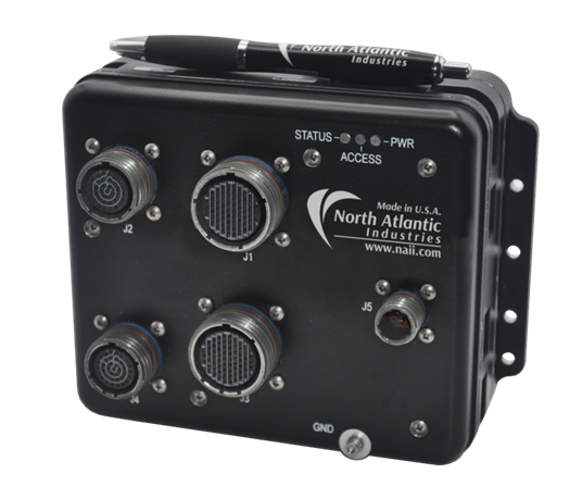
Figure 1. NIU3A
Unpacking
The NIU3A packing materials were designed specifically for transport protection of the NIU3A. When receiving the shipment container, inspect packaging for any evidence of physical damage. If damage is evident, it is recommended that the carrier agent is present when opening the shipping container. It is further recommended that all packing material is retained in the event the NIU3A needs to be shipped elsewhere.
System/Chassis Identification
An identification label, indicating part number, unique serial number, and Ethernet PHY MACs / default IP address(es) is affixed to the back of the system chassis.
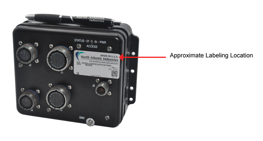
Figure 2. Unit Identification
Inspection
Inspect the chassis and connectors to ensure that they were not damaged during transit.
MECHANICAL INTERFACE
Mechanical Description
The NIU3A is a rugged, aluminum, conduction-cooled system. It must be mounted to a cold plate. The system thermal management design considerations should ensure that the chassis thermal interface (NIU3A bottom surface) does not exceed 71°C. Mounting holes are provided on the chassis bottom housing flanges (as depicted). See the outline drawing below.
Mounting Requirements
The NIU3A is conduction cooled and must be mounted in accordance with the drawing. The OID provides recommended hardware, torque, cold-plate flatness and surface finish specifications, and thermal conductivity requirements.
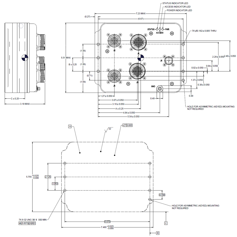
Figure 3. NIU3A Outline Dimensions/Cold Plate Mounting Pattern (Reference Only)
Notes:
- Unless otherwise specified, dimensions are in inches (mm); tolerances are:
- 2 PL DEC ±0.01; 3 PL DEC ±0.005
- FRACT ±1/64 (0.4); ANGLES ±1/2 (12.7)
Chassis (Earth) GND
Chassis ground point threaded insert location is on the connector side of the NIU3A as shown.
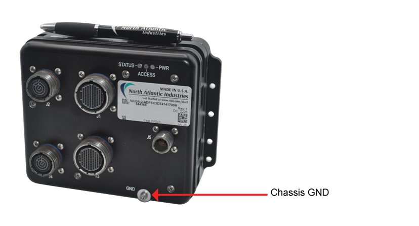
Figure 4. NIU3A Outline Dimensions/Chassis GND Location
Note
Chassis GND braid or equivalent to be secured by #6-32 screw/studs (with a depth of 0.3 inches) as end application requires. The NIU3A chassis is provided with #6-32 threaded insert only. The recommended torque for the NIU3A Chassis GND screw is 11 in-lbs. (125 N·cm)
CONNECTOR DESIGNATION & DESCRIPTION
The Power, I/O Interface and Ethernet connectors are located on the NIU3A front panel housing.
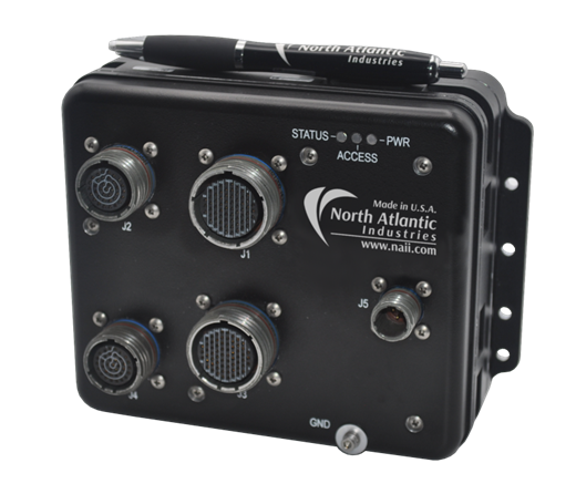
Figure 5. NIU3A (Front Panel Connector Placement)
Table 1. NIU3A Connector Designation and Description
| Connector Designation | Description |
| J1 | I/O Connector 1, Smart Module I/O Slot-1 & Slot-2 |
| J2 | 2x GbE, Maintenance, Debug (RS-232, System Reset) & extended processor option signals (RS-232, Hardware SATA Write Protect) |
| J3 | I/O Connector 2, Smart Module I/O Slot-3 & Onboard Discrete I/O |
| J4 | I/O Connector 3, Onboard ARINC-429, MIL-SDT-1553 & CANBus |
| J5 | Primary Power Connector, VDC |
Connector Details and Pinout
Generic pinout. See module I/O section or contact factory regarding any special module I/O configuration.
J1, I/O, Module-1 & Module-2
The J1 I/O connector supports Module-1 and Module-2 function I/O.
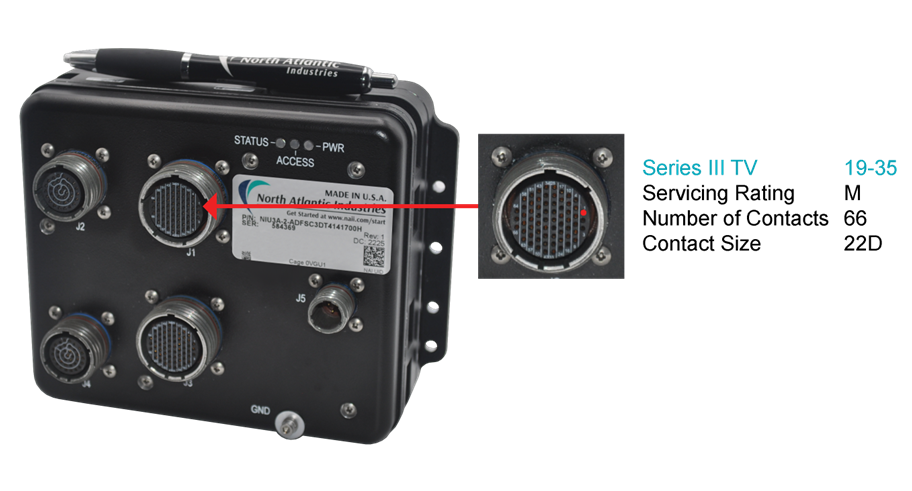
Figure 6. J1 I/O Module-1/-2 Connector Detail
Parts Identification
Table 2. J1 I/O Module-1/-2 Connector Definition
| Chassis (Box-level) | Mating Cable Connector | ||||
| Designation | MIL-DTL Equivalent Reference | Shell/Insert | Pin-count | MIL-DTL Equivalent Reference | NAI P/N (for reference) |
| J1 | D38999/20WF35SN | 19 / 35 | 66 | D38999/26WF35PN | 05-0284-COM |
Pinout
Generic pinout. See module I/O section or contact factory regarding any special module I/O configuration.
Table 3. J1 I/O Module-1/-2 Connector Pinout
| J1 Connector Pin | Signal | Notes |
| 24 | GND | Signal/System Ground |
| 59 | GND | Signal/System Ground |
| 39 | MOD1-DATIO01 | * |
| 45 | MOD1-DATIO02 | * |
| 58 | MOD1-DATIO03 | * |
| 38 | MOD1-DATIO04 | * |
| 44 | MOD1-DATIO05 | * |
| 51 | MOD1-DATIO06 | * |
| 36 | MOD1-DATIO07 | * |
| 43 | MOD1-DATIO08 | * |
| 31 | MOD1-DATIO09 | * |
| 35 | MOD1-DATIO10 | * |
| 22 | MOD1-DATIO11 | * |
| 25 | MOD1-DATIO12 | * |
| 18 | MOD1-DATIO13 | * |
| 19 | MOD1-DATIO14 | * |
| 4 | MOD1-DATIO15 | * |
| 14 | MOD1-DATIO16 | * |
| 21 | MOD1-DATIO17 | * |
| 23 | MOD1-DATIO18 | * |
| 26 | MOD1-DATIO19 | * |
| 13 | MOD1-DATIO20 | * |
| 7 | MOD1-DATIO21 | * |
| 15 | MOD1-DATIO22 | * |
| 29 | MOD1-DATIO23 | * |
| 16 | MOD1-DATIO24 | * |
| 37 | MOD1-DATIO25 | * |
| 52 | MOD1-DATIO26 | * |
| 30 | MOD1-DATIO27 | * |
| 34 | MOD1-DATIO28 | * |
| 27 | MOD1-DATIO29 | * |
| 28 | MOD1-DATIO30 | * |
| 9 | MOD1-DATIO31 | * |
| 3 | MOD1-DATIO32 | * |
| 54 | MOD2-DATIO01 | * |
| 46 | MOD2-DATIO02 | * |
| 47 | MOD2-DATIO03 | * |
| 62 | MOD2-DATIO04 | * |
| 48 | MOD2-DATIO05 | * |
| 55 | MOD2-DATIO06 | * |
| 57 | MOD2-DATIO07 | * |
| 40 | MOD2-DATIO08 | * |
| 41 | MOD2-DATIO09 | * |
| 49 | MOD2-DATIO10 | * |
| 32 | MOD2-DATIO11 | * |
| 42 | MOD2-DATIO12 | * |
| 6 | MOD2-DATIO13 | * |
| 12 | MOD2-DATIO14 | * |
| 5 | MOD2-DATIO15 | * |
| 10 | MOD2-DATIO16 | * |
| 1 | MOD2-DATIO17 | * |
| 17 | MOD2-DATIO18 | * |
| 8 | MOD2-DATIO19 | * |
| 20 | MOD2-DATIO20 | * |
| 64 | MOD2-DATIO21 | * |
| 60 | MOD2-DATIO22 | * |
| 61 | MOD2-DATIO23 | * |
| 66 | MOD2-DATIO24 | * |
| 63 | MOD2-DATIO25 | * |
| 56 | MOD2-DATIO26 | * |
| 50 | MOD2-DATIO27 | * |
| 33 | MOD2-DATIO28 | * |
| 2 | MOD2-DATIO29 | * |
| 11 | MOD2-DATIO30 | * |
| 65 | MOD2-DATIO31 | * |
| 53 | MOD2-DATIO32 | * |
Note
- = Module signal type is dependent on module function type fitted to slot.
J2, Ethernet Communication & Debug
The NIU3A supports up to two 10/100/1000Base-T ports (when appropriately configured) and debug/maintenance signals. The debug/maintenance signals provided are an RS-232 console port and System Reset (for a soft reset/reload). Additionally, typically for ARM/processor optioned configurations, a USB 2.0 port, Hardware Write Protect (for SATA accessibility) and a Real Time Clock Standby (i.e. auxiliary 3.3V/battery backup for the real time clock) are also provided.
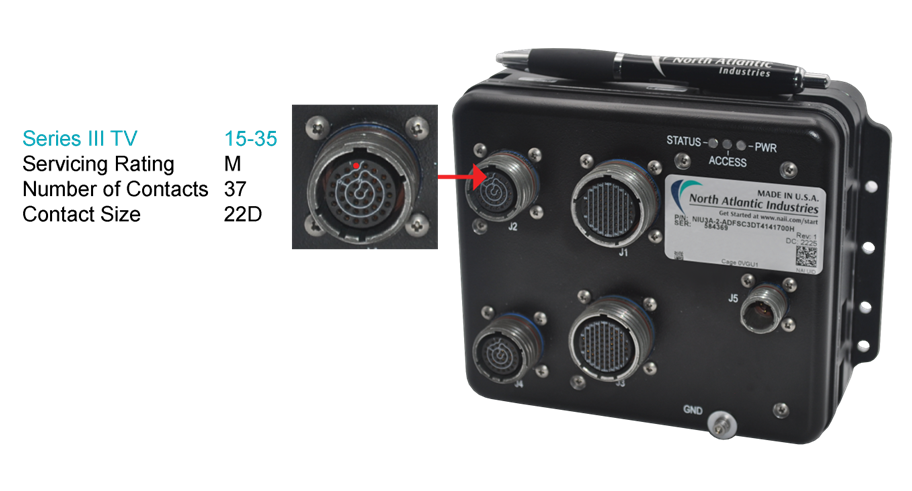
Figure 7. J2 Ethernet Communications & Debug Connector Detail
Parts Identification
Table 4. J2 Ethernet Communications & Debug Connector Definition
| Chassis (Box-level) | Mating Cable Connector | ||||
| Designation | MIL-DTL Equivalent Reference | Shell/Insert | Pin-count | MIL-DTL Equivalent Reference | NAI P/N (for reference) |
| J2 | D38999/20WD35SN | 15 / 35 | 37 | D38999/26WD35PN | 05-0302-COM |
Pinout
Table 5. J2 Ethernet Communications & Debug Connector Pinout
| J2 Connector Pin | Signal | Notes |
| 1 | ETH0-TP1+ | *8 |
| 2 | ETH0-TP2+ | *8 |
| 3 | ETH0-TP3+ | *8 |
| 4 | ETH0-TP3- | *8 |
| 5 | ENABLE | *4 |
| 6 | NVMRO | *3 |
| 7 | GND | *7 |
| 8 | GND | *7 |
| 9 | N/C | *9 |
| 10 | GND | *7 |
| 11 | I2C1-SCL | *6 |
| 12 | I2C1-SDA | *6 |
| 13 | SER0-TXD | *2 |
| 14 | SER0-RXD | *2 |
| 15 | N/C | |
| 16 | N/C | |
| 17 | USB0-D+ | *5 |
| 18 | ETH1-TP2- | *8 |
| 19 | ETH0-TP1- | *8 |
| 20 | ETH0-TP2- | *8 |
| 21 | GND | *7 |
| 22 | SYSRSTn | *1 |
| 23 | GND | *7 |
| 24 | GND | *7 |
| 25 | USB0-5V0 | *5 |
| 26 | N/C | |
| 27 | GND | *7 |
| 28 | ETH1-TP3- | *8 |
| 29 | USB0-D- | *5 |
| 30 | ETH1-TP2+ | *8 |
| 31 | ETH1-TP0- | *8 |
| 32 | ETH1-TP0+ | *8 |
| 33 | ETH0-TP0- | *8 |
| 34 | ETH0-TP0+ | *8 |
| 35 | ETH1-TP3+ | *8 |
| 36 | ETH1-TP1- | *8 |
| 37 | ETH1-TP1+ | *8 |
Notes
- SYSRSTn : An active “low” or GND logic level (as referenced to System GND of the NIU3A) assertion of the SYSRST# signal (internally pulled ‘high’) on the NIU3A processor and module cards will initiate an NIU3A system reset.
- Debug: RS-232 Serial Communications Console port
- NVMRO: Used for SATA Flash write enable/disable on the processor of the NIU3A. OPEN for Write Protect, GND for Write Enable.
- ENABLE: Used to power the PSU. OPEN for PSU Power-On, GND for PSU Power-Off.
- USB: USB 2.0 compatibility - accessible with processor accessible version of the NIU3A.(ARM option only).
- I2C1-Sxy: The two lines used for I2C communications. SCL (Serial Clock) synchronizes all data transfers over the I2C bus, SDA (Serial Data) carries the data.
- GND: All the identified GNDs are referenced to the same internal signal GND (System GND).
- ETHx-TPyz: Standard NIU3A configuration provides 2x 10/100/1000Base-T Ethernet ports
- N/C: Signals are undefined in the standard NIU3A configurations. These signals are considered no-connects (N/C).
J3, I/O, Module-3 & Onboard Discrete I/O (DT) Function
The J3 I/O connector supports Module-3 and Onboard Discrete (DT) function I/O.
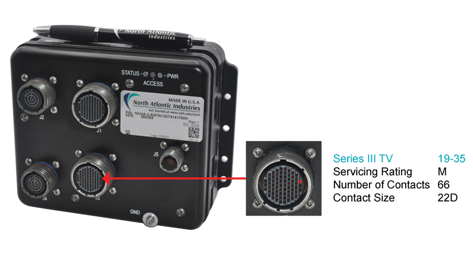
Figure 8. J3 I/O Module-3/Onboard Discrete Connector Detail
Parts Identification
Table 6. J3 I/O Module-3/Onboard Discrete Connector Definition
| Chassis (Box-level) | Mating Cable Connector | ||||
| Designation | MIL-DTL Equivalent Reference | Shell/Insert | Pin-count | MIL-DTL Equivalent Reference | NAI P/N (for reference) |
| J3 | D38999/20WF35SA | 19 / 35 | 66 | D38999/26WF35PA | 05-0285-COM |
Pinout
Generic pinout. See module I/O section or contact factory regarding any special module I/O configuration.
Table 7. J3 I/O Module-3/Onboard Discrete Connector Pinout
| J3 Connector Pin | Signal | Notes |
| 20 | DT-IO-CH01 | |
| 44 | DT-IO-CH02 | |
| 4 | DT-IO-CH03 | |
| 51 | DT-IO-CH04 | |
| 27 | DT-IO-CH05 | |
| 58 | DT-IO-CH06 | |
| 45 | DT-IO-CH07 | |
| 28 | DT-IO-CH08 | |
| 43 | DT-IO-CH09 | |
| 17 | DT-IO-CH10 | |
| 59 | DT-IO-CH11 | |
| 29 | DT-IO-CH12 | |
| 26 | DT-IO-CH13 | |
| 5 | DT-IO-CH14 | |
| 34 | DT-IO-CH15 | |
| 52 | DT-IO-CH16 | |
| 36 | DT-IO-CH17 | |
| 54 | DT-IO-CH18 | |
| 60 | DT-IO-CH19 | |
| 25 | DT-IO-CH20 | |
| 10 | DT-IO-CH21 | |
| 37 | DT-IO-CH22 | |
| 53 | DT-IO-CH23 | |
| 35 | DT-IO-CH24 | |
| 11 | DT-ISO-GND | |
| 19 | DT-ISO-GND | |
| 46 | DT-ISO-GND | |
| 47 | DT-ISO-GND | |
| 12 | DT-VCC1 | |
| 18 | DT-VCC2 | |
| 38 | DT-VCC3 | |
| 55 | DT-VCC4 | |
| 65 | MOD3-DATIO01 | * |
| 64 | MOD3-DATIO02 | * |
| 16 | MOD3-DATIO03 | * |
| 9 | MOD3-DATIO04 | * |
| 22 | MOD3-DATIO05 | * |
| 14 | MOD3-DATIO06 | * |
| 3 | MOD3-DATIO07 | * |
| 8 | MOD3-DATIO08 | * |
| 21 | MOD3-DATIO09 | * |
| 7 | MOD3-DATIO10 | * |
| 30 | MOD3-DATIO11 | * |
| 6 | MOD3-DATIO12 | * |
| 56 | MOD3-DATIO13 | * |
| 62 | MOD3-DATIO14 | * |
| 66 | MOD3-DATIO15 | * |
| 40 | MOD3-DATIO16 | * |
| 41 | MOD3-DATIO17 | * |
| 50 | MOD3-DATIO18 | * |
| 42 | MOD3-DATIO19 | * |
| 32 | MOD3-DATIO20 | * |
| 24 | MOD3-DATIO21 | * |
| 48 | MOD3-DATIO22 | * |
| 23 | MOD3-DATIO23 | * |
| 39 | MOD3-DATIO24 | * |
| 15 | MOD3-DATIO25 | * |
| 31 | MOD3-DATIO26 | * |
| 2 | MOD3-DATIO27 | * |
| 13 | MOD3-DATIO28 | * |
| 57 | MOD3-DATIO29 | * |
| 49 | MOD3-DATIO30 | * |
| 33 | MOD3-DATIO31 | * |
| 63 | MOD3-DATIO32 | * |
| 1 | SYS-GND | Signal/System Ground |
| 61 | SYS-GND | Signal/System Ground |
Note
- = Module signal type is dependent on module function type fitted to slot.
J4, I/O, Onboard ARINC-429/MIL-STD-1553/CANBus Functions
The J4 I/O connector supports onboard ARINC/MIL-STD/1553/CANBus function I/O.
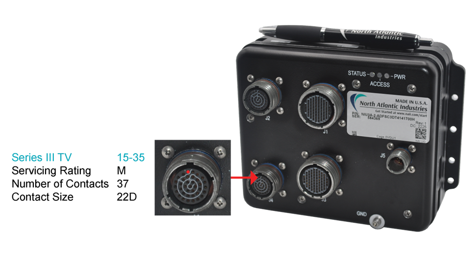
Figure 9. J4 I/O Onboard Functions Connector Detail
Parts Identification
Table 8. J4 I/O Onboard Functions Connector Definition
| Chassis (Box-level) | Mating Cable Connector | ||||
| Designation | MIL-DTL Equivalent Reference | Shell/Insert | Pin-count | MIL-DTL Equivalent Reference | NAI P/N (for reference) |
| J4 | D38999/20WD35SA | 15 / 35 | 37 | D38999/26WD35PA | 05-0532-COM |
Pinout
Generic pinout. See module I/O section or contact factory regarding any special module I/O configuration.
Table 9. J4 Onboard Functions Connector Pinout
| J4 Connector Pin | Signal | Notes |
| 7 | 1553-BUSA-CH1- | |
| 6 | 1553-BUSA-CH1+ | |
| 23 | 1553-BUSA-CH2- | |
| 33 | 1553-BUSA-CH2+ | |
| 25 | 1553-BUSB-CH1- | |
| 24 | 1553-BUSB-CH1+ | |
| 9 | 1553-BUSB-CH2- | |
| 8 | 1553-BUB-CH2+ | |
| 21 | AR429-CH1-A | |
| 22 | AR429-CH1-B | |
| 20 | AR429-CH2-A | |
| 31 | AR429-CH2-B | |
| 18 | AR429-CH3-A | |
| 30 | AR429-CH3-B | |
| 36 | AR429-CH4-A | |
| 37 | AR429-CH4-B | |
| 17 | AR429-CH5-A | |
| 29 | AR429-CH5-B | |
| 1 | AR429-CH6-A | |
| 19 | AR429-CH6-B | |
| 2 | AR429-CH7-A | |
| 3 | AR429-CH7-B | |
| 4 | AR429-CH8-A | |
| 5 | AR429-CH8-B | |
| 28 | CAN-CH1-H | |
| 27 | CAN-CH1-L | |
| 16 | CAN-CH2-H | |
| 15 | CAN-CH2-L | |
| 35 | CAN-CH3-H | |
| 34 | CAN-CH3-L | |
| 14 | CAN-CH4-H | |
| 13 | CAN-CH4-L | |
| 11 | GND-CAN1 | |
| 26 | GND-CAN2 | |
| 10 | GND-CAN3 | |
| 12 | GND-CAN4 | |
| 32 | N/C |
J5, Primary Power Connector
Primary input power is supported on the NIU3A via the J5 connector. Connectors used are as follows:
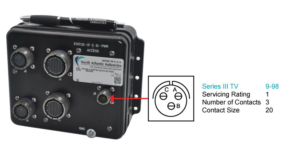
Figure 10. J5 Primary Power Connector Detail
Parts Identification
Table 10. J5 Primary Power Connector Definition
| Chassis (Box-level) | Mating Cable Connector | ||||
| Designation | MIL-DTL Equivalent Reference | Shell/Insert | Pin-count | MIL-DTL Equivalent Reference | NAI P/N (for reference) |
| J5 | D38999/20WA98PA (10,000 pF, incl. ‘c-filter') | 9 / 98 | 3 | D38999/26WA98SA | 05-0297-COM |
Pinout
Table 11. J5 Primary Power Connector Pinout
| J5 Connector Pin | Signal |
| A | Chassis GND |
| B | 28VDC-RTN |
| C | 28VDC |
POWER-UP & OPERATIONAL DESCRIPTION
Panel LEDs & Functions
Front Panel LEDs indications.
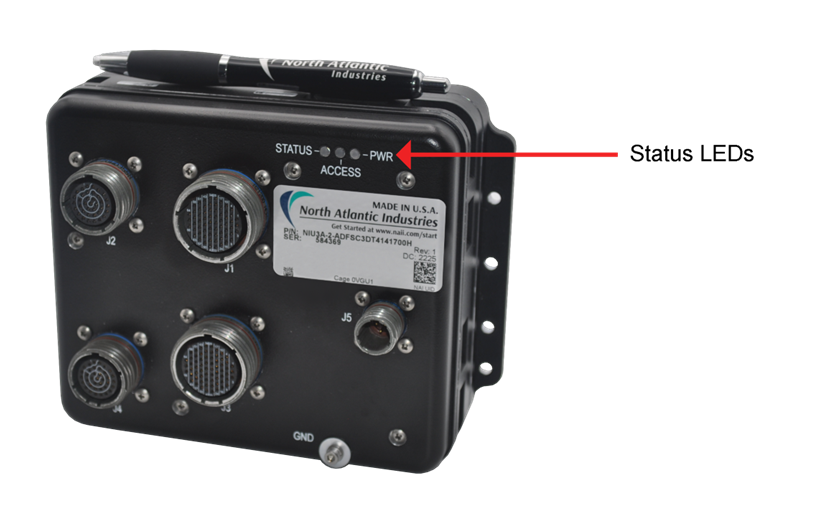
Figure 11. NIU3A Status LEDs Location
Table 12. NIU3A Status LEDs Function
| LED | STATUS / FUNCTION | |
| ILLUMINATED | EXTINGUISHED | |
| POWER GRN: | Blinking: Initializing Steady On: Power-On/Ready | Power-off |
| ACCESS YEL: | Blinking: Unit Access (GbE activity) | No Unit Access or Activity |
| STATUS RED: | Module BIT (Attention required) | No Module BIT Attention Required |
Basic Operations
Primary SBC/host/mission computer communications interface to the NIU3A is via the Gig-E port(s). Full command/control/register data query is requested and sent as a TCP/IP or UDP type message to the NIU3A via NAI Ethernet protocol structure, i.e. the NIU3A receives a message command and replies accordingly. In addition to direct read/write function module register access, once initialized the protocol can also support multi-register block read/writes as well as generate interrupt driven output messages or timed interval data ‘dump’ messages.
For detailed supplement, please visit the NAI web-site specific product page and refer to:
NAI Ethernet Interface for Embedded IO Boards Specification
The NIU3A is delivered as a tested unit. All operations have been verified. It is recommended that Power and Ethernet connections be made to verify operation of the function module(s) fitted within the NIU3A by making use of NAI’s “Embedded Soft Panel” (ESP), which can be utilized as a board/module level debugging tool (if the NIU3A function module(s) configuration supports). The example process shown below describes the use of NAI’s ESP Ethernet connectivity/exercising debug tool. Refer to the product web page software tab to download and access the latest ESP software package, including documentation, for the expected host operating system.
After applying appropriate power to the NIU3A, connect a Host computer (laptop or similar running e.g. Windows 7, Linux or other OS) and the ESP interface program application to either NIU3A Ethernet Port 1 or Port 2 (only for Dual Ethernet option). Type in the NIU’s default IP Address (e.g. 10.8.19.55 - see unit ID label for actual) and the screen below will display. The ESP is an interactive GUI application allowing full access, query and operation of the module(s) function(s) configured in the NIU3A.
Note
Referenced screenshots are examples and may not necessarily depict the latest version and/or revision of the NAI ESP. Please reference the latest ESP software and documentation available from the NAI web site.
Note
Ethernet port assignments and MAC address (factory default IP addresses are indicated on the system label). Please refer to the Configuration / Ordering information section of this document.

This screen shot shows that the “Board” is a NIU1A (NIU2A, etc.) and will interface over UDP. The particular IP address in this example is the default 192.168.1.6.
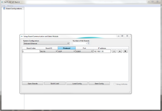
Additional operational windows will be dependent on the function modules installed. The ESP program, once communication has been established, can query the board (NIU3A) function module(s) configuration, and provides accessible function specific operating windows to allow full exercising of all the function programmable variables. Refer to the product web page software tab to download and access the latest ESP software package, including documentation, for the expected host operating system.
REGISTER MEMORY MAP ADDRESSING
The register map address consists of the following:
- cPCI/PCIe BAR or Base Address for the Board
- Module Slot Base Address
- Function Offset Address
Board Base Address
The table below lists the BAR used for access to the motherboard and module registers. The second BAR is used internally for motherboard and module firmware updates. The other cPCI/PCIe BARs not listed are not used.
| NAI Boards | Device ID | Bus | Motherboard and Module Register Access | Motherboard and Module Firmware Updates |
| Slave Boards | ||||
| NIU3A | N/A | N/A | Direct Memory Access | Internal Direct Memory Access |
Module Slot and Function Address
The NIU3A includes (4) basic preconfigured IO functions embedded within the motherboard (onboard functions). These functions are like the standard NAI COSA® smart functions identified as:
- CM5 = Support function ID; for 2 channels MIL-STD-1553 & 8 Channels ARINC 429/575 (combination functions)
- CBX = Support function ID; for 4 channels CAN Bus
- DT1/4 = Support function ID for 24-CH programmable Discrete I/O (standard/enhanced capability option)
Additionally, the NIU3A can be fitted with three additional function modules.
The following depicts the memory structure allocated for the (3) onboard function IDs and (3) configured functions
| NIU3A function/module structure/order: | |
| Function #1: | Expansion Module 1 |
| Function #2: | Expansion Module 2 |
| Function #3: | Expansion Module 3 |
| Function #4: | Onboard Function CM5-type (MIL-STD-1553, ARINC 429) |
| Function #5: | Onboard Function CBX-type (CAN Bus) |
| Function #6: | Onboard Function DT1/4-tpe (Discrete I/O) |
The “start” address of the function(s) on the NIU3A are factory pre-defined (and read from)) the Module Address register. Refer to Figure 12.
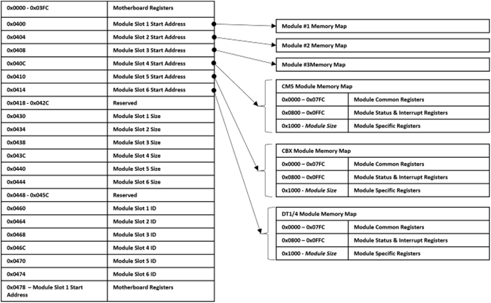
Figure 12. Register Memory Map Addressing Example for NIU3A
Address Calculation
Motherboard Registers:
Read/Write access to the motherboard registers starts with the base address for the board and then the motherboard base offset address.
For example, to address Module Slot 1 Start Address register (i.e. register address = 0x0400):
- Start with the base address for the board.
- Add the motherboard base register address offset.
| Motherboard Address = | Base Address + | Motherboard Address Offset | = 0x9000 0400 |
| 0x9000 0000 | 0x0400 |
Module Registers:
Read/Write access to the Function module’s registers start with the base address of the board. Add the “content” for the Module Start Address and then, add the specific module function register offset.
For example, to address an appropriate/specific function module with a register offset:
- Start with the base address for the board.
- Add the value (contents) from the module base address offset register (contents/value of Motherboard Memory register for Module 1 (i.e., @ 0x0400) = 0x4000.
- Then add the specific module function Register Offset of interest (i.e., 0x1000)
| (Function Specific) Address = | Base Address + | Module Base Address Offset + | Function Register Offset | = 0x9000 5000 |
| 0x9000 0000 | 0x4000 | 0x1000 |
REGISTER DESCRIPTIONS
Module Information Registers
The Module Slot Address, Module Slot Size and Module Slot ID provide information about the modules detected on the board.
| Module Slot Address | |
| Function: | Specifies the Base Address for the module in the specific slot position. |
| Type: | unsigned binary word (32-bit) |
| Data Range: | 0x0000 0000 to 0xFFFF FFFF |
| Read/Write: | R |
| Initialized Value: | Based on board's module configuration. |
| Operational Settings: | 0x0000 0000 indicates no Module found. |
| Module Slot Size | |
| Function: | Specifies the Memory Size (in bytes) allocated for the module in the specific slot position. |
| Type: | unsigned binary word (32-bit) |
| Range: | 0x0000 0000 to 0xFFFF FFFF |
| Read/Write: | R |
| Initialized Value: | Assigned by factory for the module. |
| Operational Settings: | 0x0000 0000 indicates no Module found. |
| Module Slot ID | |
| Function: | Specifies the Model ID for the module in the specified slot position. |
| Type: | 4-character ASCII string |
| Data Range: | 0x0000 0000 to 0xFFFF FFFF |
| Read/Write: | R |
| Initialized Value: | Assigned by factory for the module. |
| Operational Settings: | The Module ID is formatted as four ASCII bytes: three characters followed by a space. A value of 0000 0000 indicates no Module found. |
| D31 | D30 | D29 | D28 | D27 | D26 | D25 | D24 | D23 | D22 | D21 | D20 | D19 | D18 | D17 | D16 |
| ASCII Character (ex: 'A' - 0x41) | ASCII Character (ex: 'D' - 0x44) | ||||||||||||||
| D15 | D14 | D13 | D12 | D11 | D10 | D9 | D8 | D7 | D6 | D5 | D4 | D3 | D2 | D1 | D0 |
| ASCII Character (ex: '5' - 0x35) | ASCII Space (' ' - 0x20) | ||||||||||||||
Hardware Information Registers
The registers identified in this section provide information about the board’s hardware.
| Product Serial Number | |
| Function: | Specifies the Board Serial Number. |
| Type: | unsigned binary word (32-bit) |
| Data Range: | 0x0000 0000 to 0xFFFF FFFF |
| Read/Write: | R |
| Initialized Value: | Serial number assigned by factory for the board. |
| Operational Settings: | N/A |
| Platform | |
| Function: | Specifies the Board Platform Identifier. Values are for the ASCII characters for the NAI valid platforms (Identifiers). |
| Type: | 4-character ASCII string |
| Data Range: | See table below. |
| Read/Write: | R |
| Initialized Value: | ASCII code is for the Platform Identifier of the board |
| Operational Settings: | NAI platform for this board is shown below: |
| NAI Platform | Platform Identifier | 4-character ASCII string |
| NIU | 00 | 0x0000 3030 |
| Model | |
| Function: | Specifies the Board Model Identifier. Values are for the ASCII characters for the NAI valid models. |
| Type: | 4-character ASCII string |
| Data Range: | See table below. |
| Read/Write: | R |
| Initialized Value: | ASCII code is for the Model Identifier of the board |
| Operational Settings: | NAI model for this board is shown below: |
| NAI Model | 4-character ASCII string |
| NIU | 0x0055 494E |
| Generation | |
| Function: | Specifies the Board Generation Identifier. Values are for the ASCII characters for the NAI valid generation identifiers. |
| Type: | 4-character ASCII string |
| Data Range: | See table below. |
| Read/Write: | R |
| Initialized Value: | ASCII code is for the Generation Identifier of the board |
| Operational Settings: | NAI generation for this board is shown below: |
| NAI Generation | 4-character ASCII string |
| 3U | 0x0000 4133 |
| Processor Count/Ethernet Interface Count | |
| Function: | Specifies the Processor Count and Ethernet Interface Count |
| Type: | unsigned binary word (32-bit) |
| Data Range: | See table below. |
| Read/Write: | R |
| Operational Settings: | Processor Count - Indicates the number of unique processor types on the motherboard = 1 Ethernet Interface Count - Indicates the number of Ethernet interfaces on the product motherboard. For NIU3A, the Ethernet Interface Count is set for Dual Ethernet = 2 |
| D31 | D30 | D29 | D28 | D27 | D26 | D25 | D24 | D23 | D22 | D21 | D20 | D19 | D18 | D17 | D16 |
| Processor Count (0x0001) | |||||||||||||||
| D15 | D14 | D13 | D12 | D11 | D10 | D9 | D8 | D7 | D6 | D5 | D4 | D3 | D2 | D1 | D0 |
| Ethernet Interface Count (0x0002) | |||||||||||||||
| Maximum Module Slot Count/ARM Platform Type | |
| Function: | Specifies the Maximum Module Slot Count and ARM Platform Type. |
| Type: | unsigned binary word (32-bit) |
| Data Range: | See table below. |
| Read/Write: | R |
| Operational Settings: | See table below |
| NAI Board | Maximum Module Slot Count | ARM Platform Type | |
| Nano | NIU3A | 6 | UltraScale = 3 |
| D31 | D30 | D29 | D28 | D27 | D26 | D25 | D24 | D23 | D22 | D21 | D20 | D19 | D18 | D17 | D16 |
| Maximum Module Slot Count (0x0006) | |||||||||||||||
| D15 | D14 | D13 | D12 | D11 | D10 | D9 | D8 | D7 | D6 | D5 | D4 | D3 | D2 | D1 | D0 |
| ARM Platform Type (0x0003) | |||||||||||||||
Processor Operating System Registers
The registers in this section provide information about the Operating System that is running on the host processor on the motherboard. For boards that have more than one processor (ex. 75PPC1, 75INT2, 68PPC2, etc), the host processor would be the Power-PC or Intel processor.
| ARM Processor Platform | |
| Function: | Specifies the ARM Processor on the motherboard. Values are for the ASCII characters for the NAI host processor platforms specified by the Operating System. |
| Type: | 8-character ASCII string - Two (2) unsigned binary word (32-bit) |
| Data Range: | N/A |
| Read/Write: | R |
| Initialized Value: | ASCII code is for the Host Platform Identifier of the board |
| Operational Settings: | Valid NAI platforms based on Operating System loaded to host processor. |
| Processor Platform (Note: 8-character ASCII string) (“aarch64”) | |||||||||||||||
| Word 1 (0x6372 6161 = “craa”) | |||||||||||||||
| D31 | D30 | D29 | D28 | D27 | D26 | D25 | D24 | D23 | D22 | D21 | D20 | D19 | D18 | D17 | D16 |
| 'c' (0x63) | 'r' (0x72) | ||||||||||||||
| D15 | D14 | D13 | D12 | D11 | D10 | D9 | D8 | D7 | D6 | D5 | D4 | D3 | D2 | D1 | D0 |
| 'a' (0x61) | 'a' (0x61) | ||||||||||||||
| Word 2 (0x0034 3668 = “ 46h”) | |||||||||||||||
| D31 | D30 | D29 | D28 | D27 | D26 | D25 | D24 | D23 | D22 | D21 | D20 | D19 | D18 | D17 | D16 |
| null (0x00) | '4' (0x34) | ||||||||||||||
| D15 | D14 | D13 | D12 | D11 | D10 | D9 | D8 | D7 | D6 | D5 | D4 | D3 | D2 | D1 | D0 |
| '6' (0x36) | 'h' (0x68) | ||||||||||||||
| Processor Operating System | |
| Function: | Specifies the Operating System installed for the host processor. Values are for the ASCII characters for the NAI supported operating systems. |
| Type: | 12-character ASCII string - Three (3) unsigned binary word (32-bit) |
| Data Range: | N/A |
| Read/Write: | R |
| Operational Settings: | ASCII, 12 characters; ('Linux', 'VxWorks', 'RTOS', ...) |
| Processor Platform (Note: 12-character ASCII string) (“Linux”) | |||||||||||||||
| Word 1 (0x756E 694C = “uniL”) | |||||||||||||||
| D31 | D30 | D29 | D28 | D27 | D26 | D25 | D24 | D23 | D22 | D21 | D20 | D19 | D18 | D17 | D16 |
| 'u' (0x75) | 'n' (0x6E) | ||||||||||||||
| D15 | D14 | D13 | D12 | D11 | D10 | D9 | D8 | D7 | D6 | D5 | D4 | D3 | D2 | D1 | D0 |
| 'i' (0x69) | 'L' (0x4C) | ||||||||||||||
| Word 2 (0x0000 0078 = “ x”) | |||||||||||||||
| D31 | D30 | D29 | D28 | D27 | D26 | D25 | D24 | D23 | D22 | D21 | D20 | D19 | D18 | D17 | D16 |
| null (0x00) | null (0x00) | ||||||||||||||
| D15 | D14 | D13 | D12 | D11 | D10 | D9 | D8 | D7 | D6 | D5 | D4 | D3 | D2 | D1 | D0 |
| null (0x00) | 'x' (0x78) | ||||||||||||||
| Word 3 (0x0000 0000 = “ ”) | |||||||||||||||
| D31 | D30 | D29 | D28 | D27 | D26 | D25 | D24 | D23 | D22 | D21 | D20 | D19 | D18 | D17 | D16 |
| null (0x00) | null (0x00) | ||||||||||||||
| D15 | D14 | D13 | D12 | D11 | D10 | D9 | D8 | D7 | D6 | D5 | D4 | D3 | D2 | D1 | D0 |
| null (0x00) | null (0x00) | ||||||||||||||
Motherboard Firmware Information Registers
The registers in this section provide information on the revision of the firmware installed on the motherboard.
| Motherboard Core Firmware Version | |
| Function: | Specifies the Version of the NAI factory provided Motherboard Core Application installed on the board. |
| Type: | Two (2) unsigned binary word (32-bit) |
| Data Range: | 0x0000 0000 to 0xFFFF FFFF |
| Read/Write: | R |
| Operational Settings: | The motherboard firmware version consists of four components: Major, Minor, Minor 2 and Minor 3. |
| Motherboard Core Firmware Version (Note: little-endian order in register) (ex. 4.50.0.0) | |||||||||||||||
| Word 1 (Ex. 0050 0004 = 4.50 (Major.Minor) | |||||||||||||||
| D31 | D30 | D29 | D28 | D27 | D26 | D25 | D24 | D23 | D22 | D21 | D20 | D19 | D18 | D17 | D16 |
| Minor (ex: 0x0050 = 50) | |||||||||||||||
| D15 | D14 | D13 | D12 | D11 | D10 | D9 | D8 | D7 | D6 | D5 | D4 | D3 | D2 | D1 | D0 |
| Major (ex: 0x0004 = 4) | |||||||||||||||
| Word 2 (Ex. 0x0000 0000 = 0000 = 0.0 (Minor2.Minor3)) | |||||||||||||||
| D31 | D30 | D29 | D28 | D27 | D26 | D25 | D24 | D23 | D22 | D21 | D20 | D19 | D18 | D17 | D16 |
| Minor 3 (ex: 0x000 = 0) | |||||||||||||||
| D15 | D14 | D13 | D12 | D11 | D10 | D9 | D8 | D7 | D6 | D5 | D4 | D3 | D2 | D1 | D0 |
| Minor 2 (ex: 0x000 = 0) | |||||||||||||||
| Motherboard Firmware Build Date/Time | |
| Function: | Specifies the Build Date/Time of the NAI factory provided Motherboard Core Application installed on the board. |
| Type: | Two (2) unsigned binary word (32-bit) |
| Data Range: | N/A |
| Read/Write: | R |
| Operational Settings: | The motherboard firmware time consists of the Build Date and Build Time. |
| Motherboard Firmware Build Time (Note: little-endian order in register) | |||||||||||||||
| Word 1 - Build Date (ex. 0x1006 07E5 = 2021-6-16) | |||||||||||||||
| D31 | D30 | D29 | D28 | D27 | D26 | D25 | D24 | D23 | D22 | D21 | D20 | D19 | D18 | D17 | D16 |
| Day (ex: 0x10 = 1624) | Month (ex: 0x06 = 6) | ||||||||||||||
| D15 | D14 | D13 | D12 | D11 | D10 | D9 | D8 | D7 | D6 | D5 | D4 | D3 | D2 | D1 | D0 |
| Year (ex: 0x07E5 = 2021) | |||||||||||||||
| Word 2 - Build Time (ex. 0x001A 1A10 = 16:26:26) | |||||||||||||||
| D31 | D30 | D29 | D28 | D27 | D26 | D25 | D24 | D23 | D22 | D21 | D20 | D19 | D18 | D17 | D16 |
| null (0x00) | Seconds (ex: 0x1A = 26) | ||||||||||||||
| D15 | D14 | D13 | D12 | D11 | D10 | D9 | D8 | D7 | D6 | D5 | D4 | D3 | D2 | D1 | D0 |
| Minutes (ex: 0x1A = 26) | Hours (ex: 0x10 = 16) | ||||||||||||||
| Motherboard FPGA Firmware Version | |
| Function: | Specifies the Version of the NAI factory provided Motherboard FPGA installed on the board. |
| Type: | unsigned binary word (32-bit) |
| Data Range: | 0x0000 0000 to 0xFFFF FFFF |
| Read/Write: | R |
| Operational Settings: | The motherboard FPGA firmware version consists of two components: Major, Minor |
| Motherboard FPGA Firmware Version (ex. 0x0005 0009 = 5.9) | |||||||||||||||
| D31 | D30 | D29 | D28 | D27 | D26 | D25 | D24 | D23 | D22 | D21 | D20 | D19 | D18 | D17 | D16 |
| Major (ex: 0x0005 = 5) | |||||||||||||||
| D15 | D14 | D13 | D12 | D11 | D10 | D9 | D8 | D7 | D6 | D5 | D4 | D3 | D2 | D1 | D0 |
| Minor (ex: 0x0009 = 9) | |||||||||||||||
| Motherboard FPGA Firmware Compile Date/Time | |
| Function: | Specifies the Compile Date/Time of the NAI factory provided Motherboard FPGA installed on the board. |
| Type: | unsigned binary word (32-bit) |
| Data Range: | N/A |
| Read/Write: | R |
| Operational Settings: | The motherboard firmware time consists of the Build Date and Time in the following format: |
| Motherboard FPGA Compile Time (ex. 0xC32B 2923 = 06/24/21 18:36:35) | |||||||||||||||
| D31 | D30 | D29 | D28 | D27 | D26 | D25 | D24 | D23 | D22 | D21 | D20 | D19 | D18 | D17 | D16 |
| Day (D31:D27) | Month (D26:D23) | Year (D22:D17) | |||||||||||||
| ex. 0xC | ex. 0x3 | 0x2 | 0xB | ||||||||||||
| 1 | 1 | 0 | 0 | 0 | 0 | 1 | 1 | 0 | 0 | 1 | 0 | 1 | 0 | 1 | 10 |
| Day = 0x18 = 24 | Month = 0x6 = 6 | Year = 0x15 = 21 | |||||||||||||
| D15 | D14 | D13 | D12 | D11 | D10 | D9 | D8 | D7 | D6 | D5 | D4 | D3 | D2 | D1 | D0 |
| Hour (D16:D12) | Minutes (D11:D6) | Seconds (D5:D0) | |||||||||||||
| ex. 0x2 | ex. 0x9 | ex. 0x2B | ex. 0x3 | ||||||||||||
| 0 | 0 | 1 | 0 | 1 | 0 | 0 | 1 | 0 | 0 | 1 | 0 | 0 | 0 | 1 | 1 |
| Hour = 0x12 = 18 | Minutes = 0x24 = 36 | Seconds = 0x23 = 35 | |||||||||||||
Motherboard Monitoring Registers
The registers in this provide motherboard temperature measurement information.
Temperature Readings Register
The temperature registers provide the current, maximum (from power-up) and minimum (from power-up) for the processor and PCB for the UltraScale processor.
These registers are only available on Xilinx Generation 5 platforms, and are periodically populated by the motherboard core application, which only runs in Petalinux and BareMetal. For other operating systems, refer to the naibrd Software Support Kit (SSK) naibsp_system_Monitor_Temperature_Get() routine to manually retrieve the temperature (NOTE: this feature is typically utilized for development/factory use only; contact the factory for additional details on potential use, if required).
| Temperature Readings Register | |
| Function: | Specifies the Measured Temperatures on Motherboard. |
| Type: | signed byte (8-bits) for each temperature reading - Six (6) 32-bit words |
| Data Range: | 0x0000 0000 to 0xFFFF 0000 |
| Read/Write: | R |
| Initialized Value: | Value corresponding to the measured temperatures based on the table below. |
| Operational Settings: | The 8-bit temperature readings are signed bytes. For example, if the following register contains the value 0x0000 2B2B: |
Example:
| Word 1 (Current UltraScale Temperatures) | |||||||||||||||
| D31 | D30 | D29 | D28 | D27 | D26 | D25 | D24 | D23 | D22 | D21 | D20 | D19 | D18 | D17 | D16 |
| UltraScale Core Temperature | UltraScale PCB Temperature | ||||||||||||||
| D15 | D14 | D13 | D12 | D11 | D10 | D9 | D8 | D7 | D6 | D5 | D4 | D3 | D2 | D1 | D0 |
| 0x00 | 0x00 | ||||||||||||||
The values would represent the following temperatures:
| Temperature Measurements | Data Bits | Value | Temperature (Celsius) |
| UltraScale Core Temperature | D31:D24 | 0x2B | +43° |
| UltraScale PCB Temperature | D23:D16 | 0x2B | +43° |
| Temperature Readings | |||||||||||||||
| Word 1 (Current UltraScale Temperatures) | |||||||||||||||
| D31 | D30 | D29 | D28 | D27 | D26 | D25 | D24 | D23 | D22 | D21 | D20 | D19 | D18 | D17 | D16 |
| UltraScale Core Temperature | UltraScale PCB Temperature | ||||||||||||||
| D15 | D14 | D13 | D12 | D11 | D10 | D9 | D8 | D7 | D6 | D5 | D4 | D3 | D2 | D1 | D0 |
| 0x00 | 0x00 | ||||||||||||||
| Word 2 (Reserved) | |||||||||||||||
| D31 | D30 | D29 | D28 | D27 | D26 | D25 | D24 | D23 | D22 | D21 | D20 | D19 | D18 | D17 | D16 |
| 0x00 | 0x00 | ||||||||||||||
| D15 | D14 | D13 | D12 | D11 | D10 | D9 | D8 | D7 | D6 | D5 | D4 | D3 | D2 | D1 | D0 |
| 0x00 | 0x00 | ||||||||||||||
| Word 3 (Max UltraScale Temperatures) | |||||||||||||||
| D31 | D30 | D29 | D28 | D27 | D26 | D25 | D24 | D23 | D22 | D21 | D20 | D19 | D18 | D17 | D16 |
| Max UltraScale Core Temperature | Max UltraScale PCB Temperature | ||||||||||||||
| D15 | D14 | D13 | D12 | D11 | D10 | D9 | D8 | D7 | D6 | D5 | D4 | D3 | D2 | D1 | D0 |
| 0x00 | 0x00 | ||||||||||||||
| Word 4 (Reserved) | |||||||||||||||
| D31 | D30 | D29 | D28 | D27 | D26 | D25 | D24 | D23 | D22 | D21 | D20 | D19 | D18 | D17 | D16 |
| 0x00 | 0x00 | ||||||||||||||
| D15 | D14 | D13 | D12 | D11 | D10 | D9 | D8 | D7 | D6 | D5 | D4 | D3 | D2 | D1 | D0 |
| 0 | 0 | 0 | 0 | 0 | 0 | 0 | 0 | 0 | 0 | 0 | 0 | 0 | 0 | 0 | 0 |
| Word 5 (Min UltraScale Temperatures) | |||||||||||||||
| D31 | D30 | D29 | D28 | D27 | D26 | D25 | D24 | D23 | D22 | D21 | D20 | D19 | D18 | D17 | D16 |
| Min UltraScale Core Temperature | Min UltraScale PCB Temperature | ||||||||||||||
| D15 | D14 | D13 | D12 | D11 | D10 | D9 | D8 | D7 | D6 | D5 | D4 | D3 | D2 | D1 | D0 |
| 0 | 0 | 0 | 0 | 0 | 0 | 0 | 0 | 0 | 0 | 0 | 0 | 0 | 0 | 0 | 0 |
| Word 6 (Reserved) | |||||||||||||||
| D31 | D30 | D29 | D28 | D27 | D26 | D25 | D24 | D23 | D22 | D21 | D20 | D19 | D18 | D17 | D16 |
| 0x00 | 0x00 | ||||||||||||||
| D15 | D14 | D13 | D12 | D11 | D10 | D9 | D8 | D7 | D6 | D5 | D4 | D3 | D2 | D1 | D0 |
| 0 | 0 | 0 | 0 | 0 | 0 | 0 | 0 | 0 | 0 | 0 | 0 | 0 | 0 | 0 | 0 |
Higher Precision Temperature Readings Registers
These registers provide higher precision readings of the current UltraScale Core and PCB temperatures.
| Higher Precision UltraScale Core Temperature | |
| Function: | Specifies the Higher Precision Measured UltraScale Core temperature on Motherboard Board. |
| Type: | signed word (16-bits) for integer part and unsigned word (16-bits) for fractional part |
| Data Range: | 0x0000 0000 to 0xFFFF FFFF |
| Read/Write: | R |
| Initialized Value: | Measured UltraScale Core temperature on Motherboard Board |
| Operational Settings: | The upper 16-bits represent the signed integer part of the temperature and the lower 16-bits represent the fractional part of the temperature with the resolution of 1/1000 of degree Celsius. For example, if the register contains the value 0x002B 02FF, this represents UltraScale Core Temperature = 43.767° Celsius, and value 0xFFF6 0177 represents -10.375° Celsius. |
| D31 | D30 | D29 | D28 | D27 | D26 | D25 | D24 | D23 | D22 | D21 | D20 | D19 | D18 | D17 | D16 |
| Signed Integer Part of Temperature | |||||||||||||||
| D15 | D14 | D13 | D12 | D11 | D10 | D9 | D8 | D7 | D6 | D5 | D4 | D3 | D2 | D1 | D0 |
| Fractional Part of Temperature | |||||||||||||||
| Higher Precision Motherboard PCB Temperature | |
| Function: | Specifies the Higher Precision Measured Motherboard PCB temperature. |
| Type: | signed word (16-bits) for integer part and unsigned word (16-bits) for fractional part |
| Data Range: | 0x0000 0000 to 0xFFFF FFFF |
| Read/Write: | R |
| Initialized Value: | Measured Motherboard PCB temperature |
| Operational Settings: | The upper 16-bits represent the signed integer part of the temperature and the lower 16-bits represent the fractional part of the temperature with the resolution of 1/1000 of degree Celsius. For example, if the register contains the value 0x002B 02FF, this represents Interface PCB Temperature = 43.767° Celsius, and value 0xFFE8 036B represents -24.875° Celsius. |
| D31 | D30 | D29 | D28 | D27 | D26 | D25 | D24 | D23 | D22 | D21 | D20 | D19 | D18 | D17 | D16 |
| Signed Integer Part of Temperature | |||||||||||||||
| D15 | D14 | D13 | D12 | D11 | D10 | D9 | D8 | D7 | D6 | D5 | D4 | D3 | D2 | D1 | D0 |
| Fractional Part of Temperature | |||||||||||||||
Motherboard Health Monitoring Registers
The registers in this section provide a summary of motherboard temperature sensors and their corresponding bits. Additionally, this section provides an overview of the registers allocated to those sensors, which are used to monitor current/minimum/maximum temperature readings, upper & lower critical/warning temperature thresholds, and whether or not a programmed temperature threshold has been exceeded.
These registers are only available on Xilinx Generation 5 platforms, and are periodically populated by the motherboard core application, which only runs in Petalinux and BareMetal. For other operating systems, refer to the naibrd Software Support Kit (SSK) naibsp_system_Monitor_Temperature_Get() routine to manually retrieve the temperature (NOTE: this feature is typically utilized for development/factory use only; contact the factory for additional details on potential use, if required).
| Motherboard Sensor Summary Alarm | |
| Function: | The corresponding sensor bit is set if the sensor has crossed any of its thresholds. |
| Type: | unsigned binary word (32-bits) |
| Data Range: | See table below |
| Read/Write: | R |
| Initialized Value: | 0 |
| Operational Settings: | This register provides a summary for motherboard sensors. When the corresponding sensor bit is set, the Sensor Threshold Status register for that sensor will indicate the threshold condition that triggered the event. |
| Bit(s) | Sensor |
| D31:D5 | Reserved |
| D4 | Motherboard PCB Temperature |
| D3 | US+ Core Temperature |
| D2:D0 | Reserved |
Motherboard Sensor Registers
The registers listed in this section apply to each module sensor listed for the Motherboard Sensor Summary Status register. Each individual sensor register provides a group of registers for monitoring motherboard temperatures readings. From these registers, a user can read the current temperature of the sensor in addition to the minimum and maximum temperature readings since power-up. Upper and lower critical/warning temperature thresholds can be set and monitored from these registers. When a programmed temperature threshold is crossed, the Sensor Threshold Status register will set the corresponding bit for that threshold. The figure below shows the functionality of this group of registers when accessing the UltraScale Core Temperature sensor as an example.

| Sensor Threshold Status | |
| Function: | Reflects which threshold has been crossed |
| Type: | unsigned binary word (32-bits) |
| Data Range: | See table below |
| Read/Write: | R |
| Initialized Value: | 0 |
| Operational Settings: | The associated bit is set when the sensor reading exceed the corresponding threshold settings. |
| Bit(s) | Description |
| D31:D4 | Reserved |
| D3 | Exceeded Upper Critical Threshold |
| D2 | Exceeded Upper Warning Threshold |
| D1 | Exceeded Lower Critical Threshold |
| D0 | Exceeded Lower Warning Threshold |
| Sensor Current Reading | |
| Function: | Reflects current reading of temperature sensor |
| Type: | Single Precision Floating Point Value (IEEE-754) |
| Data Range: | Single Precision Floating Point Value (IEEE-754) |
| Read/Write: | R |
| Initialized Value: | N/A |
| Operational Settings: | The register represents current sensor reading as a single precision floating point value. For example, for a temperature sensor, register value 0x41C6 0000 represents temperature = 24.75° Celsius. |
| Sensor Minimum Reading | |
| Function: | Reflects minimum value of temperature sensor since power up |
| Type: | Single Precision Floating Point Value (IEEE-754) |
| Data Range: | Single Precision Floating Point Value (IEEE-754) |
| Read/Write: | R |
| Initialized Value: | N/A |
| Operational Settings: | The register represents minimum sensor value as a single precision floating point value. For example, for a temperature sensor, register value 0x41C6 0000 represents temperature = 24.75° Celsius. |
| Sensor Maximum Reading | |
| Function: | Reflects maximum value of temperature/voltage/current sensor since power up |
| Type: | Single Precision Floating Point Value (IEEE-754) |
| Data Range: | Single Precision Floating Point Value (IEEE-754) |
| Read/Write: | R |
| Initialized Value: | N/A |
| Operational Settings: | The register represents maximum sensor value as a single precision floating point value. For example, for a temperature sensor, register value 0x41C6 0000 represents temperature = 24.75° Celsius. |
| Sensor Lower Warning Threshold | |
| Function: | Reflects lower warning threshold of temperature sensor |
| Type: | Single Precision Floating Point Value (IEEE-754) |
| Data Range: | Single Precision Floating Point Value (IEEE-754) |
| Read/Write: | R/W |
| Initialized Value: | Default lower warning threshold (value dependent on specific sensor) |
| Operational Settings: | The register represents sensor lower warning threshold as a single precision floating point value. For example, for a temperature sensor, register value 0xC220 0000 represents temperature = -40.0° Celsius. |
| Sensor Lower Critical Threshold | |
| Function: | Reflects lower critical threshold of temperature sensor |
| Type: | Single Precision Floating Point Value (IEEE-754) |
| Data Range: | Single Precision Floating Point Value (IEEE-754) |
| Read/Write: | R/W |
| Initialized Value: | Default lower critical threshold (value dependent on specific sensor) |
| Operational Settings: | The register represents sensor lower critical threshold as a single precision floating point value. For example, for a temperature sensor, register value 0xC25C 0000 represents temperature = -55.0° Celsius. |
| Sensor Upper Warning Threshold | |
| Function: | Reflects upper warning threshold of temperature sensor |
| Type: | Single Precision Floating Point Value (IEEE-754) |
| Data Range: | Single Precision Floating Point Value (IEEE-754) |
| Read/Write: | R/W |
| Initialized Value: | Default upper warning threshold (value dependent on specific sensor) |
| Operational Settings: | The register represents sensor upper warning threshold as a single precision floating point value. For example, for a temperature sensor, register value 0x42AA 0000 represents temperature = 85.0° Celsius. |
| Sensor Upper Critical Threshold | |
| Function: | Reflects upper critical threshold of temperature sensor |
| Type: | Single Precision Floating Point Value (IEEE-754) |
| Data Range: | Single Precision Floating Point Value (IEEE-754) |
| Read/Write: | R/W |
| Initialized Value: | Default upper critical threshold (value dependent on specific sensor) |
| Operational Settings: | The register represents sensor upper critical threshold as a single precision floating point value. For example, for a temperature sensor, register value 0x42FA 0000 represents temperature = 125.0° Celsius. |
Ethernet Configuration Registers
The registers in this section provide information about the Ethernet Configuration for the two ports on the board.
Important
Regardless if the board is configured for one or two Ethernet ports, the second IP address cannot be on the same Subnet as the First IP Address. The table below provides examples of valid and invalid IP Addresses and Subnet Mask Addresses.
| First Port (A) IP Address | First Port (A) Subnet Mask | Second Port (B) IP Address | Second Port (B) Subnet Mask | Result |
| 192.168.1.5 | 255.255.255.0 | 192.168.2.5 | 255.255.255.0 | Good |
| 192.168.1.5 | 255.255.0.0 | 192.168.2.5 | 255.255.0.0 | Conflict |
| 192.168.1.5 | 255.255.0.0 | 192.168.2.5 | 255.255.255.0 | Conflict |
| 10.0.0.15 | 255.0.0.0 | 192.168.1.5 | 255.255.255.0 | Good |
| Ethernet MAC Address and Ethernet Settings | |
| Function: | Specifies the Ethernet MAC Address and Ethernet Settings for the Ethernet port. |
| Type: | Two (2) unsigned binary word (32-bit) |
| Data Range: | See table. |
| Read/Write: | R |
| Operational Settings: | The Ethernet MAC Address consists of six octets. The Ethernet Settings are defined in table. |
| Bits | Description | Values |
| D31:D23 | Reserved | 0 |
| D22:D21 | Duplex | 00 = Not Specified 01 = Half Duplex 10 = Full Duplex 11 = Reserved |
| D20:D18 | Speed | 000 = Not Specified 001 = 10 Mbps 010 = 100 Mbps 011 = 1000 Mbps 100 = 2500 Mbps 101 = 10000 Mbps 110 = Reserved 111 = Reserved |
| D17 | Auto Negotiate | 0 = Enabled 1 = Disabled |
| D16 | Static IP Address | 0 = Enabled 1 = Disabled |
| Ethernet MAC Address and Ethernet Settings (Note: little-endian order in register) | |||||||||||||||
| Word 1 (Ethernet MAC Address (Octets 1-4)) (ex: aa:bb:cc:dd:ee:ff) | |||||||||||||||
| D31 | D30 | D29 | D28 | D27 | D26 | D25 | D24 | D23 | D22 | D21 | D20 | D19 | D18 | D17 | D16 |
| MAC Address Octet 4 (ex: 0xDD) | MAC Address Octet 3 (ex: 0xCC) | ||||||||||||||
| D15 | D14 | D13 | D12 | D11 | D10 | D9 | D8 | D7 | D6 | D5 | D4 | D3 | D2 | D1 | D0 |
| MAC Address Octet 2 (ex: 0xBB) | MAC Address Octet 1 (ex: 0xAA) | ||||||||||||||
| Word 2 (Ethernet MAC Address (Octets 5-6) and Ethernet Settings) | |||||||||||||||
| D31 | D30 | D29 | D28 | D27 | D26 | D25 | D24 | D23 | D22 | D21 | D20 | D19 | D18 | D17 | D16 |
| Ethernet Settings (See table) | |||||||||||||||
| D15 | D14 | D13 | D12 | D11 | D10 | D9 | D8 | D7 | D6 | D5 | D4 | D3 | D2 | D1 | D0 |
| MAC Address Octet 6 (ex: 0xFF) | MAC Address Octet 5 (ex: 0xEE) | ||||||||||||||
| Ethernet Interface Name | |
| Function: | Specifies the Ethernet Interface Name for the Ethernet port. |
| Type: | 8-character ASCII string |
| Data Range: | See table. |
| Read/Write: | R |
| Operational Settings: | The Ethernet Interface Name (eth0, eth1, etc) for the Ethernet port. |
| Ethernet Interface Name (Note: ascii string in register) (ex. “eth0”) | |||||||||||||||
| Word 1 (Bit 0-31) (ex: 0x3068 7465 = “0hte”) | |||||||||||||||
| D31 | D30 | D29 | D28 | D27 | D26 | D25 | D24 | D23 | D22 | D21 | D20 | D19 | D18 | D17 | D16 |
| ASCII Character (ex: '0' - 0x30) | ASCII Character (ex: 'h' - 0x68) | ||||||||||||||
| D15 | D14 | D13 | D12 | D11 | D10 | D9 | D8 | D7 | D6 | D5 | D4 | D3 | D2 | D1 | D0 |
| ASCII Character (ex: 't' - 0x74) | ASCII Character (ex: 'e' - 0x65) | ||||||||||||||
| Word 2 (Bit 32-63) (ex: 0x0000 0000) | |||||||||||||||
| D31 | D30 | D29 | D28 | D27 | D26 | D25 | D24 | D23 | D22 | D21 | D20 | D19 | D18 | D17 | D16 |
| ASCII Character (ex: null - 0x00) | ASCII Character (ex: null - 0x00) | ||||||||||||||
| D15 | D14 | D13 | D12 | D11 | D10 | D9 | D8 | D7 | D6 | D5 | D4 | D3 | D2 | D1 | D0 |
| ASCII Character (ex: null - 0x00) | ASCII Character (ex: null - 0x00) | ||||||||||||||
| Ethernet IPv4 Address | |
| Function: | Specifies the Ethernet IPv4 Address for the Ethernet port. |
| Type: | Three (3) unsigned binary word (32-bit) |
| Data Range: | See table. |
| Read/Write: | R |
| Operational Settings: | The Ethernet IPv4 Address consists of three parts: IPv4 Address, IPv4 Subnet Mask and IPv4 Gateway. |
| Ethernet IPv4 Address (Note: little-endian order in register) | |||||||||||||||
| Word 1 (Ethernet IPv4 Address) (ex: 0x1001 A8C0 = 192.168.1.16) | |||||||||||||||
| D31 | D30 | D29 | D28 | D27 | D26 | D25 | D24 | D23 | D22 | D21 | D20 | D19 | D18 | D17 | D16 |
| IPv4 Address Octet 4 (ex: 0x10 = 16) | IPv4 Address Octet 3 (ex: 0x01 = 1) | ||||||||||||||
| D15 | D14 | D13 | D12 | D11 | D10 | D9 | D8 | D7 | D6 | D5 | D4 | D3 | D2 | D1 | D0 |
| IPv4 Address Octet 2 (ex: 0xA8 = 168) | IPv4 Address Octet 1 (ex: 0xC0 = 192) | ||||||||||||||
| Word 2 (Ethernet IPv4 Subnet) (ex: 0x00FF FFFF = 255.255.255.0) | |||||||||||||||
| D31 | D30 | D29 | D28 | D27 | D26 | D25 | D24 | D23 | D22 | D21 | D20 | D19 | D18 | D17 | D16 |
| IPv4 Subnet Octet 4 (ex: 0x00 = 0) | IPv4 Subnet Octet 3 (ex: 0xFF = 255) | ||||||||||||||
| D15 | D14 | D13 | D12 | D11 | D10 | D9 | D8 | D7 | D6 | D5 | D4 | D3 | D2 | D1 | D0 |
| IPv4 Subnet Octet 2 (ex: 0xFF = 255) | IPv4 Subnet Octet 1 (ex: 0xFF = 255) | ||||||||||||||
| Word 3 (Ethernet IPv4 Gateway) (ex: 0x0101 A8C0 = 192.168.1.1) | |||||||||||||||
| D31 | D30 | D29 | D28 | D27 | D26 | D25 | D24 | D23 | D22 | D21 | D20 | D19 | D18 | D17 | D16 |
| IPv4 Gateway Octet 4 (ex: 0x01 = 1) | IPv4 Gateway Octet 3 (ex: 0x01 = 1) | ||||||||||||||
| D15 | D14 | D13 | D12 | D11 | D10 | D9 | D8 | D7 | D6 | D5 | D4 | D3 | D2 | D1 | D0 |
| IPv4 Gateway Octet 2 (ex: 0xA8 = 168) | IPv4 Gateway Octet 1 (ex: 0xC0 = 192) | ||||||||||||||
| Ethernet IPv6 Address | |
| Function: | Specifies the Ethernet IPv6 Address for the Ethernet port. |
| Type: | Five (5) unsigned binary word (32-bit) |
| Data Range: | See table. |
| Read/Write: | R |
| Operational Settings: | The IPv6 Prefix length indicates the network portion of an IPv6 address using the following format:
|
The following is an illustration of IPv6 addressing with IPv6 Prefix length of 64.
| 64 bits | 64 bits | ||||||
| Prefix | Interface ID | ||||||
| Prefix 1 | Prefix 2 | Prefix 3 | Subnet ID | Interface ID 1 | Interface ID 2 | Interface ID 3 | Interface ID 4 |
| Example: 2002:c0a8:101:0:7c99:d118:9058:1235/64 | |||||||
| 2002 | C0A8 | 0101 | 0000 | 7C99 | D118 | 9058 | 1235 |
| Ethernet IPv6 Address (Note: little-endian order within 32-bit and 16-bit words in register) (ex. IPv6 Address: 2002:c0a8:201:0:7c99:d118:9058:1235 IPv6 Prefix: 64) | |||||||||||||||
| Word 1 (Ethernet IPv6 Address (Prefix 1-2)) (ex:0xA8C0 0220 = 2002 C0A8) | |||||||||||||||
| D31 | D30 | D29 | D28 | D27 | D26 | D25 | D24 | D23 | D22 | D21 | D20 | D19 | D18 | D17 | D16 |
| Prefix 2 (ex: 0xA8C0 = C0A8) | |||||||||||||||
| D15 | D14 | D13 | D12 | D11 | D10 | D9 | D8 | D7 | D6 | D5 | D4 | D3 | D2 | D1 | D0 |
| Prefix 1 (ex: 0x0220 = 2002) | |||||||||||||||
| Word 2 (Ethernet IPv6 Address (Prefix 3/Subnet ID)) (ex:0x000 0201 = 0201 0000) | |||||||||||||||
| D31 | D30 | D29 | D28 | D27 | D26 | D25 | D24 | D23 | D22 | D21 | D20 | D19 | D18 | D17 | D16 |
| Subnet ID (ex: 0x0000 = 0000) | |||||||||||||||
| D15 | D14 | D13 | D12 | D11 | D10 | D9 | D8 | D7 | D6 | D5 | D4 | D3 | D2 | D1 | D0 |
| Prefix 3 (ex: 0x0201 = 0201) | |||||||||||||||
| Word 3 (Ethernet IPv6 Address (Interface ID 1-2)) (ex: 0x18D1 997C = 7C99 D118) | |||||||||||||||
| D31 | D30 | D29 | D28 | D27 | D26 | D25 | D24 | D23 | D22 | D21 | D20 | D19 | D18 | D17 | D16 |
| Interface ID 2 (ex: 0x18D1 = D118) | |||||||||||||||
| D15 | D14 | D13 | D12 | D11 | D10 | D9 | D8 | D7 | D6 | D5 | D4 | D3 | D2 | D1 | D0 |
| Interface ID 1 (ex: 0x997C = 7C99) | |||||||||||||||
| Word 4 (Ethernet IPv6 Address (Interface ID 3-4)) (ex: 0x3512 5890 = 9058 1235) | |||||||||||||||
| D31 | D30 | D29 | D28 | D27 | D26 | D25 | D24 | D23 | D22 | D21 | D20 | D19 | D18 | D17 | D16 |
| Interface ID 4 (ex: 0x3512 = 1235) | |||||||||||||||
| D15 | D14 | D13 | D12 | D11 | D10 | D9 | D8 | D7 | D6 | D5 | D4 | D3 | D2 | D1 | D0 |
| Interface ID 3 (ex: 0x5890 = 9058) | |||||||||||||||
| Word 5 (Ethernet IPv6 Prefix Length) (ex:0x0000 0040) | |||||||||||||||
| D31 | D30 | D29 | D28 | D27 | D26 | D25 | D24 | D23 | D22 | D21 | D20 | D19 | D18 | D17 | D16 |
| 0 | 0 | 0 | 0 | 0 | 0 | 0 | 0 | 0 | 0 | 0 | 0 | 0 | 0 | 0 | 0 |
| D15 | D14 | D13 | D12 | D11 | D10 | D9 | D8 | D7 | D6 | D5 | D4 | D3 | D2 | D1 | D0 |
| Prefix Length (ex: 0x0040 = 64) | |||||||||||||||
Interrupt Vector and Steering
When interrupts are enabled, the interrupt vector associated with the specific interrupt can be programmed (typically with a unique number/identifier) such that it can be utilized in the Interrupt Service Routine (ISR) to identify the type of interrupt. When an interrupt occurs, the contents of the Interrupt Vector registers is reported as part of the interrupt mechanism. In addition to specifying the interrupt vector, the interrupt can be directed (“steered”) to the native bus or to the application running on the onboard ARM processor.
Note
The Interrupt Vector and Interrupt Steering registers are mapped to the Motherboard Common Memory and these registers are associated with the Module Slot position (refer to Function Register Map).
| Interrupt Vector | |
| Function: | Set an identifier for the interrupt. |
| Type: | unsigned binary word (32-bit) |
| Data Range: | 0x0000 0000 to 0xFFFF FFFF |
| Read/Write: | R/W |
| Initialized Value: | 0 |
| Operational Settings: | When an interrupt occurs, this value is reported as part of the interrupt mechanism. |
| Interrupt Steering | |
| Function: | Sets where to direct the interrupt. |
| Type: | unsigned binary word (32-bit) |
| Data Range: | See table |
| Read/Write: | R/W |
| Initialized Value: | 0 |
| Operational Settings: | When an interrupt occurs, the interrupt is sent as specified: |
| Direct Interrupt to VME | 1 |
| Direct Interrupt to ARM Processor (via SerDes) (Custom App on ARM or NAI Ethernet Listener App) | 2 |
| Direct Interrupt to PCIe Bus | 5 |
| Direct Interrupt to cPCI Bus | 6 |
Modules Health Monitoring Registers
| Module BIT Status | |
| Function: | Provides the ability to monitor the individual Module BIT Status. |
| Type: | unsigned binary word (32-bit) |
| Data Range: | 0x0000 0000 to 0xFFFF FFFF |
| Read/Write: | R |
| Operational Settings: | The Module BIT Status registers provide the ability to monitor individual Module BIT results as Latched and current value. A 1 is any bit field indicates BIT failure for the Module in that slot. |
| Bit(s) | Description |
| D31:D23 | Reserved |
| D22 | Module Slot 6 BIT Failure (current value) |
| D21 | Module Slot 5 BIT Failure (current value) |
| D20 | Module Slot 4 BIT Failure (current value) |
| D19 | Module Slot 3 BIT Failure (current value) |
| D18 | Module Slot 2 BIT Failure (current value) |
| D17 | Module Slot 1 BIT Failure (current value) |
| D16 | Reserved |
| D15:D7 | Reserved |
| D6 | Module Slot 6 BIT Failure - Latched |
| D5 | Module Slot 5 BIT Failure - Latched |
| D4 | Module Slot 4 BIT Failure - Latched |
| D3 | Module Slot 3 BIT Failure - Latched |
| D2 | Module Slot 2 BIT Failure - Latched |
| D1 | Module Slot 1 BIT Failure - Latched |
| D0 | Reserved |
Scratchpad Area
| Scratchpad Area | |
| Function: | Registers reserved as scratch pad for customer use. NOTE: this area is also used to copy results from FRAM so that data can be read via the PCIe bus. |
| Type: | unsigned binary word (32-bit) |
| Data Range: | 0x0000 0000 to 0xFFFF FFFF |
| Read/Write: | R/W |
| Operational Settings: | This area in memory is reserved for customer use or POST FRAM results. |
MOTHERBOARD FUNCTION REGISTER MAP
KEY
| Configuration/Control |
| Measurement/Status/Board Information |
| MODULE INFORMATION REGISTERS | |||||
| OFFSET | REGISTER NAME | ACCESS | OFFSET | REGISTER NAME | ACCESS |
| 0x0400 | Module Slot 1 Address | R | 0x0430 | Module Slot 1 Size | R |
| 0x0404 | Module Slot 2 Address | R | 0x0434 | Module Slot 2 Size | R |
| 0x0408 | Module Slot 3 Address | R | 0x0438 | Module Slot 3 Size | R |
| 0x040C | Module Slot 4 Address | R | 0x043C | Module Slot 4 Size | R |
| 0x0410 | Module Slot 5 Address | R | 0x0440 | Module Slot 5 Size | R |
| 0x0414 | Module Slot 6 Address | R | 0x0444 | Module Slot 6 Size | R |
| 0x0460 | Module Slot 1 ID | R | |||
| 0x0464 | Module Slot 2 ID | R | |||
| 0x0468 | Module Slot 3 ID | R | |||
| 0x046C | Module Slot 4 ID | R | |||
| 0x0470 | Module Slot 5 ID | R | |||
| 0x0474 | Module Slot 6 ID | R | |||
| HARDWARE INFORMATION REGISTERS | |||||
| OFFSET | REGISTER NAME | ACCESS | OFFSET | REGISTER NAME | ACCESS |
| 0x0020 | Product Serial Number | R | |||
| 0x0024 | Platform | R | 0x0030 | Processor Count/Ethernet Count | R |
| 0x0028 | Model | R | 0x0034 | Maximum Module Slot Count/ARM Platform Type | R |
| 0x002C | Generation | R | |||
| 0x0038 | Processor Platform (Bit 0-31) | R | 0x0040 | Processor Operating System (Bit 0-31) | R |
| 0x003C | Processor Platform (Bit 32-63) | R | 0x0044 | Processor Operating System (Bit 32-63) | R |
| 0x0048 | Processor Operating System (Bit 64-95) | R | |||
| 0x004C | Processor Operating System Version (Bit 0-31) | R | |||
| 0x0050 | Processor Operating System Version (Bit 32-63) | R | |||
| MOTHERBOARD FIRMWARE INFORMATION REGISTERS | |||||
| OFFSET | REGISTER NAME | ACCESS | OFFSET | REGISTER NAME | ACCESS |
| Motherboard Core Information | Motherboard FPGA Information | ||||
| 0x0100 | MB Core Major/Minor Version | R | 0x0270 | MB FPGA Revision | R |
| 0x0104 | MB Core Minor 2/3 Version | R | 0x0274 | MB FPGA Compile Date/Time | R |
| 0x0108 | MB Core Build Date (Bit 0-31) | R | |||
| 0x010C | MB Core Build Date (Bit 32-63) | R | |||
| MOTHERBOARD MEASUREMENTS REGISTERS | |||||
| OFFSET | REGISTER NAME | ACCESS | OFFSET | REGISTER NAME | ACCESS |
| Temperature Readings | High Precision Temperature Readings | ||||
| 0x0200 | Current UltraScale Temperatures | R | 0x0230 | Current UltraScale Core Temperature | R |
| 0x0204 | Reserved | R | 0x0234 | Current Motherboard PCB Temperature | R |
| 0x0208 | Max UltraScale Temp | R | |||
| 0x020C | Reserved | R | |||
| 0x0210 | Min UltraScale Temperatures | R | |||
| 0x0214 | Reserved | R | |||
| MOTHERBOARD HEALTH MONITORING REGISTERS | |||||
| OFFSET | REGISTER NAME | ACCESS | OFFSET | REGISTER NAME | ACCESS |
| 0x20F8 | Motherboard Sensor Summary Status | R | |||

| ETHERNET CONFIGURATION REGISTERS | |||||
| OFFSET | REGISTER NAME | ACCESS | OFFSET | REGISTER NAME | ACCESS |
| Ethernet A | Ethernet B | ||||
| 0x0070 | Ethernet A MAC (Octets 1-4) | R | 0x00A0 | Ethernet B MAC (Octets 1-4) | R |
| 0x0074 | Ethernet A MAC (Octets 5-6)/Misc Settings | R | 0x00A4 | Ethernet B MAC (Octets 5-6)/Misc Settings | R |
| 0x0078 | Ethernet A Interface Name (Bit 0-31) | R | 0x00A8 | Ethernet B Interface Name (Bit 0-31) | R |
| 0x007C | Ethernet A Interface Name (Bit 32-63) | R | 0x00AC | Ethernet B Interface Name (Bit 32-63) | R |
| 0x0080 | Ethernet A IPv4 Address | R | 0x00B0 | Ethernet B IPv4 Address | R |
| 0x0084 | Ethernet A IPv4 Subnet Mask | R | 0x00B4 | Ethernet B IPv4 Subnet Mask | R |
| 0x0088 | Ethernet A IPv4 Gateway | R | 0x00B8 | Ethernet B IPv4 Gateway | R |
| 0x008C | Ethernet A IPv6 Address (Prefix 1-2) | R | 0x00BC | Ethernet B IPv6 Address (Prefix 1-2) | R |
| 0x0090 | Ethernet A IPv6 Address (Prefix 3/Subnet ID) | R | 0x00C0 | Ethernet B IPv6 Address (Prefix 3/Subnet ID) | R |
| 0x0094 | Ethernet A IPv6 Address (Interface ID 1-2) | R | 0x00C4 | Ethernet B IPv6 Address (Interface ID 1-2) | R |
| 0x0098 | Ethernet A IPv6 Address (Interface ID 3-4) | R | 0x00C8 | Ethernet B IPv6 Address (Interface ID 3-4) | R |
| 0x009C | Ethernet A IPv6 Prefix Length | R | 0x00CC | Ethernet B IPv6 Prefix Length | R |
| INTERRUPT VECTOR AND STEERING | |||||
| OFFSET | REGISTER NAME | ACCESS | OFFSET | REGISTER NAME | ACCESS |
| 0x0500 - 0x057C | Module 1 Interrupt Vector 1 - 32 | R/W | 0x0600 - 0x067C | Module 1 Interrupt Steering 1 - 32 | R/W |
| 0x0700 - 0x077C | Module 2 Interrupt Vector 1 - 32 | R/W | 0x0800 - 0x087C | Module 2 Interrupt Steering 1 - 32 | R/W |
| 0x0900 - 0x097C | Module 3 Interrupt Vector 1 - 32 | R/W | 0x0A00 - 0x0A7C | Module 3 Interrupt Steering 1 - 32 | R/W |
| 0x0B00 - 0x0B7C | Module 4 Interrupt Vector 1 - 32 | R/W | 0x0C00 - 0x0C7C | Module 4 Interrupt Steering 1 - 32 | R/W |
| 0x0D00 - 0x0D7C | Module 5 Interrupt Vector 1 - 32 | R/W | 0x0E00 - 0x0E7C | Module 5 Interrupt Steering 1 - 32 | R/W |
| 0x0F00 - 0x0F7C | Module 6 Interrupt Vector 1 - 32 | R/W | 0x1000 - 0x107C | Module 6 Interrupt Steering 1 - 32 | R/W |
| MODULES HEALTH MONITORING REGISTERS | |||||
| OFFSET | REGISTER NAME | ACCESS | OFFSET | REGISTER NAME | ACCESS |
| 0x0128 | Module BIT Status (current and latched) | R | |||
| SCRATCHPAD REGISTERS | |||||
| OFFSET | REGISTER NAME | ACCESS | OFFSET | REGISTER NAME | ACCESS |
| 0x3800 - 0x3BFF | Scratchpad Registers | R/W | |||
ETHERNET
(For detailed supplement, please visit the NAI web-site specific product page and refer to: Ethernet Interface for Generation 5 SBC and Embedded IO Boards Specification)
Note
For products capable of 10/100/1000Base-KX functionality - the product Ethernet PHY supports 1000BASE-X. Product interoperability with 10/100/1000BASE-KX is supported with 1000BASE-X (provided that auto-negotiation is disabled).
The Ethernet Interface Option allows communications and control access to all function modules either via the system BUS or Ethernet ports 1 or 2.
Ethernet 1 Ethernet 2 Ethernet 3* Ethernet 4* (REF PORT A) (REF PORT B) (REF PORT C) (REF PORT D) The default IP address: 192.168.1.16 192.168.2.16 192.168.3.16 192.168.4.16 The default subnet: 255.255.255.0 255.255.255.0 255.255.255.0 255.255.255.0 The default gateway: 192.168.1.1 192.168.2.1 192.168.3.1 192.168.4.1 *see Part Number Designation for applicability.
Note
Actual “as shipped” card Ethernet default IP addresses may vary based upon final ATP configuration(s).
The NAI interface supports IPv4 and IPv6 and both the TCP and UDP protocols. The Ethernet Operation Mode Command Listener application running on the motherboard host processor implements the operation interface. The listener is operational on startup through the nai_MBStartup process and listen on specific ports for commands to process. The default ports are listed below:
- TCP1 - Port 52801
- TCP2 - Port 52802
- UDP1 - Port 52801
- UDP2 - Port 52802
While the listener is active, note that interrupts from the motherboard do not trigger. The listener can be disabled by turning off the nai_MBStartup process through the Motherboard EEPROM. To turn off nai_MBStartup use the command mbeeprom_util set MBStartupInitOnlyFlag 1 in the console, either by serial port or telnet to the motherboard, and then reboot the system. To turn on the nai_MBStartup use the command mbeeprom_util set MBStartupInitOnlyFlag 0 in the console, either by serial port or telnet to the motherboard, and then reboot the system.
Ethernet Message Framework
The interface uses a specific message framework for all commands and responses. All messages begin with a Preamble code and end with a Postamble code. The message framework is shown below.
Preamble
2 bytes
Always
0xD30FSequenceNo
2 bytesType Code
2 byteMessage Length
(2 bytes)Payload
(0..1414 bytes)Postamble
2 bytes
Always
0xF03DMessage Elements
Preamble The Preamble is used to delineate the beginning of a message frame.
The Preamble is always 0xD30F.SequenceNo The SequenceNo is used to associate Commands with Responses. Type Code Type Codes are used to define the type of Command or Response the message contains. Message Length The Message Length is the number of bytes in the complete message frame starting with and including the
Preamble and ending with and including the Postamble.Payload The Payload contains the unique data that makes up the command or response.
Payloads vary based on command type.Postamble The Postamble is use to delineate the end of a message frame.
The Postamble is always 0xF03D.Notes
- The messaging protocol applies only to card products.
- Messaging is managed by the connected (client) computer. The client computer will send a single message and wait for a reply from the card. Multiple cards may be managed from a single computer, subject to channel and computer capacity.
Board Addressing
The interface provides two main addressing areas: Onboard and Off-board.
Onboard addressing refers to accessing resources located on the board that is implementing the operation interface (including its modules).
Off-board addressing refers to accessing resources located on another board reachable via VME, PCI, or other bus. Off-board addressing requires a Master/Slave configuration.
The user must always specify if a particular address is Onboard or Off-board. See the command descriptions for the onboard and off-board flags.
Within a particular board (Onboard or Off-board), the address space is broken up into two areas: Motherboard Common Address Space and Module Address Space. All addresses are 32-bit.
Motherboard Common Address Space starts at 0x00000000 and ends at 0x00004000. This is a 4Kx32-bit address space (16 kbytes).
Module Address Space starts at 0x00004000. Module addressing is dynamically configured at startup. NAI boards support between 1 and 6 modules. The minimum module address space size is 4Kx32 (16 kbytes) and module sizes are always a multiple of 4Kx32.
Module addressing is dynamic and cumulative. The first detected module (starting with Slot 1) is given an address of 0x00004000. The 2nd detected Module is given an address of:
First_Detected_Module_Address + First_Detected_Module_Size
Note
Slots do not define addresses.
If no module is detected in a module slot, that slot is not given an address. Therefore, if the first detected Module is in Slot 2, then that module address will be 0x00004000. If the next detected module is in Slot 4, then the address of that Module will be:
Second_Detected_Module_Address = First_Detected_Module_Address + First_Detected_Module_Size
If a 3rd Module is detected in Slot 6, then the address of that Module will be:
Third_Detected_Module_Address = Second_Detected_Module_Address + Second_Detected_Module_Size
Note
Module addresses are calculated at each board startup when the modules are detected. Therefore, if a module should fail to be detected due to malfunction or because it was removed from the motherboard, the addresses of the modules that follow it in the slot sequence will be altered. This is important to note when programming to this interface.
Users can always retrieve the Module Addresses, Module Sizes and Module IDs from the fixed Motherboard Common address area. This data is set upon each board startup. While the Module Addressing is dynamic, the address where these addresses are stored is fixed. For example, to find the startup address of the module location in Slot 3, refer to the MB Common Address 0x00000408 from the Motherboard Common Addresses table that follows.
Ethernet Wiring Convention
Link to original
RJ-45 Pin T568A Color T568B Color 10/100Base-T 1000BASE-T NAI wiring convention 1 white/green stripe white/orange stripe TX+ DA+ ETH-TP0+ 2 green orange TX- DA- ETH-TP0- 3 white/orange stripe white/green stripe RX+ DB+ ETH-TP1+ 4 blue blue DC+ ETH-TP2+ 5 white/blue stripe white/blue stripe DC- ETH-TP2- 6 orange green RX- DB- ETH-TP1- 7 white/brown stripe white/brown stripe DD+ ETH-TP3+ 8 brown brown DD- ETH-TP3-
NIU3A I/O MAPPING
NIU3A I/O Mapping (for reference) is shown below, with respect to DATAIO. Additional information on pin-outs can be found in the Module Operational Manuals or by contacting the factory.
| MOD1 J1 - I/O | MOD2 J1 - I/O | MOD3 J3 - I/O | Internal Reference Only |
| 39 | 54 | 65 | MOD-DATIO01 |
| 45 | 46 | 64 | MOD-DATIO02 |
| 58 | 47 | 16 | MOD-DATIO03 |
| 38 | 62 | 9 | MOD-DATIO04 |
| 44 | 48 | 22 | MOD-DATIO05 |
| 51 | 55 | 14 | MOD-DATIO06 |
| 36 | 57 | 3 | MOD-DATIO07 |
| 43 | 40 | 8 | MOD-DATIO08 |
| 31 | 41 | 21 | MOD-DATIO09 |
| 35 | 49 | 7 | MOD-DATIO10 |
| 22 | 32 | 30 | MOD-DATIO11 |
| 25 | 42 | 6 | MOD-DATIO12 |
| 18 | 6 | 56 | MOD-DATIO13 |
| 19 | 12 | 62 | MOD-DATIO14 |
| 4 | 5 | 66 | MOD-DATIO15 |
| 14 | 10 | 40 | MOD-DATIO16 |
| 21 | 1 | 41 | MOD-DATIO17 |
| 23 | 17 | 50 | MOD-DATIO18 |
| 26 | 8 | 42 | MOD-DATIO19 |
| 13 | 20 | 32 | MOD-DATIO20 |
| 7 | 64 | 24 | MOD-DATIO21 |
| 15 | 60 | 48 | MOD-DATIO22 |
| 29 | 61 | 23 | MOD-DATIO23 |
| 16 | 66 | 39 | MOD-DATIO24 |
| 37 | 63 | 15 | MOD-DATIO25 |
| 52 | 56 | 31 | MOD-DATIO26 |
| 30 | 50 | 2 | MOD-DATIO27 |
| 34 | 33 | 13 | MOD-DATIO28 |
| 27 | 2 | 57 | MOD-DATIO29 |
| 28 | 11 | 49 | MOD-DATIO30 |
| 9 | 65 | 33 | MOD-DATIO31 |
| 3 | 53 | 63 | MOD-DATIO32 |
| N/C | |||
| N/C | |||
| N/C | |||
| 24 | 24 | 1 | SYSTEM GND |
| 59 | 59 | 61 | SYSTEM GND |
Key
| N/C | Indicates module signal pin not available at Jx I/O Connector. |
NIU3A PART NUMBER DESIGNATION
Click here for the NIU3A part number designation
SYNCHRO/RESOLVER AND LVDT/RVDT SIMULATION MODULE CODE TABLES
Select the Digital-to-Synchro (DSx), Digital-to-Resolver (DRx) or Digital-to-LVDT/RVDT (DLx) module ID corresponding to the application operating parameters required from the following code table (where x = the specific module ID designator). Customer should indicate the actual frequency applicable the design to assure that the correct default band width is set at the factory. All Input and Reference voltages are auto ranging. Frequency/voltage band tolerances +/- 10%. For availability and ranges other than those listed contact the factory. Specifications may be subject to change.
- Single Channel module pending availability (contact factory)
Module ID Format Channel(s) Output Voltage VL-L (Vrms) Reference Voltage (Vrms) Frequency Range (Hz) Power / CH maximum (VA) Notes DS1 SYN 1* 2 - 28 2 - 115 47 - 1 K 3 DR1 RSL DL1 LVDT/RVDT DS2 SYN 1* 2 - 28 2 - 115 1 K - 5 K 3 DR2 RSL DL2 LVDT/RVDT DS3 SYN 1* 2 - 28 2 - 115 5 K - 10 K 3 DR3 RSL DL3 LVDT/RVDT DS4 SYN 1* 2 - 28 2 - 115 10 K - 20 K 3 DR4 RSL DL4 LVDT/RVDT DS5 SYN 1* 28 - 90 2 - 115 47 - 1 K 3 DR5 RSL DL5 LVDT/RVDT DSX SYN 1* X X X X X = TBD; special configuration, requires special part number code designation, contact factory DRX RSL DLX LVDT/RVDT DSA SYN 2 2 - 28 2 - 115 47 - 1 K 1.5 DRA RSL DLA LVDT/RVDT DSB SYN 2 2 - 28 2 - 115 1 K - 5 K 1.5 DRB RSL DLB LVDT/RVDT DSC SYN 2 2 - 28 2 - 115 5 K - 10 K 1.5 DRC RSL DLC LVDT/RVDT DSD SYN 2 2 - 28 2 - 115 10 K - 20 K 1.5 DRD RSL DLD LVDT/RVDT DSE SYN 2 28 - 90 2 - 115 47 - 1 K 2.2 DRE RSL DLE LVDT/RVDT DSY SYN 2 Y Y Y Y Y = TBD; special configuration, requires special part number code designation, contact factory DRY RSL DLY LVDT/RVDT DSJ SYN 3 2 - 28 2 - 115 47 - 1 K 0.5 DRJ RSL DLJ LVDT/RVDT DSK SYN 3 2 - 28 2 - 115 1 K - 5 K 0.5 DRK RSL DLK LVDT/RVDT DSL SYN 3 2 - 28 2 - 115 5 K - 10 K 0.5 DRL RSL DLL LVDT/RVDT DSM SYN 3 2 - 28 2 - 115 10 K - 20 K 0.5 DRM RSL DLM LVDT/RVDT DSN SYN 3 28 - 90 2 - 115 47 - 1 K 0.5 DRN RSL DLN LVDT/RVDT DSZ SYN 3 Z Z Z Z Z = TBD; special configuration, requires special part number code designation, contact factory DRZ RSL DLZ LVDT/RVDT SYNCHRO/RESOLVER AND LVDT/RVDT MEASUREMENT MODULE CODE TABLES
SYN/RSL Four-Channel Measurement (Field Programmable SYN/RSL)
Select the Synchro/Resolver-to-Digital (SDx) module ID corresponding to the application operating parameters required from the following code table (where x = the specific module ID designator). Customer should indicate the actual frequency applicable to the design to assure that the correct default band width is set at the factory. All Input and Reference voltages are auto ranging. For availability and ranges other than those listed contact the factory. Specifications may be subject to change.
Frequency/voltage band tolerances +/- 10%.
Module ID Input Voltage V (Vrms) Reference Voltage + (Vrms) Frequency Range + (Hz) Notes SD1 2 - 28 2 - 115 47 - 1 K SD2 2 - 28 2 - 115 1K - 5 K SD3 2 - 28 2 - 115 5K - 10 K SD4* 2 - 28 2 - 115 10K - 20 K SD5 28 - 90 2 - 115 47 - 1 K SDX* X X X X = TBD; special configuration, requires special part number code designation, contact factory *Consult factory for availability
LVDT/RVDT Four-Channel Measurement (Field Programmable 2, 3 or 4-Wire)
Select the LVDT/RVDT-to-Digital (LDx) module ID corresponding to the application operating parameters required from the following code table (where x = the specific module ID designator). Customer should indicate the actual frequency applicable to the design to assure that the correct default band width is set at the factory. All Input and Excitation voltages are auto ranging. For availability and ranges other than those listed contact the factory. Specifications may be subject to change.
Frequency/voltage band tolerances +/- 10%.
Module ID Input Signal Voltage V + (Vrms) Excitation Voltage + (Vrms) Frequency Range + (Hz) Notes LD1 2 - 28 2 - 115 47 - 1 K LD2 2 - 28 2 - 115 1K - 5 K LD3 2 - 28 2 - 115 5K - 10 K LD4* 2 - 28 2 - 115 10K - 20 K LD5 28 - 90 2 - 115 47 - 1 K LDX* X X X X = TBD; special configuration, requires special part number code designation, contact factory *Consult factory for availability
Link to original
APPENDIX A: ONBOARD MODULE FUNCTION
The NIU3A is preconfigured with 2-Ch MIL-STD-1553, 8-Ch ARINC 429/575, 4-Ch CANBus and 24-Ch programmable Discrete I/O functions. The following sections describe the principle of operation, register descriptions, and register memory map for each of these specific functions. Both the MIL-STD-1553 and ARINC 429/575 functions are provided by a CM5 combination module.
MIL-STD-1553 Function
Principle of Operation
Through a CM5 combination module, the onboard MIL-STD-1553B communications function provides (2) channels of dual-redundant MIL-STD1553B communication buses (FTB module-type). MIL-STD-1553 is a military standard that defines the characteristic for a Digital Time Division Command/Response Multiplexed Data Bus. The 1553 data bus is a dual-redundant, bi-directional, Manchester II encoded data bus with a high bit error reliability. It is used commonly for both military and civilian applications in avionics, aircraft, and spacecraft data handling.
The following table provides a summary of the MIL-STD-1553 characteristics.
Table 13. Summary of MIL-STD-1553 Characteristics
| Terminal Types | Bus Controller Remote Terminal Bus Monitor |
| Number of Remote Terminals | Maximum of 31 |
| Transmission Technique | Half-duplex |
| Operation | Asynchronous |
| Encoding | Manchester II bi-phase level |
| Fault Tolerance | Typically, Dual Redundant Bus, which means there are two independent bus networks (one bus is called the Primary or “A” bus and the other is the Secondary or “B” bus. 1553 messages are usually only transmitted on either the A or B bus network at a time, but it does not usually matter which bus is used for the message transfer - devices on the 1553 network are supposed to handle messages on either the A or B bus with equal priority. |
| Coupling | Transformer or direct |
| Data Rate | 1 MHz |
| Word Length | 20 bits |
| Data Bits/Word | 16 bits |
| Message Length | Maximum of 32 Data Words |
| Protocol | Command/response |
| Message Formats | Bus Controller to Remote Terminal (BC-RT message) Remote Terminal to Bus Controller (RT-BC message) Remote Terminal to Remote Terminal (RT-RT message) Broadcast System control (Tx and Rx Mode codes) |
The MIL-STD-1553 Data Bus is defined as a twisted shielded pair transmission line consisting of the main bus and several stubs. There is one stub for each remote terminal connected to the bus. The main bus is terminated at each end with a resistance equal to the cable’s characteristic impedance (± 2%). This termination makes the data bus behave electrically like an infinite transmission line. Stubs, which are added to the main bus to connect the terminals, provide “local” loads, and produce impedance mismatch where added. This mismatch, if not properly controlled, produces electrical reflections and degrades the performance of the main bus. The following table provides a summary of the MIL-STD-1553 Transmission Media characteristics.
Table 14. Summary of MIL-STD-1553 Transmission Media Characteristics
| Cable Type | Twisted Shielded Pair |
| Capacitance | 30.0 pF/ft max, wire to wire |
| Characteristic Impedance | 70.0 to 85.0 ohms at 1 MHz |
| Cable Attenuation | 1.5 dB/100 ft. max, at 1 MHz |
| Cable Twists | 4 Twists per ft., minimum |
| Shield Coverage | 90% minimum |
| Cable Termination | Cable impedance (± 2%) |
| Direct Coupled Stub Length | Maximum of 1 foot |
| XFMR Coupled Stub Length | Maximum of 20 feet |
Each 1553 channel on the FTA-FTF module employs a Sital Technology BRM1553D core, which is based on Sital’s proven 1553 IP cores, with DDC® Enhanced Mini-Ace® compatible interface. The core may operate in Bus Controller (BC), Remote Terminal (RT), Bus Monitor (BM) or RT/BM combined mode.
Bus Controller
The Bus Controller (BC) provides data flow control for all transmissions on the bus. In addition to initiating all data transfers, the BC must transmit, receive, and coordinate the transfer of information on the data bus. All information is communicated in command/response mode - the BC sends a command to the RTs, which reply with a response.
Remote Terminal
The Remote Terminal (RT) is a device designed to interface various subsystems with the 1553 data bus. The RT receives and decodes commands from the BC, detects any errors and reacts to those errors. The RT must be able to properly handle both protocol errors (missing data, extra words, etc.) and electrical errors (waveform distortion, rise time violations, etc.). RT characteristics include:
- Up to 31 Remote Terminals can be connected to the data bus
- Each Remote Terminal can have 31 Sub addresses
- No Remote Terminal shall speak unless spoken to first by the Bus Controller and specifically commanded to transmit.
Bus Monitor
The Bus Monitor (BM) listens to all messages on the data bus and records selected activities. The BM is a passive device that collects data for real-time or post capture analysis. The BM can store all or portions of traffic on the bus, including electrical and protocol errors. BMs are primarily used for instrumentation and data bus testing.
MIL-STD-1553 Protocol
MIL-STD-1553 data bus system consists of a Bus Controller (BC) controlling multiple Remote Terminals (RT) all connected by a data bus providing a single data path between the Bus Controller and all the associated Remote Terminals. There may also be one or more Bus Monitors (BM); however, Bus Monitors are specifically not allowed to take part in data transfers and are only used to capture or record data for analysis.
Message Formats
The following transactions are allowed between the BC and a specific RT:
- BC to RT Transfer - The Bus Controller sends one 16-bit receive command word, immediately followed by 1 to 32 16-bit data words. The selected Remote Terminal then sends a single 16-bit Status word.
- RT to BC Transfer - The Bus Controller sends one transmit command word to a Remote Terminal. The Remote Terminal then sends a single Status word, immediately followed by 1 to 32 data words.
- Mode Command Without Data Word (Transmit) - The Bus Controller sends one command word with a Sub-address of 0 or 31 signifying a Mode Code type command. The Remote Terminal responds with a Status word.
- Mode Command with Data Word (Transmit) - The Bus Controller sends one command word with a Sub-address of 0 or 31 signifying a Mode Code type command. The Remote Terminal responds with a Status word immediately followed by a single Data word.
- Mode Command with Data Word (Receive) - The Bus Controller sends one command word with a Sub-address of 0 or 31 signifying a Mode Code type command immediately followed by a single data word. The Remote Terminal responds with a Status word.
The following transaction is allowed between the BC and a pair of RTs:
- RT to RT Transfers - The Bus Controller sends out one receive command word immediately followed by one transmit command word. The transmitting Remote Terminal sends a Status word to the BC, immediately followed by 1 to 32 data words to the receiving RT. The receiving Terminal then sends its Status word to the BC.
The following are broadcast transactions that are allowed between the BC and all capable RTs:
- BC to RT(s) Transfers - The Bus Controller sends one receive command word with a Terminal address of 31 signifying a broadcast type command, immediately followed by 0 to 32 data words. All Remote Terminals will accept the data but will not respond back to the BC.
- RT to RT(s) Transfers - The Bus Controller sends out one receive command word with a Terminal address of 31 signifying a broadcast type command, immediately followed by one transmit command. The transmitting Remote Terminal sends a Status word immediately followed by 1 to 32 data words. All Remote Terminals will accept the data but will not respond back to the BC.
- Mode Code without Data Word (Broadcast) - The Bus Controller sends one command word with a Terminal address of 31 signifying a broadcast type command and a sub-address of 0 or 31 signifying a Mode Code type command. No Remote Terminals will respond back to the BC.
- Mode Code with Data Word (Broadcast) - The Bus Controller sends one command word with a Terminal address of 31 signifying a broadcast type command and a sub-address of 0 or 31 signifying a Mode Code type command, immediately followed by one Data word, if it is an Rx Mode code. No Remote Terminals will respond.
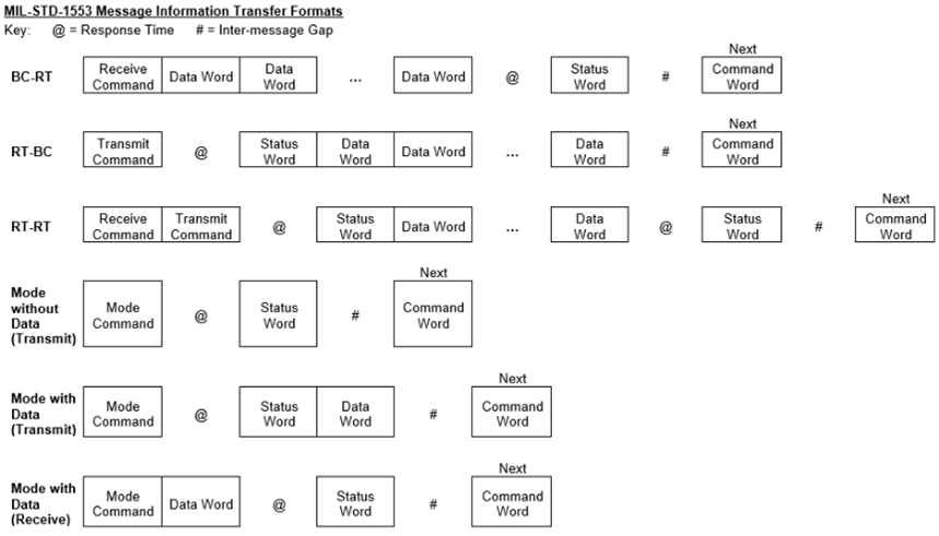
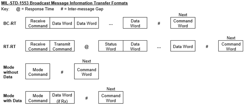
Message Components
The following are three components that make up the 1553 messages:
- Command Word
- Data Word
- Status Word
Each word type is 20 bits in length. The first 3 bits are used as a synchronization field, thereby allowing the decode clock to re-sync at the beginning of each new word. The next 16 bits are the information field. The last bit is the parity bit. Parity is based on odd parity for the single word.
Command Word
The Command Word specifies the function that the Remote Terminal is to perform.
The RT Address field states which unique remote terminal the command is intended for (no two terminals may have the same address). Note the address of 0x00 (00000b) is a valid address, and the address 0x1F (11111b) is always reserved as a broadcast address. The maximum number of terminals the data bus can support is 31.
The Transmit/Receive bit defines the direction of information flow and is always from the point of view of the Remote Terminal. A transmit command (logic 1) indicates that the Remote Terminal is to transmit data, while a receive command (logic 0) indicates that the Remote Terminal is going to receive data
The Sub-Address/Mode Code and Word Count/Mode Code fields are defined as follows:
| Sub-Address/Mode Command Field | Word Count/Mode Code Field |
| 0x00 (00000b) or 0x1F (11111b) indicates | Mode Code Command — Mode Code number to be performed |
| 0x01 (00001b) to 0x1E (11110b) indicates the Sub-Address 1 to Sub-Address 30 | Word Count — note 0x00 (00000b) is decoded as 32 data words |
Data Word
The Data Word contains the actual information that is being transferred within a message. Data Words can be transmitted by either a Remote Terminal (Transmit command) or a Bus Controller (Receive command).
Status Word
When the Remote Terminal receives a valid message, it will respond with a Status Word. The Status Word is used to convey to the Bus Controller whether a message was properly received or to convey the state of the Remote Terminal (i.e., service request, busy, etc.).
The RT Address in the Status Word should match the RT Address within the Command Word that the Remote Terminal received. With a RT-RT Transfer message, the RT address within either Status Word received (Rx or Tx), should match the RT address within the corresponding Command word sent (Rx or Tx).
| Status Bit | Description |
| Message Error (Bit 9) | This bit is set by the Remote Terminal upon detection of an error in the message or upon detection of an invalid message (i.e. Illegal Command). The error may occur in any of the Data Words within the message. When the terminal detects an error and sets this bit, none of the data received within the message is used. |
| Instrumentation (Bit 10) | This bit is always set to logic 0. |
| Service Request (Bit 11) | This bit is set to a logic 1 by the subsystem if servicing is needed. This bit is typically used when the Bus Controller is "polling" terminals to determine if they require processing. |
| Broadcast Command Received (Bit 15) | This bit indicates that the Remote Terminal received a valid broadcast command. On receiving a valid broadcast command, the Remote Terminal sets this bit to logic "1" and suppresses the transmission of its Status Word. The Bus Controller may issue a Transmit Status Word or Transmit Last Command Word Mode Code to determine if the Remote Terminal received the message properly. |
| Busy (Bit 16) | This bit indicates to the Bus Controller that the Remote Terminal is unable to move data between the Remote Terminal and the Sub-system in compliance to a command from the Bus Controller. In the earlier days of 1553, the Busy bit was required because many subsystem interfaces (analog, synchros, etc.) were much slower compared to the speed of the multiplex data bus. So instead of losing data, a terminal was able to set the Busy bit indicating to the Bus Controller to try again later. As new systems have been developed, the need for the busy bit has been reduced. |
| Subsystem Flag (Bit 17) | This bit provides "health" data regarding the subsystems to which the Remote Terminal is connected. Multiple subsystems may logically "OR" their bits together to form a composite health indicator. |
| Dynamic Bus Control Acceptance Bit (Bit 19) | This bit informs the Bus Controller that the Remote Terminal has received the Dynamic Bus Control Mode Code and has accepted control of the bus. The Remote Terminal, on transmitting its status word, becomes the Bus Controller. The Bus Controller, on receiving the status word from the Remote Terminal with this bit set, ceases to function as the Bus Controller and may become a Remote Terminal or Bus Monitor. |
| Terminal Flag (Bit 20) | This bit informs the Bus Controller of a fault or failure within the Remote Terminal. A logic "1" indicates a fault condition. |
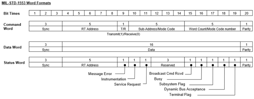
External RT Address
External discrete signals are available to support “hardwired” RT Address and configuration
External RT Address
The 1553 modules are completely software RT Address programmable and configurable. An open circuit on an address line is detected as a logic 1 and connecting the address line to ground is detected as a logic 0. The 1553 modules provided the ability to externally set the RT Address and Parity via discrete signals (CHx-RT-ADDR (0-4) and CHx- PARITY). These discrete signals are considered additional and optional based on specific application requirements. The discrete signals are single-ended and System-GND referenced.
Because of the platform (module-thru-board) available physical pin limitations, only one set of discrete signals are provided for a channel (CH) pair (channel pair 1 = CH1, CH2 and channel pair 2 = CH3, CH4). The discrete pins are provided for the odd-numbered channel, which will use these signals directly. The even channel of the channel pair will use these same pins, but the RT addressing for the even channel will be set as a “hard +1” offset from the odd-channel discrete pattern.
For example:
If the CH1 external pins are either grounded or left open to yield:
CH1-RT-ADDR0-4 pins + Parity pin = (MSB)01101(LSB) + 0 (defined as OddParity) =0xD (13d)
and the hard offset for CH2 is 1 (0x1)
then, the CH1 RT address is 0xD (13d) (wired) and the CH2 RT address will be 0xE (14d) (wired plus the hard offset).
| Discrete Signal Pin | Description (Grounding a pin = 0, leaving a pin open = 1. Unit signal pins are defaulted open = 1) |
| CHx-RT-ADDR0 thru CHx-RT-ADDR4 | Five (5) External RT address signal pins, binary bit-weighted (ADDR0=LSB); for applying a "hardwire" RT address (special applications only). MSB - (...ADDR4, ...ADDR3, ...ADDR2, ...ADDR1, ...ADDR0) - LSB |
| CHx-PARITY | Used in conjunction with external RT address signal pins. A single bit that complements the parity of CHx-RT-ADDR wire to odd parity. If the wrong parity is detected by core, only Broadcast commands would be valid for the core. If not masked, an interrupt will be generated in the event of wrong parity. |
Assisted Mode (AM)
The FTA-FTF 1553 modules have been improved to include the “Assisted Mode (AM)” feature.
In the legacy FT1-FT6 modules, the 1553 messages are fetched from the 1553 device by accessing device registers directly from the host application as shown in Figure 13. The dotted lines indicate read/write access over the bus interface. The bus interface in some cases may be relatively “slow” (ex. Ethernet interface). In this design, four bus accesses are required from the host to fetch one new 1553 message. The number of accesses increases proportionately with the number of 1553 messages to fetch from the 1553 device.
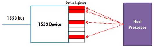
Figure 13. Legacy FT1-FT6 Message Fetch Processing
The FTA-FTF 1553 modules utilize the secondary (ARM) processor built into the module that is dedicated for the purpose of “assisting” the movement of 1553 messages from the 1553 device to the host interface. This is made possible through a system of FIFOs that carry command and response messages to and from the host CPU to a bare metal application running on the secondary processor (refer to Diagram B in Figure 14). In addition, these modules have the option of funneling all 1553 messages (per channel) to a 4k byte Message FIFO (refer to Diagram A in Figure 14) that is accessible from the host.
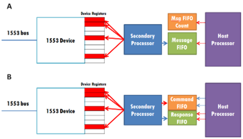
Figure 14. AM FIFO and Bus Access
In Figure 15, the dotted lines indicate slower bus read/write accesses (PCI, Ethernet) whereas the solid lines indicate fast bus accesses. When the Message FIFO is utilized (Diagram A), the Message FIFO is filled as new 1553 messages arrive. Moving the 1553 messages from the Message FIFO to the Host Processor requires 2 “slower” bus accesses to fetch all the new 1553 messages that are in the Message FIFO.
If the Message FIFO is not utilized (Diagram B only), for example to fully support DDC API compatibility, 2 writes and at least 2 reads via the “slower” bus is required to fetch one new 1553 message. The write access to the Command FIFO initiates the transfer of 1553 messages from the device to the Response FIFO and when the transfer is complete, the host can read the Response FIFO. In DDC API compatibility mode, the benefits of the “assisted” design provide significantly improved response times compared to the legacy FT module(s), especially with bulk 1553 transfers.
Figure 15 and Table 17 depict the latent time (time required for 1553 message(s) transfer from 1553 device to host memory when initiated by the host CPU) as a function of the number of 1553 messages being transferred. The three candidates for comparison are (1) Assisted Module running in Message FIFO Mode, (2) Assisted Module running in Standard Mode and (3) the Non-Assisted (Legacy) FT Module.
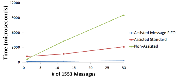
Figure 15. AM Transfer Comparisons
Table 15. Average and Worst-Case Latent Times in microseconds
| 1553 Msgs | Assisted Message FIFO | Assisted Standard | Non-Assisted | |||
| Average | Worst-Case | Average | Worst-Case | Average | Worst-Case | |
| 1 | 163.630 | 182.445 | 1169.992 | 1193.958 | 695.578 | 705.235 |
| 12 | 239.0805 | 261.298 | 1698.532 | 1735.622 | 4286.303 | 5574.973 |
| 30 | 366.4155 | 399.722 | 3179.139 | 3198.554 | 9566.732 | 9610.468 |
The benefits of this approach include:
- Reduced number of host CPU reads and writes to the device.
- Reduced host memory footprint (less application memory required on the host).
- Lower latency from 1553 bus to host memory.
Register Descriptions
The register descriptions provide the register name, Type, Data Range, Read or Write information, Initialized Value, a description of the function and, in most cases, a data table.
Assisted Mode Registers
The Assisted Mode registers are comprised of registers that support the AM Command and AM 1553 Message FIFOs.
AM Commands Registers
The registers associated with the AM Commands are divided into the following:
- Command FIFO Management (FIFO Buffer, FIFO Count, FIFO Update)
- Response FIFO Management (FIFO Buffer, FIFO Count)
The Command FIFO registers are used by the host to send commands to the AM processor to configure and operate the 1553 IP core. For every command sent from the host processor to the AM processor, the AM processor responds with a message that is sent to the host processor via the Response FIFO Buffer. The content of the response message will vary depending on the command and may contain configuration information, status information or 1553 data.
| AM Command FIFO Buffer | |
| Function: | Used to communicate with the 1553 core via the AM (secondary) processor. |
| Type: | unsigned binary word (32-bit) |
| Data Range: | 0x0000 0000 to 0xFFFF FFFF |
| Read/Write: | W |
| Initialized Value: | 0 |
| Operational Settings: | The host writes a command message to the AM Command FIFO Buffer and it is read out by the secondary processor. The secondary processor acts on the 1553 core based on the command that was read out. The AM processor will be unaware of any new command messages in the AM Command FIFO Buffer until an update is performed by writing a 1 to the AM Command FIFO Update register. |
| AM Command FIFO Count | |
| Function: | This register contains the value representing the number of 32-bit words that are currently loaded in the AM Command FIFO Buffer. |
| Type: | unsigned binary word (32-bit) |
| Data Range: | 0x0000 0000 to 0xFFFF FFFF |
| Read/Write: | R |
| Initialized Value: | 0 |
| Operational Settings: | When the host writes a command message to the AM Command FIFO Buffer, the value of the AM Command FIFO Count represents the number of 32-bit words contained in the command message. Once the message is fully read out by the AM processor, the AM Command FIFO Count goes to zero. |
| AM Command FIFO Update | |
| Function: | This register is used to update the AM Command FIFO count as it is presented to the AM processor. The purpose of this register is to ensure that the AM Command FIFO Buffer does not present incomplete command messages to the AM processor. |
| Type: | unsigned binary word (32-bit) |
| Data Range: | 0x0000 0000 to 0x0000 0001 |
| Read/Write: | W |
| Initialized Value: | 0 |
| Operational Settings: | The user should write a 1 to this register to update the AM Command FIFO count as it is seen from the AM processor. The proper way to handle sending commands to the AM processor is to write a full command message to the AM Command FIFO Buffer, then update the count by writing a 1 to the AM Command FIFO Update register. |
| AM Response FIFO Buffer | |
| Function: | Used by the AM (secondary) processor to send response messages to the host. |
| Type: | unsigned binary word (32-bit) |
| Data Range: | 0x0000 0000 to 0xFFFF FFFF |
| Read/Write: | R |
| Initialized Value: | 0 |
| Operational Settings: | After the host writes a valid command message to the AM Command FIFO Buffer and it is read out by the AM processor, the AM processor acts on the 1553 core based on the command type. Once the action is completed, the AM processor sends a response to the host processor via the AM Response FIFO Buffer. |
| AM Response FIFO Count | |
| Function: | This register contains the value that represents the number of 32-bit words that are present in the AM Response FIFO Buffer. |
| Type: | unsigned binary word (32-bit) |
| Data Range: | 0x0000 0000 to 0xFFFF FFFF |
| Read/Write: | R |
| Initialized Value: | 0 |
| Operational Settings: | When a command is sent from the host to the AM processor and it completes the commanded task, it loads the AM Response FIFO with a response message and the AM Response FIFO Count is updated with the number of 32-bit words that are contained in the response message. Once the host reads out the full response message from the AM Response FIFO Buffer, the AM Response FIFO Count will read zero. |
AM 1553 Message FIFO Registers
The Message FIFO Management registers consists of the FIFO Buffer, FIFO Count, FIFO Clear command, and the FIFO Threshold which specify threshold associated with for the “1553 Message FIFO Almost Full” status bits in the Channel Status register.
| AM 1553 Message FIFO Buffer | |
| Function: | When the channel is operating in Message FIFO mode, 1553 messages are stored in the 1553 Message FIFO Buffer. |
| Type: | unsigned binary word (32-bit) |
| Data Range: | 0x0000 0000 to 0xFFFF FFFF |
| Read/Write: | R |
| Initialized Value: | 0 |
| Operational Settings: | When the channel is configured for Message FIFO mode, new 1553 messages (comprising 1553 data words, 1553 status words, timestamp and message status information) are stored in the 1553 Message FIFO Buffer and the host can perform a block read on this register to read out a chain of 1553 messages in a single transaction. The number of 32-bit words to read out of the 1553 Message FIFO Buffer is reported in the 1553 Message FIFO Count register. Refer to Appendix - 1553 Receive Message FIFO Format to decode the single 1553 message or a chain of 1553 messages read from this buffer. |
| AM 1553 Message FIFO Count | |
| Function: | While the channel is operating in Message FIFO mode, the number of 32-bit words in the 1553 Message FIFO Buffer is reported in this register. |
| Type: | unsigned binary word (32-bit) |
| Data Range: | 0x0000 0000 to 0xFFFF FFFF |
| Read/Write: | R |
| Initialized Value: | 0 |
| Operational Settings: | When the channel is configured for Message FIFO mode, new 1553 messages (comprising 1553 data words, 1553 status words, timestamp, and message status information) are stored in the 1553 Message FIFO Buffer. The 32-bit count of a 1553 message can vary depending on the 1553 message type and 1553 data payload size. This register provides the count of 32-bit words that are currently present in the 1553 Message FIFO Buffer instead of providing the count of 1553 messages. When retrieving data from the 1553 Message FIFO Buffer, use the 1553 Message FIFO Count to obtain all 1553 messages and refer to Appendix - 1553 Receive Message FIFO Format to decode 1553 messages. |
| AM 1553 Message FIFO Clear | |
| Function: | When the channel is operating in Message FIFO mode, this register is used to clear the 1553 Message FIFO Buffer. |
| Type: | unsigned binary word (32-bit) |
| Data Range: | 0x0000 0000 to 0xFFFF FFFF |
| Read/Write: | W |
| Initialized Value: | 0 |
| Operational Settings: | Write a 1 to this register to clear the 1553 Message FIFO Buffer. Once the buffer is cleared, the 1553 Message FIFO Count register should read zero. |
| AM 1553 Message FIFO Threshold | |
| Function: | Set the "1553 Message FIFO Almost Full" status threshold value. |
| Type: | unsigned binary word (32-bit) |
| Data Range: | 1 to 1002 |
| Read/Write: | R/W |
| Initialized Value: | 512 |
| Operational Settings: | This register sets the "1553 Message FIFO Almost Full" threshold such that when the number of 32-bit words reach or surpass the threshold value, the 1553 Message FIFO Almost Full status bit will report a 1. If interrupts are enabled for this status bit, an interrupt will be generated when the number of 32-bit words reach or surpass the threshold value. |
Auxiliary Registers
| Reset | |
| Function: | A write to this register causes a reset of the channel/core. |
| Type: | unsigned binary word (32-bit) |
| Data Range: | 0x0000 0000 to 0x0000 000F |
| Read/Write: | W (Reset) |
| Initialized Value: | 0 |
| Operational Settings: | Reset — Write a 1 to reset the core. |
| D31 | D30 | D29 | D28 | D27 | D26 | D25 | D24 | D23 | D22 | D21 | D20 | D19 | D18 | D17 | D16 |
| 0 | 0 | 0 | 0 | 0 | 0 | 0 | 0 | 0 | 0 | 0 | 0 | 0 | 0 | 0 | 0 |
| D15 | D14 | D13 | D12 | D11 | D10 | D9 | D8 | D7 | D6 | D5 | D4 | D3 | D2 | D1 | D0 |
| 0 | 0 | 0 | 0 | 0 | 0 | 0 | 0 | 0 | 0 | 0 | 0 | 0 | 0 | 0 | D |
| RT Address from Backplane | |
| Function: | Provides the Remote Terminal address and the parity. |
| Type: | unsigned binary word (32-bit) |
| Data Range: | See table below. |
| Read/Write: | R |
| Initialized Value: | 0 |
| Operational Settings: | The RT values are set at the backplane and read from this register. |
| Bit | Description |
| D31:D6 | Reserved |
| D5 | RT Parity Bit: 1=Even Parity 0=Odd Parity |
| D4:D0 | RT Address of the channel. |
| D31 | D30 | D29 | D28 | D27 | D26 | D25 | D24 | D23 | D22 | D21 | D20 | D19 | D18 | D17 | D16 |
| 0 | 0 | 0 | 0 | 0 | 0 | 0 | 0 | 0 | 0 | 0 | 0 | 0 | 0 | 0 | 0 |
| D15 | D14 | D13 | D12 | D11 | D10 | D9 | D8 | D7 | D6 | D5 | D4 | D3 | D2 | D1 | D0 |
| 0 | 0 | 0 | 0 | 0 | 0 | 0 | 0 | 0 | 0 | D | D | D | D | D | D |
| Miscellaneous Bits | |
| Function: | Provides various control and configuration functions as well as status. |
| Type: | unsigned binary word (32-bit) |
| Data Range: | See table below. |
| Read/Write: | R/W |
| Initialized Value: | 0 |
| Operational Settings: | Refer to table below for definitions. |
| Bit | Description |
| D31..D16 | Reserved |
| D15 | If set, overrides external BC_DISABLE (Bus Controller Mode) with the value from bit 14 |
| D14 | BC_DISABLE override value |
| D13 | If set, overrides external M1760 hardware input (Standard) with the value from bit 12 |
| D12 | M1760 override value |
| D11 | Reserved |
| D10 | Mode value from backplane (Read Only) |
| D9 | Standard value from backplane (Read Only) Default |
| D8 | Terminate RS-422: 0=No termination 1=termination |
| D7 | Transceiver Type: 0=Sital 1=COTS (Read Only) |
| D6 | BC_DISABLE setting at the core (Read Only) |
| D5 | SSFLAG: RT Mode Only — Sets the Sub System flag (bit 2) high in the status word |
| D4 | RTAD_SW_EN: 0=No software change of RT address available 1=Enables software change of RT Address by configuration reg #6 |
| D3 | RT_ADR_LAT: 0=RT Address and parity are used as-is, Rising edge=Last RT Address and parity are sampled and stored in the core. Changes to the values are ignored 1=RT Address and parity can be latched by writing to configuration reg #5 |
| D2 | M1760 Setting at the core (Read Only) |
| D1 | Tx_inhB: 0=Enable core transmission on bus B 1=inhibit core transmission on bus B |
| D0 | Tx_inhA: 0=Enable core transmission on bus A 1=inhibit core transmission on bus A |
| D31 | D30 | D29 | D28 | D27 | D26 | D25 | D24 | D23 | D22 | D21 | D20 | D19 | D18 | D17 | D16 |
| 0 | 0 | 0 | 0 | 0 | 0 | 0 | 0 | 0 | 0 | 0 | 0 | 0 | 0 | 0 | 0 |
| D15 | D14 | D13 | D12 | D11 | D10 | D9 | D8 | D7 | D6 | D5 | D4 | D3 | D2 | D1 | D0 |
| D | D | D | D | D | D | D | D | D | D | D | D | D | D | D | D |
Status and Interrupt Registers
The registers may be set for any or all channels and will latch if a transition is detected on a channel or channels. Each channel(s) will remain latched until the channel is cleared. Multiple channels may be cleared simultaneously, if desired. Each channel bit in the register is polled for a read status. Any subsequent channel(s) transition, if detected, will propagate through to be read (rolling-latch).
Once the status register has been read, the act of writing a 1 back to the applicable status register to any specific bit (channel) location (bit mapped per channel), will “clear” the bit (set the bit to 0) if the actual interruptible event condition has cleared. If the interruptible condition “event” is still persistent while clearing, this may retrigger the interrupt.
There is a corresponding Interrupt Enable and vector associated with each “Latched” Status. Each status type may be “polled” (at any time) or is “interruptible” when interrupts are enabled and the associated Interrupt Service Routine (ISR) vectors are programmed accordingly. When programmed for “interruptible” status, interrupts are typically generated and flagged with the programmed vector available as data. The host or single board computer (SBC) typically services the interrupt by a general or specific ISR, which reads the (typically) unique programmed vector (identifier of which status generated the interrupt), reads the associated status register to determine which channel in the status register was “flagged” and then “clears” the status register. This essentially resets the interrupt mechanism, which is now ready to be triggered by the next status register detected event “flag”. “Latched Status” will trigger on either “sense on edge” or “sense on level” based on the settings of the associated Set Edge/Level Interrupt register. Sense on “edge” requires a change from low to high state to trigger the status detection, while sense on “level” is independent of the previous state. Unless otherwise specified, all status or fault indications are bit set per channel.
BIT Status
There are four registers associated with the BIT Status: Dynamic, Latched, Interrupt Enable, and Set Edge/Level Interrupt.
| BIT Status | |
| Function: | Sets the corresponding bit associated with the channel's BIT register. |
| Type: | unsigned binary word (32-bit) |
| Data Range: | 0x0000 0000 to 0x0000 000F |
| Read/Write: | R (Dynamic), R/W (Latched, Interrupt Enable, Edge/Level Interrupt) |
| Initialized Value: | 0 |
| BIT Dynamic Status | |||||||||||||||
| BIT Latched Status | |||||||||||||||
| BIT Interrupt Enable | |||||||||||||||
| BIT Set Edge/Level Interrupt | |||||||||||||||
| D31 | D30 | D29 | D28 | D27 | D26 | D25 | D24 | D23 | D22 | D21 | D20 | D19 | D18 | D17 | D16 |
| 0 | 0 | 0 | 0 | 0 | 0 | 0 | 0 | 0 | 0 | 0 | 0 | 0 | 0 | 0 | 0 |
| D15 | D14 | D13 | D12 | D11 | D10 | D9 | D8 | D7 | D6 | D5 | D4 | D3 | D2 | D1 | D0 |
| 0 | 0 | 0 | 0 | 0 | 0 | 0 | 0 | 0 | 0 | 0 | 0 | 0 | 0 | Ch2 | Ch1 |
Channel Status
There are four registers associated with the Channel Status: Dynamic, Latched, Interrupt Enable, and Set Edge/Level Interrupt. Use this register to read current or real-time status.
| Channel Status | |
| Function: | Sets the corresponding bit associated with the event type. There are separate registers for each channel. |
| Type: | unsigned binary word (32-bit) |
| Data Range: | 0 to 0x0000 001F |
| Read/Write: | R (Dynamic), R/W (Latched, Interrupt Enable, Edge/Level Interrupt) |
| Initialized Value: | N/A |
| Channel Dynamic Status | |||||||||||||||
| Channel Latched Status | |||||||||||||||
| Channel Interrupt Enable | |||||||||||||||
| Channel Set Edge/Level Interrupt | |||||||||||||||
| D31 | D30 | D29 | D28 | D27 | D26 | D25 | D24 | D23 | D22 | D21 | D20 | D19 | D18 | D17 | D16 |
| 0 | 0 | 0 | 0 | 0 | 0 | 0 | 0 | 0 | 0 | 0 | 0 | 0 | 0 | 0 | 0 |
| D15 | D14 | D13 | D12 | D11 | D10 | D9 | D8 | D7 | D6 | D5 | D4 | D3 | D2 | D1 | D0 |
| 0 | 0 | 0 | 0 | 0 | 0 | 0 | 0 | 0 | 0 | 0 | 0 | D | D | D | D |
| Bit | Description | Notes |
| D0 | 1553 Core Interrupt | An interrupt has been signaled from the 1553 core. The specific interrupt signaling event(s) can be identified by reading the core status registers. |
| D1 | 1553 Message FIFO Full | The 1553 Message FIFO is full and will not store any additional messages until messages are read out or the FIFO is cleared. |
| D2 | 1553 Message FIFO Almost Full | The 1553 Message FIFO is almost full. The almost full threshold may be set by writing a value between 1 and 1002 to the Message FIFO Almost Full Threshold register. |
| D3 | 1553 Message FIFO Empty | The 1553 Message FIFO does not contain any messages. |
| D4 | 1553 Message FIFO Rx Available | The 1553 Message FIFO contains one or more messages. |
| D31:D5 | Reserved |
Function Register Map
| Configuration/Control |
| Status |
| AM COMMANDS REGISTERS | |||||
| OFFSET | REGISTER NAME | ACCESS | OFFSET | REGISTER NAME | ACCESS |
| 0x10B0 | AM Command FIFO Buffer Ch 1 | W | 0x10B4 | AM Command FIFO Count Ch 1 | R |
| 0x18B0 | AM Command FIFO Buffer Ch 2 | W | 0x18B4 | AM Command FIFO Count Ch 2 | R |
| 0x10B8 | AM Command FIFO Update Ch 1 | W | |||
| 0x18B8 | AM Command FIFO Update Ch 2 | W | |||
| 0x10C0 | AM Response FIFO Buffer Ch 1 | R | 0x10C4 | AM Response FIFO Count Ch 1 | R |
| 0x18C0 | AM Response FIFO Buffer Ch 2 | R | 0x18C4 | AM Response FIFO Count Ch 2 | R |
| AM 1553 MESSAGE FIFO REGISTERS | |||||
| OFFSET | REGISTER NAME | ACCESS | OFFSET | REGISTER NAME | ACCESS |
| 0x10D0 | AM 1553 Message FIFO Buffer Ch 1 | R | 0x10D4 | AM Message FIFO Count Ch 1 | R |
| 0x18D0 | AM 1553 Message FIFO Buffer Ch 2 | R | 0x18D4 | AM Message FIFO Count Ch 2 | R |
| 0x10D8 | AM Message FIFO Clear Ch 1 | W | 0x10DC | AM Message FIFO Threshold Ch 1 | R/W |
| 0x18D8 | AM Message FIFO Clear Ch 2 | W | 0x18DC | AM Message FIFO Threshold Ch 2 | R/W |
| AUXILIARY REGISTERS | |||||
| OFFSET | REGISTER NAME | ACCESS | OFFSET | REGISTER NAME | ACCESS |
| 0x1080 | RT Address from Backplane Ch 1 | R | 0x1080 | Reset Ch 1 | W |
| 0x1880 | RT Address from Backplane Ch 2 | R | 0x1880 | Reset Ch 2 | W |
| 0x1084 | Miscellaneous Bits Ch 1 | R/W | |||
| 0x1884 | Miscellaneous Bits Ch 2 | R/W | |||
| BIT STATUS REGISTERS | |||||
| *When an event is detected, the bit associated with the event is set in this register and will remain set until the user clears the event bit. Clearing the bit requires writing a 1 back to the specific bit that was set when read (i.e., write-1-to-clear, writing a “1” to a bit set to “1” will set the bit to “0). | |||||
| OFFSET | REGISTER NAME | ACCESS | OFFSET | REGISTER NAME | ACCESS |
| 0x0800 | Dynamic Status | R | |||
| 0x0804 | Latched Status* | R/W | |||
| 0x0808 | Interrupt Enable | R/W | |||
| 0x080C | Set Edge/Level Interrupt | R/W | |||
| 1553 CHANNEL STATUS REGISTERS | |||||
| *When an event is detected, the bit associated with the event is set in this register and will remain set until the user clears the event bit. Clearing the bit requires writing a 1 back to the specific bit that was set when read (i.e., write-1-to-clear, writing a “1” to a bit set to “1” will set the bit to “0”). | |||||
| OFFSET | REGISTER NAME | ACCESS | OFFSET | REGISTER NAME | ACCESS |
| 0x0810 | Channel Dynamic Status Ch 1 | R | 0x0820 | Channel Dynamic Status Ch 2 | R |
| 0x0814 | Channel Latched Status Ch 1* | R/W | 0x0824 | Channel Latched Status Ch 2* | R/W |
| 0x0818 | Channel Interrupt Enable Ch 1 | R/W | 0x0828 | Channel Interrupt Enable Ch 2 | R/W |
| 0x081C | Channel Set Edge/Level Interrupt Ch 1 | R/W | 0x082C | Channel Set Edge/Level Interrupt Ch 2 | R/W |
Appendix: 1553 Receive Message FIFO Format
General Rx FIFO 1553 Header Format
| Message Type | Index | High Word (16-bits) | Low Word (16-bits) |
| General Rx FIFO 1553 Header | 0 | Msg Type (Upper 8 bits) Msg Size (Lower 8 bits - number of 16-bit words) | Padding (0x15F3) |
| 1 | Time Tag | Block Status | |
| 2 | Depends on Msg Type | Command Word |
BC
| Message Type | Index | High Word (16-bits) | Low Word (16-bits) |
| BC to RT Message | 0 | 0x0006 | Padding (0x15F3) |
| 1 | Time Tag | Block Status | |
| 2 | RT Status | Command Word | |
| RT to BC Message | 0 | 0x01XX | Padding (0x15F3) |
| 1 | Time Tag | Block Status | |
| 2 | RT Status | Command Word | |
| 3 | Second 16-bit 1553 Data Word | First 16-bit 1553 Data Word | |
| ... | ... | ... | |
| N | ... | ... | |
| RT to RT Message | 0 | 0x0208 | Padding (0x15F3) |
| 1 | Time Tag | Block Status | |
| 2 | RT Status 1 | Command Word 1 | |
| 3 | RT Status 2 | Command Word 2 | |
| Mode Code Message No Data | 0 | 0x0506 | Padding (0x15F3) |
| 1 | Time Tag | Block Status | |
| 2 | RT Status | Command Word | |
| Mode Code Message with Data Rx | 0 | 0x0606 | Padding (0x15F3) |
| 1 | Time Tag | Block Status | |
| 2 | RT Status | Command Word | |
| Mode Code Message with Data Tx | 0 | 0x0707 | Padding (0x15F3) |
| 1 | Time Tag | Block Status | |
| 2 | RT Status | Command Word | |
| 3 | 0x0000 | 1553 Data Word | |
| Broadcast Message | 0 | 0x0805 | Padding (0x15F3) |
| 1 | Time Tag | Block Status | |
| 2 | 0x0000 | Command Word | |
| Broadcast Message RT to RT | 0 | 0x0A07 | Padding (0x15F3) |
| 1 | Time Tag | Block Status | |
| 2 | RT Status | Command Word 1 | |
| 3 | 0x0000 | Command Word 2 | |
| Broadcast Mode Message with No Data | 0 | 0x0D05 | Padding (0x15F3) |
| 1 | Time Tag | Block Status | |
| 2 | 0x0000 | Command Word | |
| Broadcast Mode Message with Data | 0 | 0x0E05 | Padding (0x15F3) |
| 1 | Time Tag | Block Status | |
| 2 | 0x0000 | Command Word |
RT
| Message Type | Index | High Word (16-bits) | Low Word (16-bits) |
| BC to RT Message | 0 | 0x00XX | Padding (0x15F3) |
| 1 | Time Tag | Block Status | |
| 2 | RT Status | Command Word | |
| 3 | Second 16-bit 1553 Data Word | First 16-bit 1553 Data Word | |
| ... | ... | ... | |
| N | ... | ... | |
| RT to BC Message | 0 | 0x0106 | Padding (0x15F3) |
| 1 | Time Tag | Block Status | |
| 2 | RT Status | Command Word | |
| RT to RT Message | 0 | 0x02XX | Padding (0x15F3) |
| 1 | Time Tag | Block Status | |
| 2 | RT Status 1 | Command Word 1 | |
| 3 | RT Status 2 | Command Word 2 | |
| 4 | Second 16-bit 1553 Data Word | First 16-bit 1553 Data Word | |
| ... | ... | ... | |
| N | ... | ... | |
| Mode Code Message No Data | 0 | 0x0506 | Padding (0x15F3) |
| 1 | Time Tag | Block Status | |
| 2 | RT Status | Command Word | |
| Mode Code Message with Data Rx | 0 | 0x0607 | Padding (0x15F3) |
| 1 | Time Tag | Block Status | |
| 2 | RT Status | Command Word | |
| 3 | 0x0000 | 1553 Data Word | |
| Mode Code Message with Data Tx | 0 | 0x0706 | Padding (0x15F3) |
| 1 | Time Tag | Block Status | |
| 2 | RT Status | Command Word | |
| Broadcast Message | 0 | 0x08XX | Padding (0x15F3) |
| 1 | Time Tag | Block Status | |
| 2 | First 16-bit 1553 Data Word | Command Word | |
| 3 | Third 16-bit 1553 Data Word | Second 16-bit 1553 Data Word | |
| ... | ... | ... | |
| N | ... | ... | |
| Broadcast Message RT to RT | 0 | 0x0AXX | Padding (0x15F3) |
| 1 | Time Tag | Block Status | |
| 2 | RT Status 1 | Command Word 1 | |
| 3 | First 16-bit 1553 Data Word | Command Word 2 | |
| 4 | Third 16-bit 1553 Data Word | Second 16-bit 1553 Data Word | |
| ... | ... | ... | |
| N | ... | ... | |
| Broadcast Mode Message with No Data | 0 | 0x0D05 | Padding (0x15F3) |
| 1 | Time Tag | Block Status | |
| 2 | 0x0000 | Command Word | |
| Broadcast Mode Message with Data | 0 | 0x0E06 | Padding (0x15F3) |
| 1 | Time Tag | Block Status | |
| 2 | 1553 Data Word | Command Word |
MT
| Message Type | Index | High Word (16-bits) | Low Word (16-bits) |
| BC to RT Message | 0 | 0x00XX | Padding (0x15F3) |
| 1 | Time Tag | Block Status | |
| 2 | RT Status | Command Word | |
| 3 | Second 16-bit 1553 Data Word | First 16-bit 1553 Data Word | |
| ... | ... | ... | |
| N | ... | ... | |
| RT to BC Message | 0 | 0x01XX | Padding (0x15F3) |
| 1 | Time Tag | Block Status | |
| 2 | RT Status | Command Word | |
| 3 | Second 16-bit 1553 Data Word | First 16-bit 1553 Data Word | |
| ... | ... | ... | |
| N | ... | ... | |
| RT to RT Message | 0 | 0x02XX | Padding (0x15F3) |
| 1 | Time Tag | Block Status | |
| 2 | RT Status 1 | Command Word 1 | |
| 3 | RT Status 2 | Command Word 2 | |
| 4 | Second 16-bit 1553 Data Word | First 16-bit 1553 Data Word | |
| ... | ... | ... | |
| N | ... | ... | |
| Mode Code Message No Data | 0 | 0x0506 | Padding (0x15F3) |
| 1 | Time Tag | Block Status | |
| 2 | RT Status | Command Word | |
| Mode Code Message with Data Rx | 0 | 0x0607 | Padding (0x15F3) |
| 1 | Time Tag | Block Status | |
| 2 | RT Status | Command Word | |
| 3 | 0x0000 | 1553 Data Word | |
| Mode Code Message with Data Tx | 0 | 0x0706 | Padding (0x15F3) |
| 1 | Time Tag | Block Status | |
| 2 | RT Status | Command Word | |
| Broadcast Message | 0 | 0x08XX | Padding (0x15F3) |
| 1 | Time Tag | Block Status | |
| 2 | First 16-bit 1553 Data Word | Command Word | |
| 3 | Third 16-bit 1553 Data Word | Second 16-bit 1553 Data Word | |
| ... | ... | ... | |
| N | ... | ... | |
| Broadcast Message RT to RT | 0 | 0x0AXX | Padding (0x15F3) |
| 1 | Time Tag | Block Status | |
| 2 | RT Status 1 | Command Word 1 | |
| 3 | First 16-bit 1553 Data Word | Command Word 2 | |
| 4 | Third 16-bit 1553 Data Word | Second 16-bit 1553 Data Word | |
| ... | ... | ... | |
| N | ... | ... | |
| Broadcast Mode Message with No Data | 0 | 0x0D05 | Padding (0x15F3) |
| 1 | Time Tag | Block Status | |
| 2 | 0x0000 | Command Word | |
| Broadcast Mode Message with Data | 0 | 0x0E06 | Padding (0x15F3) |
| 1 | Time Tag | Block Status | |
| 2 | 1553 Data Word | Command Word |
ARINC 429/575 Function
Principle of Operation
Through a CM5 combination module, the onboard ARINC 429/575 communications function provides up to 8 programmable ARINC-429 channels (AR1 module-type). Each channel is software selectable for transmit and/or receive, high or low speed, and odd or no parity. Therefore, AR1 can support multiple ARINC 429 and 575 channels simultaneously.
Receive Operation
Serial BRZ data is decoded for logic states: one, zero or null. Once Word Gap is detected (4 null states) the receiver waits for either a zero or one state to start the serial-to-parallel shift function. If a waveform timing fault is detected before the serial/parallel function is complete, operation is terminated, and the receiver returns to waiting for Word Gap detection. The serial-to-parallel output data is validated for odd parity, Label and Serial-to-Digital Interface (SDI).
If message validation (filtering) is enabled, the module compares the SDI/Label of incoming ARINC messages to a list of desired SDI/Labels in validation (match) memory and only stores messages with an SDI/Label in the list. The message is stored in the receive FIFO or mailbox, depending if the channel is in FIFO receive mode or mailbox receive mode. In FIFO Receive Mode, received ARINC messages / words are stored with an associated status word and an optional time-stamp value in the channel’s receive FIFO. Additionally, the Rx FIFO can be set for either bounded or circular mode, which determines FIFO behavior when it is full. In bounded mode, newly received ARINC messages are discarded if the FIFO is full whereas in circular mode, new ARINC messages overwrite the oldest messages in the FIFO. In mailbox mode, received ARINC words are stored in mailboxes or records in RAM that are indexed by the SDI/Label of the ARINC word. Each mailbox contains a status word associated with the message, the ARINC message / word, and an optional 32-bit timestamp value. The status word indicates parity error and new message status.
Transmit Operation
Transmitters are tri-stated when TX is not enabled. Transmit operates in one of three modes: Immediate FIFO, Triggered FIFO, and Scheduled. In immediate mode, ARINC data is sent as soon as data is written to the transmit FIFO. In Triggered FIFO mode, a write to the Transmit Trigger register is needed to start transmission of the transmit FIFO contents. Transmission continues until the FIFO is empty. To transmit more data after the FIFO empties out, issue a new trigger after filling the transmit FIFO with new data.
For either FIFO mode, a transmit FIFO Rate register is provided to control rate of transmission. The contents of this register specify the gap time between transmitted words from the FIFO. The default is the minimum ARINC gap time of 4-bit times.
Schedule mode transmits ARINC data words according to a prebuilt schedule table in Transmit Schedule RAM. In the Schedule table, various commands define what messages are sent and the duration of gaps between each message. Note that a Gap (Gap or Fixed Gap) command must be explicitly added in between each Message command otherwise a gap will not be inserted between messages. The ARINC data words and gap times are stored in the Transmit Message RAM and can be updated on the fly as the schedule executes. A write to the Transmit Trigger register initiates the schedule and commands are executed starting from the first command (address 0x0) in the Schedule RAM. While a schedule is running, an ARINC word can be transmitted asynchronously by writing the async data word to the Async Transmit Data register. After it has transmitted, the Async Data Available bit will be cleared from the Channel Status register and the Async Data Sent Interrupt will be set if enabled. The Async Data Available bit in Channel Status also gets cleared by a Stop Cmd in a schedule or if a Transmit Stop command is issued from the Transmit Stop register. Use the Fixed Gap command instead of the Gap command to disable async transmissions during the schedule gap time. Gap and Fixed Gap commands can both be used when building the transmit schedule.
Schedule Transmit Commands
ARINC 429/575 scheduling is controlled by commands that are written to the Transmit Schedule RAM. The available commands are:
| Command Name | Description |
| Message | This command takes a parameter that specifies the location in Transmit Message memory containing the ARINC data word to be sent. The word is transmitted when the Message command is executed. This ARINC word can be modified in Tx Message memory while the schedule is running. |
| Gap | This command takes a parameter that specifies the location in Transmit Message memory containing a 20-bit gap time value. Values less than 4 are invalid. If the previous command was a Message, then that message is transmitted and then the transmitter waits out the specified gap time transmitting nulls. An exception to this is if there is an async data word available. If the gap time is greater or equal to 40-bit times (4-bit gap time plus one ARINC word plus another 4-bit gap time) an async data word, if available, will be transmitted during this time. If a new async data word is made available and the remaining gap time is large enough to accommodate another async data word transmission, then the new async data word will be transmitted after a 4-bit gap time. Multiple async data word transmissions can thus occur if the remaining gap time is large enough to accommodate a message and the required minimum 4-bit gap time. Otherwise, the transmitter waits out the remaining gap time before executing the next command. |
| Fixed Gap | This command takes a parameter that specifies the location in Transmit Message memory containing a 20-bit gap time value. Values less than 4 are invalid. If the previous command was a Message, then that message is transmitted with the specified gap time appended. If the previous command was not a Message, then the transmitter waits for the specified gap time before executing the next command. The difference between the Fixed Gap and Gap command is that Fixed Gap will prevent the transmission of async data words during the gap time. Use Fixed Gap to only allow nulls to be transmitted during the gap time. |
| Pause | This command causes the transmitter to pause execution of the schedule after transmitting the current word. Either a Transmit Trigger command is issued to resume execution, or a Transmit Stop command is issued to halt execution. |
| Interrupt | This command causes the Schedule Interrupt to be set if Schedule Interrupt is enabled. An unlatched version of this flag is also visible in the channel status register. |
| Jump | Jumps to the 9-bit address in Schedule memory pointed to by this command and resumes execution there. |
| Stop | This command causes the transmitter to stop execution of the schedule after transmitting the current word. |
ARINC 429/575 Built-in Test
The AR1 module supports three types of built-in tests: Power-On, Continuous Background and Initiated. The results of these tests are logically ORed together and stored in the BIT Dynamic Status and BIT Latched Status registers.
Power-On Self-Test (POST) / Power-on BIT (PBIT) / Start-up BIT(SBIT)
The power-on self-test is performed on each channel automatically when power is applied and reports the results in the BIT Status register when complete. After power-on, the Power-on BIT Complete register should be checked to ensure that POST/PBIT/SBIT test is complete before reading the BIT Dynamic Status and BIT Latched Status registers.
Continuous Background Built-In Test
The background Built-In-Test or Continuous BIT (CBIT) runs in the background for each enabled channel. In Transmit operations, internal transmit data is compared to loop-back data received by the ARINC receivers. When the channel is configured for Receive operation, receive data is continuously monitored via a secondary parallel path circuit and compared to the primary input receive data. If the data does not match, the technique used by the automatic background BIT test consists of an “add-2, subtract-1” counting scheme. The BIT counter is incremented by 2 when a BIT-fault is detected and decremented by 1 when there is no BIT fault detected and the BIT counter is greater than 0. When the BIT counter exceeds the (programmed) Background BIT Threshold value, the specific channel’s fault bit in the BIT status register will be set. The “add-2, subtract-1” counting scheme effectively filters momentary or intermittent anomalies by allowing them to “come and go“ before a BIT fault status or indication is flagged (e.g. BIT faults would register when sustained). This prevents spurious faults from registering valid such as those caused by EMI and/or dirty power causing false BIT faults. Putting more “weight” on errors (“add-2”) and less “weight” on subsequent passing results (subtract-1) will result in a BIT failure indication even if a channel “oscillates” between a pass and fail state. Results of the Continuous BIT are stored in the BIT Dynamic Status and BIT Latched Status register.
Initiated Built-In Test
The Initiated Built-In-Test (IBIT) is an internal loopback available for each channel of the AR1 module. The test is initiated by setting the bit for the associated channel in the Test Enabled register to a 1. Once enabled, they must wait at least 3 msec before checking to see if the bit for the associated channel in the Test Enabled register reads a 0. When the AR1 clears the bit, it means that the test has completed, and its results can be checked. The results of the IBIT is stored in the BIT Dynamic Status and BIT Latched Status registers, a 0 indicates that the channel has passed and a 1 indicates that it failed.
Loop-Back Operation
Transmit and receive operation of an AR1 channel can be verified internally by enabling both Tx and Rx on the same channel. Tx Scheduling is not supported when the channel is placed in this mode.
Transient Protection
The module is normally configured for transient protection but can be specified without if protection is implemented externally.
Status and Interrupts The AR1 Module provide registers that indicate faults or events. Refer to ‘Appendix B: Status and Interrupts’ for the Principle of Operation description.
Register Descriptions
The register descriptions provide the register name, Type, Data Range, Read or Write information, Initialized Value, a description of the function and, in most cases, a data table.
Receive Registers
The registers listed are associated with data that is received on the AR1 channels. Two modes of message storage are supported: Receive FIFO and Receive Mailbox.
Receive FIFO Mode Registers
The Receive FIFO Mode Registers contain information about ARINC messages that are received via the Receive FIFO buffer on the AR1 channel. The registers associated with this feature are:
- Receive FIFO Message Buffer
- Receive FIFO Message Count
- Receive FIFO Almost Full Threshold
- Receive FIFO Size
Receive FIFO Message Buffer
| Receive FIFO Message Buffer | |
| Function: | In FIFO receive mode, the received ARINC messages are stored in this buffer. |
| Type: | unsigned binary word (32-bit) |
| Data Range: | 0 to 0xFFFF FFFF |
| Read/Write: | R |
| Initialized Value: | N/A |
| Operational Settings: | Perform two reads from this register to retrieve the Status word and the ARINC data word, respectively. If Time Stamping is enabled, perform one more read to retrieve the timestamp. |
| Message Status Word | |||||||||||||||
| D31 | D30 | D29 | D28 | D27 | D26 | D25 | D24 | D23 | D22 | D21 | D20 | D19 | D18 | D17 | D16 |
| 0 | 0 | 0 | 0 | 0 | 0 | 0 | 0 | 0 | 0 | 0 | 0 | 0 | 0 | 0 | 0 |
| D15 | D14 | D13 | D12 | D11 | D10 | D9 | D8 | D7 | D6 | D5 | D4 | D3 | D2 | D1 | D0 |
| 0 | 0 | 0 | 0 | 0 | 0 | 0 | 0 | 0 | 0 | 0 | 0 | 0 | 0 | N | PE |
| Data Word | |||||||||||||||
| D31 | D30 | D29 | D28 | D27 | D26 | D25 | D24 | D23 | D22 | D21 | D20 | D19 | D18 | D17 | D16 |
| D | D | D | D | D | D | D | D | D | D | D | D | D | D | D | D |
| D15 | D14 | D13 | D12 | D11 | D10 | D9 | D8 | D7 | D6 | D5 | D4 | D3 | D2 | D1 | D0 |
| D | D | D | D | D | D | D | D | D | D | D | D | D | D | D | D |
| Timestamp Word (*if enabled) | |||||||||||||||
| D31 | D30 | D29 | D28 | D27 | D26 | D25 | D24 | D23 | D22 | D21 | D20 | D19 | D18 | D17 | D16 |
| D | D | D | D | D | D | D | D | D | D | D | D | D | D | D | D |
| D15 | D14 | D13 | D12 | D11 | D10 | D9 | D8 | D7 | D6 | D5 | D4 | D3 | D2 | D1 | D0 |
| D | D | D | D | D | D | D | D | D | D | D | D | D | D | D | D |
| Symbol | Description |
| PE = Parity Error | 1 Calculated parity does not match the received parity bit |
| N = New message | 1 Message has not been read yet |
| Receive FIFO Message Count | |
| Function: | Contains the number of ARINC messages in the receive FIFO in Receive FIFO mode. |
| Type: | unsigned binary word (32-bit) |
| Data Range: | 0 to 255 |
| Read/Write: | R |
| Initialized Value: | 0 |
| Operational Settings: | A received message consists of the message status word and the ARINC data word. If time stamping is enabled, a 32-bit timestamp is also included in the message. For example, if this register reads 1, indicating one message is loaded in the receive FIFO, perform two reads from the Receive FIFO Message Buffer register to retrieve the full message (status word and ARINC data word) if time stamping is disabled, or perform three reads to retrieve the full message (status word, ARINC data word and timestamp word) if time stamping is enabled. |
| D31 | D30 | D29 | D28 | D27 | D26 | D25 | D24 | D23 | D22 | D21 | D20 | D19 | D18 | D17 | D16 |
| 0 | 0 | 0 | 0 | 0 | 0 | 0 | 0 | 0 | 0 | 0 | 0 | 0 | 0 | 0 | 0 |
| D15 | D14 | D13 | D12 | D11 | D10 | D9 | D8 | D7 | D6 | D5 | D4 | D3 | D2 | D1 | D0 |
| 0 | 0 | 0 | 0 | 0 | 0 | 0 | 0 | D | D | D | D | D | D | D | D |
| Receive FIFO Almost Full Threshold | |
| Function: | Specifies the level of the receive FIFO buffer, equal or above, at which the Rx FIFO Almost Full Status bit D1 in the Channel Status register is flagged (High True). |
| Type: | unsigned binary word (32-bit) |
| Data Range: | 0 to 255 |
| Read/Write: | R/W |
| Initialized Value: | 128 (0x0080) |
| Operational Settings: | If the Interrupt Enable register interrupt is enabled, a SYSTEM interrupt will be generated when the receive FIFO level increases and reaches the threshold level. This register does NOT get reset by a channel reset. |
| D31 | D30 | D29 | D28 | D27 | D26 | D25 | D24 | D23 | D22 | D21 | D20 | D19 | D18 | D17 | D16 |
| 0 | 0 | 0 | 0 | 0 | 0 | 0 | 0 | 0 | 0 | 0 | 0 | 0 | 0 | 0 | 0 |
| D15 | D14 | D13 | D12 | D11 | D10 | D9 | D8 | D7 | D6 | D5 | D4 | D3 | D2 | D1 | D0 |
| 0 | 0 | 0 | 0 | 0 | 0 | 0 | 0 | D | D | D | D | D | D | D | D |
| Receive FIFO Size | |
| Function: | Specifies the size of the Rx FIFO buffer. The default size is 255 messages. |
| Type: | unsigned binary word (32-bit) |
| Data Range: | 1 to 255 |
| Read/Write: | R/W |
| Initialized Value: | 255 (0xFF) |
| Operational Settings: | This setting affects the Rx FIFO size when the Rx FIFO is configured in either Rx FIFO Bounded or Circular mode. |
| D31 | D30 | D29 | D28 | D27 | D26 | D25 | D24 | D23 | D22 | D21 | D20 | D19 | D18 | D17 | D16 |
| 0 | 0 | 0 | 0 | 0 | 0 | 0 | 0 | 0 | 0 | 0 | 0 | 0 | 0 | 0 | 0 |
| D15 | D14 | D13 | D12 | D11 | D10 | D9 | D8 | D7 | D6 | D5 | D4 | D3 | D2 | D1 | D0 |
| 0 | 0 | 0 | 0 | 0 | 0 | 0 | 0 | D | D | D | D | D | D | D | D |
Receive Mailbox Mode Registers
The Receive Mailbox Mode Registers contain information about ARINC messages that are received via mailboxes on the AR1 channel. The registers associated with this feature are:
- Receive FIFO SDI/Label Buffer
- Receive FIFO SDI/Label Count
- Receive FIFO Almost Full Threshold
- Receive FIFO Size
- Mailbox Status Data
- Mailbox Message Data
- Mailbox Timestamp Data
- Receive FIFO SDI/Label Buffer
| Receive FIFO SDI/Label Buffer | |
| Function: | In Mailbox receive mode, SDI/Label of received messages are stored in this buffer. |
| Type: | unsigned binary word (32-bit) |
| Data Range: | 0 to 0x0000 03FF |
| Read/Write: | R |
| Initialized Value: | N/A |
| Operational Settings: | In Mailbox receive mode, this FIFO contains the 10-bit SDI/Label of newly received messages. This provides a list to the user showing which mailboxes contain new messages since the last time this FIFO was read. |
| D31 | D30 | D29 | D28 | D27 | D26 | D25 | D24 | D23 | D22 | D21 | D20 | D19 | D18 | D17 | D16 |
| 0 | 0 | 0 | 0 | 0 | 0 | 0 | 0 | 0 | 0 | 0 | 0 | 0 | 0 | 0 | 0 |
| D15 | D14 | D13 | D12 | D11 | D10 | D9 | D8 | D7 | D6 | D5 | D4 | D3 | D2 | D1 | D0 |
| 0 | 0 | 0 | 0 | 0 | 0 | A10 | A9 | A8 | A7 | A6 | A5 | A4 | A3 | A2 | A1 |
| Symbol | Description |
| A8–A1 | Label (A8 is MSB and A1 is LSB) |
| A10–A9 | SDI |
| Receive FIFO SDI/Label Count | |
| Function: | Contains the number of newly received SDI/Labels in the receive FIFO in Receive Mailbox mode. |
| Type: | unsigned binary word (32-bit) |
| Data Range: | 0 to 255 |
| Read/Write: | R |
| Initialized Value: | 0 |
| Operational Settings: | In Mailbox receive mode, this register contains the number of newly received SDI/Labels in the receive FIFO. The user may perform this number of reads on the Receive FIFO SDI/Label Buffer register to retrieve all SDI/Labels. |
| D31 | D30 | D29 | D28 | D27 | D26 | D25 | D24 | D23 | D22 | D21 | D20 | D19 | D18 | D17 | D16 |
| 0 | 0 | 0 | 0 | 0 | 0 | 0 | 0 | 0 | 0 | 0 | 0 | 0 | 0 | 0 | 0 |
| D15 | D14 | D13 | D12 | D11 | D10 | D9 | D8 | D7 | D6 | D5 | D4 | D3 | D2 | D1 | D0 |
| 0 | 0 | 0 | 0 | 0 | 0 | 0 | 0 | D | D | D | D | D | D | D | D |
| Receive FIFO Almost Full Threshold | |
| Function: | Specifies the level of the receive FIFO buffer, equal or above, at which the Rx FIFO Almost Full Status bit D1 in the Channel Status register, is flagged (High True). |
| Type: | unsigned binary word (32-bit) |
| Range: | 0 to 255 |
| Read/Write: | R/W |
| Initialized Value: | 128 (0x0080) |
| Operational Settings: | If the Interrupt Enable register interrupt is enabled, a SYSTEM interrupt will be generated when the receive FIFO level increases and reaches the threshold level. This register does NOT get reset by a channel reset. |
| D31 | D30 | D29 | D28 | D27 | D26 | D25 | D24 | D23 | D22 | D21 | D20 | D19 | D18 | D17 | D16 |
| 0 | 0 | 0 | 0 | 0 | 0 | 0 | 0 | 0 | 0 | 0 | 0 | 0 | 0 | 0 | 0 |
| D15 | D14 | D13 | D12 | D11 | D10 | D9 | D8 | D7 | D6 | D5 | D4 | D3 | D2 | D1 | D0 |
| 0 | 0 | 0 | 0 | 0 | 0 | 0 | 0 | D | D | D | D | D | D | D | D |
| Receive FIFO Size | |
| Function: | Specifies the size of the Rx FIFO buffer. The default size is 255 SDI/Labels. |
| Type: | unsigned binary word (32-bit) |
| Range: | 1 to 255 |
| Read/Write: | R/W |
| Initialized Value: | 255 (0xFF) |
| Operational Settings: | This setting affects the Rx FIFO size when the Rx FIFO is configured in either Rx FIFO Bounded or Circular mode. |
| D31 | D30 | D29 | D28 | D27 | D26 | D25 | D24 | D23 | D22 | D21 | D20 | D19 | D18 | D17 | D16 |
| 0 | 0 | 0 | 0 | 0 | 0 | 0 | 0 | 0 | 0 | 0 | 0 | 0 | 0 | 0 | 0 |
| D15 | D14 | D13 | D12 | D11 | D10 | D9 | D8 | D7 | D6 | D5 | D4 | D3 | D2 | D1 | D0 |
| 0 | 0 | 0 | 0 | 0 | 0 | 0 | 0 | D | D | D | D | D | D | D | D |
| Mailbox Status Data | |
| Function: | Stores ARINC Status data word. |
| Type: | unsigned binary word (32-bit) |
| Data Range: | 0 to 0x0000 0003 |
| Read/Write: | R |
| Initialized Value: | 0 |
| Operational Settings: | This is a 32-bit value that contains status information associated with the received ARINC word. D1 of 1 indicates that the received ARINC word is a new message. D0 of 1 indicates a parity error is present in the ARINC message. There are 1024 Mailbox Status Data registers, one for each SDI/Label. The user can determine which Mailbox Status Data registers contain new data based on newly received SDI/Labels in the receive FIFO. |
| D31 | D30 | D29 | D28 | D27 | D26 | D25 | D24 | D23 | D22 | D21 | D20 | D19 | D18 | D17 | D16 |
| 0 | 0 | 0 | 0 | 0 | 0 | 0 | 0 | 0 | 0 | 0 | 0 | 0 | 0 | 0 | 0 |
| D15 | D14 | D13 | D12 | D11 | D10 | D9 | D8 | D7 | D6 | D5 | D4 | D3 | D2 | D1 | D0 |
| 0 | 0 | 0 | 0 | 0 | 0 | 0 | 0 | 0 | 0 | 0 | 0 | 0 | 0 | N | PE |
| Symbol | Description |
| PE = Parity Error | 1 Calculated parity does not match the received parity bit |
| N = New message | 1 This is a new ARINC message |
| Mailbox Message Data | |
| Function: | Stores ARINC Message data word. |
| Type: | unsigned binary word (32-bit) |
| Data Range: | 0 to 0xFFFF FFFF |
| Read/Write: | R |
| Initialized Value: | 0 |
| Operational Settings: | This is the 32-bit ARINC data word. There are 1024 Mailbox Message Data registers, one for each SDI/Label. The user can determine which Mailbox Message Data registers contain new data based on newly received SDI/Labels in the receive FIFO. |
| Mailbox Timestamp Data | |
| Function: | Stores ARINC Timestamp data word. |
| Type: | unsigned binary word (32-bit) |
| Data Range: | 0 to 0xFFFF FFFF |
| Read/Write: | R |
| Initialized Value: | 0 |
| Operational Settings: | This is the 32-bit timestamp associated with the received ARINC word. There are 1024 Mailbox Timestamp Data registers, one for each SDI/Label. The user can determine which Mailbox Timestamp Data registers contain new data based on newly received SDI/Labels in the receive FIFO. |
Timestamp Registers
| Timestamp Control | |
| Function: | Determines the resolution of the timestamp counter. |
| Type: | unsigned binary word (32-bit) |
| Data Range: | 0 to 0x0000 0007 |
| Read/Write: | R/W |
| Initialized Value: | 0 (1 µsec) |
| Operational Settings: | The LSB can have one of four time values. Set bit D2 to zero out the timestamp counter. |
| D31 | D30 | D29 | D28 | D27 | D26 | D25 | D24 | D23 | D22 | D21 | D20 | D19 | D18 | D17 | D16 |
| 0 | 0 | 0 | 0 | 0 | 0 | 0 | 0 | 0 | 0 | 0 | 0 | 0 | 0 | 0 | 0 |
| D15 | D14 | D13 | D12 | D11 | D10 | D9 | D8 | D7 | D6 | D5 | D4 | D3 | D2 | D1 | D0 |
| 0 | 0 | 0 | 0 | 0 | 0 | 0 | 0 | 0 | 0 | 0 | 0 | 0 | Z | D | D |
| Bit(s) | Name | Description |
| D31:D3 | Reserved | Set Reserved bits to 0. |
| D2 | Zero Timestamp | Set the bit to zero out the timestamp counter. |
| D1:D0 | Resolution (R/W) | The following sets the Resolution: (0:0) 1 µs (0:1) 10 µs (1:0) 100 µs (1:1) 1 ms |
| Timestamp Value | |
| Function: | Reads the current 32-bit timestamp. |
| Type: | unsigned binary word (32-bit) |
| Range: | 0 to 0xFFFF FFFF |
| Read/Write: | R |
| Initialized Value: | NA |
| Operational Settings: | The time value of each LSB is determined by the resolution set in the Timestamp Control register. |
| D31 | D30 | D29 | D28 | D27 | D26 | D25 | D24 | D23 | D22 | D21 | D20 | D19 | D18 | D17 | D16 |
| D | D | D | D | D | D | D | D | D | D | D | D | D | D | D | D |
| D15 | D14 | D13 | D12 | D11 | D10 | D9 | D8 | D7 | D6 | D5 | D4 | D3 | D2 | D1 | D0 |
| D | D | D | D | D | D | D | D | D | D | D | D | D | D | D | D |
Message Validation Registers
If message validation (filtering) is enabled, the module compares the SDI/Label of incoming ARINC messages to a list of desired SDI/Labels in validation (match) memory and only stores messages with an SDI/Label in the list.
| Match Enable | |
| Function: | Enables or disables reception of ARINC words containing the associated SDI/Label. |
| Type: | unsigned binary word (32-bit) |
| Data Range: | 0 to 1 |
| Read/Write: | R/W |
| Initialized Value: | 0 |
| Operational Settings: | D0 set to 1 enables reception of ARINC words containing the SDI/Label that is associated with this register. This register only takes effect if the MATCH ENABLE bit is set to 1 in the Channel Control Register. There are 1024 Match Enable Data Registers, each indexed by SDI/Label. Note that bit D1 is a reserved bit, fixed to 1. |
| D31 | D30 | D29 | D28 | D27 | D26 | D25 | D24 | D23 | D22 | D21 | D20 | D19 | D18 | D17 | D16 |
| 0 | 0 | 0 | 0 | 0 | 0 | 0 | 0 | 0 | 0 | 0 | 0 | 0 | 0 | 0 | 0 |
| D15 | D14 | D13 | D12 | D11 | D10 | D9 | D8 | D7 | D6 | D5 | D4 | D3 | D2 | D1 | D0 |
| 0 | 0 | 0 | 0 | 0 | 0 | 0 | 0 | 0 | 0 | 0 | 0 | 0 | 0 | 1 | D |
Transmit Registers
The registers listed are associated with data that is to be transmitted from the AR1 channels. Two modes of message storage are supported: Transmit FIFO and Transmit Scheduling.
Transmit FIFO Registers
The Transmit FIFO Mode Registers contain information about ARINC messages that are to be transmitted via the Transmit FIFO buffer on the AR1 channel. The registers associated with this feature are:
- Transmit FIFO Message Buffer
- Transmit FIFO Message Count
- Transmit FIFO Almost Empty Threshold
- Transmit FIFO Rate
| Transmit FIFO Message Buffer | |
| Function: | In immediate or triggered FIFO modes, ARINC messages are placed here prior to transmission. |
| Type: | unsigned binary word (32-bit) |
| Data Range: | 0 to 0xFFFF FFFF |
| Read/Write: | W |
| Initialized Value: | N/A |
| Operational Settings: | ARINC data words are 32-bits. This memory is shared with the Tx Message memory and is only available in Tx FIFO modes. |
| Transmit FIFO Message Count | |
| Function: | Contains the number of ARINC 32-bit words in the transmit FIFO. |
| Type: | unsigned binary word (32-bit) |
| Data Range: | 0 to 255 |
| Read/Write: | R |
| Initialized Value: | 0 |
| Operational Settings: | Used only in the FIFO transmit modes. |
| Transmit FIFO Almost Empty Threshold | |
| Function: | Specifies the level of the transmit buffer, equal or below, at which the Tx FIFO Almost Empty Status bit D5 in the Channel Status register is flagged (High True). |
| Type: | unsigned binary word (32-bit) |
| Data Range: | 0 to 255 |
| Read/Write: | R/W |
| Initialized Value: | 32 decimal (0x0020) |
| Operational Settings: | If the Interrupt Enable register interrupt is enabled, a SYSTEM interrupt will be generated when the transmit FIFO level decreases and reaches the threshold level. This register does NOT get reset by a channel reset. |
| D31 | D30 | D29 | D28 | D27 | D26 | D25 | D24 | D23 | D22 | D21 | D20 | D19 | D18 | D17 | D16 |
| 0 | 0 | 0 | 0 | 0 | 0 | 0 | 0 | 0 | 0 | 0 | 0 | 0 | 0 | 0 | 0 |
| D15 | D14 | D13 | D12 | D11 | D10 | D9 | D8 | D7 | D6 | D5 | D4 | D3 | D2 | D1 | D0 |
| 0 | 0 | 0 | 0 | 0 | 0 | 0 | 0 | D | D | D | D | D | D | D | D |
| Transmit FIFO Rate | |
| Function: | Determines the Gap time between transmitted ARINC messages in FIFO transmit modes. |
| Type: | unsigned binary word (32-bit) |
| Data Range: | 0 to 0x000F FFFF |
| Read/Write: | R/W |
| Initialized Value: | 4 |
| Mode: | FIFO |
| Operational Settings: | Each LSB is 1-bit time. Rates less than 4 are not valid. This register does NOT get reset by a channel reset. |
| D31 | D30 | D29 | D28 | D27 | D26 | D25 | D24 | D23 | D22 | D21 | D20 | D19 | D18 | D17 | D16 |
| 0 | 0 | 0 | 0 | 0 | 0 | 0 | 0 | 0 | 0 | 0 | 0 | D | D | D | D |
| D15 | D14 | D13 | D12 | D11 | D10 | D9 | D8 | D7 | D6 | D5 | D4 | D3 | D2 | D1 | D0 |
| D | D | D | D | D | D | D | D | D | D | D | D | D | D | D | D |
Transmit Scheduling Registers
The Transmit Scheduling Registers are utilized when the channel is set up to run a Transmit Schedule. The memories/registers associated with this feature are:
- Transmit Schedule RAM
- Transmit Message RAM
- Async Transmit Data Register
| Transmit Schedule RAM Command Format | |
| Function: | The Transmit Schedule RAM consists of 256 32-bit words that are used to set up a self-running transmit schedule. These are the valid command formats for the Transmit Schedule RAM. |
| Type: | unsigned binary word (32-bit) |
| Data Range: | 0 to 0x0000 FFFF |
| Read/Write: | R/W |
| Initialized Value: | N/A |
| Operational Settings: | Only bits 0 to 15 are utilized for schedule commands. Bits 12 to 15 specify the command type and bits 0 to 7 or 8 specify the command parameter. Only the Message, Gap, Fixed Gap and Jump commands utilize a command parameter. When the schedule starts, commands are executed sequentially starting from schedule RAM address 0x0. |
| D31 | D30 | D29 | D28 | D27 | D26 | D25 | D24 | D23 | D22 | D21 | D20 | D19 | D18 | D17 | D16 | FUNCTION |
| 0 | 0 | 0 | 0 | 0 | 0 | 0 | 0 | 0 | 0 | 0 | 0 | 0 | 0 | 0 | 0 | |
| D15 | D14 | D13 | D12 | D11 | D10 | D9 | D8 | D7 | D6 | D5 | D4 | D3 | D2 | D1 | D0 | FUNCTION |
| 0 | 0 | 0 | 0 | 0 | 0 | 0 | 0 | 0 | 0 | 0 | 0 | 0 | 0 | 0 | 0 | STOP CMD |
| 0 | 0 | 0 | 1 | 0 | 0 | 0 | 0 | MA7 | MA6 | MA5 | MA4 | MA3 | MA2 | MA1 | MA0 | MESSAGE CMD |
| 0 | 0 | 1 | 0 | 0 | 0 | 0 | 0 | MA7 | MA6 | MA5 | MA4 | MA3 | MA2 | MA1 | MA0 | GAP CMD |
| 0 | 0 | 1 | 1 | 0 | 0 | 0 | 0 | MA7 | MA6 | MA5 | MA4 | MA3 | MA2 | MA1 | MA0 | FIXED GAP CMD |
| 0 | 1 | 0 | 0 | 0 | 0 | 0 | 0 | 0 | 0 | 0 | 0 | 0 | 0 | 0 | 0 | PAUSE CMD |
| 0 | 1 | 0 | 1 | 0 | 0 | 0 | 0 | 0 | 0 | 0 | 0 | 0 | 0 | 0 | 0 | SCH INTERRUPT CMD |
| 0 | 1 | 1 | 0 | 0 | 0 | 0 | SA8 | SA7 | SA6 | SA5 | SA4 | SA3 | SA2 | SA1 | SA0 | JUMP CMD |
| 0 | 1 | 1 | 1 | 0 | 0 | 0 | 0 | 0 | 0 | 0 | 0 | 0 | 0 | 0 | 0 | RESERVED |
| 1 | 0 | 0 | 0 | 0 | 0 | 0 | 0 | 0 | 0 | 0 | 0 | 0 | 0 | 0 | 0 | RESERVED |
| Symbol | Description |
| MA7–MA0 | Address of Tx Message memory organized as 256×32. |
| SA8–SA0 | Address of next command in Tx Schedule memory organized as 256×32. |
| Transmit Message RAM Data Format | |
| Function: | The Transmit Message RAM consists of 256 32-bit words that are used by the transmit schedule for ARINC message and gap time word storage. |
| Type: | unsigned binary word (32-bit) |
| Data Range: | 0 to 0xFFFF FFFF |
| Read/Write: | R/W |
| Initialized Value: | N/A |
| Operational Settings: | Words stored in Transmit Message RAM are utilized by Message, Gap, and Fixed Gap commands in the Transmit Schedule. For Message commands, the command parameter specifies an address in Transmit Message RAM containing the 32-bit ARINC message to transmit. For Gap or Fixed Gap commands, the command parameter specifies an address containing the gap time value. |
| Async Transmit Data | |
| Function: | This memory location is the transmit async buffer. |
| Type: | unsigned binary word (32-bit) |
| Data Range: | 0 to 0xFFFF FFFF |
| Read/Write: | R/W |
| Initialized Value: | 0 |
| Operational Settings: | While a schedule is running, a single 32-bit ARINC message intended to be transmitted asynchronously must be written to this register. When an async data word is written, the Async Data Available status bit will be set until the async data word is transmitted. If a gap (not fixed gap) time is greater or equal to 40 bit times (4-bit gap time plus one ARINC word plus another 4-bit gap time), the async data word, if available, will be transmitted during this time. |
Transmit Control Registers
Control of the transmission of ARINC messages includes the ability to start/resume, pause and stop the transmission of the message.
| Transmit Trigger | |
| Function: | Sends a trigger command to the transmitter and is used to start transmission in Triggered FIFO or Scheduled Transmit modes. |
| Type: | unsigned binary word (32-bit) |
| Data Range: | 0 to 0x0000 00FF |
| Read/Write: | W |
| Initialized Value: | 0 |
| Operational Settings: | Set bit to 1 for the channel to resume transmission after a scheduled pause or Transmit pause command. |
| D31 | D30 | D29 | D28 | D27 | D26 | D25 | D24 | D23 | D22 | D21 | D20 | D19 | D18 | D17 | D16 |
| 0 | 0 | 0 | 0 | 0 | 0 | 0 | 0 | 0 | 0 | 0 | 0 | 0 | 0 | 0 | 0 |
| D15 | D14 | D13 | D12 | D11 | D10 | D9 | D8 | D7 | D6 | D5 | D4 | D3 | D2 | D1 | D0 |
| 0 | 0 | 0 | 0 | 0 | 0 | 0 | 0 | Ch8 | Ch7 | Ch6 | Ch5 | Ch4 | Ch3 | Ch2 | Ch1 |
| Transmit Pause | |
| Function: | Sends a command to pause the transmitter after the current word and gap time has finished transmitting. |
| Type: | unsigned binary word (32-bit) |
| Data Range: | 0 to 0x0000 00FF |
| Read/Write: | W |
| Initialized Value: | 0 |
| Modes Affected: | Triggered FIFO and Schedule Transmit |
| Operational Settings: | Set bit to 1 for the channel to pause transmission in Triggered FIFO or Scheduled Transmit modes. Issue a Transmit Trigger command to resume transmission or issue a Transmit Stop command to halt transmission. |
| D31 | D30 | D29 | D28 | D27 | D26 | D25 | D24 | D23 | D22 | D21 | D20 | D19 | D18 | D17 | D16 |
| 0 | 0 | 0 | 0 | 0 | 0 | 0 | 0 | 0 | 0 | 0 | 0 | 0 | 0 | 0 | 0 |
| D15 | D14 | D13 | D12 | D11 | D10 | D9 | D8 | D7 | D6 | D5 | D4 | D3 | D2 | D1 | D0 |
| 0 | 0 | 0 | 0 | 0 | 0 | 0 | 0 | Ch8 | Ch7 | Ch6 | Ch5 | Ch4 | Ch3 | Ch2 | Ch1 |
| Transmit Stop | |
| Function: | Sends a command to stop the transmitter after the current word and gap time has been transmitted. |
| Type: | unsigned binary word (32-bit) |
| Data Range: | 0 to 0x0000 00FF |
| Read/Write: | W |
| Initialized Value: | 0 |
| Modes Affected: | All Transmit modes |
| Operational Settings: | Set bit to 1 for the channel to stop transmission. |
| D31 | D30 | D29 | D28 | D27 | D26 | D25 | D24 | D23 | D22 | D21 | D20 | D19 | D18 | D17 | D16 |
| 0 | 0 | 0 | 0 | 0 | 0 | 0 | 0 | 0 | 0 | 0 | 0 | 0 | 0 | 0 | 0 |
| D15 | D14 | D13 | D12 | D11 | D10 | D9 | D8 | D7 | D6 | D5 | D4 | D3 | D2 | D1 | D0 |
| 0 | 0 | 0 | 0 | 0 | 0 | 0 | 0 | Ch8 | Ch7 | Ch6 | Ch5 | Ch4 | Ch3 | Ch2 | Ch1 |
Control Registers
The AR1 control registers provide the ability to reset all the channels in the AR1 module and configuring and controlling individual AR1 channels
| Channel Control | |
| Function: | Used to configure and control the channels. |
| Type: | unsigned binary word (32-bit) |
| Data Range: | See table below. |
| Read/Write: | R/W |
| Initialized Value: | 0 |
| Operational Settings: | When writing to this register, the configuration bits must be maintained when setting the control bits. |
| Bit(s) | Control Functions | Description |
| D31:D22 | RESERVED | Set RESERVED bits to 0. |
| D21 | SCHEDULE INTERRUPT CLEAR | When When the SCHEDULE INTERRUPT CLEAR bit is set to 1 by the user, the Schedule Interrupt bit (D10) in the Channel Status register can be cleared. |
| D20 | RESERVED | Set RESERVED bits to 0. |
| D19 | CHANNEL RESET | When the CHANNEL RESET bit is set to 1 by the user, the channel is held in reset until the user sets the bit to 0. The channel reset causes Tx and Rx FIFO buffers to clear out, but channel configuration settings remain unchanged. |
| D18 | MATCH MEMORY CLEAR | When When the MATCH MEMORY CLEAR bit is set to 1 by the user and if MATCH ENABLE bit is set to 1, all 1024 SDI/Labels will be disabled in Rx Match Memory. This is a self-clearing bit. After setting the bit, allow 100 µs to complete. |
| D17 | RECEIVE FIFO CLEAR | When the RECEIVE FIFO CLEAR bit is set to 1 then set to 0 by the user, the Rx FIFO buffer is cleared and the Rx FIFO count goes to zero. |
| D16 | TRANSMIT FIFO CLEAR | When the TRANSMIT FIFO CLEAR bit is set to 1 then set to 0 by the user, the Tx FIFO buffer is cleared and the Tx FIFO count goes to zero. |
| Bit(s) | Configuration Functions | Description/Values |
| D15:D11 | RESERVED | Set RESERVED bits to 0. |
| D10 | STORE ON ERROR DISABLE | If the STORE ON ERROR DISABLE bit is cleared (0) and odd parity is enabled, received words with a parity error will be stored. When the STORE ON ERROR DISABLE bit is set (1) and odd parity is enabled, received words with a parity error will NOT be stored in the receive buffer or mailbox. |
| D9 | RESERVED | Set RESERVED bit to 0. |
| D8 | TIMESTAMP ENABLE | When TIMESTAMP ENABLE bit is set to 1, the receiver will store a 32-bit time stamp value along with the received ARINC word. There is one-time stamp counter per module and it isused across all 12 channels. It has 4 selectable resolutions andcan be reset via the Time Stamp Control register. It is recommended to clear the Receive FIFOs whenever the Receive mode or Time Stamp Enable mode is changed toensure that extraneous data is not leftover from a previous receive operation. |
| D7 | MATCH ENABLE | When the MATCH ENABLE bit is set to 1, the receiver will only store ARINC words which match the SDI/Labels enabled in Rx Match memory. |
| D6 | PARITY DISABLE | The PARITY DISABLE bit when set to 0, causes ARINC bit 32 to be treated as an odd parity bit. The transmitter calculates theARINC odd parity bit and transmits it as bit 32. The receiver willcheck the received ARINC word for odd parity and will flag anerror if is not. When the PARITY DISABLE bit is set to 1, paritygeneration and checking will be disabled, and both the transmitter and receiver will treat ARINC bit 32 as data and pass it on unchanged. |
| D5 | HIGH SPEED | The HIGH SPEED bit is used to select the data rate. 12.5 kHz = 0 100 kHz = 1 |
| D4:D3 | TRANSMIT MODE | The TRANSMIT MODE bits are used to select the TransmitMode. (0:0) = Immediate FIFO mode (0:1) = Schedule mode (1:0) = Triggered FIFO mode (1:1) = Invalid mode |
| D2 | TRANSMIT ENABLE | The TRANSMIT ENABLE bit should be set after all transmit parameters have been set up. This is especially important in Immediate FIFO Transmit mode since this mode will start transmitting as soon as data is put into the Tx FIFO. |
| D1 | RECEIVE MODE | The RECEIVE MODE bit is used to select the storagemode (FIFO or Mailbox) of received messages. FIFO = 0 MBOX = 1 |
| D0 | RECEIVER ENABLE | The RECEIVER ENABLE bit should be set after all receiveparameters and filters have been set up. After setting this bit,the module will look for a minimum 4-bit gap time before decoding any ARINC bits to prevent it from receiving a partial ARINC word. |
| Module Reset | |
| Function: | Sends a command to reset the entire 12-channel module to power up conditions. |
| Type: | unsigned binary word (32-bit) |
| Data Range: | 0 or 1 |
| Read/Write: | W |
| Initialized Value: | 0 |
| Operational Settings: | All FIFOs are cleared; however, memories are not cleared. Set D0 to 1 to reset the module, then set to 0 to bring it out of reset. |
| D31 | D30 | D29 | D28 | D27 | D26 | D25 | D24 | D23 | D22 | D21 | D20 | D19 | D18 | D17 | D16 |
| 0 | 0 | 0 | 0 | 0 | 0 | 0 | 0 | 0 | 0 | 0 | 0 | 0 | 0 | 0 | 0 |
| D15 | D14 | D13 | D12 | D11 | D10 | D9 | D8 | D7 | D6 | D5 | D4 | D3 | D2 | D1 | D0 |
| 0 | 0 | 0 | 0 | 0 | 0 | 0 | 0 | 0 | 0 | 0 | 0 | 0 | 0 | 0 | 1 |
ARINC 429/575 Test Registers
The AR1 module provides the ability to run an initiated test (IBIT). Writing a 1 to the bit associated with the channel in the Test Enabled register.
| Test Enabled | |
| Function: | Set the bit corresponding to the channel you want to run Initiated Built-In-Test. |
| Type: | unsigned binary word (32-bit) |
| Data Range: | 0 to 0x0000 0FFF |
| Read/Write: | R/W |
| Initialized Value: | 0x0 |
| Operational Settings: | Set bit to 1 for channel to run an Initiated BIT test. Failures in the BIT test are reflected in the BIT Status registers for the corresponding channels that fail. In addition, an interrupt (if enabled in the BIT Interrupt Enable register) can be triggered when the BIT testing detects failures. Bit is self-clearing and does so upon completion of the test. Allow at least 3 ms per channel for the test enabled bits to clear after enabling. Note that running Initiated BIT test on a channel will interrupt operation of the channel and all FIFOs will get cleared. The system implementation should take this behavior into consideration. |
| D31 | D30 | D29 | D28 | D27 | D26 | D25 | D24 | D23 | D22 | D21 | D20 | D19 | D18 | D17 | D16 |
| 0 | 0 | 0 | 0 | 0 | 0 | 0 | 0 | 0 | 0 | 0 | 0 | 0 | 0 | 0 | 0 |
| D15 | D14 | D13 | D12 | D11 | D10 | D9 | D8 | D7 | D6 | D5 | D4 | D3 | D2 | D1 | D0 |
| 0 | 0 | 0 | 0 | 0 | 0 | 0 | 0 | Ch8 | Ch7 | Ch6 | Ch5 | Ch4 | Ch3 | Ch2 | Ch1 |
Background BIT Threshold Programming Registers
The Background BIT Threshold register provides the ability to specify the minimum time before the BIT fault is reported in the BIT Status registers. The Reset BIT register provides the ability to reset the BIT counter used in CBIT.
| Background BIT Threshold | |
| Function: | Sets background BIT Threshold value to use for all channels for BIT failure indication. |
| Data Range: | 1 to 65,535 |
| Read/Write: | R/W |
| Initialized Value: | 5 |
| Operational Settings: | This value represents the background BIT error “count” that, when surpassed, will cause the BIT status to indicate failure. |
| Reset BIT | |
| Function: | Resets the CBIT internal circuitry and count mechanism. Set the bit corresponding to the channel you want to clear. |
| Type: | unsigned binary word (32-bit) |
| Data Range: | 0 to 0x0000 0FFF |
| Read/Write: | W |
| Initialized Value: | 0 |
| Operational Settings: | Set bit to 1 for channel to resets the CBIT mechanisms. Bit is self-clearing. |
| D31 | D30 | D29 | D28 | D27 | D26 | D25 | D24 | D23 | D22 | D21 | D20 | D19 | D18 | D17 | D16 |
| 0 | 0 | 0 | 0 | 0 | 0 | 0 | 0 | 0 | 0 | 0 | 0 | 0 | 0 | 0 | 0 |
| D15 | D14 | D13 | D12 | D11 | D10 | D9 | D8 | D7 | D6 | D5 | D4 | D3 | D2 | D1 | D0 |
| 0 | 0 | 0 | 0 | 0 | 0 | 0 | 0 | Ch8 | Ch7 | Ch6 | Ch5 | Ch4 | Ch3 | Ch2 | Ch1 |
Status and Interrupt Registers
The AR1 Module provides status registers for BIT and Channel
| Channel Status Enable | |
| Function: | Determines whether to update the status for the channels. Does NOT prevent BIT from executing; only prevents the update of results to the status registers. This feature can be used to “mask” status bit updates of unused channels in status registers that are bitmapped by channel. |
| Type: | unsigned binary word (32-bit) |
| Data Range: | 0x0000 0000 to 0x0000 00FF (Channel Status) |
| Read/Write: | R/W |
| Initialized Value: | 0x0000 00FF |
| Operational Settings: | When the bit corresponding to a given channel in the Channel Status Enabled register is not enabled (0) the status update will be masked. This applies to all statuses that are bitmapped by channel (BIT Status and Summary Status). |
Note
Background BIT will continue to run even if the Channel Status Enable is set to 0.
Note
If latched status has been set for any channel bit, disabling the channel status update will NOT clear the latched status bit. To clear latched bits and disable their status updates, follow these steps:
- Disable channels in Channel Status Enable register.
- Read the Latched Status register.
- Clear the Latched Status register with the value read from step 2.
- Read the Latched Status register; should not read any errors (0) on channels that have been disabled.
| D31 | D30 | D29 | D28 | D27 | D26 | D25 | D24 | D23 | D22 | D21 | D20 | D19 | D18 | D17 | D16 |
| 0 | 0 | 0 | 0 | 0 | 0 | 0 | 0 | 0 | 0 | 0 | 0 | 0 | 0 | 0 | 0 |
| D15 | D14 | D13 | D12 | D11 | D10 | D9 | D8 | D7 | D6 | D5 | D4 | D3 | D2 | D1 | D0 |
| 0 | 0 | 0 | 0 | 0 | 0 | 0 | 0 | Ch8 | Ch7 | Ch6 | Ch5 | Ch4 | Ch3 | Ch2 | Ch1 |
| BIT Status | |
| Function: | Sets the corresponding bit associated with the channel's BIT register. |
| Type: | unsigned binary word (32-bit) |
| Data Range: | 0x0000 0000 to 0x000F FFFF |
| Read/Write: | R (Dynamic), R/W (Latched, Interrupt Enable, Edge/Level Interrupt) |
| Initialized Value: | 0 |
| BIT Dynamic Status | |||||||||||||||
| BIT Latched Status | |||||||||||||||
| BIT Interrupt Enable | |||||||||||||||
| BIT Set Edge/Level Interrupt | |||||||||||||||
| D31 | D30 | D29 | D28 | D27 | D26 | D25 | D24 | D23 | D22 | D21 | D20 | D19 | D18 | D17 | D16 |
| 0 | 0 | 0 | 0 | 0 | 0 | 0 | 0 | 0 | 0 | 0 | 0 | 0 | 0 | 0 | 0 |
| D15 | D14 | D13 | D12 | D11 | D10 | D9 | D8 | D7 | D6 | D5 | D4 | D3 | D2 | D1 | D0 |
| 0 | 0 | 0 | 0 | 0 | 0 | 0 | 0 | Ch8 | Ch7 | Ch6 | Ch5 | Ch4 | Ch3 | Ch2 | Ch1 |
Channel Status
There are four registers associated with the Channel Status: Dynamic, Latched, Interrupt Enable, and Set Edge/Level Interrupt. Use this register to read current or real-time status. The Built-In-Test Error bit is latched and will stay set once an error is detected. It can be cleared by reading the BIT Status register. The Schedule Interrupt bit can be cleared by reading the Interrupt Status register when enabled or it can be cleared via the Channel Control register. See specific registers for function description and programming.
The Rx Data Available bit is set when the receive FIFO is not empty. The Rx FIFO Overflow bit will set whenever the receiver must discard data because the receive FIFO was full and new data was received. The Async Data Available bit in Channel Status also gets cleared by a Stop Cmd in a schedule or if a Transmit Stop command is issued from the Transmit Stop register. The Tx Run bit is set whenever the transmitter is executing a schedule or actively transmitting the contents of the transmit FIFO. The Tx Pause bit is set whenever the transmitter has been paused in schedule mode. Some events are NOT latched. They are dynamic.
| Channel Status | |
| Function: | Sets the corresponding bit associated with the event type. There are separate registers for each channel. |
| Type: | unsigned binary word (32-bit) |
| Range: | 0 to 0x0000 3FFF |
| Read/Write: | R (Dynamic), R/W (Latched, Interrupt Enable, Edge/Level Interrupt) |
| Initialized Value: | N/A |
| Channel Dynamic Status | |||||||||||||||
| Channel Latched Status | |||||||||||||||
| Channel Interrupt Enable | |||||||||||||||
| Channel Set Edge/Level Interrupt | |||||||||||||||
| D31 | D30 | D29 | D28 | D27 | D26 | D25 | D24 | D23 | D22 | D21 | D20 | D19 | D18 | D17 | D16 |
| 0 | 0 | 0 | 0 | 0 | 0 | 0 | 0 | 0 | 0 | 0 | 0 | 0 | 0 | 0 | 0 |
| D15 | D14 | D13 | D12 | D11 | D10 | D9 | D8 | D7 | D6 | D5 | D4 | D3 | D2 | D1 | D0 |
| 0 | 0 | D | D | D | D | D | D | D | D | D | D | D | D | D | D |
| Bit | Description | Configurable? | Configuration Register |
| D0 | Rx Data Available | No | |
| D1 | Rx FIFO Almost Full | Yes | Receive FIFO Almost Full Threshold |
| D2 | Rx FIFO Full | Yes | Receive FIFO Size |
| D3 | Rx FIFO Overflow | Yes | Receive FIFO Size |
| D4 | Tx FIFO Empty | No | |
| D5 | Tx FIFO Almost Empty | Yes | Transmit FIFO Almost Empty Threshold |
| D6 | Tx FIFO Full | No | |
| D7 | Parity Error | No | |
| D8 | Receive Error | No | |
| D9 | Built-in-Test Error | No | |
| D10 | Schedule Interrupt | No | |
| D11 | Async Data Available | No | |
| D12 | Tx Run | No | |
| D13 | Tx Pause | No |
| Summary Status | |
| Function: | Sets the corresponding bit associated with the channel that has data available to receive in its Receive FIFO Mode or Receive Mailbox Mode registers. |
| Type: | unsigned binary word (32-bit) |
| Range: | 0x0000 0000 to 0x0000 00FF |
| Read/Write: | R (Dynamic), R/W (Latched, Interrupt Enable, Edge/Level Interrupt) |
| Initialized Value: | 0 |
| Summary Dynamic Status | |||||||||||||||
| Summary Latched Status | |||||||||||||||
| Summary Interrupt Enable | |||||||||||||||
| Summary Set Edge/Level Interrupt | |||||||||||||||
| D31 | D30 | D29 | D28 | D27 | D26 | D25 | D24 | D23 | D22 | D21 | D20 | D19 | D18 | D17 | D16 |
| 0 | 0 | 0 | 0 | 0 | 0 | 0 | 0 | 0 | 0 | 0 | 0 | 0 | 0 | 0 | 0 |
| D15 | D14 | D13 | D12 | D11 | D10 | D9 | D8 | D7 | D6 | D5 | D4 | D3 | D2 | D1 | D0 |
| 0 | 0 | D | D | D | D | D | D | D | D | D | D | D | D | D | D |
Function Register Map
| Configuration/Control |
| Status |
| Incoming Data |
| Outgoing Data |
| RECEIVE FIFO MODE REGISTERS | |||||
| OFFSET | REGISTER NAME | ACCESS | OFFSET | REGISTER NAME | ACCESS |
| 0x1104 | Receive FIFO Message Buffer Ch 1 | R | 0x1110 | Receive FIFO Message Count Ch 1 | R |
| 0x1204 | Receive FIFO Message Buffer Ch 2 | R | 0x1210 | Receive FIFO Message Count Ch 2 | R |
| 0x1304 | Receive FIFO Message Buffer Ch 3 | R | 0x1310 | Receive FIFO Message Count Ch 3 | R |
| 0x1404 | Receive FIFO Message Buffer Ch 4 | R | 0x1410 | Receive FIFO Message Count Ch 4 | R |
| 0x1504 | Receive FIFO Message Buffer Ch 5 | R | 0x1510 | Receive FIFO Message Count Ch 5 | R |
| 0x1604 | Receive FIFO Message Buffer Ch 6 | R | 0x1610 | Receive FIFO Message Count Ch 6 | R |
| 0x1704 | Receive FIFO Message Buffer Ch 7 | R | 0x1710 | Receive FIFO Message Count Ch 7 | R |
| 0x1804 | Receive FIFO Message Buffer Ch 8 | R | 0x1810 | Receive FIFO Message Count Ch 8 | R |
| 0x1108 | Receive FIFO Almost Full Threshold Ch 1 | R/W | 0x1124 | Receive FIFO Size Ch 1 | R/W |
| 0x1208 | Receive FIFO Almost Full Threshold Ch 2 | R/W | 0x1224 | Receive FIFO Size Ch 2 | R/W |
| 0x1308 | Receive FIFO Almost Full Threshold Ch 3 | R/W | 0x1324 | Receive FIFO Size Ch 3 | R/W |
| 0x1408 | Receive FIFO Almost Full Threshold Ch 4 | R/W | 0x1424 | Receive FIFO Size Ch 4 | R/W |
| 0x1508 | Receive FIFO Almost Full Threshold Ch 5 | R/W | 0x1524 | Receive FIFO Size Ch 5 | R/W |
| 0x1608 | Receive FIFO Almost Full Threshold Ch 6 | R/W | 0x1624 | Receive FIFO Size Ch 6 | R/W |
| 0x1708 | Receive FIFO Almost Full Threshold Ch 7 | R/W | 0x1724 | Receive FIFO Size Ch 7 | R/W |
| 0x1808 | Receive FIFO Almost Full Threshold Ch 8 | R/W | 0x1824 | Receive FIFO Size Ch 8 | R/W |
| RECEIVE MAILBOX MODE REGISTERS | |||||
| OFFSET | REGISTER NAME | ACCESS | OFFSET | REGISTER NAME | ACCESS |
| 0x1104 | Receive FIFO SDI/Label Buffer Ch 1 | R | 0x1110 | Receive FIFO SDI/Label Count Ch 1 | R |
| 0x1204 | Receive FIFO SDI/Label Buffer Ch 2 | R | 0x1210 | Receive FIFO SDI/Label Count Ch 2 | R |
| 0x1304 | Receive FIFO SDI/Label Buffer Ch 3 | R | 0x1310 | Receive FIFO SDI/Label Count Ch 3 | R |
| 0x1404 | Receive FIFO SDI/Label Buffer Ch 4 | R | 0x1410 | Receive FIFO SDI/Label Count Ch 4 | R |
| 0x1504 | Receive FIFO SDI/Label Buffer Ch 5 | R | 0x1510 | Receive FIFO SDI/Label Count Ch 5 | R |
| 0x1604 | Receive FIFO SDI/Label Buffer Ch 6 | R | 0x1610 | Receive FIFO SDI/Label Count Ch 6 | R |
| 0x1704 | Receive FIFO SDI/Label Buffer Ch 7 | R | 0x1710 | Receive FIFO SDI/Label Count Ch 7 | R |
| 0x1804 | Receive FIFO SDI/Label Buffer Ch 8 | R | 0x1810 | Receive FIFO SDI/Label Count Ch 8 | R |
| 0x1108 | Receive FIFO Almost Full Threshold Ch 1 | R/W | 0x1124 | Receive FIFO Size Ch 1 | R/W |
| 0x1208 | Receive FIFO Almost Full Threshold Ch 2 | R/W | 0x1224 | Receive FIFO Size Ch 2 | R/W |
| 0x1308 | Receive FIFO Almost Full Threshold Ch 3 | R/W | 0x1324 | Receive FIFO Size Ch 3 | R/W |
| 0x1408 | Receive FIFO Almost Full Threshold Ch 4 | R/W | 0x1424 | Receive FIFO Size Ch 4 | R/W |
| 0x1508 | Receive FIFO Almost Full Threshold Ch 5 | R/W | 0x1524 | Receive FIFO Size Ch 5 | R/W |
| 0x1608 | Receive FIFO Almost Full Threshold Ch 6 | R/W | 0x1624 | Receive FIFO Size Ch 6 | R/W |
| 0x1708 | Receive FIFO Almost Full Threshold Ch 7 | R/W | 0x1724 | Receive FIFO Size Ch 7 | R/W |
| 0x1808 | Receive FIFO Almost Full Threshold Ch 8 | R/W | 0x1824 | Receive FIFO Size Ch 8 | R/W |
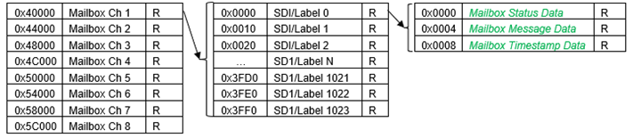
| TIMESTAMP REGISTERS | |||||
| OFFSET | REGISTER NAME | ACCESS | OFFSET | REGISTER NAME | ACCESS |
| 0x100C | Timestamp Control | R/W | 0x1010 | Timestamp Value | R |
| MESSAGE VALIDATION REGISTERS |
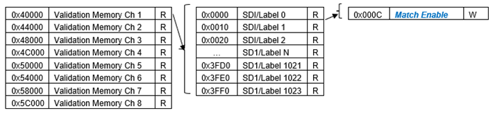
| TRANSMIT FIFO REGISTERS | |||||
| OFFSET | REGISTER NAME | ACCESS | OFFSET | REGISTER NAME | ACCESS |
| 0x1100 | Transmit FIFO Message Buffer Ch 1 | W | 0x1114 | Transmit FIFO Message Count Ch 1 | R |
| 0x1200 | Transmit FIFO Message Buffer Ch 2 | W | 0x1214 | Transmit FIFO Message Count Ch 2 | R |
| 0x1300 | Transmit FIFO Message Buffer Ch 3 | W | 0x1314 | Transmit FIFO Message Count Ch 3 | R |
| 0x1400 | Transmit FIFO Message Buffer Ch 4 | W | 0x1414 | Transmit FIFO Message Count Ch 4 | R |
| 0x1500 | Transmit FIFO Message Buffer Ch 5 | W | 0x1514 | Transmit FIFO Message Count Ch 5 | R |
| 0x1600 | Transmit FIFO Message Buffer Ch 6 | W | 0x1614 | Transmit FIFO Message Count Ch 6 | R |
| 0x1700 | Transmit FIFO Message Buffer Ch 7 | W | 0x1714 | Transmit FIFO Message Count Ch 7 | R |
| 0x1800 | Transmit FIFO Message Buffer Ch 8 | W | 0x1814 | Transmit FIFO Message Count Ch 8 | R |
| 0x110C | Transmit FIFO Almost Empty Threshold Ch 1 | R/W | 0x111C | Transmit FIFO Rate Ch 1 | R/W |
| 0x120C | Transmit FIFO Almost Empty Threshold Ch 2 | R/W | 0x121C | Transmit FIFO Rate Ch 2 | R/W |
| 0x130C | Transmit FIFO Almost Empty Threshold Ch 3 | R/W | 0x131C | Transmit FIFO Rate Ch 3 | R/W |
| 0x140C | Transmit FIFO Almost Empty Threshold Ch 4 | R/W | 0x141C | Transmit FIFO Rate Ch 4 | R/W |
| 0x150C | Transmit FIFO Almost Empty Threshold Ch 5 | R/W | 0x151C | Transmit FIFO Rate Ch 5 | R/W |
| 0x160C | Transmit FIFO Almost Empty Threshold Ch 6 | R/W | 0x161C | Transmit FIFO Rate Ch 6 | R/W |
| 0x170C | Transmit FIFO Almost Empty Threshold Ch 7 | R/W | 0x171C | Transmit FIFO Rate Ch 7 | R/W |
| 0x180C | Transmit FIFO Almost Empty Threshold Ch 8 | R/W | 0x181C | Transmit FIFO Rate Ch 8 | R/W |
| TRANSMIT SCHEDULING REGISTERS |
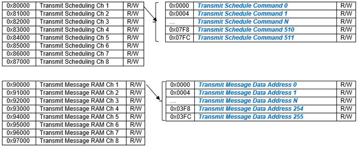
| OFFSET | REGISTER NAME | ACCESS | OFFSET | REGISTER NAME | ACCESS |
| 0x1120 | Async Transmit Data Ch 1 | R/W | |||
| 0x1220 | Async Transmit Data Ch 2 | R/W | |||
| 0x1320 | Async Transmit Data Ch 3 | R/W | |||
| 0x1420 | Async Transmit Data Ch 4 | R/W | |||
| 0x1520 | Async Transmit Data Ch 5 | R/W | |||
| 0x1620 | Async Transmit Data Ch 6 | R/W | |||
| 0x1720 | Async Transmit Data Ch 7 | R/W | |||
| 0x1820 | Async Transmit Data Ch 8 | R/W | |||
| TRANSMIT CONTROL REGISTERS | |||||
| OFFSET | REGISTER NAME | ACCESS | OFFSET | REGISTER NAME | ACCESS |
| 0x1000 | Tx Trigger | R/W | 0x1004 | Tx Pause | R/W |
| 0x1008 | Tx Stop | R/W | |||
| CONTROL REGISTERS | |||||
| OFFSET | REGISTER NAME | ACCESS | OFFSET | REGISTER NAME | ACCESS |
| 0x1118 | Channel Control Ch 1 | R/W | 0x1014 | Module Reset | W |
| 0x1218 | Channel Control Ch 2 | R/W | |||
| 0x1318 | Channel Control Ch 3 | R/W | |||
| 0x1418 | Channel Control Ch 4 | R/W | |||
| 0x1158 | Channel Control Ch 5 | R/W | |||
| 0x1618 | Channel Control Ch 6 | R/W | |||
| 0x1718 | Channel Control Ch 7 | R/W | |||
| 0x1818 | Channel Control Ch 8 | R/W | |||
| BIT REGISTERS | |||||
| *When an event is detected, the bit associated with the event is set in this register and will remain set until the user clears the event bit. Clearing the bit requires writing a '1' back to the specific bit that was set when read (i.e., write-1-to-clear, writing a “1” to a bit set to “1” will set the bit to “0). | |||||
| OFFSET | REGISTER NAME | ACCESS | OFFSET | REGISTER NAME | ACCESS |
| 0x0800 | Dynamic Status | R | |||
| 0x0804 | Latched Status* | R/W | |||
| 0x0808 | Interrupt Enable | R/W | |||
| 0x080C | Set Edge/Level Interrupt | R/W | |||
| 0x02A8 | Test Enabled | R/W | 0x02AC | Power-on BIT Complete++ | R |
| NOTE: ++After power-on, Power-on BIT Complete should be checked before reading the BIT Latched Status. | |||||
| 0x02B8 | Background BIT Threshold | R/W | 0x02BC | Reset BIT | W |
| CHANNEL STATUS REGISTERS | |||||
| OFFSET | REGISTER NAME | ACCESS | OFFSET | REGISTER NAME | ACCESS |
| 0x02B0 | Channel Status Enable | R/W | |||
| *When an event is detected, the bit associated with the event is set in this register and will remain set until the user clears the event bit. Clearing the bit requires writing a '1' back to the specific bit that was set when read (i.e., write-1-to-clear, writing a “1” to a bit set to “1” will set the bit to “0). | |||||
| OFFSET | REGISTER NAME | ACCESS | OFFSET | REGISTER NAME | ACCESS |
| 0x0810 | Dynamic Status Ch 1 | R | 0x0820 | Dynamic Status Ch 2 | R |
| 0x0814 | Latched Status Ch 1* | R/W | 0x0824 | Latched Status Ch 2* | R/W |
| 0x0818 | Interrupt Enable Ch 1 | R/W | 0x0828 | Interrupt Enable Ch 2 | R/W |
| 0x081C | Set Edge/Level Interrupt Ch 1 | R/W | 0x082C | Set Edge/Level Interrupt Ch 2 | R/W |
| 0x0830 | Dynamic Status Ch 3 | R | 0x0840 | Dynamic Status Ch 4 | R |
| 0x0834 | Latched Status Ch 3* | R/W | 0x0844 | Latched Status Ch 4* | R/W |
| 0x0838 | Interrupt Enable Ch 3 | R/W | 0x0848 | Interrupt Enable Ch 4 | R/W |
| 0x083C | Set Edge/Level Interrupt Ch 3 | R/W | 0x084C | Set Edge/Level Interrupt Ch 4 | R/W |
| 0x0850 | Dynamic Status Ch 5 | R | 0x0860 | Dynamic Status Ch 6 | R |
| 0x0854 | Latched Status Ch 5* | R/W | 0x0864 | Latched Status Ch 6* | R/W |
| 0x0858 | Interrupt Enable Ch 5 | R/W | 0x0868 | Interrupt Enable Ch 6 | R/W |
| 0x085C | Set Edge/Level Interrupt Ch 5 | R/W | 0x086C | Set Edge/Level Interrupt Ch 6 | R/W |
| 0x0870 | Dynamic Status Ch 7 | R | 0x0880 | Dynamic Status Ch 8 | R |
| 0x0874 | Latched Status Ch 7* | R/W | 0x0884 | Latched Status Ch 8* | R/W |
| 0x0878 | Interrupt Enable Ch 7 | R/W | 0x0888 | Interrupt Enable Ch 8 | R/W |
| 0x087C | Set Edge/Level Interrupt Ch 7 | R/W | 0x088C | Set Edge/Level Interrupt Ch 8 | R/W |
CANBus Function
Principle of Operation
The onboard CANBus communications function provides the CAN data link layer protocol as standardized in ISO 11898-1 (2003). It can also provide Flexible Data (FD) communication, which is an extension of that ISO standard. The standard describes the data link layer (composed of the logical link control (LLC) sublayer and the media access control (MAC) sublayer) and some aspects of the physical layer of the OSI reference model. All the other protocol layers are the network designer’s choice.
Each CAN node can send and receive messages, but not simultaneously. A message consists primarily of an ID (identifier), which represents the priority of the message, and up to 8 (64 for CAN FD) data bytes. The devices that are connected by a CAN network are typically sensors,actuators, and other control devices. These devices are not connected directly to the bus, but through a host processor and a CAN controller.
If the bus is idle, which is represented by recessive level (Logical 1), any node may begin to transmit. If two or more nodes begin sending messages at the same time, the message with the more dominant ID (which has more dominant bits, i.e., zeroes) will overwrite other nodes’ less dominant IDs, so that eventually (after this arbitration on the ID.) only the dominant message remains and is received by all nodes. This mechanism is referred to as priority-based bus arbitration. Messages with numerically smaller values of IDs have higher priority and are transmitted first.
When utilized, CAN FD communication provides nodes with the capability to send more payload data at faster speeds over a conventional CAN A/B network. The electrical condition/configuration of the CAN Bus (total number of units connected, length of the CAN Bus wires, other electromagnetic factors) determine the fastest data transfer rate possible on that CAN Bus. It also provides better error detection in received CAN messages.
Each node (the CAN module on an appropriate board/system platform is a node) provides:
Host Module Processing
The host (on-module) processor decides what received messages mean and which messages it wants to transmit itself. Sensors, actuators, and control devices can be connected to the host processor.
For the NIU3x devices (NIU3A and NIU3E), 4 channels of CAN-FD are available. Each channel can be viewed as a separate CAN Bus. The BareMetal application that runs on the NIU3x processor not only services the CAN-FD module functionality but also services all other “inboard” module functionality (such as Discrete I/O, ARINC-429, and MIL-STD-1553).
The BareMetal application has a control loop that services each of these inboard modules sequentially in a single thread. Each module has a different amount of functionality to be performed when it is their turn to run. Regarding CAN-FD functionality, for versions of the BareMetal where the Enhanced Last Error Code compatibility bit is not set, the BareMetal application will cycle through all channels checking for incoming commands, in addition to performing any Rx and Tx actions for each channel before it relinquishes processing control. For BareMetal versions that have the Enhanced Last Error Code compatibility bit set, the BareMetal application will only process one (target) channel on any given pass before relinquishing processing control. This ‘target channel to process’ moves to the next channel so during the next CAN-FD run period, a different target channel is processed. The reason for this “round-robin” approach to processing the CAN channels is that CAN-FD processing was determined to be taking longer than was expected due to the processing of all four channels before relinquishing control. By processing only an individually selected channel during a run period, the other modules are now processed in a timelier manner, reducing the overall processing loop time.
Another factor impacting the amount of time spent processing CAN-FD is the frequency of messages that need to be sent or received during the CAN-FD processing cycle for the channel(s) being processed. The BareMetal application for CAN-FD measures MAX_WORK_TIME in milliseconds (ms). The ‘non-round-robin’ versions of the BareMetal code contain a default value of 1000ms (approximately 1 second). Users of these versions of the BareMetal can set this MAX_WORK_TIME to any value from 0 to 4,294,967,295 (max unsigned integer 32-bit value). If set to 0, however, the ‘non-round-robin’ versions of the BareMetal will automatically assign the MAX_WORK_TIME to the default value (1000ms). The least amount of time the user can set the MAX_WORK_TIME to be is 1ms.
This logic was changed with the ‘round-robin version’ of the BareMetal. Now, the default MAX_WORK_TIME in milliseconds is 0. This means that when transmitting or receiving CAN-FD messages, the most that will be processed is 1 message before CAN-FD relinquishes processing control. During each CAN-FD processing cycle, the control register is checked for any requested commands to be performed (bit by bit). If any bits return a value of 1, that command’s desired action is performed. When the action is finished, the corresponding control bit is set back to 0 to indicate that the action was completed by the BareMetal functionality. After all the applicable control bits are processed, a check is made to see if transmit for the channel being processed is enabled. If transmit is enabled, the BareMetal will try to transmit data found in the transmit FIFO. After transmitting each full message, a timer is checked to see how long has been spent in the transmit function. If this time exceeds the MAX_WORK_TIME, the transmit function will exit even if there is still additional data in the transmit FIFO to send. This time limit helps to prevent delaying the other function modules from being serviced.
After the transmit function is finished, the receive function is called, which probes the CAN-FD IP to determine if any messages are available for retrieval. If there are available messages for retrieval, a logic like what is used for the transmit function regarding the MAX_WORK_TIME allowed is performed. Full CAN-FD messages are read from the CAN-FD IP and copied to the receive FIFO. The retrieval of messages will continue if there are messages to be received or until the MAX_WORK_TIME has been exceeded. In either case the receive function will exit and the CAN-FD will relinquish control back to the BareMetal main routine allowing the next function module in queue to be processed.
CAN Controller: Hardware with a Synchronous Clock
Receiving: the CAN controller stores received bits serially from the bus until an entire message is available and put in the FIFO, which can then be fetched by the host processor (usually after the CAN controller has triggered an interrupt or is polling for messages).
Sending: the host processor stores the transmit messages onto a CAN controller, which transmits the bits serially onto the bus.
Transceiver
Receiving: it adapts signal levels from the bus to levels that the CAN controller expects and has protective circuitry that protects the CAN controller.
Transmitting: it converts the transmit-bit signal received from the CAN controller into a signal that is sent onto the bus. With CAN A/B, bit rates up to 1 Mbit/s are possible at network lengths below 40 m. Decreasing the bit rate allows longer network distances (e.g., 500 m at 125 kbit/s). With CAN FD, bit rates up to 4 Mbit/s are possible at network lengths below 40 m (Note: this is for data payload only; the arbitration bit rate is still limited to 1Mbit/s for compatibility). Decreasing the bit rate allows longer network distances (e.g., 500 m at 125 kbit/s). CAN FD extends the speed of the data section by a factor of up to 8 (64 bytes) of the arbitration bit rate over what classic CAN provides (8 bytes). The CAN FD frame/message ID uses an Extended ID (29-bit format) version of the classic CAN Standard ID (11-bit) format. CAN FD can also handle Standard ID format messages, as well.
As applications may require many nodes (SG), which are not predetermine, both conventional CAN A/B bus and CAN-FD bus require proper termination (120-ohm resistor at each end of the bus) to operate properly. A new feature to NAI’s CAN-FD module is the ability to assign termination to desired channels in code rather than requiring a physical resistor to be attached.
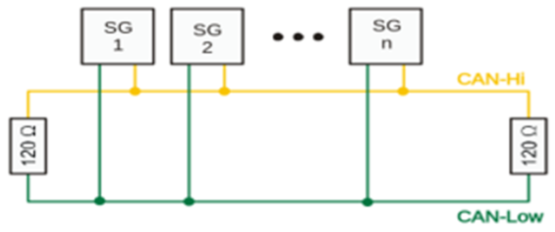
Continuous Background Built-in Test (BIT)/Diagnostic Capability
BIT is performed in the background continuously within the FPGA. Each channel is checked periodically at 80MHz for correct operation. Any failure triggers an interrupt if enabled, with the results available in the status registers. The testing is transparent to the user and has no effect on the operation of the onboard CANBus function.
Register Descriptions
The register descriptions provide the register name, Register Offset, Type, Data Range, Read or Write information, Default Value, a description of the function and, in most cases, a data table.
Receive Registers
The registers listed are associated with data that is received on the CANBus channels
| Receive FIFO Buffer Data | |
| Function: | Stores received messages. |
| Type: | unsigned binary word (32-bit) |
| Data Range: | 0x0000 0000 to 0xFFFF FFFF |
| Read/Write: | W-H, R-A NOTE: 'H' is 'Host; 'A' is 'ARM' |
| Operational Settings: | N/A |
| Default: | 0 |
CAN Frame as it is to be read off the FIFO - The FIFO contains 32-bit values where the top 8 bits are reserved for flags. The payload is “packed” where up to 3 x 8-bit values are stuffed into 1 x 32-bit read from the FIFO (upper 8 bits are always reserved for flags)
| Description | Bits Read | Meaningful Bits | NOTES |
| Msg ID - Lower 16 | 32 | Lower 16 (0x0000FFFF) | Lower and Upper make up 29 Bit Identifier |
| Msg ID - Upper 16 | 32 | Upper 16 (0x0000FFFF) | |
| Timestamp - Lower 16 | 32 | Lower 16 (0x0000FFFF) | Lower and Upper Timestamp |
| Timestamp - Upper 16 | 32 | Upper 16 (0x0000FFFF) | |
| Msg/Payload Length | 32 | 1 Byte (0x000000FF) | Length of Msg (payload count) |
| Payload Data is “Packed” - lower 24 bits make up 3 x 8 bits of data. Top 8 bits are reserved for flags. | |||
| Data[0], Data[1], Data[2] | 32 | ||
| Data[0] | X | 1st Byte (0x000000FF) | 1st Byte is Data[0] |
| Data[1] | X | 2nd Byte (0x0000FF00) | 2nd Byte is Data[1] |
| Data[2] | X | 3rd Byte (0x00FF0000) | 3rd Byte is Data[2] |
| If msg length indicates more data to read…another 32 bits would be read from the FIFO | |||
| Data[3], Data[4], Data[5] | 32 | ||
| Data[3] | X | 1st Byte (0x000000FF) | 1st Byte is Data[3] |
| Data[4] | X | 2nd Byte (0x0000FF00) | 2nd Byte is Data[4] |
| Data[5] | X | 3rd Byte (0x00FF0000) | 3rd Byte is Data[5] |
| This continues until Data[MsgLen -1] |
| Receive FIFO Word Count | |
| Function: | Contains the number of 32-bit words in the Receive FIFO buffer. |
| Type: | unsigned integer word |
| Data Range: | 0 to 1024 (0 to 0x0000 0400) |
| Read/Write: | R |
| Operational Settings: | N/A |
| Default: | 0 |
| Receive FIFO Frame Count | |
| Function: | Contains the number of frames in the Receive FIFO buffer. |
| Type: | unsigned integer word |
| Data Range: | 0 to 204 (0 to 0x0000 00CC) (Minimum CAN frame will be 5 entries on the FIFO) |
| Read/Write: | R |
| Operational Settings: | Each minimum CAN frame is 5; 32-bit words that get placed on the FIFO. Maximum frame count is thus 1024 (0x0000 0400) / 5 = 204 (0x0000 00CC). |
| Default: | 0 |
Transmit Registers
The registers listed are associated with data that is transmitted on the CANBus channels.
| Transmit FIFO Buffer Data | |
| Function: | Transmits messages in FIFO |
| Type: | unsigned binary word (32-bit) |
| Data Range: | 0x0000 0000 to 0xFFFF FFFF |
| Read/Write: | W-H, R-A NOTE: 'H' is 'Host; 'A' is 'ARM' |
| Operational Settings: | N/A |
| Default: | 0 |
CAN Frame as it is to be read off the FIFO - The FIFO contains 32-bit values where the top 8 bits are reserved for flags. The payload is “packed” where up to 3 x 8-bit values are stuffed into 1 x 32-bit read from the FIFO (upper 8 bits are always reserved for flags)
| Description | Bits Read | Meaningful Bits | NOTES |
| Protocol | 32 | 0xFF00000F | Valid Protocol values are 0 and 1. Flag for Start of message is 0x80000000 |
| Msg ID - Lower 16 | 32 | Lower 16 (0x0000FFFF) | Lower and Upper make up 29 Bit Identifier |
| Msg ID - Upper 16 | 32 | Upper 16 (0x0000FFFF) | |
| Extended ID | 32 | 0x0000000F | Mode A = 0 Extended = 1 |
| Msg/Payload Length | 32 | 1 Byte (0x000000FF) | Length of Msg (payload count). If zero payload, the End of Message Flag (0x10000000) will be set |
| Payload Data is “Packed” - lower 24 bits make up 3 x 8 bits of data. Top 8 bits are reserved for flags. | End of Message Flag (0x10000000) will be set on the last payload data value only. | ||
| Data[0], Data[1], Data[2] | 32 | ||
| Data[0] | X | 1st Byte (0x000000FF) | 1st Byte is Data[0] |
| Data[1] | X | 2nd Byte (0x0000FF00) | 2nd Byte is Data[1] |
| Data[2] | X | 3rd Byte (0x00FF0000) | 3rd Byte is Data[2] |
| If msg length indicates more data to read…another 32 bits would be read from the FIFO | |||
| Data[3], Data[4], Data[5] | 32 | ||
| Data[3] | X | 1st Byte (0x000000FF) | 1st Byte is Data[3] |
| Data[4] | X | 2nd Byte (0x0000FF00) | 2nd Byte is Data[4] |
| Data[5] | X | 3rd Byte (0x00FF0000) | 3rd Byte is Data[5] |
| This continues until Data[MsgLen -1] |
| Transmit FIFO Word Count | |
| Function: | Contains the number of 32-bit words in the Transmit FIFO register. |
| Type: | unsigned integer word |
| Data Range: | 0 to 1024 (0 to 0x0000 0400) |
| Read/Write: | R |
| Operational Settings: | N/A |
| Default: | 0 |
| Transmit FIFO Frame Count | |
| Function: | Contains the number of frames in the Transmit FIFO register. |
| Type: | unsigned integer word |
| Data Range: | 0 to 204 (0 to 0x0000 00CC) (Minimum CAN frame will be 5 entries on the FIFO) |
| Read/Write: | R |
| Operational Settings: | Each minimum CAN frame is 5; 32-bit words that get placed on the FIFO. Maximum frame count is thus 1024 (0x0000 0400) / 5 = 204 (0x0000 00CC). |
| Default: | 0 |
Command Registers
The registers listed are associated with functionality which enables Tx and Rx FIFO to be dedicated to sending and receiving CAN-FD messages.
| BareMetal Capabilities Register | |
| Function: | Determines if the revision of BM can use Command FIFO, response registers and can set the device sample point. |
| Type: | unsigned integer word |
| Data Range: | 0 or 1 |
| Read/Write: | R/W |
| Operational Settings: | See table below |
| Default: | 0 |
| D31 | D30 | D29 | D28 | D27 | D26 | D25 | D24 | D23 | D22 | D21 | D20 | D19 | D18 | D17 | D16 |
| 0 | 0 | 0 | 0 | 0 | 0 | 0 | 0 | 0 | 0 | 0 | 0 | 0 | 0 | 0 | 0 |
| D15 | D14 | D13 | D12 | D11 | D10 | D9 | D8 | D7 | D6 | D5 | D4 | D3 | D2 | D1 | D0 |
| 0 | 0 | 0 | 0 | 0 | 0 | 0 | 0 | 0 | 0 | 0 | 0 | D | D | D | D |
| Bit | Description |
| D0 | Cmd FIFO in Use: if set to 1, Cmd FIFO is available and can be used to send parameters to the BareMetal. |
| D1 | Sample Point: If set to 1, the BareMetal is capable of setting or changing the sample point. |
| D2 | Response Registers: If set to 1, the BareMetal is using these registers to return data instead of the Rx FIFO. |
| D3 | Enhanced Last Error Code: If set to 1, the BareMetal has enhanced logic surrounding the reporting of the last error. This change was made at the same time a change was made to process each channel in a 'round-robin' approach as well as a change to make the default MAX_WORK_TIME value 0 ms in the BareMetal as opposed to the former default value of 1000 ms. With this compatibility bit set to 1, a user can expect less processing time spent servicing the CAN-FD module on each “cycle” when compared to BareMetal versions that do not have this compatibility bit set to 1. |
| Command FIFO Buffer Data | |
| Function: | Transmits BareMetal parameters in FIFO |
| Type: | unsigned binary word (32-bit) |
| Data Range: | 0 to 0xFFFF FFFF |
| Read/Write: | W-H, R-A NOTE: 'H' is 'Host; 'A' is 'ARM' |
| Operational Settings: | N/A |
| Default: | 0 |
| Command FIFO Word Count | |
| Function: | Contains the number of words in the Command FIFO register. |
| Type: | unsigned integer word |
| Data Range: | 0 to 1024 (0 to 0x0000 0400) |
| Read/Write: | R |
| Operational Settings: | N/A |
| Default: | 0 |
Control Registers
The register specified in this section provides the ability to control the operation for each CANBus channel.
Control
The control register has been implemented to act solely as a “request for action” register. Bits can be set to a 1 to request various actions or capabilities. When the action or capability is acted upon by the CAN firmware, these request bits will be set back to 0.
| Control | |
| Function: | Provides flags for controlling transmit and receive activity. |
| Type: | binary word (32-bit) |
| Data Range: | 0x0000 0000 to 0x00FF FFFF |
| Read/Write: | R/W |
| Operational Settings: | See descriptions that follow. |
| Default: | 0 (disabled) |
| D31 | D30 | D29 | D28 | D27 | D26 | D25 | D24 | D23 | D22 | D21 | D20 | D19 | D18 | D17 | D16 |
| D | 0 | 0 | 0 | 0 | D | D | D | D | D | D | D | D | D | D | D |
| D15 | D14 | D13 | D12 | D11 | D10 | D9 | D8 | D7 | D6 | D5 | D4 | D3 | D2 | D1 | D0 |
| D | 0 | D | D | D | D | D | D | 0 | 0 | D | D | 0 | 0 | D | D |
| Bit | Description |
| D0 | Request Enable Tx: Enables any messages found in the Tx FIFO to be placed on the bus from the current channel. |
| D1 | Request Disable Tx: Stops any messages currently in the Tx FIFO from being put on the bus from the current channel. |
| D2 | RESERVED FOR FUTURE |
| D3 | RESERVED FOR FUTURE |
| D4: | Request Set Level Dominant: This is for Debug purposes only and forces channel bus signal to a constant dominant value. |
| D5 | Request Set Level Recessive: This is for Debug purposes only and forces channel bus signal to a constant recessive value. |
| D6 | Request Enable Termination: Internal termination will be enabled for the current channel. |
| D7 | Request Disable Termination: Internal termination will be disabled for the current channel. |
| D8 | Request Base Rate Change: Desired base rate enumerated type value needs to be assigned to the lower 16 bits of the datarate-baserate register. Valid values include 0 (1Mb), 1 (500K), 3 (250K), 7 (125K) and 9 (83.33K) |
| D9 | Request Data Rate Change: Desired data rate enumerated type value needs to be assigned to the upper 16 bits of the datarate-baserate register. Valid values include 6 (4Mb), 7 (3Mb), 8 (2Mb) and 9 (1Mb). NOTE: Data rate of 3 Mb is not recommended as it has been found to be unreliable. |
| D10 | Request reset of Tx FIFO: Clears the entire Tx FIFO |
| D11 | Request reset of Rx FIFO: Clears the entire Rx FIFO |
| D12 | Request reset of Drop Count: Resets the counter that keeps track of how many messages were dropped due to FIFO already being full. |
| D13 | Request reset of Command FIFO: Clears the entire Command FIFO. |
| D14: | RESERVED FOR FUTURE |
| D15 | Request Reset Channel. Expected for next release: Reset Channel will reset both the Tx, Rx and Cmd FIFOs, disable Tx enable, Clear any Last Error Code, zero out Tx/Rx error counter and drop count registers and reset entire set of response registers. Reset Channel also retains the configured baud rate so the baud rates that were configured prior to the reset will be reassigned after the reset completes back to the same baud rates. |
| D16: | Request Config Sequencer: Allows caller to configure a given sequencer (schedule). Configuration data is expected to be placed on the Tx FIFO in the following order: (1) Requested Config Sequencer Cmd ID so we know the data following this is the data needed to configure a new sequencer/schedule. (2) Sequencer ID (schedule index): 1 based value of schedule to configure. (3) Protocol: 0 (CAN A/B) or 1 (CAN FD) (4) Rate: The number of 125us between two transmissions (5) Skew: The number of 125us after the rate event to transmit the message. (Example: If the rate is 80, then the message is transmitted every 10ms. If two messages have the same rate then it may be wise to stagger the messages a little to avoid collision by setting the skew for the 1 message to 0 and the skew for the 2 message to 2 where 2 * 125us = 250us. (6) MsgID (low): place lowest 16 bits of MsgID onto FIFO. (7) MsgID (high): place highest 13 bits of MsgID onto FIFO (zeros if CAN A/B). (8) Extended ID: 0 (Not Extended 11bit identifier), 1 (Extended 29bit identifier) (9) Msg (payload) Length: value between 0 and 64 if CAN FD or 0 and 8 if CAN A/B (10) Msg payload starts..should have Msg Length number of values in the FIFO waiting to be read into a buffer. |
| D17 | Request Start Sequencer/Scheduler: This will start all configured sequencers/schedules |
| D18 | Request Stop Sequencer/Scheduler: This will stop all configured sequencers/schedules |
| D19 | Set Sample Point: Provides flexibility to assign various sample point values (75% or 80%) to the CAN FD core since it is important that all CAN FD devices use the same sample point to detect bit rate switching (BRS). |
| D20 | Request Enable Filters: Enables all filters configured for the current channel. |
| D21 | Request Disable Filters: Disables all filters configured for the current channel. |
| D22 | Request Set Filter: Allows caller to configure a filter (A total of 8 filters can be configured indexed from 0 - 7). Filter configuration data is expected to be placed on the Cmd FIFO in the following order: (1) Set Filter Cmd ID: so we know the data following this is the data needed to configure a new filter. (2) Filter Index: A value between 0 and 7 (filter slot to configure). (3) CAN ID (low): low 16 bits of CAN ID. (4) CAN ID (high): the highest 16 bits of CAN ID (pushed to the lower 16 bits of this FIFO value). (5) Extended ID: 1 to only allow extended ID messages, 0 normal CAN A/B messages (6) First Byte of Payload to filter on (8 bits) (7) 2 Byte of Payload to filter on (8 bits) |
| D23 | Request Get Filter: Retrieves desired filter data. The following is expected to be on the Cmd FIFO when this control bit value is detected being set: (1) Get Filter Cmd ID: so we know the data following this is the data needed to get desired filter information. (2) Filter Index: A value between 0 and 7 of which to fetch filter configuration data. NOTE: The response data will be made available in the set of response registers. |
| D24 | Request Set Filter Mask: The following data is expected to be on the Cmd FIFO in order to configure the desired Filter Mask. The Filter Mask is used on incoming messages that are received and on the corresponding Filter configuration data that was set where Filter Index = Mask Index. After applying the mask to both, the corresponding bits are compared and if both sides match, the data is received else it is rejected. (1) Set Filter Mask Cmd ID: so we know the data following this is the data needed to configure a new filter mask. (2) Mask Index: A value between 0 and 7 (mask slot to configure). NOTE: Mask index is meant to align with desired Filter Index from Set Filter. (3) CAN ID (low): low 16 bits of CAN ID. (4) CAN ID (high): the highest 16 bits of CAN ID (pushed to the lower 16 bits of this FIFO value). (5) Extended ID: 1 to only allow extended ID messages, 0 normal CAN A/B messages (6) First Byte of Payload to filter on (8 bits) (7) 2 Byte of Payload to filter on (8 bits) |
| D25 | Request Get Filter Mask: Retrieves desired filter mask configuration data. The following is expected to be on the Cmd FIFO when this control bit value is detected being set: (1) Get Filter Mask Cmd ID: so we know the data following this is the data needed to get desired filter mask information. (2) Mask Index: A value between 0 and 7 of which to fetch mask configuration data. NOTE: The response data will be made available in the set of response registers for the given channel. |
| D26 | Request Remove Filter: Removes desired filter from the filter configuration. The following is expected to be on the FIFO when this control bit is detected being set: (1) Remove Filter Cmd ID: so we know the data following this is the data needed to remove desired filter information. (2) Filter Index: A value between 0 and 7 (filter slot to remove filter configuration) |
| D27 | RESERVED FOR FUTURE |
| D28 | RESERVED FOR FUTURE |
| D29 | RESERVED FOR FUTURE |
| D30 | RESERVED FOR FUTURE |
| D31 | Config edit flag when set to a 1 it indicates end-user is currently editing the control register and we should not yet act upon set values. If 0, all bits in the control register will be evaluated and acted upon. |
| Data Rate/Base Rate | |
| Function: | Indicates the current rate (speed) at which data is being transmitted on the CAN network. User applications should always specifically configure the Baud Rates for each active channel and not rely on the default values set within the BareMetal. |
| Type: | unsigned binary word (32-bit) |
| Data Range: | Lower 16 bits range is 0 - 3...Upper 16 bits range is from 6 - 9. |
| Read/Write: | R/W |
| Operational Settings: | Upper 16 bits dedicated to data rate enumerated type value; Lower 16 bits dedicated to base rate enumerated type value. NOTE: Data Rate is applicable only when the protocol is set to CAN FD; Base Rate is utilized by both CAN A/B and CAN FD. |
| Default: | 0 for Base Rate; 8 for Data Rate |
| Data Rate (CAN FD only) | |||||||||||||||
| D31 | D30 | D29 | D28 | D27 | D26 | D25 | D24 | D23 | D22 | D21 | D20 | D19 | D18 | D17 | D16 |
| D | D | D | D | D | D | D | D | D | D | D | D | D | D | D | D |
| Base Rate | |||||||||||||||
| D15 | D14 | D13 | D12 | D11 | D10 | D9 | D8 | D7 | D6 | D5 | D4 | D3 | D2 | D1 | D0 |
| D | D | D | D | D | D | D | D | D | D | D | D | D | D | D | D |
| Valid values for Base Rate currently include: | |
| 0: | 1Mb (1000K) Base Baud |
| 1: | 500K Base Baud |
| 3: | 250K Base Baud |
| 7: | 125K Base Baud |
| 9: | 83.33 Base Baud |
| Valid values for Data Rate currently include: | |
| 6: | 4Mb (4000K) Data Baud |
| 7: | 3Mb (3000K) Data Baud |
| 8: | 2Mb (2000K) Data Baud |
| 9: | 1Mb (1000K) Data Baud |
Note
Data rate of 3 Mb is not recommended as it has been found to be unreliable.
| Sample Point | |
| Function: | Indicates the sample point to be used. Different 3rd party vendor equipment may use different sample points. This register provides some flexibility to the NAI CAN FD functionality. |
| Type: | unsigned binary word (32-bit) |
| Data Range: | 0 (75%) to 0x0000 0001 (80%) |
| Read/Write: | R/W |
| Operational Settings: | The sample point can be set to 75% or 80% depending on which value works best for the CAN FD operational environment |
| Default: | 0x0000 0001 (80%) |
| RxMaxWorkTimeMS | |
| Function: | Defines length of time user will wait to perform receiving of CAN FD messages before processing control is returned to all other processing. NOTE: A value of zero forces the default value of 1000ms to be used if the Enhanced Last Error Code capabilities bit is not set in the Baremetal Capabilities register. If it is desired to spend as little time as possible, this value should be set to 0x00000001. If the Enhanced Last Error Code capabilities bit is set, the default value of 0 ms is used and is the recommended value to spend as little time as possible. |
| Type: | unsigned binary word (32-bit) |
| Data Range: | 0 to 0xFFFF FFFF |
| Read/Write: | R/W |
| Operational Settings: | 1000ms / 0ms |
| Default: | 1000ms (if Enhanced Last Error Code capabilities bit is 0); 0ms (if Enhanced Last Error Code capabilities bit is 1) |
| TxMaxWorkTimeMS | |
| Function: | Defines length of time user will wait to perform transmitting of CAN FD messages before processing control is returned to all other processing. NOTE: A value of zero forces the default value of 1000ms to be used if the Enhanced Last Error Code capabilities bit is not set in the Baremetal Capabilities register. If it is desired to spend as little time as possible, this value should be set to 0x00000001. If the Enhanced Last Error Code capabilities bit is set, the default value of 0 ms is used and is the recommended value to spend as little time as possible. |
| Type: | unsigned binary word (32-bit) |
| Data Range: | 0 to 0xFFFF FFFF |
| Read/Write: | R/W |
| Operational Settings: | 1000ms / 0ms |
| Default: | 1000ms (if Enhanced Last Error Code capabilities bit is 0); 0ms (if Enhanced Last Error Code capabilities bit is 1) |
Message Status/Monitoring Registers
The registers specified in this section provide status and monitoring information on about the CANBus messages.
| FIFO Status | |
| Function: | Describes current FIFO Status. |
| Type: | unsigned binary word (32-bit) |
| Data Range: | NA |
| Read/Write: | R |
| Operational Settings: | See table below. |
| Default: | 0 |
| Bit | Description | Configurable? |
| D0 | Rx FIFO EMPTY: When set to 1: Rx FIFO is empty. | No |
| D1 | Rx FIFO ALMOST EMPTY: When set to 1: Rx FIFO is at 20% capacity. | No |
| D2 | Rx FIFO ALMOST FULL: When set to 1: Rx FIFO is at 80% capacity. | No |
| D3 | Rx FIFO FULL: When set to 1: Rx FIFO is full. | No |
| D4 | Tx FIFO EMPTY: When set to 1: Tx FIFO is empty. | No |
| D5 | Tx FIFO ALMOST EMPTY: When set to 1: Tx FIFO is at 20% capacity. | No |
| D6 | Tx FIFO ALMOST FULL: When set to 1: Tx FIFO is at 80% capacity. | No |
| D7 | Tx FIFO FULL: When set to 1: Tx FIFO is full. | No |
| Last Error Code (LEC) | |
| Function: | Stores the value of the last detected error. NOTE: this is a single value so if multiple errors occur prior to this register being read, only the last error value will be present. |
| Type: | signed binary word (32-bit) if compatibility bit D3 from BareMetal Capabilities Registers is 0 (Non-Enhanced Error Code) unsigned binary word (32-bit) if compatibility bit D3 from BareMetal Capabilities Register is 1 (Enhanced Error Code) |
| Data Range: | 0 = success negative value = failure |
| Read/Write: | R/W (to allow register to be cleared) |
| Operational Settings: | The last error code to be received on a channel. |
| Default: | 0 |
| D31 | D30 | D29 | D28 | D27 | D26 | D25 | D24 | D23 | D22 | D21 | D20 | D19 | D18 | D17 | D16 |
| D | D | D | D | D | D | D | D | D | D | D | D | D | D | D | D |
| D15 | D14 | D13 | D12 | D11 | D10 | D9 | D8 | D7 | D6 | D5 | D4 | D3 | D2 | D1 | D0 |
| D | D | D | D | D | D | D | D | D | D | D | D | D | D | D | D |
| Common Error Values (when Non-Enhanced Error Code): | |
| -50: | INVALID_DEVICE_NUMBER |
| -65: | INVALID PARAMETER |
| -1009: | MESSAGE NOT DETECTED |
| Full List of Error Values when Enhanced Error Code: | |
| (HEX) | Error Description |
| 0x0001 | NAI_BUS ERROR Bus Errors can happen for multiple reasons. Most often are Baud Rate mismatches. Check all devices on the bus to make sure they are all running the same baud rates (both config and data for CAN-FD or only config for CAN A/B). Bus Error can also take place if the bus is not properly terminated. Check the termination and/or configure the FPGA termination via the NAI SSK library functionality. Bus Errors can also happen if there is only 1 device on the bus. CAN-FD needs at least 2 devices on the bus in order to function appropriately. |
| 0x0002 | NAI_SEQUENCER_START_ERROR This error is reported if there is a problem enabling the sequencer. Sequencer can additionally be thought of as a schedule and can be configured to TX data at a desired frequency. |
| 0x0003 | NAI_SEQUENCER_STOP_ERROR This error is reported if there is a problem stopping (or disabling) the sequencer. |
| 0x0004 | NAI_SEQUENCER_INDEX_ERROR Sequencer index errors may occur if a sequence index that is out-of-range is attempted to be configured. Valid index range is from 1 - 31 inclusive. |
| 0x0005 | NAI_SET_DEVICE_MODE_ERROR The BareMetal logic for CAN-FD will force the CAN-FD IP to be in different modes under certain circumstances (like monitor mode or normal mode). If the IP fails to enter these modes when requested, this error will be raised. |
| 0x0006 | NAI_BAUD_RATE_CHANGE_ERROR If the CAN-FD IP fails to enter the baud rate being requested, this error will be raised. |
| 0x0007 | NAI_ENABLE_FILTERS_ERROR This error is reported if the CAN-FD IP fails to enable the filters when a request is made. |
| 0x0008 | NAI_DISABLE_FILTERS_ERROR This error is reported if the CAN-FD IP fails to disable the filters when a request is made. |
| 0x0009 | NAI_MISSING_END_OF_MSG_ERROR This error is reported if when reading a CAN message off the TX FIFO, the end of message delimiter is not found. |
| 0x000A | NAI_INSUFFICIENT_DATA_ERROR This error is reported when a given command (control register bit set to a 1) requires additional information, and that additional information was not found to be included. Older versions of the BareMetal code used the TX FIFO as the transfer mechanism from the user application to the BareMetal. Newer versions of the BareMetal have a separate Command FIFO that is used. In either case, if the BareMetal does not see all the information it expects on the FIFO being used, this error will be raised. |
| 0x000B | NAI_EXPECTED_CMD_NOT_FOUND_ERROR As discussed in the prior error regarding NAI_INSUFFICIENT_DATA_ERROR, when a control register bit is set to a 1 and the command associated with that bit requires additional information, a FIFO is used as the transport mechanism from the user application to the BareMetal application. The first piece of information the BareMetal looks for is the Command ID to make sure the data being passed on the FIFO matches the command we are looking to get additional information about. If the Command ID read off the FIFO does not match the command associated with the control register bit that we are currently processing, this error is raised. |
| 0x000C | NAI_INIT_DEVICE_ERROR This error is reported if the CAN-FD IP fails to initialize the given CAN-FD device. (Each channel of the CAN-FD will have its own device ID) |
| 0x000D | NAI_OPEN_DEVICE_ERROR This error is reported if the CAN-FD IP fails to open the given CAN-FD device. (Each channel of the CAN-FD will have its own device ID) |
| 0x000E | NAI_NO_ROOM_ON_RX_FIFO_ERROR This error is raised if when receiving a CAN message, it is determined that there is not enough room to put the entire message on the Rx FIFO. This can happen if the Rx FIFO fills up. The BareMetal will not put a partial message on the Rx FIFO. If the entire message won't fit, the BareMetal will report this error and stop attempting to receive more CAN messages. |
| 0x0010 | NAI_FILTER_INDEX_ERROR This error is raised if the filter index on the BareMetal side is found to be > 7. The BareMetal application expects filter index to be in the range of 0 to 7 inclusive (Max of 8 Filter Indexes). |
| 0x0011 | NAI_SET_FILTER_ERROR This error is raised if the CAN-FD IP fails to set the filter information for the specified filter index. |
| 0x0012 | NAI_GET_FILTER_ERROR This error is raised if the CAN-FD IP fails to get the filter information for the specified filter index. |
| 0x0013 | NAI_SET_FILTER_MASK_ERROR This error is raised if the CAN-FD IP fails to set the filter mask information for the specified filter mask index. |
| 0x0014 | NAI_GET_FILTER_MASK_ERROR This error is raised if the CAN-FD IP fails to get the filter mask information for the specified filter mask index. |
| 0x0015 | NAI_REMOVE_FILTER_ERROR This error is raised if the CAN-FD IP fails to remove the filter information associated with the specified filter index. |
| 0x0020 | NAI_IP_GENERAL_API_ERROR The NAI_IP_GENERAL_API_ERROR is a general error that will be raised when internal calls into the CAN-FD IP are made and return an IP failure status. |
| 0x0021 | NAI_IP_TX_FIFO_FULL This error is raised if the CAN-FD IP signals that its own Tx FIFO within the IP is full. |
| 0x0022 | NAI_IP_RX_FIFO_FULL This error is raised if the CAN-FD IP signals that its own Rx FIFO within the IP is full. |
| Drop Count | |
| Function: | Every time a received message is unable to be placed onto the Rx FIFO because the FIFO is full, the message will be dropped, and this register's value will be incremented by 1. This Drop count can be reset by sending the request to reset the drop count command via the control register (see data bit 12 (D12) of the control register description). |
| Type: | unsigned binary word (32-bit) |
| Data Range: | 0 - 0xFFFF FFFF |
| Read/Write: | R/W |
| Operational Settings: | Drop Count |
| Default: | 0 |
| D31 | D30 | D29 | D28 | D27 | D26 | D25 | D24 | D23 | D22 | D21 | D20 | D19 | D18 | D17 | D16 |
| D | D | D | D | D | D | D | D | D | D | D | D | D | D | D | D |
| D15 | D14 | D13 | D12 | D11 | D10 | D9 | D8 | D7 | D6 | D5 | D4 | D3 | D2 | D1 | D0 |
| D | D | D | D | D | D | D | D | D | D | D | D | D | D | D | D |
| Tx/Rx Error Counter | |
| Function: | This register exposes the Tx Errors and Rx Errors reported by the CAN IP (intellectual property). The Tx Error Count is shifted up 16 bits starting at bit D16 and the Rx Error Count starts at bit D0. Both the Tx and Rx Error Counts have a max value of 255. |
| Type: | unsigned binary word (32-bit) |
| Data Range: | 0 - 0x00FF 00FF |
| Read/Write: | R/W |
| Operational Settings: | Tx/Rx Error Counter |
| Default: | 0 |
| D31 | D30 | D29 | D28 | D27 | D26 | D25 | D24 | D23 | D22 | D21 | D20 | D19 | D18 | D17 | D16 |
| 0 | 0 | 0 | 0 | 0 | 0 | 0 | 0 | D | D | D | D | D | D | D | D |
| D15 | D14 | D13 | D12 | D11 | D10 | D9 | D8 | D7 | D6 | D5 | D4 | D3 | D2 | D1 | D0 |
| 0 | 0 | 0 | 0 | 0 | 0 | 0 | 0 | D | D | D | D | D | D | D | D |
Status and Interrupt Registers
The registers may be set for any or all channels and will latch if a transition is detected on a channel or channels. Each channel(s) will remain latched until the channel is cleared. Multiple channels may be cleared simultaneously, if desired. Each channel bit in the register is polled for a read status. Any subsequent channel(s) transition, if detected, will propagate through to be read (rolling-latch).
Once the status register has been read, the act of writing a 1 back to the applicable status register to any specific bit (channel) location (bit-mapped per channel), will “clear” the bit (set the bit to 0) if the actual interruptible event condition has cleared. If the interruptible condition “event” is still persistent while clearing, this may retrigger the interrupt.
There is a corresponding Interrupt Enable and vector associated with each “Latched” Status. Each status type may be “polled” (at any time) or is “interruptible” when interrupts are enabled and the associated Interrupt Service Routine (ISR) vectors are programmed accordingly. When programmed for “interruptible” status, interrupts are typically generated and flagged with the programmed vector available as data. The host or single board computer (SBC) typically services the interrupt by a general or specific ISR, which reads the (typically) unique programmed vector (identifier of which status generated the interrupt), reads the associated status register to determine which channel in the status register was “flagged” and then “clears” the status register. This essentially resets the interrupt mechanism, which is now ready to be triggered by the next status register detected event “flag”. “Latched Status” will trigger on either “sense on edge” or “sense on level” based on the settings of the associated Set Edge/Level Interrupt register. Sense on “edge” requires a change from low to high state to trigger the status detection, while sense on “level” is independent of the previous state. Unless otherwise specified, all status or fault indications are bit set per channel.
BIT Status
There are four registers associated with the BIT Status: Dynamic, Latched, Interrupt Enable, and Set Edge/Level Interrupt
| BIT Dynamic Status | |||||||||||||||
| BIT Latched Status | |||||||||||||||
| BIT Interrupt Enable | |||||||||||||||
| BIT Set Edge/Level Interrupt | |||||||||||||||
| D31 | D30 | D29 | D28 | D27 | D26 | D25 | D24 | D23 | D22 | D21 | D20 | D19 | D18 | D17 | D16 |
| 0 | 0 | 0 | 0 | 0 | 0 | 0 | 0 | 0 | 0 | 0 | 0 | 0 | 0 | 0 | 0 |
| D15 | D14 | D13 | D12 | D11 | D10 | D9 | D8 | D7 | D6 | D5 | D4 | D3 | D2 | D1 | D0 |
| 0 | 0 | 0 | 0 | 0 | 0 | 0 | 0 | 0 | 0 | 0 | 0 | Ch4 | Ch3 | Ch2 | Ch1 |
| BIT Dynamic Status | |
| Function: | Indicates current condition of Built-In Test (BIT). |
| Type: | unsigned binary word (32-bit) |
| Data Range: | 0 to 0x0000 00FF |
| Read/Write: | R |
| Operational Settings: | NA |
| Default: | 0 |
| BIT Latched Status | |
| Function: | Sets and maintains the status of running Built-In Test (BIT), until cleared. |
| Type: | unsigned binary word (32-bit) |
| Read/Write: | R/W |
| Operational Settings: | Write 1 to clear register. |
| Default: | 0 |
| BIT Interrupt Enable | |
| Function: | Sets the corresponding channel to enable an interrupt for whenever BIT fails for that channel. |
| Type: | unsigned binary word (32-bit) |
| Data Range: | 0 to 0x0000 00FF |
| Read/Write: | R/W |
| Operational Settings: | When enabled, an interrupt will be generated whenever BIT fails for the channel. Each channel may be set for a different condition. |
| Default: | 0 |
| BIT Set Edge/Level Interrupt | |
| Function: | Determines whether Interrupt Enable register will generate an interrupt for “sense on edge” or “sense on level” event detection. |
| Type: | unsigned binary word (32-bit) |
| Data Range: | 0 to 0x0000 00FF |
| Read/Write: | R/W |
| Operational Settings: | Write a 1 to sense on level and a 0 to sense on edge. |
| Default: | Sense on edge (0) |
Channel Status (Notification when CAN data is received on a given channel)
There are four registers associated with the Channel Status: Dynamic, Latched, Interrupt Enable, and Set Edge/Level Interrupt.
| Channel Dynamic Status | |||||||||||||||
| Channel Latched Status | |||||||||||||||
| Channel Interrupt Enable | |||||||||||||||
| Channel Set Edge/Level Interrupt | |||||||||||||||
| D31 | D30 | D29 | D28 | D27 | D26 | D25 | D24 | D23 | D22 | D21 | D20 | D19 | D18 | D17 | D16 |
| 0 | 0 | 0 | 0 | 0 | 0 | 0 | 0 | 0 | 0 | 0 | 0 | 0 | 0 | 0 | 0 |
| D15 | D14 | D13 | D12 | D11 | D10 | D9 | D8 | D7 | D6 | D5 | D4 | D3 | D2 | D1 | D0 |
| 0 | 0 | 0 | 0 | 0 | 0 | 0 | 0 | 0 | 0 | 0 | 0 | Ch4 | Ch3 | Ch2 | Ch1 |
| Channel Dynamic Status | |
| Function: | Indicates current condition of received data in Receive FIFO register. |
| Type: | binary word (32-bit) |
| Data Range: | 0 to 0x0000 00FF |
| Read/Write: | R |
| Operational Settings: | NA |
| Default: | 0 |
| Channel Latched Status | |
| Function: | Sets and maintains the status of received data in Receive FIFO register, until cleared. |
| Type: | binary word (32-bit) |
| Data Range: | 0 to 0x00FF |
| Read/Write: | R/W |
| Operational Settings: | Write 1 to clear register. |
| Default: | 0 |
| Channel Interrupt Enable | |
| Function: | Sets the corresponding channel to enable an interrupt for when CAN data is received. |
| Type: | binary word (32-bit) |
| Data Range: | 0 to 0x00FF |
| Read/Write: | R/W |
| Operational Settings: | When enabled, an interrupt will be generated for each time CAN data is received in the receive FIFO. Only one interrupt vector exists for all channels. Caller must interrogate the interrupt status register to determine which channel caused the interrupt. |
| Default: | 0 |
| Channel Set Edge/Level Interrupt | |
| Function: | Determines whether Interrupt Enable register will generate an interrupt for “sense on edge” or “sense on level” event detection. |
| Type: | binary word (32-bit) |
| Data Range: | 0 to 0x00FF |
| Read/Write: | R/W |
| Operational Settings: | Write a 1 to sense on level and a 0 to sense on edge. |
| Default: | Sense on edge (0) |
FIFO Status
There are four registers associated with the FIFO Status: Dynamic, Latched, Interrupt Enable, and Set Edge/Level Interrupt.
| FIFO Dynamic Status | |||||||||||||||
| FIFO Latched Status | |||||||||||||||
| FIFO Interrupt Enable | |||||||||||||||
| FIFO Set Edge/Level Interrupt | |||||||||||||||
| D31 | D30 | D29 | D28 | D27 | D26 | D25 | D24 | D23 | D22 | D21 | D20 | D19 | D18 | D17 | D16 |
| 0 | 0 | 0 | 0 | 0 | 0 | 0 | 0 | 0 | 0 | 0 | 0 | 0 | 0 | 0 | 0 |
| D15 | D14 | D13 | D12 | D11 | D10 | D9 | D8 | D7 | D6 | D5 | D4 | D3 | D2 | D1 | D0 |
| 0 | 0 | 0 | 0 | 0 | 0 | 0 | 0 | 0 | 0 | D | D | D | D | D | D |
| Bit | Description | Configurable? |
| D0 | Rx FIFO EMPTY: When set to 1: Rx FIFO is empty. | No |
| D1 | Rx FIFO ALMOST EMPTY: When set to 1: Rx FIFO is at 20% capacity. | No |
| D2 | Rx FIFO ALMOST FULL: When set to 1: Rx FIFO is at 80% capacity. | No |
| D3 | Rx FIFO FULL: When set to 1: Rx FIFO is full. | No |
| D4 | Tx FIFO EMPTY: When set to 1: Tx FIFO is empty. | No |
| D5 | Tx FIFO ALMOST EMPTY: When set to 1: Tx FIFO is at 20% capacity. | No |
| D6 | Tx FIFO ALMOST FULL: When set to 1: Tx FIFO is at 80% capacity. | No |
| D7 | Tx FIFO FULL: When set to 1: Tx FIFO is full. | No |
| FIFO Dynamic Status | |
| Function: | Checks the corresponding bit for a channel's FIFO Status. The FIFO Dynamic Status register indicates the current condition of the FIFO buffer. |
| Type: | binary word (32-bit) |
| Data Range: | 0 to 0x0000 00FF |
| Read/Write: | R |
| Initialized Value: | 0 |
| Operational Settings: | D0-D5 is used to show the different conditions of the buffer. |
| FIFO Latched Status | |
| Function: | Checks the corresponding bit for a channel's FIFO Status. The FIFO Latched Status register maintains the last condition of the FIFO buffer, until cleared. |
| Type: | binary word (32-bit) |
| Data Range: | 0 to 0x0000 00FF |
| Read/Write: | R/W |
| Initialized Value: | 0 |
| Operational Settings: | D0-D5 is used to show the different conditions of the buffer. Write a 1 to this register to clear status. |
| FIFO Interrupt Enable | |
| Function: | Interrupts may be enabled based on D0-D5 FIFO Status. |
| Type: | unsigned binary word (32-bit) |
| Data Range: | 0x0000 0000 to 0x0000 003F |
| Read/Write: | R/W |
| Initialized Value: | 0 (Not Enabled) |
Note
- Shown below is an example of interrupts generated for the High Watermark. As shown, the interrupt is generated as the FIFO Word Count crosses the High Watermark. The interrupt will not be generated a second time until the count goes below the watermark and then above it again.
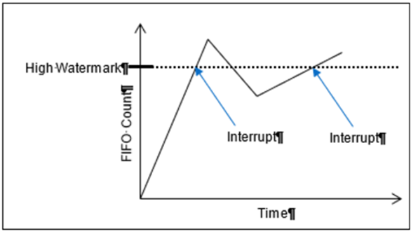
| FIFO Set Edge/Level Interrupt | |
| Function: | When the FIFO Status Interrupt Enable register is enabled, this register determines whether the interrupt will be generated for either “sense on edge” or “sense on level” event detection. |
| Read/Write: | R/W |
| Initialized Value: | 0 |
| Operational Settings: | Write a 1 to sense on level and a 0 to sense on edge. |
Function Register Map
| Input |
| Output |
| RECEIVE REGISTERS | |||||
| OFFSET | REGISTER NAME | ACCESS | OFFSET | REGISTER NAME | ACCESS |
| 0x1004 | Receive FIFO Buffer Data Ch 1 | R-H, W-A | 0x1008 | Receive FIFO Word Count Ch 1 | R |
| 0x1084 | Receive FIFO Buffer Data Ch 2 | R-H, W-A | 0x1088 | Receive FIFO Word Count Ch 2 | R |
| 0x1104 | Receive FIFO Buffer Data Ch 3 | R-H, W-A | 0x1108 | Receive FIFO Word Count Ch 3 | R |
| 0x1184 | Receive FIFO Buffer Data Ch 4 | R-H, W-A | 0x1188 | Receive FIFO Word Count Ch 4 | R |
| NOTE: For Receive FIFO Buffer Data, 'H' is 'Host; 'A' is 'ARM'. | |||||
| 0x100C | Receive FIFO Frame Count Ch 1 | R | |||
| 0x108C | Receive FIFO Frame Count Ch 2 | R | |||
| 0x110C | Receive FIFO Frame Count Ch 3 | R | |||
| 0x118C | Receive FIFO Frame Count Ch 4 | R | |||
| TRANSMIT REGISTERS | |||||
| OFFSET | REGISTER NAME | ACCESS | OFFSET | REGISTER NAME | ACCESS |
| 0x1010 | Transmit FIFO Buffer Data Ch 1 | W-H, R-A | 0x1014 | Transmit FIFO Word Count Ch 1 | R |
| 0x1090 | Transmit FIFO Buffer Data Ch 2 | W-H, R-A | 0x1094 | Transmit FIFO Word Count Ch 2 | R |
| 0x1110 | Transmit FIFO Buffer Data Ch 3 | W-H, R-A | 0x1114 | Transmit FIFO Word Count Ch 3 | R |
| 0x1190 | Transmit FIFO Buffer Data Ch 4 | W-H, R-A | 0x1194 | Transmit FIFO Word Count Ch 4 | R |
| NOTE: For Transmit FIFO Buffer Data, 'H' is 'Host; 'A' is 'ARM'. | |||||
| 0x1018 | Transmit FIFO Frame Count Ch 1 | R | |||
| 0x1098 | Transmit FIFO Frame Count Ch 2 | R | |||
| 0x1118 | Transmit FIFO Frame Count Ch 3 | R | |||
| 0x1198 | Transmit FIFO Frame Count Ch 4 | R | |||
| COMMAND REGISTERS | |||||
| OFFSET | REGISTER NAME | ACCESS | OFFSET | REGISTER NAME | ACCESS |
| 0x1400 | BM Capabilities Register | R/W | |||
| 0x1028 | Command FIFO Buffer Data Ch 1 | W-H, R-A | 0x102C | Command FIFO Word Count Ch 1 | R |
| 0x10A8 | Command FIFO Buffer Data Ch 2 | W-H, R-A | 0x10AC | Command FIFO Word Count Ch 2 | R |
| 0x1128 | Command FIFO Buffer Data Ch 3 | W-H, R-A | 0x112C | Command FIFO Word Count Ch 3 | R |
| 0x11A8 | Command FIFO Buffer Data Ch 4 | W-H, R-A | 0x11AC | Command FIFO Word Count Ch 4 | R |
| NOTE: For Command FIFO Buffer Data, 'H' is 'Host; 'A' is 'ARM'. | |||||
| CONTROL REGISTERS | |||||
| OFFSET | REGISTER NAME | ACCESS | OFFSET | REGISTER NAME | ACCESS |
| 0x1000 | Control Ch 1 | R/W | 0x101C | Data Rate/Base Rate Ch 1 | R/W |
| 0x1080 | Control Ch 2 | R/W | 0x109C | Data Rate/Base Rate Ch 2 | R/W |
| 0x1100 | Control Ch 3 | R/W | 0x111C | Data Rate/Base Rate Ch 3 | R/W |
| 0x1180 | Control Ch 4 | R/W | 0x119C | Data Rate/Base Rate Ch 4 | R/W |
| 0x1020 | Sample Point Ch 1 | R/W | 0x1060 | RxMaxWorkMS Ch 1 | R/W |
| 0x10A0 | Sample Point Ch 2 | R/W | 0x10E0 | RxMaxWorkMS Ch 2 | R/W |
| 0x1120 | Sample Point Ch 3 | R/W | 0x1160 | RxMaxWorkMS Ch 3 | R/W |
| 0x11A0 | Sample Point Ch 4 | R/W | 0x11E0 | RxMaxWorkMS Ch 4 | R/W |
| 0x1064 | TxMaxWorkMS Ch 1 | R/W | |||
| 0x10E4 | TxMaxWorkMS Ch 2 | R/W | |||
| 0x1164 | TxMaxWorkMS Ch 3 | R/W | |||
| 0x11E4 | TxMaxWorkMS Ch 4 | R/W | |||
| MESSAGE STATUS/MONITOR REGISTERS | |||||
| OFFSET | REGISTER NAME | ACCESS | OFFSET | REGISTER NAME | ACCESS |
| 0x1024 | Last Error Code Ch 1 | R/W | |||
| 0x10A4 | Last Error Code Ch 2 | R/W | |||
| 0x1124 | Last Error Code Ch 3 | R/W | |||
| 0x11A4 | Last Error Code Ch 4 | R/W | |||
| 0x1050 | Drop Count Ch 1 | R/W | 0x1030 | Tx/Rx Error Counter Ch 1 | R/W |
| 0x10D0 | Drop Count Ch 2 | R/W | 0x10B0 | Tx/Rx Error Counter Ch 2 | R/W |
| 0x1150 | Drop Count Ch 3 | R/W | 0x1130 | Tx/Rx Error Counter Ch 3 | R/W |
| 0x11D0 | Drop Count Ch 4 | R/W | 0x11B0 | Tx/Rx Error Counter Ch 4 | R/W |
| BIT REGISTER | |||||
| *When an event is detected, the bit associated with the event is set in this register and will remain set until the user clears the event bit. Clearing the bit requires writing a 1 back to the specific bit that was set when read (i.e. write-1-to-clear, writing a '1' to a bit set to '1' will set the bit to '0'). | |||||
| OFFSET | REGISTER NAME | ACCESS | OFFSET | REGISTER NAME | ACCESS |
| 0x0800 | BIT Dynamic Status | R | |||
| 0x0804 | BIT Latched Status* | R/W | |||
| 0x0808 | BIT Interrupt Enable | R/W | |||
| 0x080C | BIT Set Edge/Level Interrupt | R/W | |||
| FIFO STATUS REGISTERS | |||||
| *When an event is detected, the bit associated with the event is set in this register and will remain set until the user clears the event bit. Clearing the bit requires writing a 1 back to the specific bit that was set when read (i.e. write-1-to-clear, writing a '1' to a bit set to '1' will set the bit to '0'). | |||||
| OFFSET | REGISTER NAME | ACCESS | OFFSET | REGISTER NAME | ACCESS |
| 0x0810 | Dynamic Status Ch 1 | R | 0x0820 | Dynamic Status Ch 2 | R |
| 0x0814 | Latched Status Ch 1* | R/W | 0x0824 | Latched Status Ch 2* | R/W |
| 0x0818 | Interrupt Enable Ch 1 | R/W | 0x0828 | Interrupt Enable Ch 2 | R/W |
| 0x081C | Set Edge/Level Interrupt Ch 1 | R/W | 0x082C | Set Edge/Level Interrupt Ch 2 | R/W |
| 0x0830 | Dynamic Status Ch 3 | R | 0x0840 | Dynamic Status Ch 4 | R |
| 0x0834 | Latched Status Ch 3* | R/W | 0x0844 | Latched Status Ch 4* | R/W |
| 0x0838 | Interrupt Enable Ch 3 | R/W | 0x0848 | Interrupt Enable Ch 4 | R/W |
| 0x083C | Set Edge/Level Interrupt Ch 3 | R/W | 0x084C | Set Edge/Level Interrupt Ch 4 | R/W |
| CHANNEL STATUS REGISTER | |||||
| *When an event is detected, the bit associated with the event is set in this register and will remain set until the user clears the event bit. Clearing the bit requires writing a 1 back to the specific bit that was set when read (i.e. write-1-to-clear, writing a '1' to a bit set to '1' will set the bit to '0'). | |||||
| OFFSET | REGISTER NAME | ACCESS | OFFSET | REGISTER NAME | ACCESS |
| 0x0920 | Dynamic Status Ch 1-4 | R | |||
| 0x0924 | Latched Status Ch 1-4* | R/W | |||
| 0x0928 | Interrupt Enable Ch 1-4 | R/W | |||
| 0x92C | Set Edge/Level Interrupt Ch 1-4 | R/W | |||
| RESPONSE REGISTERS | |||||
| When data other than CAN messages needs to be returned from the CAN module, the data to be returned is placed in a series of Response Registers. Each channel has its own series of Response Registers that can be used. The BareMetal logic will fill these registers and update the Response Count so the consumer can determine how many of the Response Registers need to be read. | |||||
| OFFSET | REGISTER NAME | ACCESS | OFFSET | REGISTER NAME | ACCESS |
| 0x1300 | Response Count Ch 1 | R | 0x1380 | Response Count Ch 2 | R |
| 0x1304 | Response Data Ch 1 | R | 0x1384 | Response Data Ch 2 | R |
| 0x1308 | Response Data Ch 1 | R | 0x1388 | Response Data Ch 2 | R |
| 0x130C | Response Data Ch 1 | R | 0x138C | Response Data Ch 2 | R |
| ... | ... | ||||
| 0x137C | Response Data Ch 1 | R | 0x13FC | Response Data Ch 2 | R |
| 0x1400 | Response Count Ch 3 | R | 0x1480 | Response Count Ch 4 | R |
| 0x1404 | Response Data Ch 3 | R | 0x1484 | Response Data Ch 4 | R |
| 0x1408 | Response Data Ch 3 | R | 0x1488 | Response Data Ch 4 | R |
| 0x140C | Response Data Ch 3 | R | 0x148C | Response Data Ch 4 | R |
| ... | ... | ||||
| 0x147C | Response Data Ch 3 | R | 0x14FC | Response Data Ch 4 | R |
Discrete Input/Output Function
Principle of Operation
The onboard Discrete Input/Output communications function provides up to 24 individual digital I/O channels with BIT fault detection (DT1/DT4 module-type), which enables flagging of non-compliant outputs or inconsistent input readings between dual input measurements.
When channels are programmed as inputs, they can be used for either voltage or contact sensing. Channels set for contact sensing (e.g. sensing a relay contact position; OPEN-CLOSED) can be configured with a programmable “pull-up” or “pull-down” (current source or sink) which effectively provides the proper voltage level change to sense the open state of the contact. This unique design eliminates the need for external resistors or mechanical jumpers. Instead, this design offers a current source/sink (in banks of 6 channels) that the user programs to a desired current (0-5 mA) level.
When programmed as outputs, each channel can be set for high-side (current-source), low-side (current-sink) or push-pull (current-source-sink) operation. The load impedance determines the delivered switched output current drive - up to 500 mA per channel. Diode clamping is provided (useful for inductive loads, such as relays) and thermal protection.
Overcurrent protection is implemented using current sensing technology. When the current exceeds a programmed threshold of 650 mA steady-state, or a higher short duration, the overcurrent/short-circuit protection is triggered, shutting down the output drivers for safety. The overcurrent fault status will be indicated for the affected channels and will require a reset operation to restore output. To reset this condition, a reset command needs to be issued to the Overcurrent Reset register, which will restore drive output and allow the latched status to be reset. This is separate from the reset for the Overcurrent Interrupt Enable register on this module. It is recommended that a reset command is done whenever status is cleared to avoid a non-apparent output reset condition.
The 24 channels are configured as 4 banks of 6 channels. Each bank is provided with a separate external input VCC and a ground return (GND) pin. The GND pins are common within the module but are isolated from system (power) GND.
Operational requirements/assumptions:
- An external source VCC supply must be wired for proper:
- Output operation as a current source
- Input operation when requiring a programmed pull-up current (i.e. programmed “pull-up” for input contact sense; OPEN/GND detect/state change).
- An external source Ground/Return must be wired for all I/O configurations. The Ground/Return must be the input signal or the load current sink ground/reference.
Input/Output Interface
Each channel can be configured as an input or one of three types of outputs.
Output
When configured as an output, the interface can act as a “High-Side”, “Low-Side” or “Push-Pull” drive, providing up to 500 mA per channel or 1 A when two channels are connected in parallel. The total output per module is 8 A (2 A per bank).
Note
Maximum source current ‘rules’ for rear I/O connectors still apply - see specifications.
Input
When configured as an input, output drivers are disabled. The I/O interface can act as a constant current source, current sink or voltage sensing circuit. For contact sensing, each channel may be set for pull-up or pull-down using the Select Pull Up or Pull Down register and by entering the appropriate current level in the Pull-Up/Down Current register. Contact closure and hysteresis may be defined using the Upper Voltage and Lower Voltage Threshold registers. No additional resistors or hardware are required to provide for current flow. A current value of zero disables the current source/sink circuits and configures the module for voltage sensing. Default is voltage sensing. Level or contact sensing can be mixed within a channel bank if the contact sensing channels are externally pulled up or pulled down.
Note
If this module supplies the current for the contact sensing, then level and contact sensing cannot be mixed within a channel bank. All four threshold levels must be programmed in monotonic, increasing order of: Minimum Low, Lower, Upper and Maximum High. For input and output, threshold levels define logic state. For output, threshold levels are used in BIT test (wrap-around) signal monitoring. A pair of drive FETs and current circuits are provided at each I/O pin. See the functional representation of the drivers in the I/O Circuits interface diagram below.
Input/Output Circuits
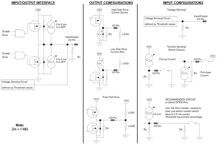
Discrete I/O Threshold Programming
Four threshold levels: Max High Voltage Threshold, Upper Voltage Threshold, Lower Voltage Threshold, and Min Low Voltage Threshold offer maximum user flexibility. All four threshold levels must be programmed. For input or output, the threshold levels will define the logic states. For proper operation, the threshold values should be programmed such that:
Max High Voltage Threshold > Upper Voltage Threshold > Lower Voltage Threshold > Min Low Voltage Threshold
Program Upper and Lower Voltage Thresholds, keeping the 0.25 V min. differential in mind, and then add debounce time as required. When the input signal exceeds the Upper Voltage Threshold, a logic high 1 is maintained until the input signal falls below the Lower Voltage Threshold. Conversely, when the input signal falls below the Lower Voltage Threshold, a logic low 0.
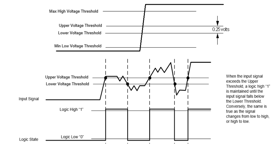
Debounce Programming
The Debounce register, when programmed for a non-zero value, is used with channels programmed as input to “filter” or “ignore” expected application spurious initial transitions. Once a signal level is a logic voltage level period longer than the Debounce Time (Logic High and Logic Low), a logic transition is validated. Signal pulse widths less than programmed Debounce Time are filtered. Once valid, the transition status register flag is set for the channel and the output logic changes state.
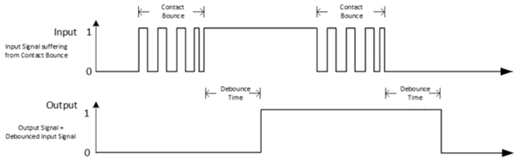
Automatic Background Built-In Test (BIT)/Diagnostic Capability
The onboard Discrete Input/Output function supports automatic background BIT testing that verifies channel processing. The testing is totally transparent to the user, requires no external programming and has no effect on the operation of the module. This capability is accomplished by an additional test comparator that is incorporated into each module. The test comparator checks each channel and is compared against the operational channel. Depending upon the configuration, the Input data read, or Output logic written of the operational channel and test comparator must agree or a fault is indicated with the results available in the associated status register. The results of the tests are stored in the BIT Dynamic Status and BIT Latched Status registers.
The technique used by the continuous background BIT (CBIT) test consists of an “add-2, subtract-1” counting scheme. The BIT counter is incremented by 2 when a BIT-fault is detected and decremented by 1 when there is no BIT fault detected and the BIT counter is greater than 0. When the BIT counter exceeds the (programmed) Background BIT Threshold value, the specific channel’s fault bit in the BIT status register will be set. Note, the interval at which BIT is performed is dependent and differs between module types. Rather than specifying the BIT Threshold as a “count”, the BIT Threshold is specified as a time in milliseconds. The module will convert the time specified to the BIT Threshold “count” based on the BIT interval for that module. The “add-2, subtract-1” counting scheme effectively filters momentary or intermittent anomalies by allowing them to “come and go“ before a BIT fault status or indication is flagged (e.g. BIT faults would register when sustained; i.e. at a ten second interval, not a 10-millisecond interval). This prevents spurious faults from registering valid such as those caused by EMI and/or dirty power causing false BIT faults. Putting more “weight” on errors (“add-2”) and less “weight” on subsequent passing results (subtract-1) will result in a BIT failure indication even if a channel “oscillates” between a pass and fail state.
In addition to BIT, the onboard Discrete Input/Output function tests for overcurrent conditions and provides Above Max High Voltage, Below Min Low Voltage, and Mid-Range Voltage statuses for threshold signal transitioning.
Status and Interrupts
The onboard Discrete Input/Output provide registers that indicate faults or events. Refer to ‘Appendix B: Onboard Module Status and Interrupts’ for the Principle of Operation description.
Unit Conversions
The Discrete I/O Threshold and Measurement registers can be programmed to be utilized as a single precision floating point value (IEEE-754) or as a 32-bit integer value. The purpose for providing this feature is to offload the processing that is normally performed by the mission processor to convert the integer values to floating-point values.
When the Enable Floating Point Mode register is set to 1 (Floating Point Mode) the following registers are formatted as Single Precision Floating Point Value (IEEE-754):
- Voltage Reading (Volts)
- Current Reading (mA)
- VCC Voltage Reading (Volts)
- Max High Voltage Threshold (Volts)*
- Upper Voltage Threshold (Volts)*
- Lower Voltage Threshold (Volts)*
- Min Low Voltage Threshold (Volts)*
- Pull-Up/Down Current (mA)*
*When the Enable Floating Point Mode register is set to 1, it is important that these registers are updated with the Single Precision Floating Point (IEEE-754) representation of the value for proper operation of the channel. Conversely, when the Enable Floating Point Mode register is set to 0, these registers must be updated with the Integer 32-bit representation of the value.
Note
when changing the Enable Floating Point Mode from Integer Mode to Floating Point Mode or vice versa, the following step should be followed to avoid faults from falsely being generated because data registers (such as Thresholds) or internal registers may have the incorrect binary representation of the values:
- Set the Enable Floating Point Mode register to the desired mode (Integer = 0 or Floating Point = 1).
- Wait for the Floating Point State register to match the value for the requested Floating Point Mode (Integer = 0, Floating Point = 1); this indicates that the module’s conversion of the register values and internal values is complete. Data registers will be converted to the units specified and can be read in that specified format.
- Initialize configuration and control registers with the values in the units specified (Integer or Floating Point).
User Watchdog Timer Capability
The onboard Discrete Input/Output Option provide registers that support User Watchdog Timer capability. Refer to ‘Appendix C: Onboard Discrete I/O User Watchdog Timer Functionality’ for the Principle of Operation description.
Enhanced Functionality Option
The onboard Discrete Input/Output Option offers a separate option for enhanced input and output mode functionality. For incoming signals (inputs), the enhanced modes include Pulse Measurements, Transition Timestamps, Transition Counters, Period Measurement and Frequency Measurement. For outputs, the enhanced modes include PWM (Pulse Width Modulation) Outputs and Pattern Generator Outputs.
Refer to ‘Appendix D: Onboard Discrete I/O Enhanced Input/Output Functionality’ for the Principle of Operation description.
Register Descriptions
The register descriptions provide the Register Name, Type, Data Range, Read or Write information, power on default initialized values, a description of the function and a data table where applicable.
Discrete Input/Output Registers
Each channel can be configured as an input or one of three types of outputs. The I/O Format (Ch1-16 and Ch17-24) registers are used to set each channel’s Input/Output configuration. The Write Outputs register controls the output channels to either a High (1) or Low (0) state, and the Read I/O register contains the discrete channel’s state (High (1) or Low (0)) as specified by the channel’s threshold configurations.
| I/O Format Ch1-16 | |
| Function: | Sets channels 1-16 as inputs or outputs. See I/O Format Ch17-24 register for channels 17-24. |
| Type: | unsigned binary word (32-bit) |
| Data Range: | 0x0000 0000 to 0xFFFF FFFF |
| Read/Write: | R/W |
| Initialized Value: | 0 |
| Operational Settings: | Write integer 0 for input; 1, 2, or 3 for specific output format. |
| Integer | DH | DL | (2 bits per channel) |
| 0 | 0 | 0 | Input |
| 1 | 0 | 1 | Output, Low-side switched, with/without current pull up |
| 2 | 1 | 0 | Output, High-side switched, with/without current pull down |
| 3 | 1 | 1 | Output, push-pull |
| D31 | D30 | D29 | D28 | D27 | D26 | D25 | D24 | D23 | D22 | D21 | D20 | D19 | D18 | D17 | D16 |
| Ch16 | Ch15 | Ch14 | Ch13 | Ch12 | Ch11 | Ch10 | Ch9 | ||||||||
| D15 | D14 | D13 | D12 | D11 | D10 | D9 | D8 | D7 | D6 | D5 | D4 | D3 | D2 | D1 | D0 |
| Ch8 | Ch7 | Ch6 | Ch5 | Ch4 | Ch3 | Ch2 | Ch1 | ||||||||
| I/O Format Ch17-24 | |
| Function: | Sets channels 17-24 as inputs or outputs. See I/O Format Ch1-16 for channels 1-16. |
| Type: | unsigned binary word (32-bit) |
| Data Range: | 0x0000 0000 to 0x0000 FFFF |
| Read/Write: | R/W |
| Initialized Value: | 0 |
| Operational Settings: | Write integer 0 for input; 1, 2, or 3 for specific output format. |
| Integer | DH | DL | (2 bits per channel) |
| 0 | 0 | 0 | Input |
| 1 | 0 | 1 | Output, Low-side switched, with/without current pull up |
| 2 | 1 | 0 | Output, High-side switched, with/without current pull down |
| 3 | 1 | 1 | Output, push-pull |
| D31 | D30 | D29 | D28 | D27 | D26 | D25 | D24 | D23 | D22 | D21 | D20 | D19 | D18 | D17 | D16 |
| 0 | 0 | 0 | 0 | 0 | 0 | 0 | 0 | 0 | 0 | 0 | 0 | 0 | 0 | 0 | 0 |
| D15 | D14 | D13 | D12 | D11 | D10 | D9 | D8 | D7 | D6 | D5 | D4 | D3 | D2 | D1 | D0 |
| Ch24 | Ch23 | Ch22 | Ch21 | Ch20 | Ch19 | Ch18 | Ch17 | ||||||||
| Write Outputs | |
| Function: | Drives output channels High 1 or Low 0 |
| Type: | unsigned binary word (32-bit) |
| Data Range: | 0x0000 0000 to 0x00FF FFFF |
| Read/Write: | R/W |
| Initialized Value: | 0 |
| Operational Settings: | Write 1 to drive output high. Write 0 to drive output low. |
| D31 | D30 | D29 | D28 | D27 | D26 | D25 | D24 | D23 | D22 | D21 | D20 | D19 | D18 | D17 | D16 |
| 0 | 0 | 0 | 0 | 0 | 0 | 0 | 0 | Ch24 | Ch23 | Ch22 | Ch21 | Ch20 | Ch19 | Ch18 | Ch17 |
| D15 | D14 | D13 | D12 | D11 | D10 | D9 | D8 | D7 | D6 | D5 | D4 | D3 | D2 | D1 | D0 |
| Ch16 | Ch15 | Ch14 | Ch13 | Ch12 | Ch11 | Ch10 | Ch9 | Ch8 | Ch7 | Ch6 | Ch5 | Ch4 | Ch3 | Ch2 | Ch1 |
| Input/Output State | |
| Function: | Reads High 1 or Low 0 inputs or outputs as defined by internal channel threshold values. |
| Type: | unsigned binary word (32-bit) |
| Data Range: | 0x0000 0000 to 0x00FF FFFF |
| Read/Write: | R |
| Initialized Value: | N/A |
| Operational Settings: | Bit-mapped per channel. |
| D31 | D30 | D29 | D28 | D27 | D26 | D25 | D24 | D23 | D22 | D21 | D20 | D19 | D18 | D17 | D16 |
| 0 | 0 | 0 | 0 | 0 | 0 | 0 | 0 | Ch24 | Ch23 | Ch22 | Ch21 | Ch20 | Ch19 | Ch18 | Ch17 |
| D15 | D14 | D13 | D12 | D11 | D10 | D9 | D8 | D7 | D6 | D5 | D4 | D3 | D2 | D1 | D0 |
| Ch16 | Ch15 | Ch14 | Ch13 | Ch12 | Ch11 | Ch10 | Ch9 | Ch8 | Ch7 | Ch6 | Ch5 | Ch4 | Ch3 | Ch2 | Ch1 |
Discrete Input/Output Threshold Programming Registers
Four threshold levels: Max High Threshold, Upper Threshold, Lower Threshold, and Min Low Threshold are programmable for each Discrete channel in the module.
| Max High Voltage Threshold (Enable Floating Point Mode: Integer Mode) | |||||||||||||||
| Upper Voltage Threshold (Enable Floating Point Mode: Integer Mode) | |||||||||||||||
| Lower Voltage Threshold (Enable Floating Point Mode: Integer Mode) | |||||||||||||||
| Min Low Voltage Threshold (Enable Floating Point Mode: Integer Mode) | |||||||||||||||
| D31 | D30 | D29 | D28 | D27 | D26 | D25 | D24 | D23 | D22 | D21 | D20 | D19 | D18 | D17 | D16 |
| 0 | 0 | 0 | 0 | 0 | 0 | 0 | 0 | 0 | 0 | 0 | 0 | 0 | 0 | 0 | 0 |
| D15 | D14 | D13 | D12 | D11 | D10 | D9 | D8 | D7 | D6 | D5 | D4 | D3 | D2 | D1 | D0 |
| 0 | 0 | 0 | D | D | D | D | D | D | D | D | D | D | D | D | D |
| Max High Voltage Threshold (Enable Floating Point Mode: Floating Point Mode) | |||||||||||||||
| Upper Voltage Threshold (Enable Floating Point Mode: Floating Point Mode) | |||||||||||||||
| Lower Voltage Threshold (Enable Floating Point Mode: Floating Point Mode) | |||||||||||||||
| Min Low Voltage Threshold (Enable Floating Point Mode: Floating Point Mode) | |||||||||||||||
| D31 | D30 | D29 | D28 | D27 | D26 | D25 | D24 | D23 | D22 | D21 | D20 | D19 | D18 | D17 | D16 |
| D | D | D | D | D | D | D | D | D | D | D | D | D | D | D | D |
| D15 | D14 | D13 | D12 | D11 | D10 | D9 | D8 | D7 | D6 | D5 | D4 | D3 | D2 | D1 | D0 |
| D | D | D | D | D | D | D | D | D | D | D | D | D | D | D | D |
| Max High Voltage Threshold | |
| Function: | Sets the maximum high voltage threshold value. Programmable per channel from + 0 VDC to 60 VDC. |
| Type: | unsigned binary word (32-bit) (Integer Mode) or Single Precision Floating Point Value (IEEE-754) (Floating Point Mode) |
| Data Range: | Enable Floating Point Mode: 0 (Integer Mode) 0x0000 0000 to 0x0000 0258 Enable Floating Point Mode: 1 (Floating Point Mode) Single Precision Floating Point Value (IEEE-754) |
| Read/Write: | R/W |
| Initialized Value: | 0x32 |
| Operational Settings: | Assumes that the programmed level is the minimum voltage used to indicate a Max High Voltage Threshold. If a signal is greater than the Max High Threshold value, a flag is set in the Max High Voltage Threshold Status register. The Max High Voltage Threshold register may be used to monitor any type of high signal voltage condition or threshold such as a “Short to V” as it applies to input measurement as well as contact sensing applications. Integer Mode: LSB is 0.1 VDC. For example: to program 5.0 VDC, 5.0 / 0.1 = 50 (binary equivalent for 50 is 0x0000 0032). Floating Point Mode: Set Max High Voltage Threshold value as a Single Precision Floating Point Value (IEEE-754). For example, to program 5.0 V, enter 5.0 as a single precision floating point value (IEEE-754) (binary equivalent 5.0 is 0x40A0 0000). |
| Upper Voltage Threshold | |
| Function: | Sets the upper voltage threshold value. Programmable per channel from + 0 VDC to 60 VDC. |
| Type: | unsigned binary word (32-bit) (Integer Mode) or Single Precision Floating Point Value (IEEE-754) (Floating Point Mode) |
| Data Range: | Enable Floating Point Mode: 0 (Integer Mode) 0x0000 0000 to 0x0000 0258 Enable Floating Point Mode: 1 (Floating Point Mode) Single Precision Floating Point Value (IEEE-754) |
| Read/Write: | R/W |
| Initialized Value: | 0x28 |
| Operational Settings: | A signal is considered logic High 1 when its value exceeds the Upper Voltage Threshold and does not consequently fall below the Upper Voltage Threshold in less than the programmed Debounce Time. Integer Mode: LSB is 0.1 VDC. For example: to program 3.5 VDC, 3.5 / 0.1 = 35 (binary equivalent for 35 is 0x0000 0023). Floating Point Mode: Set Upper Voltage Threshold value as a Single Precision Floating Point Value (IEEE-754). For example, to program 3.5 V, enter 3.5 as a single precision floating point value (IEEE-754) (binary equivalent 3.5 is 0x4060 0000). |
| Lower Voltage Threshold | |
| Function: | Sets the lower voltage threshold value. Programmable per channel from + 0 VDC to 60 VDC. |
| Type: | unsigned binary word (32-bit) (Integer Mode) or Single Precision Floating Point Value (IEEE-754) (Floating Point Mode) |
| Data Range: | Enable Floating Point Mode: 0 (Integer Mode) 0x0000 0000 to 0x0000 0258 Enable Floating Point Mode: 1 (Floating Point Mode) Single Precision Floating Point Value (IEEE-754) |
| Read/Write: | R/W |
| Initialized Value: | 0x10 |
| Operational Settings: | A signal is considered logic Low 0 when its value falls below the Lower Voltage Threshold and does not consequently rise above the Lower Voltage Threshold in less than the programmed Debounce Time. Integer Mode: LSB is 0.1 VDC. For example: to program 1.5 VDC, 1.5 / 0.1 = 15 (binary equivalent for 15 is 0x0000 000F). Floating Point Mode: Set Lower Voltage Threshold value as a Single Precision Floating Point Value (IEEE-754). For example, to program 1.5 V, enter 1.5 as a single precision floating point value (IEEE-754) (binary equivalent 1.5 is 0x3FC0 0000). |
| Min Low Voltage Threshold | |
| Function: | Sets the minimum low voltage threshold. Programmable per channel + 0 VDC to 60 VDC. |
| Type: | unsigned binary word (32-bit) (Integer Mode) or Single Precision Floating Point Value (IEEE-754) (Floating Point Mode) |
| Data Range: | Enable Floating Point Mode: 0 (Integer Mode) 0x0000 0000 to 0x0000 0258 Enable Floating Point Mode: 1 (Floating Point Mode) Single Precision Floating Point Value (IEEE-754) |
| Read/Write: | R/W |
| Initialized Value: | 0xA |
| Operational Settings: | Assumes that the programmed level is the voltage used to indicate a minimum low threshold. If a signal is less than the Min Low Voltage Threshold value, a flag is set in the Min Low Voltage Threshold Status register. The Min Low VoltageThreshold register may be used to monitor any type of low signal voltage condition or threshold such as a “Short to Ground” as it applies to input measurement as well as contact sensing applications. Integer Mode: LSB is 0.1 VDC. For example: to program 0.5 VDC, 0.5 / 0.1 = 5 (binary equivalent for 5 is 0x0000 0005). Floating Point Mode: Set Min Low VoltageThreshold value as a Single Precision Floating Point Value (IEEE-754). For example, to program 0.5 V, enter 0.5 as a single precision floating point value (IEEE-754) (binary equivalent 0.5 is 0x3F00 0000). |
Discrete Input/Output Measurement Registers
The measured voltage at the I/O pin for each channel can be read from the Voltage Reading register.
| Voltage Reading | |
| Function: | Reads actual voltage at I/O pin per individual channel. |
| Type: | unsigned binary word (32-bit) (Integer Mode) or Single Precision Floating Point Value (IEEE-754) (Floating Point Mode) |
| Data Range: | Enable Floating Point Mode: 0 (Integer Mode) 0x0000 0000 to 0x0000 0258 Enable Floating Point Mode: 1 (Floating Point Mode) Single Precision Floating Point Value (IEEE-754) |
| Read/Write: | R |
| Initialized Value: | N/A |
| Operational Settings: | Integer Mode: LSB is 0.1 VDC. If the register value is 261 (binary equivalent for 261 is 0x0000 0105), conversion to the voltage value is 261 * 0.1 = 26.1 V. Floating Point Mode: Read as a Single Precision Floating Point Value (IEEE-754). For example, if the register value is 0x41D0 CCCD, this is equivalent to is 26.1, which represent 26.1 V. |
| Voltage Reading (Enable Floating Point Mode: Integer Mode) | |||||||||||||||
| D31 | D30 | D29 | D28 | D27 | D26 | D25 | D24 | D23 | D22 | D21 | D20 | D19 | D18 | D17 | D16 |
| 0 | 0 | 0 | 0 | 0 | 0 | 0 | 0 | 0 | 0 | 0 | 0 | 0 | 0 | 0 | 0 |
| D15 | D14 | D13 | D12 | D11 | D10 | D9 | D8 | D7 | D6 | D5 | D4 | D3 | D2 | D1 | D0 |
| 0 | 0 | 0 | D | D | D | D | D | D | D | D | D | D | D | D | D |
| Voltage Reading (Enable Floating Point Mode: Floating Point Mode) | |||||||||||||||
| D31 | D30 | D29 | D28 | D27 | D26 | D25 | D24 | D23 | D22 | D21 | D20 | D19 | D18 | D17 | D16 |
| D | D | D | D | D | D | D | D | D | D | D | D | D | D | D | D |
| D15 | D14 | D13 | D12 | D11 | D10 | D9 | D8 | D7 | D6 | D5 | D4 | D3 | D2 | D1 | D0 |
| D | D | D | D | D | D | D | D | D | D | D | D | D | D | D | D |
| Current Reading | |
| Function: | Reads actual output current through I/O pin per channel. |
| Type: | signed binary word (32-bit (only lower 16-bit is used)) (Integer Mode) or Single Precision Floating Point Value (IEEE-754) (Floating Point Mode) |
| Data Range: | Enable Floating Point Mode: 0 (Integer Mode) (2's compliment. 16-bit value sign extended to 32 bits) 0x0000 0000 to 0x0000 00D0 (positive) or 0x0000 FF30 (negative) Enable Floating Point Mode: 1 (Floating Point Mode) Single Precision Floating Point Value (IEEE-754) |
| Read/Write: | R |
| Initialized Value: | N/A |
| Operational Settings: | Integer Mode: LSB is 3.0 mA. Value is signed binary 16-bit word. Read as 2's complement value for positive and negative current readings. For example, if the register value is 50 (binary equivalent for 50 is 0x0000 0032), the conversion to the current value is 50 * 3.0 = 150 mA. If register value is -50 (binary equivalent for -150 is 0x0000 FFCE), the conversion to the current value is -50 * 3.0 = -150 mA. Floating Point Mode: Read as a Single Precision Floating Point Value (IEEE-754). The value will represent a positive or negative current reading. For example, if the register value is 0x4316 0000, this is equivalent to 150, which represent 150 mA. If the register value is 0xC316 0000, this is equivalent to -150, which represents -150 mA. |
| Current Reading (Enable Floating Point Mode: Integer Mode) | |||||||||||||||
| D31 | D30 | D29 | D28 | D27 | D26 | D25 | D24 | D23 | D22 | D21 | D20 | D19 | D18 | D17 | D16 |
| 0 | 0 | 0 | 0 | 0 | 0 | 0 | 0 | 0 | 0 | 0 | 0 | 0 | 0 | 0 | 0 |
| D15 | D14 | D13 | D12 | D11 | D10 | D9 | D8 | D7 | D6 | D5 | D4 | D3 | D2 | D1 | D0 |
| D | D | D | D | D | D | D | D | D | D | D | D | D | D | D | D |
| Current Reading (Enable Floating Point Mode: Floating Point Mode) | |||||||||||||||
| D31 | D30 | D29 | D28 | D27 | D26 | D25 | D24 | D23 | D22 | D21 | D20 | D19 | D18 | D17 | D16 |
| D | D | D | D | D | D | D | D | D | D | D | D | D | D | D | D |
| D15 | D14 | D13 | D12 | D11 | D10 | D9 | D8 | D7 | D6 | D5 | D4 | D3 | D2 | D1 | D0 |
| D | D | D | D | D | D | D | D | D | D | D | D | D | D | D | D |
VCC Bank Registers
There are four VCC banks where each bank controls 6 discrete channels. Configuration for each bank involves specifying if the bank is configured for pull-up or pull-down and the current for source/sink. The measured voltage for VCC can be read from the VCC Voltage Reading register.
| Select Pull-Up or Pull-Down | |
| Function: | Configures Pull-up or Pull-down configuration per 6-channel bank |
| Type: | unsigned binary word (32-bit) |
| Data Range: | 0 to 0x0000 000F |
| Read/Write: | R/W |
| Initialized Value: | 0 |
| Operational Settings: | Set bit to 1 to configure channel bank to Pull-up. Set bit to 0 to configure channel bank to Pull-down. Each data bit configures entire bank of 6 channels. |
Note
For contact (switch closure) applications, a current supply (Vcc) is required for internal pull-up.
| Bit(s) | Name | Description |
| D31:D4 | Reserved | Set Reserved bits to 0. |
| D3 | Configure Bank 4 (Ch 19-24) | 1=Pull-Up, 0=Pull-Down |
| D2 | Configure Bank 3 (Ch 13-18) | 1=Pull-Up, 0=Pull-Down |
| D1 | Configure Bank 2 (Ch 07-12) | 1=Pull-Up, 0=Pull-Down |
| D0 | Configure Bank 1 (Ch 01-06) | 1=Pull-Up, 0=Pull-Down |
| Pull-Up/Down Current | |
| Function: | Sets current for source/sink per 6-channel bank. Programmable from 0 to 5 mA. |
| Type: | unsigned binary word (32-bit) (Integer Mode) or Single Precision Floating Point Value (IEEE-754) (Floating Point Mode) |
| Data Range: | Enable Floating Point Mode: 0 (Integer Mode) 0x0000 0000 to 0x0000 0032 Enable Floating Point Mode: 1 (Floating Point Mode) Floating Point Value (IEEE-754) |
| Read/Write: | R/W |
| Initialized Value: | 0 (Voltage Sensing) |
| Operational Settings: | A current of zero disables the current source/sink circuits and configures for voltage sensing (refer to Input in Input/Output Interface section). Integer Mode: LSB is 0.1 mA. For example: to program 5 mA, 5 / 0.1 = 50 (binary equivalent for 50 is 0x0000 0032). Floating Point Mode: Set the current for source/sink as a Single Precision Floating Point Value (IEEE-754). For example, to program 5 mA, enter 5.0 as a Single Precision Floating Point Value (IEEE-754) (binary equivalent for 5.0 is 0x40A0 0000). |
| Pull-Up/Down Current (Enable Floating Point Mode: Integer Mode) | |||||||||||||||
| D31 | D30 | D29 | D28 | D27 | D26 | D25 | D24 | D23 | D22 | D21 | D20 | D19 | D18 | D17 | D16 |
| 0 | 0 | 0 | 0 | 0 | 0 | 0 | 0 | 0 | 0 | 0 | 0 | 0 | 0 | 0 | 0 |
| D15 | D14 | D13 | D12 | D11 | D10 | D9 | D8 | D7 | D6 | D5 | D4 | D3 | D2 | D1 | D0 |
| 0 | 0 | 0 | 0 | 0 | 0 | 0 | 0 | 0 | 0 | D | D | D | D | D | D |
| Pull-Up/Down Current (Enable Floating Point Mode: Floating Point Mode) | |||||||||||||||
| D31 | D30 | D29 | D28 | D27 | D26 | D25 | D24 | D23 | D22 | D21 | D20 | D19 | D18 | D17 | D16 |
| D | D | D | D | D | D | D | D | D | D | D | D | D | D | D | D |
| D15 | D14 | D13 | D12 | D11 | D10 | D9 | D8 | D7 | D6 | D5 | D4 | D3 | D2 | D1 | D0 |
| D | D | D | D | D | D | D | D | D | D | D | D | D | D | D | D |
| VCC Voltage Reading | |
| Function: | Read the VCC bank voltage. |
| Type: | unsigned binary word (32-bit) (Integer Mode) or Single Precision Floating Point Value (IEEE-754) (Floating Point Mode) |
| Data Range: | Enable Floating Point Mode: 0 (Integer Mode) 0x0000 0000 to 0x0000 0258 Enable Floating Point Mode: 1 (Floating Point Mode) Single Precision Floating Point Value (IEEE-754) |
| Read/Write: | R |
| Initialized Value: | N/A |
| Operational Settings: | Integer Mode: LSB is 0.1 VDC. If the register value is 260 (binary equivalent for this value is 0x0000 0104), conversion to the voltage value is 260 * 0.1 = 26.0 V. Floating Point Mode: Read as a Single Precision Floating Point Value (IEEE-754). For example, the binary equivalent for 0x41D0 0000 is 26.0 which represent 26.0 V. |
| VCC Voltage Reading (Enable Floating Point Mode: Integer Mode) | |||||||||||||||
| D31 | D30 | D29 | D28 | D27 | D26 | D25 | D24 | D23 | D22 | D21 | D20 | D19 | D18 | D17 | D16 |
| 0 | 0 | 0 | 0 | 0 | 0 | 0 | 0 | 0 | 0 | 0 | 0 | 0 | 0 | 0 | 0 |
| D15 | D14 | D13 | D12 | D11 | D10 | D9 | D8 | D7 | D6 | D5 | D4 | D3 | D2 | D1 | D0 |
| 0 | 0 | 0 | D | D | D | D | D | D | D | D | D | D | D | D | D |
| VCC Voltage Reading (Enable Floating Point Mode: Floating Point Mode) | |||||||||||||||
| D31 | D30 | D29 | D28 | D27 | D26 | D25 | D24 | D23 | D22 | D21 | D20 | D19 | D18 | D17 | D16 |
| D | D | D | D | D | D | D | D | D | D | D | D | D | D | D | D |
| D15 | D14 | D13 | D12 | D11 | D10 | D9 | D8 | D7 | D6 | D5 | D4 | D3 | D2 | D1 | D0 |
| D | D | D | D | D | D | D | D | D | D | D | D | D | D | D | D |
Discrete Input/Output Control Registers
Control of the Discrete I/O channels include specifying the Debounce time for each input channel and resetting the I/O channel on an overcurrent condition.
| Debounce Time | |
| Function: | When set for inputs, the input signal will have the debounce filtering applied based on this programmed value. This is selectable for each channel. |
| Type: | unsigned binary word (32-bit) |
| Data Range: | 0x0000 0000 to 0xFFFF FFFF |
| Read/Write: | R/W |
| Initialized Value: | 0 |
| Operational Settings: | The Debounce Time register, when programmed for a non-zero value, is used with channels programmed as input to “filter” or “ignore” expected application spurious initial transitions. Enter required Debounce Time into appropriate channel registers. LSB weight is 10 µs/bit (register may be programmed from 0x0000 0000 (debounce filter inactive) through a maximum of 0xFFFF FFFF (2^32 * 10µs). (full scale w/ 10 µs resolution). Once a signal level is a logic voltage level period longer than the debounce time (Logic High and Logic Low), a logic transition is validated. Signal pulse widths less than programmed Debounce Time are filtered. Once valid, the transition status register flag is set for the channel and the output logic changes state. Enter a value of 0 to disable debounce filtering. |
| Overcurrent Reset | |
| Function: | Resets disabled channels in Overcurrent Latched Status register following an overcurrent condition as measured by the Current Reading register. |
| Type: | unsigned binary word (32-bit) |
| Data Range: | 0x0000 0000 to 0x00FF FFFF |
| Read/Write: | R/W |
| Initialized Value: | 0 |
| Operational Settings: | 1 is written to reset disabled channels. Processor will write a 0 back to the Overcurrent Reset register when reset process is complete. |
| D31 | D30 | D29 | D28 | D27 | D26 | D25 | D24 | D23 | D22 | D21 | D20 | D19 | D18 | D17 | D16 |
| 0 | 0 | 0 | 0 | 0 | 0 | 0 | 0 | Ch24 | Ch23 | Ch22 | Ch21 | Ch20 | Ch19 | Ch18 | Ch17 |
| D15 | D14 | D13 | D12 | D11 | D10 | D9 | D8 | D7 | D6 | D5 | D4 | D3 | D2 | D1 | D0 |
| Ch16 | Ch15 | Ch14 | Ch13 | Ch12 | Ch11 | Ch10 | Ch9 | Ch8 | Ch7 | Ch6 | Ch5 | Ch4 | Ch3 | Ch2 | Ch1 |
Unit Conversion Programming Registers
The Enable Floating Point register provides the ability to set the Threshold values as floating-point values and read the Voltage Reading registers as floating-point values. The purpose for this feature is to offload the processing that is normally performed by the mission processor to convert the integer values to floating-point values.
| Enable Floating Point Mode | |
| Function: | Sets all channels for floating point mode or integer module. |
| Type: | unsigned binary word (32-bit) |
| Data Range: | 0 to 1 |
| Read/Write: | R/W |
| Initialized Value: | 0 |
| Operational Settings: | Set bit to 1 to enable Floating Point Mode and 0 for Integer Mode. Wait for the Floating Point State register to match the value for the requested Floating Point Mode (Integer = 0, Floating Point = 1); this indicates that the module's conversion of the register values and internal values is complete before changing the values of the configuration and control registers with the values in the units specified (Integer or Floating Point). |
| D31 | D30 | D29 | D28 | D27 | D26 | D25 | D24 | D23 | D22 | D21 | D20 | D19 | D18 | D17 | D16 |
| 0 | 0 | 0 | 0 | 0 | 0 | 0 | 0 | 0 | 0 | 0 | 0 | 0 | 0 | 0 | 0 |
| D15 | D14 | D13 | D12 | D11 | D10 | D9 | D8 | D7 | D6 | D5 | D4 | D3 | D2 | D1 | D0 |
| 0 | 0 | 0 | 0 | 0 | 0 | 0 | 0 | 0 | 0 | 0 | 0 | 0 | 0 | 0 | D |
| Floating Point State | |
| Function: | Indicates the state of the mode selected (Integer or Floating Point). |
| Type: | unsigned binary word (32-bit) |
| Data Range: | 0 to 1 |
| Read/Write: | R |
| Initialized Value: | 0 |
| Operational Settings: | Indicates the whether the module registers are in Integer (0) or Floating Point Mode (1). When the Enable Floating Point Mode is modified, the application must wait until this register's value matches the requested mode before changing the values of the configuration and control registers with the values in the units specified (Integer or Floating Point). |
| D31 | D30 | D29 | D28 | D27 | D26 | D25 | D24 | D23 | D22 | D21 | D20 | D19 | D18 | D17 | D16 |
| 0 | 0 | 0 | 0 | 0 | 0 | 0 | 0 | 0 | 0 | 0 | 0 | 0 | 0 | 0 | 0 |
| D15 | D14 | D13 | D12 | D11 | D10 | D9 | D8 | D7 | D6 | D5 | D4 | D3 | D2 | D1 | D0 |
| 0 | 0 | 0 | 0 | 0 | 0 | 0 | 0 | 0 | 0 | 0 | 0 | 0 | 0 | 0 | D |
Background BIT Threshold Programming Registers
The Background BIT Threshold register provides the ability to specify the minimum time before the BIT fault is reported in the BIT Status registers. The Reset BIT register provides the ability to reset the BIT counter used in CBIT.
| Background BIT Threshold | |
| Function: | Sets BIT Threshold value (in milliseconds) to use for all channels for BIT failure indication. |
| Type: | unsigned binary word (32-bit) |
| Data Range: | 1 ms to 232 ms |
| Read/Write: | R/W |
| Initialized Value: | 5 (5 ms) |
| Operational Settings: | The interval at which BIT is performed is dependent and differs between module types. Rather than specifying the BIT Threshold as a “count”, the BIT Threshold is specified as a time in milliseconds. The module will convert the time specified to the BIT Threshold “count” based on the BIT interval for that module. |
| BIT Count Clear | |
| Function: | Resets the CBIT internal circuitry and count mechanism. Set the bit corresponding to the channel you want to clear. |
| Type: | unsigned binary word (32-bit) |
| Data Range: | 0x0000 0000 to 0x00FF FFFF |
| Read/Write: | W |
| Initialized Value: | 0 |
| Operational Settings: | Set bit to 1 for channel to resets the CBIT mechanisms. Bit is self-clearing. |
| D31 | D30 | D29 | D28 | D27 | D26 | D25 | D24 | D23 | D22 | D21 | D20 | D19 | D18 | D17 | D16 |
| 0 | 0 | 0 | 0 | 0 | 0 | 0 | 0 | Ch24 | Ch23 | Ch22 | Ch21 | Ch20 | Ch19 | Ch18 | Ch17 |
| D15 | D14 | D13 | D12 | D11 | D10 | D9 | D8 | D7 | D6 | D5 | D4 | D3 | D2 | D1 | D0 |
| Ch16 | Ch15 | Ch14 | Ch13 | Ch12 | Ch11 | Ch10 | Ch9 | Ch8 | Ch7 | Ch6 | Ch5 | Ch4 | Ch3 | Ch2 | Ch1 |
User Watchdog Timer Programming Registers
Refer to ‘Appendix C: Onboard Discrete I/O User Watchdog Timer Functionality’ for the Register descriptions.
Status and Interrupt Registers
The Discrete Module provides status registers for BIT, Low-to-High Transition, High-to-Low Transition, Above Max High Voltage, Below Min Low Voltage, and Mid-Range Voltage.
| Channel Status Enable | |
| Function: | Determines whether to update the status for the channels. This feature can be used to “mask” status bits of unused channels in status registers that are bitmapped by channel. |
| Type: | unsigned binary word (32-bit) |
| Data Range: | 0x0000 0000 to 0x00FF FFFF (Channel Status) |
| Read/Write: | R/W |
| Initialized Value: | 0x0000 0FFF |
| Operational Settings: | When the bit corresponding to a given channel in the Channel Status Enable register is not enabled (0) the status will be masked and report “0” or “no failure”. This applies to all statuses that are bitmapped by channel (BIT Status, Low-to-High Transition Status, High-to-Low Transition Status, Overcurrent Status, Above Max High Voltage Status, Below Min Low Voltage Status, Mid-Range Voltage and Summary Status). |
Note
Background BIT will continue to run even if the Channel Status Enable is set to 0.
| D31 | D30 | D29 | D28 | D27 | D26 | D25 | D24 | D23 | D22 | D21 | D20 | D19 | D18 | D17 | D16 |
| 0 | 0 | 0 | 0 | 0 | 0 | 0 | 0 | Ch24 | Ch23 | Ch22 | Ch21 | Ch20 | Ch19 | Ch18 | Ch17 |
| D15 | D14 | D13 | D12 | D11 | D10 | D9 | D8 | D7 | D6 | D5 | D4 | D3 | D2 | D1 | D0 |
| Ch16 | Ch15 | Ch14 | Ch13 | Ch12 | Ch11 | Ch10 | Ch9 | Ch8 | Ch7 | Ch6 | Ch5 | Ch4 | Ch3 | Ch2 | Ch1 |
BIT Status
There are four registers associated with the BIT Status: Dynamic, Latched, Interrupt Enable, and Set Edge/Level Interrupt.
Note
When a BIT fault is detected, reading the Voltage Reading Error and the Driver Error register will provide additional diagnostics on the cause of the BIT fault.
| BIT Status | |
| Function: | Sets the corresponding bit associated with the channel's BIT error. |
| Type: | unsigned binary word (32-bit) |
| Data Range: | 0x0000 0000 to 0x00FF FFFF |
| Read/Write: | R (Dynamic), R/W (Latched, Interrupt Enable, Edge/Level Interrupt) |
| Initialized Value: | 0 |
Note
Faults are detected (associated channel(s) bit set to 1 within 10 ms.
| BIT Dynamic Status | |||||||||||||||
| BIT Latched Status | |||||||||||||||
| BIT Interrupt Enable | |||||||||||||||
| BIT Set Edge/Level Interrupt | |||||||||||||||
| D31 | D30 | D29 | D28 | D27 | D26 | D25 | D24 | D23 | D22 | D21 | D20 | D19 | D18 | D17 | D16 |
| 0 | 0 | 0 | 0 | 0 | 0 | 0 | 0 | Ch24 | Ch23 | Ch22 | Ch21 | Ch20 | Ch19 | Ch18 | Ch17 |
| D15 | D14 | D13 | D12 | D11 | D10 | D9 | D8 | D7 | D6 | D5 | D4 | D3 | D2 | D1 | D0 |
| Ch16 | Ch15 | Ch14 | Ch13 | Ch12 | Ch11 | Ch10 | Ch9 | Ch8 | Ch7 | Ch6 | Ch5 | Ch4 | Ch3 | Ch2 | Ch1 |
| Voltage Reading Error | |
| Function: | The Voltage Reading Error register is set when a redundant voltage measurement is inconsistent with the input voltage level detected. |
| Type: | unsigned binary word (32-bit) |
| Data Range: | 0x0000 0000 to 0x00FF FFFF |
| Read/Write: | R |
| Initialized Value: | 0 |
| Operational Settings: | 1 is read when a fault is detected. 0 indicates no fault detected. |
Note
Faults are detected (associated channel(s) bit set to 1 within 10 ms.
Note
Clearing the latched BIT status will also clear this error register.
| D31 | D30 | D29 | D28 | D27 | D26 | D25 | D24 | D23 | D22 | D21 | D20 | D19 | D18 | D17 | D16 |
| 0 | 0 | 0 | 0 | 0 | 0 | 0 | 0 | Ch24 | Ch23 | Ch22 | Ch21 | Ch20 | Ch19 | Ch18 | Ch17 |
| D15 | D14 | D13 | D12 | D11 | D10 | D9 | D8 | D7 | D6 | D5 | D4 | D3 | D2 | D1 | D0 |
| Ch16 | Ch15 | Ch14 | Ch13 | Ch12 | Ch11 | Ch10 | Ch9 | Ch8 | Ch7 | Ch6 | Ch5 | Ch4 | Ch3 | Ch2 | Ch1 |
| Driver Error | |
| Function: | The Driver Error register is set when the voltage reading mismatches active driver measurement and is inconsistent with the input driver level detected (Note: requires programming of thresholds). |
| Type: | unsigned binary word (32-bit) |
| Data Range: | 0x0000 0000 to 0x00FF FFFF |
| Read/Write: | R |
| Initialized Value: | 0 |
| Operational Settings: | 1 is read when a fault is detected. 0 indicates no fault detected. |
Note
Faults are detected (associated channel(s) bit set to 1 within 10 ms.
Note
Clearing the latched BIT status will also clear this error register.
| D31 | D30 | D29 | D28 | D27 | D26 | D25 | D24 | D23 | D22 | D21 | D20 | D19 | D18 | D17 | D16 |
| 0 | 0 | 0 | 0 | 0 | 0 | 0 | 0 | Ch24 | Ch23 | Ch22 | Ch21 | Ch20 | Ch19 | Ch18 | Ch17 |
| D15 | D14 | D13 | D12 | D11 | D10 | D9 | D8 | D7 | D6 | D5 | D4 | D3 | D2 | D1 | D0 |
| Ch16 | Ch15 | Ch14 | Ch13 | Ch12 | Ch11 | Ch10 | Ch9 | Ch8 | Ch7 | Ch6 | Ch5 | Ch4 | Ch3 | Ch2 | Ch1 |
Low-to-High Transition Status
There are four registers associated with the Low-to-High Transition Status: Dynamic, Latched, Interrupt Enable, and Set Edge/Level Interrupt.
| Low-to-High Transition Status | |
| Function: | Sets the corresponding bit associated with the channel's Low-to-High Transition event. |
| Type: | unsigned binary word (32-bit) |
| Data Range: | 0x0000 0000 to 0x00FF FFFF |
| Read/Write: | R (Dynamic), R/W (Latched, Interrupt Enable, Edge/Level Interrupt) |
| Initialized Value: | 0 |
Note
Considered “momentary” during the actual event when detected. Programmable for level or edge sensing, status is indicated (associated channel(s) bit set to 1 within 20 µs.
Note
Programmable for level or edge sensing, status is indicated (associated channel(s) bit set to 1 within 20 µs.
Note
Transition status follows the value read by the Input/Output State register.
| Low-to-High Dynamic Status | |||||||||||||||
| Low-to-High Latched Status | |||||||||||||||
| Low-to-High Interrupt Enable | |||||||||||||||
| Low-to-High Set Edge/Level Interrupt | |||||||||||||||
| D31 | D30 | D29 | D28 | D27 | D26 | D25 | D24 | D23 | D22 | D21 | D20 | D19 | D18 | D17 | D16 |
| 0 | 0 | 0 | 0 | 0 | 0 | 0 | 0 | Ch24 | Ch23 | Ch22 | Ch21 | Ch20 | Ch19 | Ch18 | Ch17 |
| D15 | D14 | D13 | D12 | D11 | D10 | D9 | D8 | D7 | D6 | D5 | D4 | D3 | D2 | D1 | D0 |
| Ch16 | Ch15 | Ch14 | Ch13 | Ch12 | Ch11 | Ch10 | Ch9 | Ch8 | Ch7 | Ch6 | Ch5 | Ch4 | Ch3 | Ch2 | Ch1 |
High-to-Low Transition Status
There are four registers associated with the High-to-Low Transition Status: Dynamic, Latched, Interrupt Enable, and Set Edge/Level Interrupt.
| High-to-Low Transition Status | |
| Function: | Sets the corresponding bit associated with the channel's High-to-Low Transition event. |
| Type: | unsigned binary word (32-bit) |
| Data Range: | 0x0000 0000 to 0x00FF FFFF |
| Read/Write: | R (Dynamic), R/W (Latched, Interrupt Enable, Edge/Level Interrupt) |
| Initialized Value: | 0 |
Note
Considered “momentary” during the actual event when detected. Programmable for level or edge sensing, status is indicated (associated channel(s) bit set to 1 within 20 µs.
Note
Programmable for level or edge sensing, status is indicated (associated channel(s) bit set to 1 within 20 µs.
Note
Transition status follows the value read by the Input/Output State register.
| High-to-Low Dynamic Status | |||||||||||||||
| High-to-Low Latched Status | |||||||||||||||
| High-to-Low Interrupt Enable | |||||||||||||||
| High-to-Low Set Edge/Level Interrupt | |||||||||||||||
| D31 | D30 | D29 | D28 | D27 | D26 | D25 | D24 | D23 | D22 | D21 | D20 | D19 | D18 | D17 | D16 |
| 0 | 0 | 0 | 0 | 0 | 0 | 0 | 0 | Ch24 | Ch23 | Ch22 | Ch21 | Ch20 | Ch19 | Ch18 | Ch17 |
| D15 | D14 | D13 | D12 | D11 | D10 | D9 | D8 | D7 | D6 | D5 | D4 | D3 | D2 | D1 | D0 |
| Ch16 | Ch15 | Ch14 | Ch13 | Ch12 | Ch11 | Ch10 | Ch9 | Ch8 | Ch7 | Ch6 | Ch5 | Ch4 | Ch3 | Ch2 | Ch1 |
Overcurrent Status
There are four registers associated with the Overcurrent Status: Dynamic, Latched, Interrupt Enable, and Set Edge/Level Interrupt.
| Overcurrent Status | |
| Function: | Sets the corresponding bit associated with the channel's Overcurrent error. |
| Type: | unsigned binary word (32-bit) |
| Data Range: | 0x0000 0000 to 0x00FF FFFF |
| Read/Write: | R (Dynamic), R/W (Latched, Interrupt Enable, Edge/Level Interrupt) |
| Initialized Value: | 0 |
Note
Status is indicated (associated channel(s) bit set to 1, within 80 ms.
Note
Latched Status is indicated (associated channel(s) bit set to 1, within 80 ms.
Note
Channel(s) shut down by overcurrent sensed can be reset by writing to the Overcurrent Clear register.
| Overcurrent Dynamic Status | |||||||||||||||
| Overcurrent Latched Status | |||||||||||||||
| Overcurrent Interrupt Enable | |||||||||||||||
| Overcurrent Set Edge/Level Interrupt | |||||||||||||||
| D31 | D30 | D29 | D28 | D27 | D26 | D25 | D24 | D23 | D22 | D21 | D20 | D19 | D18 | D17 | D16 |
| 0 | 0 | 0 | 0 | 0 | 0 | 0 | 0 | Ch24 | Ch23 | Ch22 | Ch21 | Ch20 | Ch19 | Ch18 | Ch17 |
| D15 | D14 | D13 | D12 | D11 | D10 | D9 | D8 | D7 | D6 | D5 | D4 | D3 | D2 | D1 | D0 |
| Ch16 | Ch15 | Ch14 | Ch13 | Ch12 | Ch11 | Ch10 | Ch9 | Ch8 | Ch7 | Ch6 | Ch5 | Ch4 | Ch3 | Ch2 | Ch1 |
Above Max High Voltage Status
There are four registers associated with the Above Max High Voltage Status: Dynamic, Latched, Interrupt Enable, and Set Edge/Level Interrupt. Latched status is indicated (bit is set) within 500 µs. Write a 1 to clear status.
| Above Max High Voltage Status | |
| Function: | Sets the corresponding bit associated with the channel's Above Max High Voltage event. |
| Type: | unsigned binary word (32-bit) |
| Data Range: | 0x0000 0000 to 0x00FF FFFF |
| Read/Write: | R (Dynamic), R/W (Latched, Interrupt Enable, Edge/Level Interrupt) |
| Initialized Value: | 0 |
| Above Max High Voltage Dynamic Status | |||||||||||||||
| Above Max High Voltage Latched Status | |||||||||||||||
| Above Max High Voltage Interrupt Enable | |||||||||||||||
| Above Max High Voltage Set Edge/Level Interrupt | |||||||||||||||
| D31 | D30 | D29 | D28 | D27 | D26 | D25 | D24 | D23 | D22 | D21 | D20 | D19 | D18 | D17 | D16 |
| 0 | 0 | 0 | 0 | 0 | 0 | 0 | 0 | Ch24 | Ch23 | Ch22 | Ch21 | Ch20 | Ch19 | Ch18 | Ch17 |
| D15 | D14 | D13 | D12 | D11 | D10 | D9 | D8 | D7 | D6 | D5 | D4 | D3 | D2 | D1 | D0 |
| Ch16 | Ch15 | Ch14 | Ch13 | Ch12 | Ch11 | Ch10 | Ch9 | Ch8 | Ch7 | Ch6 | Ch5 | Ch4 | Ch3 | Ch2 | Ch1 |
Below Min Low Voltage Status
There are four registers associated with the Below Min Low Voltage Status: Dynamic, Latched, Interrupt Enable, and Set Edge/Level Interrupt. Latched status is indicated (bit is set) within 500 µs. Write a 1 to clear status.
| Below Min Low Voltage Status | |
| Function: | Sets the corresponding bit associated with the channel's Below Min Low Voltage event. |
| Type: | unsigned binary word (32-bit) |
| Data Range: | 0x0000 0000 to 0x00FF FFFF |
| Read/Write: | R (Dynamic), R/W (Latched, Interrupt Enable, Edge/Level Interrupt) |
| Initialized Value: | 0 |
| Below Min Low Voltage Dynamic Status | |||||||||||||||
| Below Min Low Voltage Latched Status | |||||||||||||||
| Below Min Low Voltage Interrupt Enable | |||||||||||||||
| Below Min Low Voltage Set Edge/Level Interrupt | |||||||||||||||
| D31 | D30 | D29 | D28 | D27 | D26 | D25 | D24 | D23 | D22 | D21 | D20 | D19 | D18 | D17 | D16 |
| 0 | 0 | 0 | 0 | 0 | 0 | 0 | 0 | Ch24 | Ch23 | Ch22 | Ch21 | Ch20 | Ch19 | Ch18 | Ch17 |
| D15 | D14 | D13 | D12 | D11 | D10 | D9 | D8 | D7 | D6 | D5 | D4 | D3 | D2 | D1 | D0 |
| Ch16 | Ch15 | Ch14 | Ch13 | Ch12 | Ch11 | Ch10 | Ch9 | Ch8 | Ch7 | Ch6 | Ch5 | Ch4 | Ch3 | Ch2 | Ch1 |
Mid-Range Voltage Status
There are four registers associated with the Mid-Range Voltage Status: Dynamic, Latched, Interrupt Enable, and Set Edge/Level Interrupt. Latched status is indicated (bit is set) within 500 µs. Write a 1 to clear status.
| Mid-Range Voltage Status | |
| Function: | Sets the corresponding bit associated with the channel's Mid-Range Voltage event. |
| Type: | unsigned binary word (32-bit) |
| Data Range: | 0x0000 0000 to 0x00FF FFFF |
| Read/Write: | R (Dynamic), R/W (Latched, Interrupt Enable, Edge/Level Interrupt) |
| Initialized Value: | 0 |
Note
Voltage level needs to be between the upper and lower thresholds for the debounce time for this status to assert.
Note
In the event this status is asserted, the Input/Output state will hold its previous state.
| Mid-Range Voltage Dynamic Status | |||||||||||||||
| Mid-Range Voltage Latched Status | |||||||||||||||
| Mid-Range Voltage Interrupt Enable | |||||||||||||||
| Mid-Range Set Voltage Edge/Level Interrupt | |||||||||||||||
| D31 | D30 | D29 | D28 | D27 | D26 | D25 | D24 | D23 | D22 | D21 | D20 | D19 | D18 | D17 | D16 |
| 0 | 0 | 0 | 0 | 0 | 0 | 0 | 0 | Ch24 | Ch23 | Ch22 | Ch21 | Ch20 | Ch19 | Ch18 | Ch17 |
| D15 | D14 | D13 | D12 | D11 | D10 | D9 | D8 | D7 | D6 | D5 | D4 | D3 | D2 | D1 | D0 |
| Ch16 | Ch15 | Ch14 | Ch13 | Ch12 | Ch11 | Ch10 | Ch9 | Ch8 | Ch7 | Ch6 | Ch5 | Ch4 | Ch3 | Ch2 | Ch1 |
User Watchdog Timer Fault Status
The onboard Discrete Input/Output option provide registers that support User Watchdog Timer capability. Refer to ‘Appendix C: Onboard Discrete I/O User Watchdog Timer Functionality’ for the Onboard Discrete I/O User Watchdog Timer Fault Status Register descriptions.
Summary Status
There are four registers associated with the Summary Status: Dynamic, Latched, Interrupt Enable, and Set Edge/Level Interrupt.
| Summary Status | |
| Function: | Sets the corresponding bit if any fault (BIT and Overcurrent) occurs on that channel. |
| Type: | unsigned binary word (32-bit) |
| Data Range: | 0x0000 0000 to 0x00FF FFFF |
| Read/Write: | R (Dynamic), R/W (Latched, Interrupt Enable, Edge/Level Interrupt) |
| Initialized Value: | 0 |
| Summary Status Dynamic Status | |||||||||||||||
| Summary Status Latched Status | |||||||||||||||
| Summary Status Interrupt Enable | |||||||||||||||
| Summary Status Set Edge/Level Interrupt | |||||||||||||||
| D31 | D30 | D29 | D28 | D27 | D26 | D25 | D24 | D23 | D22 | D21 | D20 | D19 | D18 | D17 | D16 |
| 0 | 0 | 0 | 0 | 0 | 0 | 0 | 0 | Ch24 | Ch23 | Ch22 | Ch21 | Ch20 | Ch19 | Ch18 | Ch17 |
| D15 | D14 | D13 | D12 | D11 | D10 | D9 | D8 | D7 | D6 | D5 | D4 | D3 | D2 | D1 | D0 |
| Ch16 | Ch15 | Ch14 | Ch13 | Ch12 | Ch11 | Ch10 | Ch9 | Ch8 | Ch7 | Ch6 | Ch5 | Ch4 | Ch3 | Ch2 | Ch1 |
Enhanced Functionality Option Registers
Refer to ‘Appendix D: Onboard Discrete I/O Enhanced Input/Output Functionality’ for the Register descriptions.
Function Register Map
KEY
| Configuration/Control |
| Measurement/Status |
| DISCRETE INPUT/OUTPUT REGISTERS | |||||
| NOTE: Base Address - 0x9010 C000 | |||||
| OFFSET | REGISTER NAME | ACCESS | OFFSET | REGISTER NAME | ACCESS |
| 0x1038 | I/O Format Ch1-12 | R/W | 0x1000 | I/O State | R |
| 0x103C | I/O Format Ch17-24 | R/W | 0x1024 | Write Outputs | R/W |
| DISCRETE INPUT/OUTPUT THRESHOLD PROGRAMMING REGISTERS | |||||
| **Data is represented in Floating Point if Enable Floating Point Mode register is set to Floating Point Mode (1). | |||||
| OFFSET | REGISTER NAME | ACCESS | OFFSET | REGISTER NAME | ACCESS |
| 0x20C0 | Max High Voltage Threshold Ch 1** | R/W | 0x20C4 | Upper Voltage Threshold Ch 1** | R/W |
| 0x2140 | Max High Voltage Threshold Ch 2** | R/W | 0x2144 | Upper Voltage Threshold Ch 2** | R/W |
| 0x21C0 | Max High Voltage Threshold Ch 3** | R/W | 0x21C4 | Upper Voltage Threshold Ch 3** | R/W |
| 0x2240 | Max High Voltage Threshold Ch 4** | R/W | 0x2244 | Upper Voltage Threshold Ch 4** | R/W |
| 0x22C0 | Max High Voltage Threshold Ch 5** | R/W | 0x22C4 | Upper Voltage Threshold Ch 5** | R/W |
| 0x2340 | Max High Voltage Threshold Ch 6** | R/W | 0x2344 | Upper Voltage Threshold Ch 6** | R/W |
| 0x23C0 | Max High Voltage Threshold Ch 7** | R/W | 0x23C4 | Upper Voltage Threshold Ch 7** | R/W |
| 0x2440 | Max High Voltage Threshold Ch 8** | R/W | 0x2444 | Upper Voltage Threshold Ch 8** | R/W |
| 0x24C0 | Max High Voltage Threshold Ch 9** | R/W | 0x24C4 | Upper Voltage Threshold Ch 9** | R/W |
| 0x2540 | Max High Voltage Threshold Ch 10** | R/W | 0x2544 | Upper Voltage Threshold Ch 10** | R/W |
| 0x25C0 | Max High Voltage Threshold Ch 11** | R/W | 0x25C4 | Upper Voltage Threshold Ch 11** | R/W |
| 0x2640 | Max High Voltage Threshold Ch 12** | R/W | 0x2644 | Upper Voltage Threshold Ch 12** | R/W |
| 0x26C0 | Max High Voltage Threshold Ch 13** | R/W | 0x26C4 | Upper Voltage Threshold Ch 13** | R/W |
| 0x2740 | Max High Voltage Threshold Ch 14** | R/W | 0x2744 | Upper Voltage Threshold Ch 14** | R/W |
| 0x27C0 | Max High Voltage Threshold Ch 15** | R/W | 0x27C4 | Upper Voltage Threshold Ch 15** | R/W |
| 0x2840 | Max High Voltage Threshold Ch 16** | R/W | 0x2844 | Upper Voltage Threshold Ch 16** | R/W |
| 0x28C0 | Max High Voltage Threshold Ch 17** | R/W | 0x28C4 | Upper Voltage Threshold Ch 17** | R/W |
| 0x2940 | Max High Voltage Threshold Ch 18** | R/W | 0x2944 | Upper Voltage Threshold Ch 18** | R/W |
| 0x29C0 | Max High Voltage Threshold Ch 19** | R/W | 0x29C4 | Upper Voltage Threshold Ch 19** | R/W |
| 0x2A40 | Max High Voltage Threshold Ch 20** | R/W | 0x2A44 | Upper Voltage Threshold Ch 20** | R/W |
| 0x2AC0 | Max High Voltage Threshold Ch 21** | R/W | 0x2AC4 | Upper Voltage Threshold Ch 21** | R/W |
| 0x2B40 | Max High Voltage Threshold Ch 22** | R/W | 0x2B44 | Upper Voltage Threshold Ch 22** | R/W |
| 0x2BC0 | Max High Voltage Threshold Ch 23** | R/W | 0x2BC4 | Upper Voltage Threshold Ch 23** | R/W |
| 0x2C40 | Max High Voltage Threshold Ch 24** | R/W | 0x2C44 | Upper Voltage Threshold Ch 24** | R/W |
| 0x20C8 | Lower Voltage Threshold Ch 1** | R/W | 0x20CC | Min Low Voltage Threshold Ch 1** | R/W |
| 0x2148 | Lower Voltage Threshold Ch 2** | R/W | 0x214C | Min Low Voltage Threshold Ch 2** | R/W |
| 0x21C8 | Lower Voltage Threshold Ch 3** | R/W | 0x21CC | Min Low Voltage Threshold Ch 3** | R/W |
| 0x2248 | Lower Voltage Threshold Ch 4** | R/W | 0x224C | Min Low Voltage Threshold Ch 4** | R/W |
| 0x22C8 | Lower Voltage Threshold Ch 5** | R/W | 0x22CC | Min Low Voltage Threshold Ch 5** | R/W |
| 0x2348 | Lower Voltage Threshold Ch 6** | R/W | 0x234C | Min Low Voltage Threshold Ch 6** | R/W |
| 0x23C8 | Lower Voltage Threshold Ch 7** | R/W | 0x23CC | Min Low Voltage Threshold Ch 7** | R/W |
| 0x2448 | Lower Voltage Threshold Ch 8** | R/W | 0x244C | Min Low Voltage Threshold Ch 8** | R/W |
| 0x24C8 | Lower Voltage Threshold Ch 9** | R/W | 0x24CC | Min Low Voltage Threshold Ch 9** | R/W |
| 0x2548 | Lower Voltage Threshold Ch 10** | R/W | 0x254C | Min Low Voltage Threshold Ch 10** | R/W |
| 0x25C8 | Lower Voltage Threshold Ch 11** | R/W | 0x25CC | Min Low Voltage Threshold Ch 11** | R/W |
| 0x2648 | Lower Voltage Threshold Ch 12** | R/W | 0x264C | Min Low Voltage Threshold Ch 12** | R/W |
| 0x26C8 | Lower Voltage Threshold Ch 13** | R/W | 0x26CC | Min Low Voltage Threshold Ch 13** | R/W |
| 0x2748 | Lower Voltage Threshold Ch 14** | R/W | 0x274C | Min Low Voltage Threshold Ch 14** | R/W |
| 0x27C8 | Lower Voltage Threshold Ch 15** | R/W | 0x27CC | Min Low Voltage Threshold Ch 15** | R/W |
| 0x2848 | Lower Voltage Threshold Ch 16** | R/W | 0x284C | Min Low Voltage Threshold Ch 16** | R/W |
| 0x28C8 | Lower Voltage Threshold Ch 17** | R/W | 0x28CC | Min Low Voltage Threshold Ch 17** | R/W |
| 0x2948 | Lower Voltage Threshold Ch 18** | R/W | 0x294C | Min Low Voltage Threshold Ch 18** | R/W |
| 0x29C8 | Lower Voltage Threshold Ch 19** | R/W | 0x29CC | Min Low Voltage Threshold Ch 19** | R/W |
| 0x2A48 | Lower Voltage Threshold Ch 20** | R/W | 0x2A4C | Min Low Voltage Threshold Ch 20** | R/W |
| 0x2AC8 | Lower Voltage Threshold Ch 21** | R/W | 0x2ACC | Min Low Voltage Threshold Ch 21** | R/W |
| 0x2B48 | Lower Voltage Threshold Ch 22** | R/W | 0x2B4C | Min Low Voltage Threshold Ch 22** | R/W |
| 0x2BC8 | Lower Voltage Threshold Ch 23** | R/W | 0x2BCC | Min Low Voltage Threshold Ch 23** | R/W |
| 0x2C48 | Lower Voltage Threshold Ch 24** | R/W | 0x2C4C | Min Low Voltage Threshold Ch 24** | R/W |
| DISCRETE INPUT/OUTPUT MEASUREMENT REGISTERS | |||||
| **Data is represented in Floating Point if Enable Floating Point Mode register is set to Floating Point Mode (1). | |||||
| OFFSET | REGISTER NAME | ACCESS | OFFSET | REGISTER NAME | ACCESS |
| 0x20E0 | Voltage Reading Ch 1** | R | 0x20E4 | Current Reading Ch 1** | R |
| 0x2160 | Voltage Reading Ch 2** | R | 0x2164 | Current Reading Ch 2** | R |
| 0x21E0 | Voltage Reading Ch 3** | R | 0x21E4 | Current Reading Ch 3** | R |
| 0x2260 | Voltage Reading Ch 4** | R | 0x2264 | Current Reading Ch 4** | R |
| 0x22E0 | Voltage Reading Ch 5** | R | 0x22E4 | Current Reading Ch 5** | R |
| 0x2360 | Voltage Reading Ch 6** | R | 0x2364 | Current Reading Ch 6** | R |
| 0x23E0 | Voltage Reading Ch 7** | R | 0x23E4 | Current Reading Ch 7** | R |
| 0x2460 | Voltage Reading Ch 8** | R | 0x2464 | Current Reading Ch 8** | R |
| 0x24E0 | Voltage Reading Ch 9** | R | 0x24E4 | Current Reading Ch 9** | R |
| 0x2560 | Voltage Reading Ch 10** | R | 0x2564 | Current Reading Ch 10** | R |
| 0x25E0 | Voltage Reading Ch 11** | R | 0x25E4 | Current Reading Ch 11** | R |
| 0x2660 | Voltage Reading Ch 12** | R | 0x2664 | Current Reading Ch 12** | R |
| 0x26E0 | Voltage Reading Ch 13** | R | 0x26E4 | Current Reading Ch 13** | R |
| 0x2760 | Voltage Reading Ch 14** | R | 0x2764 | Current Reading Ch 14** | R |
| 0x27E0 | Voltage Reading Ch 15** | R | 0x27E4 | Current Reading Ch 15** | R |
| 0x2860 | Voltage Reading Ch 16** | R | 0x2864 | Current Reading Ch 16** | R |
| 0x28E0 | Voltage Reading Ch 17** | R | 0x28E4 | Current Reading Ch 17** | R |
| 0x2960 | Voltage Reading Ch 18** | R | 0x2964 | Current Reading Ch 18** | R |
| 0x29E0 | Voltage Reading Ch 19** | R | 0x29E4 | Current Reading Ch 19** | R |
| 0x2A60 | Voltage Reading Ch 20** | R | 0x2A64 | Current Reading Ch 20** | R |
| 0x2AE0 | Voltage Reading Ch 21** | R | 0x2AE4 | Current Reading Ch 21** | R |
| 0x2B60 | Voltage Reading Ch 22** | R | 0x2B64 | Current Reading Ch 22** | R |
| 0x2BE0 | Voltage Reading Ch 23** | R | 0x2BE4 | Current Reading Ch 23** | R |
| 0x2C60 | Voltage Reading Ch 24** | R | 0x2C64 | Current Reading Ch 24** | R |
| VCC BANK REGISTERS | |||||
| **Data is represented in Floating Point if Enable Floating Point Mode register is set to Floating Point Mode (1). | |||||
| OFFSET | REGISTER NAME | ACCESS | OFFSET | REGISTER NAME | ACCESS |
| 0x1104 | Select Pullup or Pulldown | R/W | |||
| 0x20D0 | Pull-Up/Down Current Bank 1 (Ch1-6)** | R/W | 0x20EC | VCC Voltage Reading Bank 1 (Ch 1-6)** | R |
| 0x2150 | Pull-Up/Down Current Bank 2 (Ch7-12)** | R/W | 0x216C | VCC Voltage Reading Bank 2 (Ch 7-12)** | R |
| 0x21D0 | Pull-Up/Down Current Bank 3 (Ch13-18)** | R/W | 0x21EC | VCC Voltage Reading Bank 3 (Ch 13-18)** | R |
| 0x2250 | Pull-Up/Down Current Bank 4 (Ch19-24)** | R/W | 0x226C | VCC Voltage Reading Bank 4 (Ch 19-24)** | R |
| DISCRETE INPUT/OUTPUT CONTROL REGISTERS | |||||
| OFFSET | REGISTER NAME | ACCESS | OFFSET | REGISTER NAME | ACCESS |
| 0x20D4 | Debounce Time Ch 1 | R/W | 0x26D4 | Debounce Time Ch 13 | R/W |
| 0x2154 | Debounce Time Ch 2 | R/W | 0x2754 | Debounce Time Ch 14 | R/W |
| 0x21D4 | Debounce Time Ch 3 | R/W | 0x27D4 | Debounce Time Ch 15 | R/W |
| 0x2254 | Debounce Time Ch 4 | R/W | 0x2854 | Debounce Time Ch 16 | R/W |
| 0x22D4 | Debounce Time Ch 5 | R/W | 0x28D4 | Debounce Time Ch 17 | R/W |
| 0x2354 | Debounce Time Ch 6 | R/W | 0x2954 | Debounce Time Ch 18 | R/W |
| 0x23D4 | Debounce Time Ch 7 | R/W | 0x29D4 | Debounce Time Ch 19 | R/W |
| 0x2454 | Debounce Time Ch 8 | R/W | 0x2A54 | Debounce Time Ch 20 | R/W |
| 0x24D4 | Debounce Time Ch 9 | R/W | 0x2AD4 | Debounce Time Ch 21 | R/W |
| 0x2554 | Debounce Time Ch 10 | R/W | 0x2B54 | Debounce Time Ch 22 | R/W |
| 0x25D4 | Debounce Time Ch 11 | R/W | 0x2BD4 | Debounce Time Ch 23 | R/W |
| 0x2654 | Debounce Time Ch 12 | R/W | 0x2C54 | Debounce Time Ch 24 | R/W |
| 0x1100 | Overcurrent Reset | W | |||
| UNIT CONVERSION PROGRAMMING REGISTERS | |||||
| OFFSET | REGISTER NAME | ACCESS | OFFSET | REGISTER NAME | ACCESS |
| 0x02B4 | Enable Floating Point | R/W | 0x0264 | Floating Point State | R |
| USER WATCHDOG TIMER PROGRAMMING REGISTERS | |||||
| Refer to 'Appendix C: User Watchdog Timer Functionality' for the User Watchdog Timer Status Function Register Map. |
| CHANNEL STATUS REGISTER | |||||
| OFFSET | REGISTER NAME | ACCESS | OFFSET | REGISTER NAME | ACCESS |
| 0x02B0 | Channel Status Enable | R/W | |||
| BIT REGISTERS | |||||
| *When an event is detected, the bit associated with the event is set in this register and will remain set until the user clears the event bit. Clearing the bit requires writing a 1 back to the specific bit that was set when read (i.e., write-1-to-clear, writing a "1" to a bit set to "1" will set the bit to "0). | |||||
| OFFSET | REGISTER NAME | ACCESS | OFFSET | REGISTER NAME | ACCESS |
| 0x0800 | Dynamic Status | R | |||
| 0x0804 | Latched Status* | R/W | |||
| 0x0808 | Interrupt Enable | R/W | |||
| 0x080C | Set Edge/Level Interrupt | R/W | |||
| 0x1200 | Voltage Reading Error Dynamic | R | 0x1208 | Driver Error Dynamic | R |
| 0x1204 | Voltage Reading Error Latched* | R/W | 0x120C | Driver Error Latched* | R/W |
| 0x02B8 | Background BIT Threshold | R/W | 0x02BC | BIT Count Clear | W |
| STATUS REGISTERS | |||||
| Low-to-High Transition | High-to-Low Transition | ||||
| OFFSET | REGISTER NAME | ACCESS | OFFSET | REGISTER NAME | ACCESS |
| 0x0810 | Dynamic Status | R | 0x0820 | Dynamic Status | R |
| 0x0814 | Latched Status* | R/W | 0x0824 | Latched Status* | R/W |
| 0x0818 | Interrupt Enable | R/W | 0x0828 | Interrupt Enable | R/W |
| 0x081C | Set Edge/Level Interrupt | R/W | 0x082C | Set Edge/Level Interrupt | R/W |
| Overcurrent | Above Max High Voltage | ||||
| OFFSET | REGISTER NAME | ACCESS | OFFSET | REGISTER NAME | ACCESS |
| 0x0830 | Dynamic Status | R | 0x0840 | Dynamic Status | R |
| 0x0834 | Latched Status* | R/W | 0x0844 | Latched Status* | R/W |
| 0x0838 | Interrupt Enable | R/W | 0x0848 | Interrupt Enable | R/W |
| 0x083C | Set Edge/Level Interrupt | R/W | 0x084C | Set Edge/Level Interrupt | R/W |
| Below Min Low Voltage | Mid-Range Voltage | ||||
| OFFSET | REGISTER NAME | ACCESS | OFFSET | REGISTER NAME | ACCESS |
| 0x0850 | Dynamic Status | R | 0x0860 | Dynamic Status | R |
| 0x0854 | Latched Status* | R/W | 0x0864 | Latched Status* | R/W |
| 0x0858 | Interrupt Enable | R/W | 0x0868 | Interrupt Enable | R/W |
| 0x085C | Set Edge/Level Interrupt | R/W | 0x086C | Set Edge/Level Interrupt | R/W |
| User Watchdog Timer Fault/Inter-FPGA Failure | |||||
| The Discrete Modules provide registers that support User Watchdog Timer capability. Refer to 'Appendix C: Onboard Discrete I/O User Watchdog Timer Functionality' for the User Watchdog Timer Fault Status Function Register Map. | |||||
| Summary | |||||
| 0x09A0 | Dynamic Status | R | |||
| 0x09A4 | Latched Status* | R/W | |||
| 0x09A8 | Interrupt Enable | R/W | |||
| 0x09AC | Set Edge/Level Interrupt | R/W | |||
| ENHANCED FUNCTIONALITY REGISTERS | |||||
| Refer to 'Appendix D: Onboard Discrete I/O Enhanced Input/Output Functionality' for the Function Register Map. |
Register Name Changes From Previous Releases
This section provides a mapping of the register names used in this document against register names used in previous releases.
| Rev C4 - Register Names | Rev C3 - Register Names |
| Discrete Input/Output Registers | |
| I/O Format Ch1-16 | Input/Output Format Low |
| I/O Format Ch17-24 | Input/Output Format High |
| Write Outputs | Write Outputs |
| Input/Output State | Input/Output State |
| Discrete I/O Threshold Programming Registers | |
| Max High Voltage Threshold | Max High Threshold |
| Upper Voltage Threshold | Upper Threshold |
| Lower Voltage Threshold | Lower Threshold |
| Min Low Voltage Threshold | Min Low Threshold |
| Discrete I/O Input/Output Measurement Registers | |
| Voltage Reading | Voltage Reading |
| Current Reading | Current Reading |
| VCC Bank Registers | |
| Select Pull-Up or Pull-Down | Select Pullup or Pulldown |
| Pull-Up/Down Current | Current for Source/Sink |
| VCC Voltage Reading | VCC Bank Reading |
| Discrete Input/Output Control Registers | |
| Debounce Time | Debounce Time |
| Overcurrent Reset | Overcurrent Reset |
| Unit Conversion Registers | |
| Enable Floating Point Mode | Enable Floating Point Mode |
| Floating Point State | Floating Point State |
| Background BIT Threshold Programming Registers | |
| Background BIT Threshold | Background BIT Threshold |
| BIT Count Clear | Reset BIT |
| User Watchdog Timer Programming Registers | |
| Refer to “Onboard Discrete I/O User Watchdog Timer Module Manual” | Refer to “User Watchdog Timer Module Manual” |
| Status and Interrupt Registers | |
| Channel Status Enable | Channel Status Enabled |
| BIT Dynamic Status | BIT Dynamic Status |
| BIT Latched Status | BIT Latched Status |
| BIT Interrupt Enable | BIT Interrupt Enable |
| BIT Set Edge/Level Interrupt | BIT Set Edge/Level Interrupt |
| Voltage Reading Error Dynamic | Voltage Reading Error Dynamic |
| Voltage Reading Error Latched | Voltage Reading Error Latched |
| Drive Error Dynamic | Drive Error Dynamic |
| Drive Error Latched | Drive Error Latched |
| Low-to-High Transition Dynamic Status | Low-to-High Transition Dynamic Status |
| Low-to-High Transition Latched Status | Low-to-High Transition Latched Status |
| Low-to-High Transition Interrupt Enable | Low-to-High Transition Interrupt Enable |
| Low-to-High Transition Set Edge/Level Interrupt | Low-to-High Transition Set Edge/Level Interrupt |
| High-to-Low Transition Dynamic Status | High-to-Low Transition Dynamic Status |
| High-to-Low Transition Latched Status | High-to-Low Transition Latched Status |
| High-to-Low Transition Interrupt Enable | High-to-Low Transition Interrupt Enable |
| High-to-Low Transition Set Edge/Level Interrupt | High-to-Low Transition Set Edge/Level Interrupt |
| Overcurrent Dynamic Status | Overcurrent Dynamic Status |
| Overcurrent Latched Status | Overcurrent Latched Status |
| Overcurrent Interrupt Enable | Overcurrent Interrupt Enable |
| Overcurrent Set Edge/Level Interrupt | Overcurrent Set Edge/Level Interrupt |
| Above Max High Voltage Dynamic Status | Above Max High Threshold Dynamic Status |
| Above Max High Voltage Latched Status | Above Max High Threshold Latched Status |
| Above Max High Voltage Interrupt Enable | Above Max High Threshold Interrupt Enable |
| Above Max High Voltage Set Edge/Level Interrupt | Above Max High Threshold Set Edge/Level Interrupt |
| Below Min Low Voltage Dynamic Status | Below Min Low Threshold Dynamic Status |
| Below Min Low Voltage Latched Status | Below Min Low Threshold Latched Status |
| Below Min Low Voltage Interrupt Enable | Below Min Low Threshold Interrupt Enable |
| Below Min Low Voltage Set Edge/Level Interrupt | Below Min Low Threshold Set Edge/Level Interrupt/Level Interrupt |
| Mid-Range Voltage Dynamic Status | Mid-Range Dynamic Status |
| Mid-Range Voltage Latched Status | Mid-Range Latched Status |
| Mid-Range Voltage Interrupt Enable | Mid-Range Interrupt Enable |
| Mid-Range Voltage Set Edge/Level Interrupt | Mid-Range Set Edge/Level Interrupt |
| User Watchdog Timer Fault Dynamic Status | User Watchdog Timer Fault Dynamic Status |
| User Watchdog Timer Fault Latched Status | User Watchdog Timer Fault Latched Status |
| User Watchdog Timer Fault Interrupt Enable | User Watchdog Timer Fault Interrupt Enable |
| User Watchdog Timer Fault Set Edge/Level Interrupt | User Watchdog Timer Fault Set Edge/Level Interrupt |
| Summary Dynamic Status | Summary Dynamic Status |
| Summary Latched Status | Summary Latched Status |
| Summary Interrupt Enable | Summary Interrupt Enable |
| Summary Set Edge/Level Interrupt | Summary Set Edge/Level Interrupt |
APPENDIX B: ONBOARD MODULE STATUS AND INTERRUPTS
Status registers indicate the detection of faults or events. The status registers can be channel bit-mapped or event bit-mapped. An example of a channel bit-mapped register is the BIT status register, and an example of an event bit-mapped register is the FIFO status register.
For those status registers that allow interrupts to be generated upon the detection of the fault or the event, there are four registers associated with each status: Dynamic, Latched, Interrupt Enabled, and Set Edge/Level Interrupt.
Dynamic Status: The Dynamic Status register indicates the current condition of the fault or the event. If the fault or the event is momentary, the contents in this register will be clear when the fault or the event goes away. The Dynamic Status register can be polled, however, if the fault or the event is sporadic, it is possible for the indication of the fault or the event to be missed.
Latched Status: The Latched Status register indicates whether the fault or the event has occurred and keeps the state until it is cleared by the user. Reading the Latched Status register is a better alternative to polling the Dynamic Status register because the contents of this register will not clear until the user commands to clear the specific bit(s) associated with the fault or the event in the Latched Status register. Once the status register has been read, the act of writing a 1 back to the applicable status register to any specific bit (channel/event) location will “clear” the bit (set the bit to 0). When clearing the channel/event bits, it is strongly recommended to write back the same bit pattern as read from the Latched Status register. For example, if the channel bit-mapped Latched Status register contains the value 0x0000 0005, which indicates fault/event detection on channel 1 and 3, write the value 0x0000 0005 to the Latched Status register to clear the fault/event status for channel 1 and 3. Writing a “1” to other channels that are not set (example 0x0000 000F) may result in incorrectly “clearing” incoming faults/events for those channels (example, channel 2 and 4).
Interrupt Enable: If interrupts are preferred upon the detection of a fault or an event, enable the specific channel/event interrupt in the Interrupt Enable register. The bits in Interrupt Enable register map to the same bits in the Latched Status register. When a fault or event occurs, an interrupt will be fired. Subsequent interrupts will not trigger until the application acknowledges the fired interrupt by clearing the associated channel/event bit in the Latched Status register. If the interruptible condition is still persistent after clearing the bit, this may retrigger the interrupt depending on the Edge/Level setting.
Set Edge/Level Interrupt: When interrupts are enabled, the condition on retriggering the interrupt after the Latch Register is “cleared” can be specified as “edge” triggered or “level” triggered. Note, the Edge/Level Trigger also affects how the Latched Register value is adjusted after it is “cleared” (see below).
-
Edge triggered: An interrupt will be retriggered when the Latched Status register change from low (0) to high (1) state. Uses for edge-triggered interrupts would include transition detections (Low-to-High transitions, High-to-Low transitions) or fault detections. After “clearing” an interrupt, another interrupt will not occur until the next transition or the re-occurrence of the fault again.
-
Level triggered: An interrupt will be generated when the Latched Status register remains at the high (1) state. Level-triggered interrupts are used to indicate that something needs attention.
Interrupt Vector and Steering
When interrupts are enabled, the interrupt vector associated with the specific interrupt can be programmed with a unique number/identifier defined by the user such that it can be utilized in the Interrupt Service Routine (ISR) to identify the type of interrupt. When an interrupt occurs, the contents of the Interrupt Vector registers is reported as part of the interrupt mechanism. In addition to specifying the interrupt vector, the interrupt can be directed (“steered”) to the native bus or to the application running on the onboard ARM processor.
Interrupt Trigger Types
In most applications, limiting the number of interrupts generated is preferred as interrupts are costly, thus choosing the correct Edge/Level interrupt trigger to use is important.
Example 1: Fault detection
This example illustrates interrupt considerations when detecting a fault like an “open” on a line. When an “open” is detected, the system will receive an interrupt. If the “open” on the line is persistent and the trigger is set to “edge”, upon “clearing” the interrupt, the system will not regenerate another interrupt. If, instead, the trigger is set to “level”, upon “clearing” the interrupt, the system will re-generate another interrupt. Thus, in this case, it will be better to set the trigger type to “edge”.
Example 2: Threshold detection
This example illustrates interrupt considerations when detecting an event like reaching or exceeding the “high watermark” threshold value. In a communication device, when the number of elements received in the FIFO reaches the high-watermark threshold, an interrupt will be generated. Normally, the application would read the count of the number of elements in the FIFO and read this number of elements from the FIFO. After reading the FIFO data, the application would “clear” the interrupt. If the trigger type is set to “edge”, another interrupt will be generated only if the number of elements in FIFO goes below the “high watermark” after the “clearing” the interrupt and then fills up to reach the “high watermark” threshold value. Since receiving communication data is inherently asynchronous, it is possible that data can continue to fill the FIFO as the application is pulling data off the FIFO. If, at the time the interrupt is “cleared”, the number of elements in the FIFO is at or above the “high watermark”, no interrupts will be generated. In this case, it will be better to set the trigger type to “level”, as the purpose here is to make sure that the FIFO is serviced when the number of elements exceeds the high watermark threshold value. Thus, upon “clearing” the interrupt, if the number of elements in the FIFO is at or above the “high watermark” threshold value, another interrupt will be generated indicating that the FIFO needs to be serviced.
Dynamic and Latched Status Registers Examples
The examples in this section illustrate the differences in behavior of the Dynamic Status and Latched Status registers as well as the differences in behavior of Edge/Level Trigger when the Latched Status register is cleared.
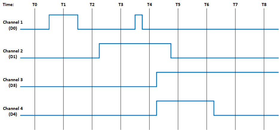
Figure 16. Example of Module's Channel-Mapped Dynamic and Latched Status States
| No Clearing of Latched Status | Clearing of Latched Status (Edge-Triggered) | Clearing of Latched Status (Level-Triggered) | ||||
| Time | Dynamic Status | Latched Status | Action | Latched Status | Action | Latched |
| T0 | 0x0 | 0x0 | Read Latched Register | 0x0 | Read Latched Register | 0x0 |
| T1 | 0x1 | 0x1 | Read Latched Register | 0x1 | 0x1 | |
| Write 0x1 to Latched Register | Write 0x1 to Latched Register | |||||
| 0x0 | 0x1 | |||||
| T2 | 0x0 | 0x1 | Read Latched Register | 0x0 | Read Latched Register | 0x1 |
| Write 0x1 to Latched Register | ||||||
| 0x0 | ||||||
| T3 | 0x2 | 0x3 | Read Latched Register | 0x2 | Read Latched Register | 0x2 |
| Write 0x2 to Latched Register | Write 0x2 to Latched Register | |||||
| 0x0 | 0x2 | |||||
| T4 | 0x2 | 0x3 | Read Latched Register | 0x1 | Read Latched Register | 0x3 |
| Write 0x1 to Latched Register | Write 0x3 to Latched Register | |||||
| 0x0 | 0x2 | |||||
| T5 | 0xC | 0xF | Read Latched Register | 0xC | Read Latched Register | 0xE |
| Write 0xC to Latched Register | Write 0xE to Latched Register | |||||
| 0x0 | 0xC | |||||
| T6 | 0xC | 0xF | Read Latched Register | 0x0 | Read Latched | 0xC |
| Write 0xC to Latched Register | ||||||
| 0xC | ||||||
| T7 | 0x4 | 0xF | Read Latched Register | 0x0 | Read Latched Register | 0xC |
| Write 0xC to Latched Register | ||||||
| 0x4 | ||||||
| T8 | 0x4 | 0xF | Read Latched Register | 0x0 | Read Latched Register | 0x4 |
Interrupt Examples
The examples in this section illustrate the interrupt behavior with Edge/Level Trigger.
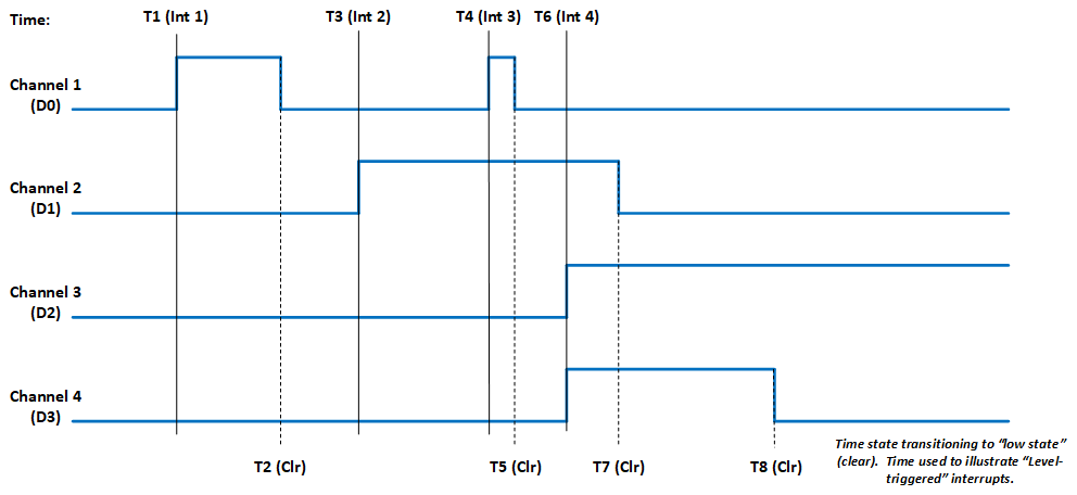
Figure 17. Illustration of Latched Status State for Module with 4-Channels with Interrupt Enabled
| Time | Latched Status (Edge-Triggered – Clear Multi-Channel) | Latched Status (Edge-Triggered – Clear Single Channel) | Latched Status (Level-Triggered – Clear Multi-Channel) | |||
| Action | Latched | Action | Latched | Action | Latched | |
| T1 (Int 1) | Interrupt Generated Read Latched Registers | 0x1 | Interrupt Generated Read Latched Registers | 0x1 | Interrupt Generated Read Latched Registers | 0x1 |
| Write 0x1 to Latched Register | Write 0x1 to Latched Register | Write 0x1 to Latched Register | ||||
| 0x0 | 0x0 | Interrupt re-triggers Note, interrupt re-triggers after each clear until T2. | 0x1 | |||
| T3 (Int 2) | Interrupt Generated Read Latched Registers | 0x2 | Interrupt Generated Read Latched Registers | 0x2 | Interrupt Generated Read Latched Registers | 0x2 |
| Write 0x2 to Latched Register | Write 0x2 to Latched Register | Write 0x2 to Latched Register | ||||
| 0x0 | 0x0 | Interrupt re-triggers Note, interrupt re-triggers after each clear until T7. | 0x2 | |||
| T4 (Int 3) | Interrupt Generated Read Latched Registers | 0x1 | Interrupt Generated Read Latched Registers | 0x1 | Interrupt Generated Read Latched Registers | 0x3 |
| Write 0x1 to Latched Register | Write 0x1 to Latched Register | Write 0x3 to Latched Register | ||||
| 0x0 | 0x0 | Interrupt re-triggers Note, interrupt re-triggers after each clear and 0x3 is reported in Latched Register until T5. | 0x3 | |||
| Interrupt re-triggers Note, interrupt re-triggers after each clear until T7. | 0x2 | |||||
| T6 (Int 4) | Interrupt Generated Read Latched Registers | 0xC | Interrupt Generated Read Latched Registers | 0xC | Interrupt Generated Read Latched Registers | 0xE |
| Write 0xC to Latched Register | Write 0x4 to Latched Register | Write 0xE to Latched Register | ||||
| 0x0 | Interrupt re-triggers Write 0x8 to Latched Register | 0x8 | Interrupt re-triggers Note, interrupt re-triggers after each clear and 0xE is reported in Latched Register until T7. | 0xE | ||
| 0x0 | Interrupt re-triggers Note, interrupt re-triggers after each clear and 0xC is reported in Latched Register until T8. | 0xC | ||||
| Interrupt re-triggers Note, interrupt re-triggers after each clear and 0x4 is reported in Latched Register always. | 0x4 | |||||
APPENDIX C: ONBOARD DISCRETE I/O USER WATCHDOG TIMER FUNCTIONALITY
Principle of Operation
The User Watchdog Timer is optionally activated by the applications that require the module’s outputs to be disabled as a failsafe in the event of an application failure or crash. The circuit is designed such that a specific periodic write strobe pattern must be executed by the software to maintain operation and prevent the disablement from taking place.
The User Watchdog Timer is inactive until the application sends an initial strobe by writing the value 0x55AA to the UWDT Strobe register. After activating the User Watchdog Timer, the application must continually strobe the timer within the intervals specified with the configurable UWDT Quiet Time and UWDT Window registers. The timing of the strobes must be consistent with the following rules:
- The application must not strobe during the Quiet time.
- The application must strobe within the Window time.
- The application must not strobe more than once in a single window time.
A violation of any of these rules will trigger a User Watchdog Timer fault and result in shutting down any isolated power supplies and/or disabling any active drive outputs, as applicable for the specific module. Upon a User Watchdog Timer event, recovery to the module shutting down will require the module to be reset.
Figures 18 and 19 provide an overview and an example with actual values for the User Watchdog Timer Strobes, Quiet Time and Window. As depicted in the diagrams, there are two processes that run in parallel. The Strobe event starts the timer for the beginning of the “Quiet Time”. The timer for the Previous Strobe event continues to run to ensure that no additional Strobes are received within the “Window” associated with the Previous Strobe.
The optimal target for the user watchdog strobes should be at the interval of [Quiet time + ½ Window time] after the previous strobe, which will place the strobe in the center of the window. This affords the greatest margin of safety against unintended disablement in critical operations.
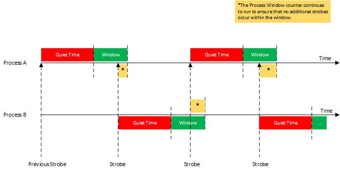
Figure 18. User Watchdog Timer Overview
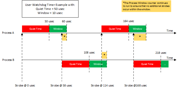
Figure 19. User Watchdog Timer Example
Figure 20 illustrates examples of User Watchdog Timer failures.
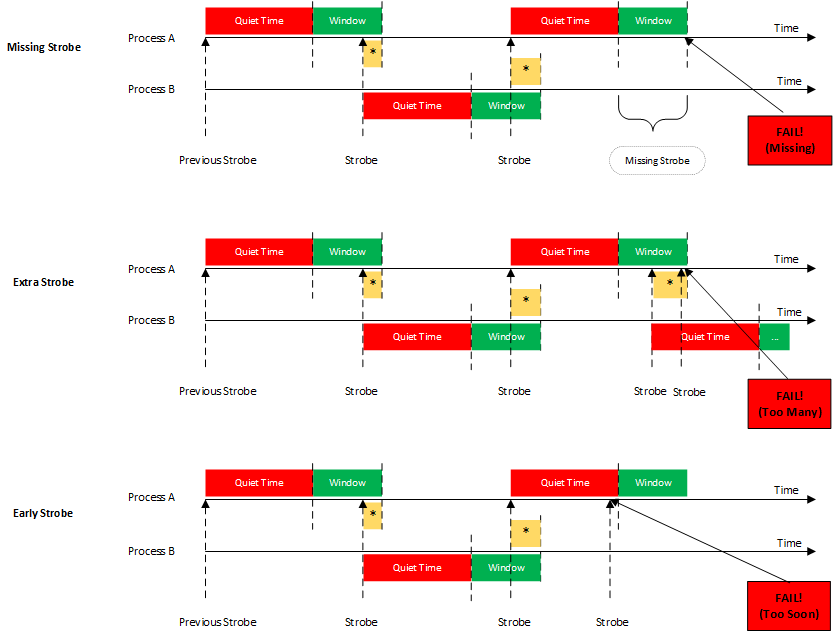
Figure 20. User Watchdog Timer Failures
Register Descriptions
The register descriptions provide the register name, Type, Data Range, Read or Write information, Initialized Value, and a description of the function.
User Watchdog Timer Registers
The registers associated with the User Watchdog Timer provide the ability to specify the UWDT Quiet Time and the UWDT Window that will be monitored to ensure that EXACTLY ONE User Watchdog Timer (UWDT) Strobe is written within the window.
| UWDT Quiet Time | |
| Function: | Sets Quiet Time value (in microseconds) to use for the User Watchdog Timer Frame. |
| Type: | unsigned binary word (32-bit) |
| Data Range: | 0 µsec to 2^32 µsec (0x0 to 0xFFFFFFFF) |
| Read/Write: | R/W |
| Initialized Value: | 0x0 |
| Operational Settings: | LSB = 1 µsec. The application must NOT write a strobe in the time between the previous strobe and the end of the Quiet time interval. In addition, the application must write in the UWDT Window EXACTLY ONCE. |
| UWDT Window | |
| Function: | Sets Window value (in microseconds) to use for the User Watchdog Timer Frame. |
| Type: | unsigned binary word (32-bit) |
| Data Range: | 0 µsec to 2^32 µsec (0x0 to 0xFFFFFFFF) |
| Read/Write: | R/W |
| Initialized Value: | 0x0 |
| Operational Settings: | LSB = 1 µsec. The application must write the strobe once within the Window time after the end of the Quiet time interval. The application must write in the UWDT Window EXACTLY ONCE. This setting must be initialized to a non-zero value for operation and should allow sufficient tolerance for strobe timing by the application. |
| UWDT Strobe | |
| Function: | Writes the strobe value to be use for the User Watchdog Timer Frame. |
| Type: | unsigned binary word (32-bit) |
| Data Range: | 0x55AA |
| Read/Write: | W |
| Initialized Value: | 0x0 |
| Operational Settings: | At startup, the user watchdog is disabled. Write the value of 0x55AA to this register to start the user watchdog timer monitoring after initial power on or a reset. To prevent a disablement, the application must periodically write the strobe based on the user watchdog timer rules. |
Status and Interrupt
The modules that are capable of User Watchdog Timer support provide status registers for the User Watchdog Timer.
User Watchdog Timer Status
The status register that contains the User Watchdog Timer Fault information is also used to indicate channel Inter-FPGA failures on modules that have communication between FPGA components. There are four registers associated with the User Watchdog Timer Fault/Inter-FPGA Failure Status: Dynamic, Latched, Interrupt Enable, and Set Edge/Level Interrupt.
| UWDT Status | |
| Function: | Sets the corresponding bit (D31) associated with the channel's User Watchdog Timer Fault error. |
| Type: | unsigned binary word (32-bit) |
| Data Range: | 0x0000 0000 to 0xFFFF FFFF |
| Read/Write: | R (Dynamic), R/W (Latched, Interrupt Enable, Set Edge/Level Interrupt) |
| Initialized Value: | 0 |
| User Watchdog Timer Fault/Inter-FPGA Failure Dynamic Status | ||
| User Watchdog Timer Fault/Inter-FPGA Failure Latched Status | ||
| User Watchdog Timer Fault/Inter-FPGA Failure Interrupt Enable | ||
| User Watchdog Timer Fault/Inter-FPGA Failure Set Edge/Level Interrupt | ||
| Bit(s) | Status | Description |
| D31 | User Watchdog Timer Fault Status | 0 = No Fault 1 = User Watchdog Timer Fault |
| D30:D0 | Reserved for Inter-FPGA Failure Status | Channel bit-mapped indicating channel inter-FPGA communication failure detection. |
Function Register Map
KEY
| Configuration/Control |
| Measurement/Status |
| USER WATCHDOG TIMER REGISTERS | |||||
| OFFSET | REGISTER NAME | ACCESS | OFFSET | REGISTER NAME | ACCESS |
| 0x01C0 | UWDT Quiet Time | R/W | |||
| 0x01C4 | UWDT Window | R/W | |||
| 0x01C8 | UWDT Strobe | R/W | |||
| STATUS REGISTERS | |||||
| *When an event is detected, the bit associated with the event is set in this register and will remain set until the user clears the event bit. Clearing the bit requires writing a 1 back to the specific bit that was set when read (i.e., write-1-to-clear, writing a “1” to a bit set to “1” will set the bit to “0”). | |||||
| OFFSET | REGISTER NAME | ACCESS | OFFSET | REGISTER NAME | ACCESS |
| 0x09B0 | Dynamic Status | R | |||
| 0x09B4 | Latched Status* | R/W | |||
| 0x09B8 | Interrupt Enable | R/W | |||
| 0x09BC | Set Edge/Level Interrupt | R/W | |||
APPENDIX D: ONBOARD DISCRETE I/O ENHANCED INPUT/OUTPUT FUNCTIONALITY
The onboard Discrete I/O function provides optional enhanced input and output mode functionality. For incoming signals (inputs), the enhanced modes include Pulse, Frequency and Period measurements. For outputs, the enhanced modes include PWM (Pulse Width Modulation) and Pattern Generation.
Input Modes
All input modes may be configured with debounce capability. Debounce capability allows configurable filtering of noisy signals and transients. Each channel may be set to an individual debounce time value. When a debounce time is set to a non-zero value, the signal reading after a transition must remain at the same level for the debounce interval before it is propagated through, otherwise it is rejected.
The waveform shown in Figure 21 will be used to illustrate the behavior for each input mode.

Figure 21. Incoming Signal Example Used to Illustrate Input Modes
Pulse Measurements
There are two Pulse Measurements features available - High Time Pulse Measurements and Low Time Pulse Measurements. The Pulse Measurement data is stored in the FIFO Buffer.
High Time Pulse Measurements
In this input mode, the data in the FIFO buffer is the measurement for each rising transition to the next falling one. Timing measurements record the time interval (in 10 µs ticks) from a pair of transitions.

Figure 22. High Time Pulse Measurement Input Mode
For this example, the FIFO Word Count register will be set to 3 and the FIFO Buffer Data register will contain the following three values (counts of 10 µs):
- 1500 (0x0000 05DC)
- 2500 (0x0000 09C4)
- 1000 (0x0000 03E8)
| Time Interval | Calculations | High Time Pulse Measurements |
| 1 | 1500 counts * 10 µsec = 15000 µsec = 15.0 msec | 15.0 msec |
| 2 | 2500 counts * 10 µsec = 25000 µsec = 25.0 msec | 25.0 msec |
| 3 | 1000 counts * 10 µsec = 10000 µsec = 10.0 msec | 10.0 msec |
Low Time Pulse Measurements
In this mode, the data in the FIFO buffer is the measurement for each falling edge to the next rising edge. Timing measurements record the time interval (in 10 µs ticks) from a pair of transitions.

Figure 23. Low Time Pulse Measurement Input Mode
For this example, the FIFO Word Count register will be set to 3 and the FIFO Buffer Data register will contain the following three values (counts of 10 µs):
- 2000 (0x0000 07D0)
- 500 (0x0000 01F4)
- 1500 (0x0000 05DC)
| Time Interval | Calculations | Low Time Pulse Measurements |
| 1 | 2000 counts * 10 µsec = 2000 µsec = 20.0 msec | 20.0 msec |
| 2 | 500 counts * 10 µsec = 5000 µsec = 5.0 msec | 5.0 msec |
| 3 | 1500 counts * 10 µsec = 15000 µsec = 15.0 msec | 15.0 msec |
Transition Timestamps
There are three Transition Timestamp Measurements features available - Transition Timestamp for All Rising Edges, Transition Timestamp for All Falling Edges, and Transition Timestamp for All Edges. The Transition Timestamps Measurement data are store in the FIFO Buffer.
Transition Timestamps of All Rising Edges
In this mode, the data in the FIFO buffer is the Rising Edge Timestamp. The timestamp is a 32-bit counter that is incremented at the rate of 100 kHz (in other words, counter is incremented every 10 µsec). The timestamp is can be reset by the application at any time.

Figure 24. Transition Timestamp of All Rising Edges Input Mode
For this example, the FIFO Word Count register will be set to 4 and the FIFO Buffer Data register will contain the following four values (counts of 10 µs):
- 1000 (0x0000 03E8)
- 4500 (0x0000 1194)
- 7500 (0x0000 1D4C)
- 10000 (0x000 2710)
This data can be interpreted as follows:
| Time Interval | Calculations | Time Between Rising Edges |
| 1 to 2 | 4500 - 1000 = 3500 counts = 3500 * 10 µsec = 35000 µsec = 35.0 msec | 35.0 msec |
| 2 to 3 | 7500 - 4500 = 3000 counts = 3000 * 10 µsec = 30000 µsec = 30.0 msec | 30.0 msec |
| 3 to 4 | 10000 - 7500 = 2500 counts = 2500 * 10 µsec = 25000 µsec = 25.0 msec | 25.0 msec |
Transition Timestamps of All Falling Edges
In this mode, the data in the FIFO buffer is the Falling Edge Timestamp. The timestamp is a 32-bit counter that is incremented at the rate of 100 kHz (in other words, counter is incremented every 10 µsec). The timestamp is can be reset by the application at any time.

Figure 25. Transition Timestamp of All Falling Edges Input Mode
For this example, the FIFO Word Count register will be set to 3 and the FIFO Buffer Data register will contain the following three values (counts of 10 µs):
- 2500 (0x0000 09C4)
- 7000 (0x0000 1B58)
- 8500 (0x0000 2134)
This data can be interpreted as follows:
| Time Interval | Calculations | Time Between Falling Edges |
| 1 to 2 | 7000 - 2500 = 4500 counts = 4500 * 10 µsec = 45000 µsec = 45.0 msec | 45.0 msec |
| 2 to 3 | 8500 - 7000 = 1500 counts = 1500 * 10 µsec = 15000 µsec = 15.0 msec | 15.0 msec |
Transition Timestamps of All Edges
In this mode, the data in the FIFO buffer is the Rising and Falling Edge Timestamp. The timestamp is a 32-bit counter that is incremented at the rate of 100 kHz (in other words, counter is incremented every 10 µsec). The timestamp is can be reset by the application at any time.

Figure 26. Transition Timestamp for All Edges Input Mode
For this example, the FIFO Word Count register will be set to 7 and the FIFO Buffer Data register will contain the following seven values (counts of 10 µs):
- 1000 (0x0000 03E8)
- 2500 (0x0000 09C4)
- 4500 (0x0000 1194)
- 7000 (0x0000 1B58)
- 7500 (0x0000 1D4C)
- 8500 (0x0000 2134)
- 10000 (0x000 2710)
This data can be interpreted as follows:
| Time Interval | Calculations | Time Between Edges |
| 1 to 2 | 2500 - 1000 = 1500 counts = 1500 * 10 µsec = 15000 µsec = 15.0 msec | 15.0 msec |
| 2 to 3 | 4500 - 2500 = 2000 counts = 2000 * 10 µsec = 20000 µsec = 20.0 msec | 20.0 msec |
| 3 to 4 | 7000 - 4500 = 2500 counts = 2500 * 10 µsec = 25000 µsec = 25.0 msec | 25.0 msec |
| 4 to 5 | 7500 - 7000 = 500 counts = 500 * 10 µsec = 5000 µsec = 5.0 msec | 5.0 msec |
| 5 to 6 | 8500 - 7500 = 1000 counts = 1000 * 10 µsec = 10000 µsec = 10.0 msec | 10.0 msec |
| 6 to 7 | 10000 - 8500 = 1500 counts = 1500 * 10 µsec = 15000 µsec = 15.0 msec | 15.0 msec |
Transition Counter
There are three Transition Counter features available - Rising Edge Transition Counter, Falling Edge Transition Counter and All Edge Transition Counter.
Rising Edges Transition Counter
In this mode, the count of the number of Rising Edges is recorded. The counter is a 32-bit counter. The counter is can be reset by the application at any time.

Figure 27. Rising Edges Transition Counter Input Mode
For this example, the Transition Count register will be set to 4.
Falling Edges Transition Counter
In this mode, the count of the number of Falling Edges is recorded. The counter is a 32-bit counter. The counter is can be reset by the application at any time.

Figure 28. Falling Edges Transition Counter Input Mode
For this example, the Transition Count register will be set to 3.
All Edges Transition Counter
In this mode, the count of the number of Rising and Falling Edges is recorded. The counter is a 32-bit counter. The counter is can be reset by the application at any time.

Figure 29. All Edges Transition Counter Input Mode
For this example, the Transition Count register will be set to 7.
Period Measurement
In this input mode, the data in the FIFO buffer is the measurement for each rising edge transition to the next rising edge transition. Timing measurements record the time interval (in 10 µs ticks).

Figure 30. Period Measurement Input Mode
For this example, the FIFO Word Count register will be set to 4 and the FIFO Buffer Data register will contain the following three values (counts of 10 µs):
- 2000 (0x0000 07D0)
- 2000 (0x0000 07D0)
- 2000 (0x0000 07D0)
- 2000 (0x0000 07D0)
| Time Interval | Calculations | Period Measurements |
| 1 | 2000 counts * 10 µsec = 20000 µsec = 20.0 msec | 20.0 msec |
| 2 | 2000 counts * 10 µsec = 20000 µsec = 20.0 msec | 20.0 msec |
| 3 | 2000 counts * 10 µsec = 20000 µsec = 20.0 msec | 20.0 msec |
| 4 | 2000 counts * 10 µsec = 20000 µsec = 20.0 msec | 20.0 msec |
Frequency Measurement
In this input mode, the data in the FIFO buffer is the number of rising edge transitions for the programmable time interval programmed in the Frequency Measurement Period register.
For this example, set the Frequency Measurement Period register = 4000 (4000 * 10 µs = 40000 µs = 40 msec).
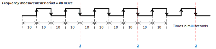
Figure 31. Frequency Measurement Input Mode
For this example, the FIFO Word Count register will be set to 3 and the FIFO Buffer Data register will contain the following three values (number of rising edges:
- 2 (0x0000 0002)
- 2 (0x0000 0002)
- 2 (0x0000 0002)
| Time Interval | Calculations | Frequency Measurements |
| 1 | 2 counts/40 msec = 2 counts/0.04 seconds = 50 Hz | 50 Hz |
| 2 | 2 counts/40 msec = 2 counts/0.04 seconds = 50 Hz | 50 Hz |
| 3 | 2 counts/40 msec = 2 counts/0.04 seconds = 50 Hz | 50 Hz |
Output Modes
There are three Enhanced Output Functionality modes: two PWM outputs and one Pattern Generator Output mode.
PWM Output
There are two PWM output modes, PWM Continuous and PWM Burst. The PWM timing is very precise with low jitter. In PWM Output mode, the Mode Select register is set to either “PWM Continuous or PWM Burst”. The value written to the PWM Period register specifies the period to output the PWM signal, the value written to the PWM Pulse Width register specifies the time for the “ON” state, and the value written to the PWM Output Polarity register specifies the initial edge of the output. For PWM Burst mode, the PWM Number of Cycles register specifies the number of cycles to output the signal. Note, there may be an initial “OFF” state level delay based on the Period time before the initial pulse is output.
PWM Continuous
Figure 32 and Figure 33 illustrate the PWM Continuous Output signal, one configured with PWM Output Polarity = Positive (0) and one configured with PWM Output Polarity = Negative (1). The configured PWM output is enabled and disabled with the Enable Measurements/Outputs register.
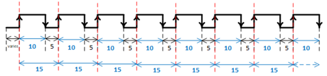
Figure 32. PWM Continuous Output
(PWM Period = 15 msec, PWM Pulse Width = 10 msec, PWM Output Polarity = Positive (0))
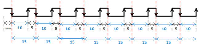
Figure 34. PWM Continuous Output
(PWM Period = 15 msec, PWM Pulse Width = 10 msec, PWM Output Polarity = Negative (1))
PWM Burst
Figure 34 and Figure 35 illustrate the PWM Burst Output signal with the PWM Number of Cycles = 5 pulses, one configured with PWM Output Polarity = Positive (0) and one configured with PWM Output Polarity = Negative (1). The configured PWM output is enabled with the Enable Measurements/Outputs register. Once the number of pulses that were requested is outputted, the value in the Enable Measurements/Outputs register will be reset (self-clearing) to allow for the output to be re-enabled.
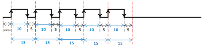
Figure 34. PWM Burst Output
(PWM Period = 15 msec, PWM Pulse Width = 10 msec, PWM Output Polarity = Positive (0),
PWM Number of Cycles = 5)
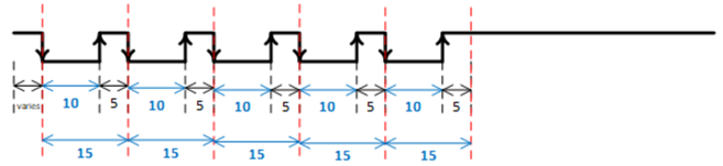
Figure 35. PWM Burst Output
(PWM Period = 15 msec, PWM Pulse Width = 10 msec, PWM Output Polarity = Negative (1)),
PWM Number of Cycles = 5)
Pattern Generator
For the Pattern Generator mode, there is 64K block of unsigned 32-bit words allocated to specify the data pattern for the output channels. The data in each 32-bit word is bit-mapped per channel. The Pattern RAM Start Address and Pattern RAM End Address registers specify the starting and ending address in the 64K block to use as the data to output for each channel configured for Pattern Generator mode. The Pattern RAM Period register specifies the pattern rate. The Pattern RAM Control and Pattern RAM Number of Cycles control the Pattern Generator output - Continuous, Burst with a specified number of cycles, Pause, or External Trigger from input from Channel 1. Note, when any channel is configured for External Trigger Pattern Generator mode, Channel 1 must be set as an input.
Figure 36 illustrates the output of the 24 channels for the Enhanced Function module all configured in Pattern Generator mode.
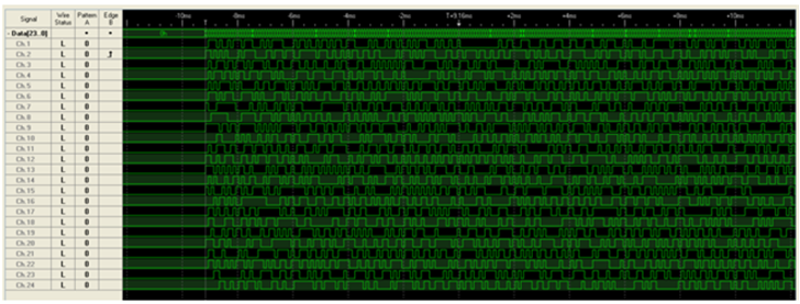
Figure 36. Pattern Generator
Enhanced Input/Output Functionality Registers
The onboard Discrete I/O option provides enhanced input and output mode functionality. The Mode Select and Enable Output/Measurement registers are general control registers for the different enhanced input and output modes.
| Mode Select | |
| Function: | Configures the Enhanced Functionality Modes to apply to the channel. |
| Type: | unsigned binary word (32-bit) |
| Data Range: | See table |
| Read/Write: | R/W |
| Initialized Value: | 0 |
| Operational Settings: | It is important that the channel is correctly configured to either input or output in the Input/Output Format registers to correspond to the Enhanced Functionality Mode selected. Setting a 0 to this register will configure that channel to normal operation. |
| Mode Select Value (Decimal) | Mode Select Value (Hexadecimal) | Description |
| 0 | 0x0000 0000 | Enhanced Functionality Disabled |
| Input Enhanced Functionality Mode | ||
| 1 | 0x0000 0001 | High Time Pulse Measurements |
| 2 | 0x0000 0002 | Low Time Pulse Measurements |
| 3 | 0x0000 0003 | Transition Timestamp of All Rising Edges |
| 4 | 0x0000 0004 | Transition Timestamp of All Falling Edges |
| 5 | 0x0000 0005 | Transition Timestamp of All Edges |
| 6 | 0x0000 0006 | Rising Edges Transition Counter |
| 7 | 0x0000 0007 | Falling Edges Transition Counter |
| 8 | 0x0000 0008 | All Edges Transition Counter |
| 9 | 0x0000 0009 | Period Measurement |
| 10 | 0x0000 000A | Frequency Measurement |
| Output Enhanced Functionality Mode | ||
| 32 | 0x0000 0020 | PWM Continuous |
| 33 | 0x0000 0021 | PWM Burst |
| 34 | 0x0000 0022 | Pattern Generator |
| Enable Measurements/Outputs | |
| Function: | Enables/starts the measurements or outputs based on the Mode Select for the channel. |
| Type: | unsigned binary word (32-bit) |
| Data Range: | 0x0000 0000 to 0x00FF FFFF |
| Read/Write: | R/W |
| Initialized Value: | 0 |
| Operational Settings: | Setting the bit for the associated channel to a 1 will start the measurement or output depending on the Mode Select configuration for that channel. Setting the bit for the associated channel to 0 will stop the measurements/outputs. |
| D31 | D30 | D29 | D28 | D27 | D26 | D25 | D24 | D23 | D22 | D21 | D20 | D19 | D18 | D17 | D16 |
| 0 | 0 | 0 | 0 | 0 | 0 | 0 | 0 | Ch24 | Ch23 | Ch22 | Ch21 | Ch20 | Ch19 | Ch18 | Ch17 |
| D15 | D14 | D13 | D12 | D11 | D10 | D9 | D8 | D7 | D6 | D5 | D4 | D3 | D2 | D1 | D0 |
| Ch16 | Ch15 | Ch14 | Ch13 | Ch12 | Ch11 | Ch10 | Ch9 | Ch8 | Ch7 | Ch6 | Ch5 | Ch4 | Ch3 | Ch2 | Ch1 |
Input Mode Registers
After configuring the Mode Select register, write a 1 to the Reset Timer/Counter register resets the channel’s timestamp and counter used for input modes. Write a 1 to the Enable Measurements/Outputs register to begin the measurement of the input signal. Write a 0 to the Enable Measurements/Outputs register to stop the measurement of the input signal. The data can be read either while the measurements are being made on input signals or after stopping the measurements.
| Reset Timer/Counter | |
| Function: | Resets the measurement timestamp and counter for the channel. |
| Type: | unsigned binary word (32-bit) |
| Data Range: | 0x0000 0000 to 0x00FF FFFF |
| Read/Write: | W |
| Initialized Value: | 0 |
| Operational Settings: | Setting the bit for the associated channel to a 1 will: * reset the timestamp used for the Pulse Measurements mode (1-2), Transition Timestamp mode (3-5), and Period Measurement mode (9) and Frequency Measurement mode (10) * reset the counter used for Transition Counter mode (6-8) |
| D31 | D30 | D29 | D28 | D27 | D26 | D25 | D24 | D23 | D22 | D21 | D20 | D19 | D18 | D17 | D16 |
| 0 | 0 | 0 | 0 | 0 | 0 | 0 | 0 | Ch24 | Ch23 | Ch22 | Ch21 | Ch20 | Ch19 | Ch18 | Ch17 |
| D15 | D14 | D13 | D12 | D11 | D10 | D9 | D8 | D7 | D6 | D5 | D4 | D3 | D2 | D1 | D0 |
| Ch16 | Ch15 | Ch14 | Ch13 | Ch12 | Ch11 | Ch10 | Ch9 | Ch8 | Ch7 | Ch6 | Ch5 | Ch4 | Ch3 | Ch2 | Ch1 |
FIFO Registers
The FIFO registers are used for the following input modes:
- Pulse Measurements mode (1-2)
- Transition Timestamp mode (3-5)
- Period Measurement mode (9)
- Frequency Measurement mode (10)
| FIFO Buffer Data | |
| Function: | The data stored in the FIFO Buffer Data is dependent on the input mode. |
| Type: | unsigned binary word (32-bit) |
| Data Range: | 0x0000 0000 to 0xFFFF FFFF |
| Read/Write: | R |
| Initialized Value: | N/A |
| Operational Settings: | Refer to examples in Input Modes. |
| FIFO Word Count | |
| Function: | This is a counter that reports the number of 32-bit words stored in the FIFO buffer. |
| Type: | unsigned binary word (32-bit) |
| Data Range: | 0 - 255 (0x0000 0000 to 0x0000 00FF) |
| Read/Write: | R |
| Initialized Value: | 0 |
| Operational Settings: | Every time a read operation is made from the FIFO Buffer Data register, the value in the FIFO Word Count register will be decremented by one. The maximum number of words that can be stored in the FIFO is 255. |
| D31 | D30 | D29 | D28 | D27 | D26 | D25 | D24 | D23 | D22 | D21 | D20 | D19 | D18 | D17 | D16 |
| 0 | 0 | 0 | 0 | 0 | 0 | 0 | 0 | 0 | 0 | 0 | 0 | 0 | 0 | 0 | 0 |
| D15 | D14 | D13 | D12 | D11 | D10 | D9 | D8 | D7 | D6 | D5 | D4 | D3 | D2 | D1 | D0 |
| 0 | 0 | 0 | 0 | 0 | 0 | 0 | D | D | D | D | D | D | D | D | D |
| Clear FIFO | |
| Function: | Clears FIFO by resetting the FIFO Word Count register. |
| Type: | unsigned binary word (32-bit) |
| Data Range: | 0 or 1 |
| Read/Write: | W |
| Initialized Value: | N/A |
| Operational Settings: | Write a 1 to resets the Words in FIFO to zero; Clear FIFO register does not clear data in the buffer. A read to the buffer data will give “aged” data. |
| Bit | Description |
| D31:D1 | Reserved. Set to 0 |
| D0 | Set to 1 to reset the FIFO Word Count value to zero. |
| D31 | D30 | D29 | D28 | D27 | D26 | D25 | D24 | D23 | D22 | D21 | D20 | D19 | D18 | D17 | D16 |
| 0 | 0 | 0 | 0 | 0 | 0 | 0 | 0 | 0 | 0 | 0 | 0 | 0 | 0 | 0 | 0 |
| D15 | D14 | D13 | D12 | D11 | D10 | D9 | D8 | D7 | D6 | D5 | D4 | D3 | D2 | D1 | D0 |
| 0 | 0 | 0 | 0 | 0 | 0 | 0 | 0 | 0 | 0 | 0 | 0 | 0 | 0 | 0 | D |
| FIFO Status | |
| Function: | Sets the corresponding bit associated with the FIFO status type; there is a separate register for each channel. |
| Type: | unsigned binary word (32-bit) |
| Data Range: | See table |
| Read/Write: | R |
| Initialized Value: | 0 |
| Bit | Name | Description |
| D31:D4 | Reserved | Set to 0 |
| D3 | Empty | Set to 1 when FIFO Word Count = 0 |
| D2 | Almost Empty | Set to 1 when FIFO Word Count <= 63 (25%) |
| D1 | Almost Full | Set to 1 when FIFO Word Count >= 191 (75%) |
| D0 | Full | Set to 1 when FIFO Word Count = 255 |
| D31 | D30 | D29 | D28 | D27 | D26 | D25 | D24 | D23 | D22 | D21 | D20 | D19 | D18 | D17 | D16 |
| 0 | 0 | 0 | 0 | 0 | 0 | 0 | 0 | 0 | 0 | 0 | 0 | 0 | 0 | 0 | 0 |
| D15 | D14 | D13 | D12 | D11 | D10 | D9 | D8 | D7 | D6 | D5 | D4 | D3 | D2 | D1 | D0 |
| 0 | 0 | 0 | 0 | 0 | 0 | 0 | 0 | 0 | 0 | 0 | 0 | D | D | D | D |
Transition Count Registers
The Transition Count register are used for the following input modes:
Transition Counter mode (6-8)
| Transition Count | |
| Function: | Contains the count of the transitions depending on the configuration in the Mode Select register - Rising Edges, Falling Edges or All Edges. |
| Type: | unsigned binary word (32-bit) |
| Data Range: | 0x0000 0000 to 0xFFFF FFFF |
| Read/Write: | R |
| Initialized Value: | 0 |
| Operational Settings: | Refer to examples in Transition Counter. |
Frequency Measurement Registers
For the Frequency Measurement mode, the period to perform the frequency measurements must be specified in the Frequency Measurement Period register.
| Frequency Measurement Period | |
| Function: | When the Mode Select register is programmed for Frequency Measurement mode (10), the value in the Frequency Measurement Period is used as the time interval for counting the number of rising edge transitions within that interval. |
| Type: | unsigned binary word (32-bit) |
| Data Range: | 0x0 to 0xFFFF FFFF |
| Read/Write: | R/W |
| Initialized Value: | 0 |
| Operational Settings: | Set the Frequency Measurement Period (LSB = 10 µs). Refer to examples in Frequency Measurement. |
Output Modes Registers
After configuring the Mode Select register, write a 1 to the Enable Measurements/Outputs register to outputting the signal. Write a 0 to the Enable Measurements/Outputs register to stop the output signal.
PWM Registers
The PWM Period, PWM Pulse Width and PWM Output Polarity registers configure the PWM output signal. When the Mode Select register is configured for PWM Burst mode, the PWM Number of Cycles register is used to specify the number of cycles to repeat for the burst.
| PWM Period | |
| Function: | When the Mode Select register is programmed for PWM Continuous or PWM Burst mode (32-33), the value in the PWM Period is used as the time interval for outputting the PWM signal. |
| Type: | unsigned binary word (32-bit) |
| Data Range: | 0x0000 0001 to 0xFFFF FFFF |
| Read/Write: | R/W |
| Initialized Value: | 0 |
| Operational Settings: | Set the PWM Period (LSB = 10 µs). The PWM Period must be greater than the value set in the PWM Pulse Width register. Refer to examples in PWM Output. |
| PWM Pulse Width | |
| Function: | When the Mode Select register is programmed for PWM Continuous or PWM Burst mode (32-33), the value in the PWM Pulse Width is used as the time interval of the “ON” state for outputting the PWM signal. |
| Type: | unsigned binary word (32-bit) |
| Data Range: | 0x0 to 0xFFFF FFFF |
| Read/Write: | R/W |
| Initialized Value: | 0 |
| Operational Settings: | Set the PWM Pulse Width (LSB = 10 µs). The PWM Pulse Width must be less than the value set in the PWM Pulse Width register. Refer to examples in PWM Output. |
| PWM Output Polarity | |
| Function: | When the Mode Select register is programmed for PWM Continuous or PWM Burst mode (32-33), the value in the PWM Output Polarity is used to specify whether the PWM output signal starts with a rising edge (Positive (0)), or a falling edge (Negative (1)). |
| Type: | unsigned binary word (32-bit) |
| Data Range: | 0x0 to 0x00FF FFFF |
| Read/Write: | R/W |
| Initialized Value: | 0 |
| Operational Settings: | The PWM Output Polarity register is used to program the starting edge of the PWM Pulse Period (rising or falling). When the PWM output Polarity is set to Positive (0), the output will start with a rising edge, when it's set to Negative (1), the output will start with a falling edge. The default is Positive (0), which is set when the PWM Polarity bit is 0. Refer to examples in PWM Output. |
| D31 | D30 | D29 | D28 | D27 | D26 | D25 | D24 | D23 | D22 | D21 | D20 | D19 | D18 | D17 | D16 |
| 0 | 0 | 0 | 0 | 0 | 0 | 0 | 0 | Ch24 | Ch23 | Ch22 | Ch21 | Ch20 | Ch19 | Ch18 | Ch17 |
| D15 | D14 | D13 | D12 | D11 | D10 | D9 | D8 | D7 | D6 | D5 | D4 | D3 | D2 | D1 | D0 |
| Ch16 | Ch15 | Ch14 | Ch13 | Ch12 | Ch11 | Ch10 | Ch9 | Ch8 | Ch7 | Ch6 | Ch5 | Ch4 | Ch3 | Ch2 | Ch1 |
| PWM Number of Cycles | |
| Function: | When the Mode Select register is programmed for PWM Burst mode (33), the value in the PWM Number of Cycles is used to specify the number of times to repeat the PWM output signal. |
| Type: | unsigned binary word (32-bit) |
| Data Range: | 0x0000 0001 to 0xFFFF FFFF |
| Read/Write: | R/W |
| Initialized Value: | 0 |
| Operational Settings: | Set the number of times to output the PWM signal. Refer to examples in PWM Output. |
Pattern Generator Registers
The Pattern RAM registers are a 64K block of unsigned 32-bit words allocated to specify the data pattern for the output channels. The Pattern RAM Start Address, Pattern RAM End Address, Pattern RAM Period and Pattern RAM Control registers configure the Pattern Generator output signals. When the Pattern RAM Control register is configured for Burst, the Pattern RAM Number of Cycles specify the number of cycles to repeat the pattern for the burst.
| Pattern RAM | |
| Function: | Pattern Generator Memory Block from 0x40000 to 0x7FFFC. |
| Type: | unsigned binary word (32-bit) |
| Address Range: | 0x0000 0000 to 0x00FF FFFF |
| Read/Write: | R/W |
| Initialized Value: | 0 |
| Operational Settings: | 64K block of unsigned 32-bit words. The data in each 32-bit word is bit-mapped per channel. |
| D31 | D30 | D29 | D28 | D27 | D26 | D25 | D24 | D23 | D22 | D21 | D20 | D19 | D18 | D17 | D16 |
| 0 | 0 | 0 | 0 | 0 | 0 | 0 | 0 | Ch24 | Ch23 | Ch22 | Ch21 | Ch20 | Ch19 | Ch18 | Ch17 |
| D15 | D14 | D13 | D12 | D11 | D10 | D9 | D8 | D7 | D6 | D5 | D4 | D3 | D2 | D1 | D0 |
| Ch16 | Ch15 | Ch14 | Ch13 | Ch12 | Ch11 | Ch10 | Ch9 | Ch8 | Ch7 | Ch6 | Ch5 | Ch4 | Ch3 | Ch2 | Ch1 |
| Pattern RAM Start Address | |
| Function: | When the Mode Select register is programmed for Pattern Generator mode (34), the Pattern RAM Start Address register specifies the starting address within the Pattern RAM block registers to use for the output. |
| Type: | unsigned binary word (32-bit) |
| Data Range: | 0x0004 0000 to 0x0007 FFFC |
| Read/Write: | R/W |
| Initialized Value: | 0 |
| Operational Settings: | The value in the Pattern RAM Start Address must be LESS than the value in the Pattern RAM End Address. |
| D31 | D30 | D29 | D28 | D27 | D26 | D25 | D24 | D23 | D22 | D21 | D20 | D19 | D18 | D17 | D16 |
| 0 | 0 | 0 | 0 | 0 | 0 | 0 | 0 | 0 | 0 | 0 | 0 | 0 | D | D | D |
| D15 | D14 | D13 | D12 | D11 | D10 | D9 | D8 | D7 | D6 | D5 | D4 | D3 | D2 | D1 | D0 |
| D | D | D | D | D | D | D | D | D | D | D | D | D | D | D | D |
| Pattern RAM End Address | |
| Function: | When the Mode Select register is programmed for Pattern Generator mode (34), the Pattern RAM End Address register specifies the end address within the Pattern RAM block registers to use for the output. |
| Type: | unsigned binary word (32-bit) |
| Data Range: | 0x40000 to 0x7FFFC |
| Read/Write: | R/W |
| Initialized Value: | 0 |
| Operational Settings: | The value in the Pattern RAM End Address must be GREATER than the value in the Pattern RAM Start Address. |
| D31 | D30 | D29 | D28 | D27 | D26 | D25 | D24 | D23 | D22 | D21 | D20 | D19 | D18 | D17 | D16 |
| 0 | 0 | 0 | 0 | 0 | 0 | 0 | 0 | 0 | 0 | 0 | 0 | 0 | D | D | D |
| D15 | D14 | D13 | D12 | D11 | D10 | D9 | D8 | D7 | D6 | D5 | D4 | D3 | D2 | D1 | D0 |
| D | D | D | D | D | D | D | D | D | D | D | D | D | D | D | D |
| Pattern RAM Period | |
| Function: | When the Mode Select register is programmed for Pattern Generator mode (34), the value in the Pattern RAM Period is used as the time interval for outputting the Pattern Generator signals. |
| Type: | unsigned binary word (32-bit) |
| Data Range: | 0x0000 0001 to 0xFFFF FFFF |
| Read/Write: | R/W |
| Initialized Value: | 0 |
| Operational Settings: | Set the Pattern RAM Period (LSB = 10 µs). |
| Pattern RAM Control | |
| Function: | When the Mode Select register is programmed for Pattern Generator mode (34), the value in the Pattern RAM Control is used to control the outputting of the Pattern Generator signals. |
| Type: | unsigned binary word (32-bit) |
| Data Range: | See table |
| Read/Write: | R/W |
| Initialized Value: | 0 |
| Operational Settings: | Configures the Pattern Generator for Continuous, Burst with a specified number of cycles, Pause, or External Trigger from input from Channel 1. |
Note
When any channel is configured for External Trigger Pattern Generator mode, Channel 1 MUST be set as an input.
| Bits | Description |
| D31-D5 | Reserved. Set to 0 |
| D4 | Falling Edge External Trigger - Channel 1 used as the input for the trigger |
| D3 | Rising Edge External Trigger - Channel 1 used as the input for the trigger |
| D2 | Pause |
| D1 | Burst Mode - value in Pattern RAM Number of Cycles register defines number of cycles to output |
| D0 | Enable Pattern Generator |
| Values | Description |
| 0x0000 | Disable Pattern Generator, Continuous Mode, No External Trigger |
| 0x0001 | Enable Pattern Generator, Continuous Mode, No External Trigger |
| 0x0002 | Disable Pattern Generator, Burst Mode, No External Trigger |
| 0x0003 | Enable Pattern Generator, Burst Mode, No External Trigger |
| 0x0005 | Enable Pattern Generator, Continuous Mode, Pause, No External Trigger |
| 0x0007 | Enable Pattern Generator, Burst Mode, Pause, No External Trigger |
| 0x0008 | Disable Pattern Generator, Continuous Mode, Rising External Trigger |
| 0x0009 | Enable Pattern Generator, Continuous Mode, Rising External Trigger |
| 0x000A | Disable Pattern Generator, Burst Mode, Rising External Trigger |
| 0x000B | Enable Pattern Generator, Burst Mode, Rising External Trigger |
| 0x000D | Enable Pattern Generator, Continuous Mode, Pause, Rising External Trigger |
| 0x000F | Enable Pattern Generator, Burst Mode, Pause, Rising External Trigger |
| 0x1000 | Disable Pattern Generator, Continuous Mode, Falling External Trigger |
| 0x1001 | Enable Pattern Generator, Continuous Mode, Falling External Trigger |
| 0x1002 | Disable Pattern Generator, Burst Mode, Falling External Trigger |
| 0x1003 | Enable Pattern Generator, Burst Mode, Falling External Trigger |
| 0x1005 | Enable Pattern Generator, Continuous Mode, Pause, Falling External Trigger |
| 0x1007 | Enable Pattern Generator, Burst Mode, Pause, Falling External Trigger |
| 0x0004, 0x0006, 0x000C, 0x000E, 0x1004, 0x1006, 0x1008-0x100F | Invalid |
| D31 | D30 | D29 | D28 | D27 | D26 | D25 | D24 | D23 | D22 | D21 | D20 | D19 | D18 | D17 | D16 |
| 0 | 0 | 0 | 0 | 0 | 0 | 0 | 0 | 0 | 0 | 0 | 0 | 0 | 0 | 0 | 0 |
| D15 | D14 | D13 | D12 | D11 | D10 | D9 | D8 | D7 | D6 | D5 | D4 | D3 | D2 | D1 | D0 |
| 0 | 0 | 0 | 0 | 0 | 0 | 0 | 0 | 0 | 0 | 0 | 0 | D | D | D | D |
| Pattern RAM Number of Cycles | |
| Function: | When the Mode Select register is programmed for Pattern Generator mode (34) and the Pattern RAM Control register is set for Burst mode, the value in the Pattern RAM Number of Cycles is used to specify the number of times to repeat the pattern output signal. |
| Type: | unsigned binary word (32-bit) |
| Data Range: | 0x0000 0001 to 0xFFFF FFFF |
| Read/Write: | R/W |
| Initialized Value: | 0 |
| Operational Settings: | Set the number of times to output the pattern. |
Function Register Map
Key:
| Configuration/Control |
| Status |
| MODE SELECT REGISTERS | |||||
| OFFSET | REGISTER NAME | ACCESS | OFFSET | REGISTER NAME | ACCESS |
| 0x300C | Mode Select Ch 1 | R/W | |||
| 0x308C | Mode Select Ch 2 | R/W | |||
| 0x310C | Mode Select Ch 3 | R/W | |||
| 0x318C | Mode Select Ch 4 | R/W | |||
| 0x320C | Mode Select Ch 5 | R/W | |||
| 0x328C | Mode Select Ch 6 | R/W | |||
| 0x330C | Mode Select Ch 7 | R/W | |||
| 0x338C | Mode Select Ch 8 | R/W | |||
| 0x340C | Mode Select Ch 9 | R/W | |||
| 0x348C | Mode Select Ch 10 | R/W | |||
| 0x350C | Mode Select Ch 11 | R/W | |||
| 0x358C | Mode Select Ch 12 | R/W | |||
| 0x360C | Mode Select Ch 13 | R/W | |||
| 0x368C | Mode Select Ch 14 | R/W | |||
| 0x370C | Mode Select Ch 15 | R/W | |||
| 0x378C | Mode Select Ch 16 | R/W | |||
| 0x380C | Mode Select Ch 17 | R/W | |||
| 0x388C | Mode Select Ch 18 | R/W | |||
| 0x390C | Mode Select Ch 19 | R/W | |||
| 0x398C | Mode Select Ch 20 | R/W | |||
| 0x3A0C | Mode Select Ch 21 | R/W | |||
| 0x3A8C | Mode Select Ch 22 | R/W | |||
| 0x3B0C | Mode Select Ch 23 | R/W | |||
| 0x3B8C | Mode Select Ch 24 | R/W | |||
| 0x2000 | Enable Measurements/Outputs | R/W | |||
| INPUT MODES REGISTER | |||||
| OFFSET | REGISTER NAME | ACCESS | OFFSET | REGISTER NAME | ACCESS |
| 0x2004 | Reset Timer/Counter | W | |||
| FIFO REGISTERS | |||||
| OFFSET | REGISTER NAME | ACCESS | OFFSET | REGISTER NAME | ACCESS |
| 0x3000 | FIFO Buffer Data Ch 1 | R | 0x3004 | FIFO Word Count Ch 1 | R |
| 0x3080 | FIFO Buffer Data Ch 2 | R | 0x3084 | FIFO Word Count Ch 2 | R |
| 0x3100 | FIFO Buffer Data Ch 3 | R | 0x3104 | FIFO Word Count Ch 3 | R |
| 0x3180 | FIFO Buffer Data Ch 4 | R | 0x3184 | FIFO Word Count Ch 4 | R |
| 0x3200 | FIFO Buffer Data Ch 5 | R | 0x3204 | FIFO Word Count Ch 5 | R |
| 0x3280 | FIFO Buffer Data Ch 6 | R | 0x3284 | FIFO Word Count Ch 6 | R |
| 0x3300 | FIFO Buffer Data Ch 7 | R | 0x3304 | FIFO Word Count Ch 7 | R |
| 0x3380 | FIFO Buffer Data Ch 8 | R | 0x3384 | FIFO Word Count Ch 8 | R |
| 0x3400 | FIFO Buffer Data Ch 9 | R | 0x3404 | FIFO Word Count Ch 9 | R |
| 0x3480 | FIFO Buffer Data Ch 10 | R | 0x3484 | FIFO Word Count Ch 10 | R |
| 0x3500 | FIFO Buffer Data Ch 11 | R | 0x3504 | FIFO Word Count Ch 11 | R |
| 0x3580 | FIFO Buffer Data Ch 12 | R | 0x3584 | FIFO Word Count Ch 12 | R |
| 0x3600 | FIFO Buffer Data Ch 13 | R | 0x3604 | FIFO Word Count Ch 13 | R |
| 0x3680 | FIFO Buffer Data Ch 14 | R | 0x3684 | FIFO Word Count Ch 14 | R |
| 0x3700 | FIFO Buffer Data Ch 15 | R | 0x3704 | FIFO Word Count Ch 15 | R |
| 0x3780 | FIFO Buffer Data Ch 16 | R | 0x3784 | FIFO Word Count Ch 16 | R |
| 0x3800 | FIFO Buffer Data Ch 17 | R | 0x3804 | FIFO Word Count Ch 17 | R |
| 0x3880 | FIFO Buffer Data Ch 18 | R | 0x3884 | FIFO Word Count Ch 18 | R |
| 0x3900 | FIFO Buffer Data Ch 19 | R | 0x3904 | FIFO Word Count Ch 19 | R |
| 0x3980 | FIFO Buffer Data Ch 20 | R | 0x3984 | FIFO Word Count Ch 20 | R |
| 0x3A00 | FIFO Buffer Data Ch 21 | R | 0x3A04 | FIFO Word Count Ch 21 | R |
| 0x3A80 | FIFO Buffer Data Ch 22 | R | 0x3A84 | FIFO Word Count Ch 22 | R |
| 0x3B00 | FIFO Buffer Data Ch 23 | R | 0x3B04 | FIFO Word Count Ch 23 | R |
| 0x3B80 | FIFO Buffer Data Ch 24 | R | 0x3B84 | FIFO Word Count Ch 24 | R |
| 0x3008 | FIFO Status Ch 1 | R | |||
| 0x3088 | FIFO Status Ch 2 | R | |||
| 0x3108 | FIFO Status Ch 3 | R | |||
| 0x3188 | FIFO Status Ch 4 | R | |||
| 0x3208 | FIFO Status Ch 5 | R | |||
| 0x3288 | FIFO Status Ch 6 | R | |||
| 0x3308 | FIFO Status Ch 7 | R | |||
| 0x3388 | FIFO Status Ch 8 | R | |||
| 0x3408 | FIFO Status Ch 9 | R | |||
| 0x3488 | FIFO Status Ch 10 | R | |||
| 0x3508 | FIFO Status Ch 11 | R | |||
| 0x3588 | FIFO Status Ch 12 | R | |||
| 0x3608 | FIFO Status Ch 13 | R | |||
| 0x3688 | FIFO Status Ch 14 | R | |||
| 0x3708 | FIFO Status Ch 15 | R | |||
| 0x3788 | FIFO Status Ch 16 | R | |||
| 0x3808 | FIFO Status Ch 17 | R | |||
| 0x3888 | FIFO Status Ch 18 | R | |||
| 0x3908 | FIFO Status Ch 19 | R | |||
| 0x3988 | FIFO Status Ch 20 | R | |||
| 0x3A08 | FIFO Status Ch 21 | R | |||
| 0x3A88 | FIFO Status Ch 22 | R | |||
| 0x3B08 | FIFO Status Ch 23 | R | |||
| 0x3B88 | FIFO Status Ch 24 | R | |||
| 0x2008 | Reset FIFO | W | |||
| TRANSITION COUNT REGISTERS | |||||
| OFFSET | REGISTER NAME | ACCESS | OFFSET | REGISTER NAME | ACCESS |
| 0x3000 | Transition Count Ch 1 | R | |||
| 0x3080 | Transition Count Ch 2 | R | |||
| 0x3100 | Transition Count Ch 3 | R | |||
| 0x3180 | Transition Count Ch 4 | R | |||
| 0x3200 | Transition Count Ch 5 | R | |||
| 0x3280 | Transition Count Ch 6 | R | |||
| 0x3300 | Transition Count Ch 7 | R | |||
| 0x3380 | Transition Count Ch 8 | R | |||
| 0x3400 | Transition Count Ch 9 | R | |||
| 0x3480 | Transition Count Ch 10 | R | |||
| 0x3500 | Transition Count Ch 11 | R | |||
| 0x3580 | Transition Count Ch 12 | R | |||
| 0x3600 | Transition Count Ch 13 | R | |||
| 0x3680 | Transition Count Ch 14 | R | |||
| 0x3700 | Transition Count Ch 15 | R | |||
| 0x3780 | Transition Count Ch 16 | R | |||
| 0x3800 | Transition Count Ch 17 | R | |||
| 0x3880 | Transition Count Ch 18 | R | |||
| 0x3900 | Transition Count Ch 19 | R | |||
| 0x3980 | Transition Count Ch 20 | R | |||
| 0x3A00 | Transition Count Ch 21 | R | |||
| 0x3A80 | Transition Count Ch 22 | R | |||
| 0x3B00 | Transition Count Ch 23 | R | |||
| 0x3B80 | Transition Count Ch 24 | R | |||
| FREQUENCY MEASUREMENT REGISTERS | |||||
| NOTE: Base Address - 0x9010 C000 | |||||
| OFFSET | REGISTER NAME | ACCESS | OFFSET | REGISTER NAME | ACCESS |
| 0x3014 | Frequency Measurement Period Ch 1 | R/W | |||
| 0x3094 | Frequency Measurement Period Ch 2 | R/W | |||
| 0x3114 | Frequency Measurement Period Ch 3 | R/W | |||
| 0x3194 | Frequency Measurement Period Ch 4 | R/W | |||
| 0x3214 | Frequency Measurement Period Ch 5 | R/W | |||
| 0x3294 | Frequency Measurement Period Ch 6 | R/W | |||
| 0x3314 | Frequency Measurement Period Ch 7 | R/W | |||
| 0x3394 | Frequency Measurement Period Ch 8 | R/W | |||
| 0x3414 | Frequency Measurement Period Ch 9 | R/W | |||
| 0x3494 | Frequency Measurement Period Ch 10 | R/W | |||
| 0x3514 | Frequency Measurement Period Ch 11 | R/W | |||
| 0x3594 | Frequency Measurement Period Ch 12 | R/W | |||
| 0x3614 | Frequency Measurement Period Ch 13 | R/W | |||
| 0x3694 | Frequency Measurement Period Ch 14 | R/W | |||
| 0x3714 | Frequency Measurement Period Ch 15 | R/W | |||
| 0x3794 | Frequency Measurement Period Ch 16 | R/W | |||
| 0x3814 | Frequency Measurement Period Ch 17 | R/W | |||
| 0x3894 | Frequency Measurement Period Ch 18 | R/W | |||
| 0x3914 | Frequency Measurement Period Ch 19 | R/W | |||
| 0x3994 | Frequency Measurement Period Ch 20 | R/W | |||
| 0x3A14 | Frequency Measurement Period Ch 21 | R/W | |||
| 0x3A94 | Frequency Measurement Period Ch 22 | R/W | |||
| 0x3B14 | Frequency Measurement Period Ch 23 | R/W | |||
| 0x3B94 | Frequency Measurement Period Ch 24 | R/W | |||
Output Mode Registers
| PWM REGISTERS | |||||
| OFFSET | REGISTER NAME | ACCESS | OFFSET | REGISTER NAME | ACCESS |
| 0x3014 | PWM Period Ch 1 | R/W | 0x3010 | PWM Pulse Width Ch 1 | R/W |
| 0x3094 | PWM Period Ch 2 | R/W | 0x3090 | PWM Pulse Width Ch 2 | R/W |
| 0x3114 | PWM Period Ch 3 | R/W | 0x3110 | PWM Pulse Width Ch 3 | R/W |
| 0x3194 | PWM Period Ch 4 | R/W | 0x3190 | PWM Pulse Width Ch 4 | R/W |
| 0x3214 | PWM Period Ch 5 | R/W | 0x3210 | PWM Pulse Width Ch 5 | R/W |
| 0x3294 | PWM Period Ch 6 | R/W | 0x3290 | PWM Pulse Width Ch 6 | R/W |
| 0x3314 | PWM Period Ch 7 | R/W | 0x3310 | PWM Pulse Width Ch 7 | R/W |
| 0x3394 | PWM Period Ch 8 | R/W | 0x3390 | PWM Pulse Width Ch 8 | R/W |
| 0x3414 | PWM Period Ch 9 | R/W | 0x3410 | PWM Pulse Width Ch 9 | R/W |
| 0x3494 | PWM Period Ch 10 | R/W | 0x3490 | PWM Pulse Width Ch 10 | R/W |
| 0x3514 | PWM Period Ch 11 | R/W | 0x3510 | PWM Pulse Width Ch 11 | R/W |
| 0x3594 | PWM Period Ch 12 | R/W | 0x3590 | PWM Pulse Width Ch 12 | R/W |
| 0x3614 | PWM Period Ch 13 | R/W | 0x3610 | PWM Pulse Width Ch 13 | R/W |
| 0x3694 | PWM Period Ch 14 | R/W | 0x3690 | PWM Pulse Width Ch 14 | R/W |
| 0x3714 | PWM Period Ch 15 | R/W | 0x3710 | PWM Pulse Width Ch 15 | R/W |
| 0x3794 | PWM Period Ch 16 | R/W | 0x3790 | PWM Pulse Width Ch 16 | R/W |
| 0x3814 | PWM Period Ch 17 | R/W | 0x3810 | PWM Pulse Width Ch 17 | R/W |
| 0x3894 | PWM Period Ch 18 | R/W | 0x3890 | PWM Pulse Width Ch 18 | R/W |
| 0x3914 | PWM Period Ch 19 | R/W | 0x3910 | PWM Pulse Width Ch 19 | R/W |
| 0x3994 | PWM Period Ch 20 | R/W | 0x3990 | PWM Pulse Width Ch 20 | R/W |
| 0x3A14 | PWM Period Ch 21 | R/W | 0x3A10 | PWM Pulse Width Ch 21 | R/W |
| 0x3A94 | PWM Period Ch 22 | R/W | 0x3A90 | PWM Pulse Width Ch 22 | R/W |
| 0x3B14 | PWM Period Ch 23 | R/W | 0x3B10 | PWM Pulse Width Ch 23 | R/W |
| 0x3B94 | PWM Period Ch 24 | R/W | 0x3B90 | PWM Pulse Width Ch 24 | R/W |
| 0x3018 | PWM Number of Cycles Ch 1 | R/W | |||
| 0x3098 | PWM Number of Cycles Ch 2 | R/W | |||
| 0x3118 | PWM Number of Cycles Ch 3 | R/W | |||
| 0x3198 | PWM Number of Cycles Ch 4 | R/W | |||
| 0x3218 | PWM Number of Cycles Ch 5 | R/W | |||
| 0x3298 | PWM Number of Cycles Ch 6 | R/W | |||
| 0x3318 | PWM Number of Cycles Ch 7 | R/W | |||
| 0x3398 | PWM Number of Cycles Ch 8 | R/W | |||
| 0x3418 | PWM Number of Cycles Ch 9 | R/W | |||
| 0x3498 | PWM Number of Cycles Ch 10 | R/W | |||
| 0x3518 | PWM Number of Cycles Ch 11 | R/W | |||
| 0x3598 | PWM Number of Cycles Ch 12 | R/W | |||
| 0x3618 | PWM Number of Cycles Ch 13 | R/W | |||
| 0x3698 | PWM Number of Cycles Ch 14 | R/W | |||
| 0x3718 | PWM Number of Cycles Ch 15 | R/W | |||
| 0x3798 | PWM Number of Cycles Ch 16 | R/W | |||
| 0x3818 | PWM Number of Cycles Ch 17 | R/W | |||
| 0x3898 | PWM Number of Cycles Ch 18 | R/W | |||
| 0x3918 | PWM Number of Cycles Ch 19 | R/W | |||
| 0x3998 | PWM Number of Cycles Ch 20 | R/W | |||
| 0x3A18 | PWM Number of Cycles Ch 21 | R/W | |||
| 0x3A98 | PWM Number of Cycles Ch 22 | R/W | |||
| 0x3B18 | PWM Number of Cycles Ch 23 | R/W | |||
| 0x3B98 | PWM Number of Cycles Ch 24 | R/W | |||
| 0x200C | PWM Output Polarity | R/W | |||
| PATTERN GENERATOR REGISTERS | |||||
| OFFSET | REGISTER NAME | ACCESS | OFFSET | REGISTER NAME | ACCESS |
| 0x0004_0000 to 0x0007_FFFC | Pattern RAM | R/W | |||
| 0x2010 | Pattern RAM Period | R/W | 0x2014 | Pattern RAM Start Address | R/W |
| 0x2018 | Pattern RAM End Address | R/W | 0x201C | Pattern RAM Control | R/W |
| 0x2020 | Pattern RAM Number of Cycles | R/W | |||
REVISION HISTORY
| Motherboard Manual - NIU3A Revision History | ||
| Revision | Revision Date | Description |
| C | 2022-08-24 | ECO C09300, initial release of NIU3A manual |
| C1 | 2023-04-06 | ECO C10264, pg.7/12 - updated dimensions & weight. Pg.14, changed FIPS to Security Manager in I2C table. Pg.16 - changed 'length' to 'width', 'depth' to 'height', 'height' to 'depth'. Pg.16 - updated depth to 5.5" (139.7 mm). Pg.16 - updated height to 3.2" (81.3 mm). Pg.16 - updated width to 7.2" (182.9 mm). Pg.16 - updated weight to 5.4 lbs (2.44 kg). Pg.68, added options P and M. Pg.68, Changed Proc OS option P to O. Pg.68, added codes B and T to option S; changed to Enhanced Security. Pg.68, changed Reserved option from F to 0. Pg.68, added special option code -XX. |
| C2 | 2023-11-01 | ECO C10730, pg.7, revised block diagram to clarify on-board resources (memory/peripheral IO/security). Pg.7, changed 'Dual-Core' to 'Dual/Quad-Core' on block diagram and features bullet. Pg.31, corrected J4 connector p/n. Pgs.145/148/152, updated D12-D10 in register table to 'D' to accommodate full Integer Mode range. Pgs.145-148/152, changed VRMS to VDC. Pg.146, updated Upper Threshold operations settings to '...below the Upper...'. Pg.146, updated Lower Threshold operations settings to '...above the Lower...'. Pg.150, changed '...two VCC banks' to 'four VCC banks'. Pg.151, added 'mA' to '5' in Function. Pg.151, added voltage sensing details to initialized value & operations settings. Pg.156-160, removed pendings from status registers. Pg.156, corrected initialized value in "Channel Status Enabled". Pg.157, added 2nd note to Voltage Reading and Driver Error. Pg.157, updated Driver Error function. Pg.158, changed 'High-to-Low' to 'Low-to-High' in register description. Pg.158, changed Low-to-High/High-to-Low Transition Status function to 'event'. Pg.158, added 3rd note to Low-to-High/High-to-Low Transition status. Pg.159, changed Above Max High Threshold Status function to 'event'. Pg.160, changed 'Above Max High' to 'Below Min Low' in register description. Pg.160, changed Below Min Low Threshold Status function to 'event'. Pg.160, changed Mid-Range Status to 'event'; added notes to Mid-Range Status. |
| C3 | 2023-11-08 | ECO C10938, pg.24-25, added note to clarify that module signal type is dependent on module function type fitted to slot. Pg.29-30, changed MOD1 to MOD3 in pinout table; updated note to clarify that module signal type is dependent on module function type fitted to slot. |
| C4 | 2024-03-18 | ECO C11326, pg.68, added option codes 'B' and 'U' to Power Supply Hold-up (HU). Pg.85/86, changed bit description table from 'B' to 'D' for consistency with bit map table. Pg.102, changed bits D3 & D4 to 0; revised Timestamp Control Registers bit definition table. Pg.102, added Timestamp Value bit table. Pg.108, added bit D21; made bit D11 reserved. Pg.109, changed bit D5 from SPEED to HIGH SPEED. Pg.111, added Channel Status Enable. Pg.114, removed summary event table. Pg.119, added Channel Status Enable offset. Pg.140, updated register names in Input section. Pg.141, added Voltage to threshold level names; updated threshold diagram. Pg.142, changed Threshold to Voltage in Above Max High/Below Min Low/Mid-Range. Pg.143, revised register names in Unit Conversions. Pg.144, changed Input/Output Format Low to I/O Format Ch1-16. Pg.144, changed Input/Output Format High to I/O Format Ch17-24. Pg.146, changed Max High Threshold to Max High Voltage Threshold. Pg.147, changed Upper Threshold to Upper Voltage Threshold. Pg.147, changed Lower Threshold to Lower Voltage Threshold. Pg.148, changed Min Low Threshold to Min Low Voltage Threshold. Pg.152, changed Current for Source/Sink to PullUp/Down Current. Pg.153, changed VCC Bank Reading to VCC Voltage Reading. Pg.156, changed Reset BIT to BIT Count Clear. Pg.157, changed Channel Status Enabled to Channel Status Enable. Pg.160, changed Above Max High Threshold to Above Max High Voltage. Pg.161, changed Below Min Low Threshold to Below Min Low Voltage. Pg.161, changed Mid-Range to Mid-Range Voltage. Pg.163-168, updated register offset names per revised register description names. Pg.169-170, added list of revised register description names. Revised Appendix B name to clarify that it refers to onboard module functionality; updated references throughout manual. Revised Appendix C name to clarify that it refers to onboard discrete I/O functionality; updated references throughout manual. Revised Appendix D name to clarify that it refers to onboard discrete I/O functionality; updated references throughout manual. |
DOCS.NAII REVISIONS
| Revision Date | Description |
|---|---|
| 2025-08-05 | Formatting updates throughout manual. |
| 2025-08-13 | Updated NIU3A base unit power spec. |
| 2025-09-21 | Corrected ‘Type’ description in CANBus function LEC register (Compatibilities to Capabilities). |
NAI Cares
North Atlantic Industries (NAI) is a leading independent supplier of Embedded I/O Boards, Single Board Computers, Rugged Power Supplies, Embedded Systems and Motion Simulation and Measurement Instruments for the Military, Aerospace and Industrial Industries. We accelerate our clients’ time-to-mission with a unique approach based on a Configurable Open Systems Architecture™ (COSA®) that delivers the best of both worlds: custom solutions from standard COTS components.
We have built a reputation by listening to our customers, understanding their needs, and designing, testing and delivering board and system-level products for their most demanding air, land and sea requirements. If you have any applications or questions regarding the use of our products, please contact us for an expedient solution.
Please visit us at: www.naii.com or select one of the following for immediate assistance:
Documentation
FAQ
Application Notes
http://www.naii.com/applicationnotes
Calibration and Repairs
http://www.naii.com/calibrationrepairs
Call Us
(631) 567-1100
Link to original