ENHANCED INPUT/OUTPUT FUNCTIONALITY CAPABILITY
The Enhanced Input/Output Functionality Capability is available on the following modules:
-
Differential Transceiver Modules
- DF2 - 16 Channels Differential I/O
-
Discrete I/O Modules
- DT4 - 24 Channels, Programmable for either input or output, output up to 500 mA per channel from an applied external 3 – 60 VCC source.
- DT5 - 16 Channels, Programmable for either input voltage measurements (±80 V) or as a bi-directional current switch (up to 500 mA per channel).
- DT6 - 4 Channels, Programmable for either input voltage measurements (±100 V) or as a bi-directional current switch (up to 3 A per channel).
-
TTL/CMOS Modules
- TL2, TL4, TL6 and TL8 - 24 Channels, Programmable for either input or output.
PRINCIPLE OF OPERATION
The modules listed in Enhanced Input/Output Functionality Capability provide enhanced input and output mode functionality. For incoming signals (inputs), the enhanced modes include Pulse, Frequency and Period measurements. For outputs, the enhanced modes include PWM (Pulse Width Modulation) and Pattern Generation.
Input Modes
All input modes may be configured with debounce capability. Debounce capability allows configurable filtering of noisy signals and transients. Each channel may be set to an individual debounce time value. When a debounce time is set to a non-zero value, the signal reading after a transition must remain at the same level for the debounce interval before it is propagated through, otherwise it is rejected.
The waveform shown in Figure 1 will be used to illustrate the behavior for each input mode.
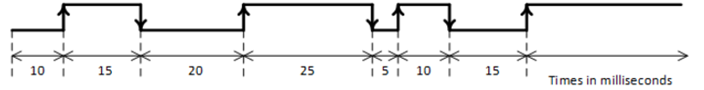 Figure 1. Incoming Signal Example Used to illustrate Input Modes
Pulse Measurements
There are two Pulse Measurements features available - High Time Pulse Measurements and Low Time Pulse Measurements. The Pulse Measurement data is stored in the FIFO Buffer.
High Time Pulse Measurements
In this input mode, the data in the FIFO buffer is the measurement for each rising transition to the next falling one. Timing measurements record the time interval (in 10 µs ticks) from a pair of transitions.
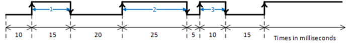 Figure 2 - High Time Pulse Measurement Input Mode
For this example, the FIFO Word Count register will be set to 3 and the FIFO Buffer Data register will contain the following three values (counts of 10 µs):
- 1500 (0x0000 05DC)
- 2500 (0x0000 09C4)
- 1000 (0x0000 03E8)
| Time Interval | Calculations | High Time Pulse Measurements |
| 1 | 1500 counts * 10 µsec = 15000 µsec = 15.0 msec | 15.0 msec |
| 2 | 2500 counts * 10 µsec = 25000 µsec = 25.0 msec | 25.0 msec |
| 3 | 1000 counts * 10 µsec = 10000 µsec = 10.0 msec | 10.0 msec |
Low Time Pulse Measurements
In this mode, the data in the FIFO buffer is the measurement for each falling edge to the next rising edge. Timing measurements record the time interval (in 10 µs ticks) from a pair of transitions.
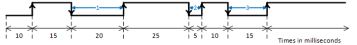 Figure 3. Low Time Pulse Measurement Input Mode
For this example, the FIFO Word Count register will be set to 3 and the FIFO Buffer Data register will contain the following three values (counts of 10 µs):
- 2000 (0x0000 07D0)
- 500 (0x0000 01F4)
- 1500 (0x0000 05DC)
| Time Interval | Calculations | Low Time Pulse Measurements |
| 1 | 2000 counts * 10 µsec = 2000 µsec = 20.0 msec | 20.0 msec |
| 2 | 500 counts * 10 µsec = 5000 µsec = 5.0 msec | 5.0 msec |
| 3 | 1500 counts * 10 µsec = 15000 µsec = 15.0 msec | 15.0 msec |
Transition Timestamps
There are three Transition Timestamp Measurements features available - Transition Timestamp for All Rising Edges, Transition Timestamp for All Falling Edges, and Transition Timestamp for All Edges. The Transition Timestamps Measurement data are store in the FIFO Buffer.
Transition Timestamp of All Rising Edges
In this mode, the data in the FIFO buffer is the Rising Edge Timestamp. The timestamp is a 32-bit counter that is incremented at the rate of 100 kHz (in other words, counter is incremented every 10 µsec). The timestamp is can be reset by the application at any time.
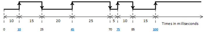 Figure 4. Transition Timestamp of All Rising Edges Input Mode
For this example, the FIFO Word Count register will be set to 4 and the FIFO Buffer Data register will contain the following four values (counts of 10 µs):
- 1000 (0x0000 03E8)
- 4500 (0x0000 1194)
- 7500 (0x0000 1D4C)
- 10000 (0x000 2710)
This data can be interpreted as follows:
| Time Interval | Calculations | Time Between Rising Edges |
| 1 to 2 | 4500 counts * 10 µsec = 35000 µsec = 35.0 msec | 35.0 msec |
| 2 to 3 | 7500 counts * 10 µsec = 30000 µsec = 30.0 msec | 30.0 msec |
| 3 to 4 | 10000 counts * 10 µsec = 25000 µsec = 25.0 msec | 25.0 msec |
Transition Timestamp of All Falling Edges
In this mode, the data in the FIFO buffer is the Falling Edge Timestamp. The timestamp is a 32-bit counter that is incremented at the rate of 100 kHz (in other words, counter is incremented every 10 µsec). The timestamp is can be reset by the application at any time.
 Figure 5. Transition Timestamp of All Falling Edges Input Mode
For this example, the FIFO Word Count register will be set to 3 and the FIFO Buffer Data register will contain the following three values (counts of 10 µs):
- 2500 (0x0000 09C4)
- 7000 (0x0000 1B58)
- 8500 (0x0000 2134)
This data can be interpreted as follows:
| Time Interval | Calculations | Time Between Falling Edges |
| 1 to 2 | 7000 - 2500 = 4500 counts = 4500 * 10 µsec = 45000 µsec = 45.0 msec | 45.0 msec |
| 2 to 3 | 8500 - 7000 = 1500 counts = 1500 * 10 µsec = 15000 µsec = 15.0 msec | 15.0 msec |
Transition Timestamp of All Edges
In this mode, the data in the FIFO buffer is the Rising and Falling Edge Timestamp. The timestamp is a 32-bit counter that is incremented at the rate of 100 kHz (in other words, counter is incremented every 10 µsec). The timestamp is can be reset by the application at any time.
 Figure 6. Transition Timestamp for All Edges Input Mode
For this example, the FIFO Word Count register will be set to 7 and the FIFO Buffer Data register will contain the following seven values (counts of 10 µs):
- 1000 (0x0000 03E8)
- 2500 (0x0000 09C4)
- 4500 (0x0000 1194)
- 7000 (0x0000 1B58)
- 7500 (0x0000 1D4C)
- 8500 (0x0000 2134)
- 10000 (0x000 2710)
This data can be interpreted as follows:
| Time Interval | Calculations | Time Between Edges |
| 1 to 2 | 2500 - 1000 = 1500 counts = 1500 * 10 µsec = 15000 µsec = 15.0 msec | 15.0 msec |
| 2 to 3 | 4500 - 2500 = 2000 counts = 2000 * 10 µsec = 20000 µsec = 20.0 msec | 20.0 msec |
| 3 to 4 | 7000 - 4500 = 2500 counts = 2500 * 10 µsec = 25000 µsec = 25.0 msec | 25.0 msec |
| 4 to 5 | 7500 - 7000 = 500 counts = 500 * 10 µsec = 5000 µsec = 5.0 msec | 5.0 msec |
| 5 to 6 | 8500 - 7500 = 1000 counts = 1000 * 10 µsec = 10000 µsec = 10.0 msec | 10.0 msec |
| 6 to 7 | 10000 - 8500 = 1500 counts = 1500 * 10 µsec = 15000 µsec = 15.0 msec | 15.0 msec |
Transition Counter
There are three Transition Counter features available - Rising Edge Transition Counter, Falling Edge Transition Counter and All Edge Transition Counter.
Rising Edges Transition Counter
In this mode, the count of the number of Rising Edges is recorded. The counter is a 32-bit counter. The counter is can be reset by the application at any time.
 Figure 7. Rising Edges Transition Counter Input Mode
For this example, the Transition Count register will be set to 4.
Falling Edges Transition Counter
In this mode, the count of the number of Falling Edges is recorded. The counter is a 32-bit counter. The counter is can be reset by the application at any time
 Figure 8. Falling Edges Transition Counter Input Mode
For this example, the Transition Count register will be set to 3.
All Edges Transition Counter
In this mode, the count of the number of Rising and Falling Edges is recorded. The counter is a 32-bit counter. The counter is can be reset by the application at any time.
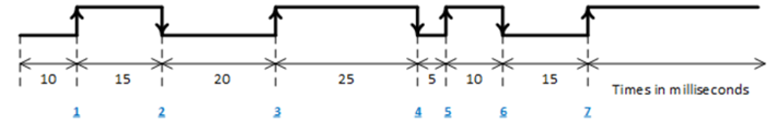 Figure 9. All Edges Transition Counter Input Mode
For this example, the Transition Count register will be set to 7.
Period Measurement
In this input mode, the data in the FIFO buffer is the measurement for each rising edge transition to the next rising edge transition. Timing measurements record the time interval (in 10 µs ticks).
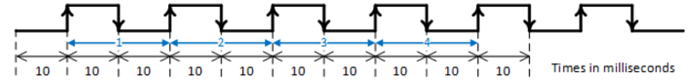 Figure 10. Period Measurement Input Mode
For this example, the FIFO Word Count register will be set to 4 and the FIFO Buffer Data register will contain the following three values (counts of 10 µs):
- 2000 (0x0000 07D0)
- 2000 (0x0000 07D0)
- 2000 (0x0000 07D0)
- 2000 (0x0000 07D0)
| Time Interval | Calculations | Period Measurements |
| 1 | 2000 counts * 10 µsec = 20000 µsec = 20.0 msec | 20.0 msec |
| 2 | 2000 counts * 10 µsec = 20000 µsec = 20.0 msec | 20.0 msec |
| 3 | 2000 counts * 10 µsec = 20000 µsec = 20.0 msec | 20.0 msec |
| 4 | 2000 counts * 10 µsec = 20000 µsec = 20.0 msec | 20.0 msec |
Frequency Measurement
In this input mode, the data in the FIFO buffer is the number of rising edge transitions for the programmable time interval programmed in the Frequency Measurement Period register.
For this example, set the Frequency Measurement Period register = 4000 (4000 * 10 µs = 40000 µs = 40 msec)
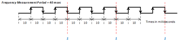 Figure 11. Frequency Measurement Input Mode
For this example, the FIFO Word Count register will be set to 3 and the FIFO Buffer Data register will contain the following three values (number of rising edges:
- 2 (0x0000 0002)
- 2 (0x0000 0002)
- 2 (0x0000 0002)
| Time Interval | Calculations | Frequency Measurements |
| 1 | 2 counts/40 msec = 2 counts/0.04 seconds = 50 Hz | 50 Hz |
| 2 | 2 counts/40 msec = 2 counts/0.04 seconds = 50 Hz | 50 Hz |
| 3 | 2 counts/40 msec = 2 counts/0.04 seconds = 50 Hz | 50 Hz |
Output Modes
There are three Enhanced Output Functionality modes: two PWM outputs and one Pattern Generator Output mode.
PWM Output
There are two PWM output modes, PWM Continuous and PWM Burst. The PWM timing is very precise with low jitter. In PWM Output mode, the Mode Select register is set to either “PWM Continuous or PWM Burst”. The value written to the PWM Period register specifies the period to output the PWM signal, the value written to the PWM Pulse Width register specifies the time for the “ON” state, and the value written to the PWM Output Polarity register specifies the initial edge of the output. For PWM Burst mode, the PWM Number of Cycles register specifies the number of cycles to output the signal. Note, there may be an initial “OFF” state level delay based on the Period time before the initial pulse is output.
PWM Continuous
Figure 12 and Figure 13 illustrate the PWM Continuous Output signal, one configured with PWM Output Polarity = Positive (0) and one configured with PWM Output Polarity = Negative (1). The configured PWM output is enabled and disabled with the Enable Measurements/Outputs register.
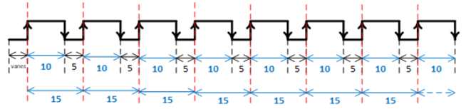 Figure 12. PWM Continuous Output (PWM Period = 15 msec, PWM Pulse Width = 10 msec, PWM Output Polarity = Positive (0))
 Figure 13. PWM Continuous Output (PWM Period = 15 msec, PWM Pulse Width = 10 msec, PWM Output Polarity = Negative (1))
PWM Burst
Figure 14 and Figure 15 illustrate the PWM Burst Output signal with the PWM Number of Cycles = 5 pulses, one configured with PWM Output Polarity = Positive (0) and one configured with PWM Output Polarity = Negative (1). The configured PWM output is enabled with the Enable Measurements/Outputs register. Once the number of pulses that were requested is outputted, the value in the Enable Measurements/Outputs register will be reset (self-clearing) to allow for the output to be re-enabled.
 Figure 14. PWM Burst Output (PWM Period = 15 msec, PWM Pulse Width = 10 msec, PWM Output Polarity = Positive (0),
PWM Number of Cycles = 5)
Figure 14. PWM Burst Output (PWM Period = 15 msec, PWM Pulse Width = 10 msec, PWM Output Polarity = Positive (0),
PWM Number of Cycles = 5)
 Figure 15. PWM Burst Output (PWM Period = 15 msec, PWM Pulse Width = 10 msec, PWM Output Polarity = Negative (1), PWM Number of Cycles = 5)
Pattern Generator
For the Pattern Generator mode, there is 64K block of unsigned 32-bit words allocated to specify the data pattern for the output channels. The data in each 32-bit word is bit-mapped per channel. The Pattern RAM Start Address and Pattern RAM End Address registers specify the starting and ending address in the 64K block to use as the data to output for each channel configured for Pattern Generator mode. The Pattern RAM Period register specifies the pattern rate. The Pattern RAM Control and Pattern RAM Number of Cycles control the Pattern Generator output - Continuous, Burst with a specified number of cycles, Pause, or External Trigger from input from Channel 1.
Note
When any channel is configured for External Trigger Pattern Generator mode, Channel 1 MUST be set as an input.
Figure 16 illustrates the output of the 24 channels for the DT4 module all configured in Pattern Generator mode
 Figure 16. Pattern Generator
REGISTER DESCRIPTIONS
The register descriptions provide the register name, Type, Data Range, Read or Write information, Initialized Value, and a description of the function.
Enhanced Input/Output Functionality Registers
The onboard Discrete I/O option provides enhanced input and output mode functionality. The Mode Select and Enable Output/Measurement registers are general control registers for the different enhanced input and output modes.
| Mode Select | |
| Function: | Configures the Enhanced Functionality Modes to apply to the channel. |
| Type: | unsigned binary word (32-bit) |
| Data Range: | See table |
| Read/Write: | R/W |
| Initialized Value: | 0 |
| Operational Settings: | It is important that the channel is correctly configured to either input or output in the Input/Output Format registers to correspond to the Enhanced Functionality Mode selected. Setting a 0 to this register will configure that channel to normal operation. |
| Mode Select Value (Decimal) | Mode Select Value (Hexadecimal) | Description |
| 0 | 0x0000 0000 | Enhanced Functionality Disabled |
| Input Enhanced Functionality Mode | ||
| 1 | 0x0000 0001 | High Time Pulse Measurements |
| 2 | 0x0000 0002 | Low Time Pulse Measurements |
| 3 | 0x0000 0003 | Transition Timestamp of All Rising Edges |
| 4 | 0x0000 0004 | Transition Timestamp of All Falling Edges |
| 5 | 0x0000 0005 | Transition Timestamp of All Edges |
| 6 | 0x0000 0006 | Rising Edges Transition Counter |
| 7 | 0x0000 0007 | Falling Edges Transition Counter |
| 8 | 0x0000 0008 | All Edges Transition Counter |
| 9 | 0x0000 0009 | Period Measurement |
| 10 | 0x0000 000A | Frequency Measurement |
| Output Enhanced Functionality Mode | ||
| 32 | 0x0000 0020 | PWM Continuous |
| 33 | 0x0000 0021 | PWM Burst |
| 34 | 0x0000 0022 | Pattern Generator |
| Enable Measurements/Outputs | |
| Function: | Enables/starts the measurements or outputs based on the Mode Select for the channel. |
| Type: | unsigned binary word (32-bit) |
| Data Range: | 0x0000 0000 to 0x00FF FFFF |
| Read/Write: | R/W |
| Initialized Value: | 0 |
| Operational Settings: | Setting the bit for the associated channel to a 1 will start the measurement or output depending on the Mode Select configuration for that channel. Setting the bit for the associated channel to 0 will stop the measurements/outputs. |
| D31 | D30 | D29 | D28 | D27 | D26 | D25 | D24 | D23 | D22 | D21 | D20 | D19 | D18 | D17 | D16 |
|---|---|---|---|---|---|---|---|---|---|---|---|---|---|---|---|
| 0 | 0 | 0 | 0 | 0 | 0 | 0 | 0 | Ch24 | Ch23 | Ch22 | Ch21 | Ch20 | Ch19 | Ch18 | Ch17 |
| D15 | D14 | D13 | D12 | D11 | D10 | D9 | D8 | D7 | D6 | D5 | D4 | D3 | D2 | D1 | D0 |
| Ch16 | Ch15 | Ch14 | Ch13 | Ch12 | Ch11 | Ch10 | Ch9 | Ch8 | Ch7 | Ch6 | Ch5 | Ch4 | Ch3 | Ch2 | Ch1 |
Input Mode Registers
After configuring the Mode Select register, write a 1 to the Reset Timer/Counter register resets the channel’s timestamp and counter used for input modes. Write a 1 to the Enable Measurements/Outputs register to begin the measurement of the input signal. Write a 0 to the Enable Measurements/Outputs register to stop the measurement of the input signal. The data can be read either while the measurements are being made on input signals or after stopping the measurements.
| Reset Timer/Counter | |
| Function: | Resets the measurement timestamp and counter for the channel. |
| Type: | unsigned binary word (32-bit) |
| Data Range: | 0x0000 0000 to 0x00FF FFFF |
| Read/Write: | W |
| Initialized Value: | 0 |
| Operational Settings: | Setting the bit for the associated channel to a 1 will: reset the timestamp used for the Pulse Measurements mode (1-2), Transition Timestamp mode (3-5), and Period Measurement mode (9) and Frequency Measurement mode (10) reset the counter used for Transition Counter mode (6-8) |
| D31 | D30 | D29 | D28 | D27 | D26 | D25 | D24 | D23 | D22 | D21 | D20 | D19 | D18 | D17 | D16 |
|---|---|---|---|---|---|---|---|---|---|---|---|---|---|---|---|
| 0 | 0 | 0 | 0 | 0 | 0 | 0 | 0 | Ch24 | Ch23 | Ch22 | Ch21 | Ch20 | Ch19 | Ch18 | Ch17 |
| D15 | D14 | D13 | D12 | D11 | D10 | D9 | D8 | D7 | D6 | D5 | D4 | D3 | D2 | D1 | D0 |
| Ch16 | Ch15 | Ch14 | Ch13 | Ch12 | Ch11 | Ch10 | Ch9 | Ch8 | Ch7 | Ch6 | Ch5 | Ch4 | Ch3 | Ch2 | Ch1 |
FIFO Registers
The FIFO registers are used for the following input modes:
- Pulse Measurements mode (1-2)
- Transition Timestamp mode (3-5)
- Period Measurement mode (9)
- Frequency Measurement mode (10)
| FIFO Buffer Data | |
| Function: | The data stored in the FIFO Buffer Data is dependent on the input mode. |
| Type: | unsigned binary word (32-bit) |
| Data Range: | 0x0000 0000 to 0xFFFF FFFF |
| Read/Write: | R |
| Initialized Value: | N/A |
| Operational Settings: | Refer to examples in Input Modes. |
| FIFO Word Count | |
| Function: | This is a counter that reports the number of 32-bit words stored in the FIFO buffer. |
| Type: | unsigned binary word (32-bit) |
| Data Range: | 0 - 255 (0x0000 0000 to 0x0000 00FF) |
| Read/Write: | R |
| Initialized Value: | 0 |
| Operational Settings: | Every time a read operation is made from the FIFO Buffer Data register, the value in the FIFO Word Count register will be decremented by one. The maximum number of words that can be stored in the FIFO is 255. |
| D31 | D30 | D29 | D28 | D27 | D26 | D25 | D24 | D23 | D22 | D21 | D20 | D19 | D18 | D17 | D16 |
|---|---|---|---|---|---|---|---|---|---|---|---|---|---|---|---|
| 0 | 0 | 0 | 0 | 0 | 0 | 0 | 0 | 0 | 0 | 0 | 0 | 0 | 0 | 0 | 0 |
| D15 | D14 | D13 | D12 | D11 | D10 | D9 | D8 | D7 | D6 | D5 | D4 | D3 | D2 | D1 | D0 |
| 0 | 0 | 0 | 0 | 0 | 0 | 0 | D | D | D | D | D | D | D | D | D |
| Clear FIFO | |
| Function: | Clears FIFO by resetting the FIFO Word Count register. |
| Type: | unsigned binary word (32-bit) |
| Data Range: | 0 or 1 |
| Read/Write: | W |
| Initialized Value: | N/A |
| Operational Settings: | Write a 1 to resets the Words in FIFO to zero; Clear FIFO register does not clear data in the buffer. A read to the buffer data will give “aged” data. |
| Bit | Description |
| D31:D1 | Reserved. Set to 0 |
| D0 | Set to 1 to reset the FIFO Word Count value to zero. |
| D31 | D30 | D29 | D28 | D27 | D26 | D25 | D24 | D23 | D22 | D21 | D20 | D19 | D18 | D17 | D16 |
|---|---|---|---|---|---|---|---|---|---|---|---|---|---|---|---|
| 0 | 0 | 0 | 0 | 0 | 0 | 0 | 0 | 0 | 0 | 0 | 0 | 0 | 0 | 0 | 0 |
| D15 | D14 | D13 | D12 | D11 | D10 | D9 | D8 | D7 | D6 | D5 | D4 | D3 | D2 | D1 | D0 |
| 0 | 0 | 0 | 0 | 0 | 0 | 0 | 0 | 0 | 0 | 0 | 0 | 0 | 0 | 0 | D |
| FIFO Status | |
| Function: | Sets the corresponding bit associated with the FIFO status type; there is a separate register for each channel. |
| Type: | unsigned binary word (32-bit) |
| Data Range: | See table |
| Read/Write: | R |
| Initialized Value: | 0 |
| Bit | Name | Description |
| D31:D4 | Reserved | Set to 0 |
| D3 | Empty | Set to 1 when FIFO Word Count = 0 |
| D2 | Almost Empty | Set to 1 when FIFO Word Count <= 63 (25%) |
| D1 | Almost Full | Set to 1 when FIFO Word Count >= 191 (75%) |
| D0 | Full | Set to 1 when FIFO Word Count = 255 |
| D31 | D30 | D29 | D28 | D27 | D26 | D25 | D24 | D23 | D22 | D21 | D20 | D19 | D18 | D17 | D16 |
|---|---|---|---|---|---|---|---|---|---|---|---|---|---|---|---|
| 0 | 0 | 0 | 0 | 0 | 0 | 0 | 0 | 0 | 0 | 0 | 0 | 0 | 0 | 0 | 0 |
| D15 | D14 | D13 | D12 | D11 | D10 | D9 | D8 | D7 | D6 | D5 | D4 | D3 | D2 | D1 | D0 |
| 0 | 0 | 0 | 0 | 0 | 0 | 0 | 0 | 0 | 0 | 0 | 0 | D | D | D | D |
Transition Count Registers
The Transition Count register are used for the following input modes:
- Transition Counter mode (6-8)
| Transition Count | |
| Function: | Contains the count of the transitions depending on the configuration in the Mode Select register - Rising Edges, Falling Edges or All Edges. |
| Type: | unsigned binary word (32-bit) |
| Data Range: | 0x0000 0000 to 0xFFFF FFFF |
| Read/Write: | R |
| Initialized Value: | 0 |
| Operational Settings: | Refer to examples in Transition Counter. |
Frequency Measurement Registers
For the Frequency Measurement mode, the period to perform the frequency measurements must be specified in the Frequency Measurement Period register.
| Frequency Measurement Period | |
| Function: | When the Mode Select register is programmed for Frequency Measurement mode (10), the value in the Frequency Measurement Period is used as the time interval for counting the number of rising edge transitions within that interval. |
| Type: | unsigned binary word (32-bit) |
| Data Range: | 0x0 to 0xFFFF FFFF |
| Read/Write: | R/W |
| Initialized Value: | 0 |
| Operational Settings: | Set the Frequency Measurement Period (LSB = 10 µs). Refer to examples in Frequency Measurement. |
Output Modes Registers
After configuring the Mode Select register, write a 1 to the Enable Measurements/Outputs register to outputting the signal. Write a 0 to the Enable Measurements/Outputs register to stop the output signal.
PWM Registers
The PWM Period, PWM Pulse Width and PWM Output Polarity registers configure the PWM output signal. When the Mode Select register is configured for PWM Burst mode, the PWM Number of Cycles register is used to specify the number of cycles to repeat for the burst.
| PWM Period | |
| Function: | When the Mode Select register is programmed for PWM Continuous or PWM Burst mode (32-33), the value in the PWM Period is used as the time interval for outputting the PWM signal. |
| Type: | unsigned binary word (32-bit) |
| Data Range: | 0x0000 0001 to 0xFFFF FFFF |
| Read/Write: | R/W |
| Initialized Value: | 0 |
| Operational Settings: | Set the PWM Period (LSB = 10 µs). The PWM Period must be greater than the value set in the PWM Pulse Width register. Refer to examples in PWM Output. |
| PWM Pulse Width | |
| Function: | When the Mode Select register is programmed for PWM Continuous or PWM Burst mode (32-33), the value in the PWM Pulse Width is used as the time interval of the “ON” state for outputting the PWM signal. |
| Type: | unsigned binary word (32-bit) |
| Data Range: | 0x0 to 0xFFFF FFFF |
| Read/Write: | R/W |
| Initialized Value: | 0 |
| Operational Settings: | Set the PWM Pulse Width (LSB = 10 µs). The PWM Pulse Width must be less than the value set in the PWM Pulse Width register. Refer to examples in PWM Output. |
| PWM Output Polarity | |
| Function: | When the Mode Select register is programmed for PWM Continuous or PWM Burst mode (32-33), the value in the PWM Output Polarity is used to specify whether the PWM output signal starts with a rising edge (Positive (0)), or a falling edge (Negative (1)). |
| Type: | unsigned binary word (32-bit) |
| Data Range: | 0x0 to 0x00FF FFFF |
| Read/Write: | R/W |
| Initialized Value: | 0 |
| Operational Settings: | The PWM Output Polarity register is used to program the starting edge of the PWM Pulse Period (rising or falling). When the PWM output Polarity is set to Positive (0), the output will start with a rising edge, when it's set to Negative (1), the output will start with a falling edge. The default is Positive (0), which is set when the PWM Polarity bit is 0. Refer to examples in PWM Output. |
| D31 | D30 | D29 | D28 | D27 | D26 | D25 | D24 | D23 | D22 | D21 | D20 | D19 | D18 | D17 | D16 |
|---|---|---|---|---|---|---|---|---|---|---|---|---|---|---|---|
| 0 | 0 | 0 | 0 | 0 | 0 | 0 | 0 | Ch24 | Ch23 | Ch22 | Ch21 | Ch20 | Ch19 | Ch18 | Ch17 |
| D15 | D14 | D13 | D12 | D11 | D10 | D9 | D8 | D7 | D6 | D5 | D4 | D3 | D2 | D1 | D0 |
| Ch16 | Ch15 | Ch14 | Ch13 | Ch12 | Ch11 | Ch10 | Ch9 | Ch8 | Ch7 | Ch6 | Ch5 | Ch4 | Ch3 | Ch2 | Ch1 |
| PWM Number of Cycles | |
| Function: | When the Mode Select register is programmed for PWM Burst mode (33), the value in the PWM Number of Cycles is used to specify the number of times to repeat the PWM output signal. |
| Type: | unsigned binary word (32-bit) |
| Data Range: | 0x0000 0001 to 0xFFFF FFFF |
| Read/Write: | R/W |
| Initialized Value: | 0 |
| Operational Settings: | Set the number of times to output the PWM signal. Refer to examples in PWM Output. |
Pattern Generator Registers
The Pattern RAM registers are a 64K block of unsigned 32-bit words allocated to specify the data pattern for the output channels. The Pattern RAM Start Address, Pattern RAM End Address, Pattern RAM Period and Pattern RAM Control registers configure the Pattern Generator output signals. When the Pattern RAM Control register is configured for Burst, the Pattern RAM Number of Cycles specify the number of cycles to repeat the pattern for the burst.
| Pattern RAM | |
| Function: | Pattern Generator Memory Block from 0x40000 to 0x7FFFC. |
| Type: | unsigned binary word (32-bit) |
| Address Range: | 0x0000 0000 to 0x00FF FFFF |
| Read/Write: R | /W |
| Initialized Value: | 0 |
| Operational Settings: | 64K block of unsigned 32-bit words. The data in each 32-bit word is bit-mapped per channel. |
| D31 | D30 | D29 | D28 | D27 | D26 | D25 | D24 | D23 | D22 | D21 | D20 | D19 | D18 | D17 | D16 |
|---|---|---|---|---|---|---|---|---|---|---|---|---|---|---|---|
| 0 | 0 | 0 | 0 | 0 | 0 | 0 | 0 | Ch24 | Ch23 | Ch22 | Ch21 | Ch20 | Ch19 | Ch18 | Ch17 |
| D15 | D14 | D13 | D12 | D11 | D10 | D9 | D8 | D7 | D6 | D5 | D4 | D3 | D2 | D1 | D0 |
| Ch16 | Ch15 | Ch14 | Ch13 | Ch12 | Ch11 | Ch10 | Ch9 | Ch8 | Ch7 | Ch6 | Ch5 | Ch4 | Ch3 | Ch2 | Ch1 |
| Pattern RAM Start Address | |
| Function: | When the Mode Select register is programmed for Pattern Generator mode (34), the Pattern RAM Start Address register specifies the starting address within the Pattern RAM block registers to use for the output. |
| Type: | unsigned binary word (32-bit) |
| Data Range: | 0x0004 0000 to 0x0007 FFFC |
| Read/Write: | R/W |
| Initialized Value: | 0 |
| Operational Settings: | The value in the Pattern RAM Start Address must be LESS than the value in the Pattern RAM End Address. |
| D31 | D30 | D29 | D28 | D27 | D26 | D25 | D24 | D23 | D22 | D21 | D20 | D19 | D18 | D17 | D16 |
|---|---|---|---|---|---|---|---|---|---|---|---|---|---|---|---|
| 0 | 0 | 0 | 0 | 0 | 0 | 0 | 0 | 0 | 0 | 0 | 0 | 0 | D | D | D |
| D15 | D14 | D13 | D12 | D11 | D10 | D9 | D8 | D7 | D6 | D5 | D4 | D3 | D2 | D1 | D0 |
| D | D | D | D | D | D | D | D | D | D | D | D | D | D | D | D |
| Pattern RAM End Address | |
| Function: | When the Mode Select register is programmed for Pattern Generator mode (34), the Pattern RAM End Address register specifies the end address within the Pattern RAM block registers to use for the output. |
| Type: | unsigned binary word (32-bit) |
| Data Range: | 0x40000 to 0x7FFFC |
| Read/Write: | R/W |
| Initialized Value: | 0 |
| Operational Settings: | The value in the Pattern RAM End Address must be GREATER than the value in the Pattern RAM Start Address. |
| D31 | D30 | D29 | D28 | D27 | D26 | D25 | D24 | D23 | D22 | D21 | D20 | D19 | D18 | D17 | D16 |
|---|---|---|---|---|---|---|---|---|---|---|---|---|---|---|---|
| 0 | 0 | 0 | 0 | 0 | 0 | 0 | 0 | 0 | 0 | 0 | 0 | 0 | D | D | D |
| D15 | D14 | D13 | D12 | D11 | D10 | D9 | D8 | D7 | D6 | D5 | D4 | D3 | D2 | D1 | D0 |
| D | D | D | D | D | D | D | D | D | D | D | D | D | D | D | D |
| Pattern RAM Period | |
| Function: | When the Mode Select register is programmed for Pattern Generator mode (34), the value in the Pattern RAM Period is used as the time interval for outputting the Pattern Generator signals. |
| Type: | unsigned binary word (32-bit) |
| Data Range: | 0x0000 0001 to 0xFFFF FFFF |
| Read/Write: | R/W |
| Initialized Value: | 0 |
| Operational Settings: | Set the Pattern RAM Period (LSB = 10 µs). |
| Pattern RAM Control | |
| Function: | When the Mode Select register is programmed for Pattern Generator mode (34), the value in the Pattern RAM Control is used to control the outputting of the Pattern Generator signals. |
| Type: | unsigned binary word (32-bit) |
| Data Range: | See table |
| Read/Write: | R/W |
| Initialized Value: | 0 |
| Operational Settings: | Configures the Pattern Generator for Continuous, Burst with a specified number of cycles, Pause, or External Trigger from input from Channel 1. |
Note
When any channel is configured for External Trigger Pattern Generator mode, Channel 1 MUST be set as an input.
| Bits | Description |
| D31-D5 | Reserved. Set to 0 |
| D4 | Falling Edge External Trigger - Channel 1 used as the input for the trigger |
| D3 | Rising Edge External Trigger - Channel 1 used as the input for the trigger |
| D2 | Pause |
| D1 | Burst Mode - value in Pattern RAM Number of Cycles register defines number of cycles to output |
| D0 | Enable Pattern Generator |
| Values | Description |
| 0x0000 | Disable Pattern Generator, Continuous Mode, No External Trigger |
| 0x0001 | Enable Pattern Generator, Continuous Mode, No External Trigger |
| 0x0002 | Disable Pattern Generator, Burst Mode, No External Trigger |
| 0x0003 | Enable Pattern Generator, Burst Mode, No External Trigger |
| 0x0005 | Enable Pattern Generator, Continuous Mode, Pause, No External Trigger |
| 0x0007 | Enable Pattern Generator, Burst Mode, Pause, No External Trigger |
| 0x0008 | Disable Pattern Generator, Continuous Mode, Rising External Trigger |
| 0x0009 | Enable Pattern Generator, Continuous Mode, Rising External Trigger |
| 0x000A | Disable Pattern Generator, Burst Mode, Rising External Trigger |
| 0x000B | Enable Pattern Generator, Burst Mode, Rising External Trigger |
| 0x000D | Enable Pattern Generator, Continuous Mode, Pause, Rising External Trigger |
| 0x000F | Enable Pattern Generator, Burst Mode, Pause, Rising External Trigger |
| 0x1000 | Disable Pattern Generator, Continuous Mode, Falling External Trigger |
| 0x1001 | Enable Pattern Generator, Continuous Mode, Falling External Trigger |
| 0x1002 | Disable Pattern Generator, Burst Mode, Falling External Trigger |
| 0x1003 | Enable Pattern Generator, Burst Mode, Falling External Trigger |
| 0x1005 | Enable Pattern Generator, Continuous Mode, Pause, Falling External Trigger |
| 0x1007 | Enable Pattern Generator, Burst Mode, Pause, Falling External Trigger |
| 0x0004, 0x0006, 0x000C, 0x000E, 0x1004, 0x1006, 0x1008-0x100F | Invalid |
| D31 | D30 | D29 | D28 | D27 | D26 | D25 | D24 | D23 | D22 | D21 | D20 | D19 | D18 | D17 | D16 |
|---|---|---|---|---|---|---|---|---|---|---|---|---|---|---|---|
| 0 | 0 | 0 | 0 | 0 | 0 | 0 | 0 | 0 | 0 | 0 | 0 | 0 | 0 | 0 | 0 |
| D15 | D14 | D13 | D12 | D11 | D10 | D9 | D8 | D7 | D6 | D5 | D4 | D3 | D2 | D1 | D0 |
| 0 | 0 | 0 | 0 | 0 | 0 | 0 | 0 | 0 | 0 | 0 | 0 | D | D | D | D |
| Pattern RAM Number of Cycles | |
| Function: | When the Mode Select register is programmed for Pattern Generator mode (34) and the Pattern RAM Control register is set for Burst mode, the value in the Pattern RAM Number of Cycles is used to specify the number of times to repeat the pattern output signal. |
| Type: | unsigned binary word (32-bit) |
| Data Range: | 0x0000 0001 to 0xFFFF FFFF |
| Read/Write: | R/W |
| Initialized Value: | 0 |
| Operational Settings: | Set the number of times to output the pattern. |
FUNCTION REGISTER MAP
Key:
| Configuration/Control |
| Status |
*When an event is detected, the bit associated with the event is set in this register and will remain set until the user clears the event bit. Clearing the bit requires writing a 1 back to the specific bit that was set when read (i.e. write-1-to-clear, writing a ‘1’ to a bit set to ‘1’ will set the bit to ‘0’).
| MODE SELECT REGISTERS | |||||
| OFFSET | REGISTER NAME | ACCESS | OFFSET | REGISTER NAME | ACCESS |
| 0x300C | Mode Select Ch 1 | R/W | |||
| 0x308C | Mode Select Ch 2 | R/W | |||
| 0x310C | Mode Select Ch 3 | R/W | |||
| 0x318C | Mode Select Ch 4 | R/W | |||
| 0x320C | Mode Select Ch 5 | R/W | |||
| 0x328C | Mode Select Ch 6 | R/W | |||
| 0x330C | Mode Select Ch 7 | R/W | |||
| 0x338C | Mode Select Ch 8 | R/W | |||
| 0x340C | Mode Select Ch 9 | R/W | |||
| 0x348C | Mode Select Ch 10 | R/W | |||
| 0x350C | Mode Select Ch 11 | R/W | |||
| 0x358C | Mode Select Ch 12 | R/W | |||
| 0x360C | Mode Select Ch 13 | R/W | |||
| 0x368C | Mode Select Ch 14 | R/W | |||
| 0x370C | Mode Select Ch 15 | R/W | |||
| 0x378C | Mode Select Ch 16 | R/W | |||
| 0x380C | Mode Select Ch 17 | R/W | |||
| 0x388C | Mode Select Ch 18 | R/W | |||
| 0x390C | Mode Select Ch 19 | R/W | |||
| 0x398C | Mode Select Ch 20 | R/W | |||
| 0x3A0C | Mode Select Ch 21 | R/W | |||
| 0x3A8C | Mode Select Ch 22 | R/W | |||
| 0x3B0C | Mode Select Ch 23 | R/W | |||
| 0x3B8C | Mode Select Ch 24 | R/W | |||
| 0x2000 | Enable Measurements/Outputs | R/W | |||
| INPUT MODES REGISTER | |||||
| OFFSET | REGISTER NAME | ACCESS | OFFSET | REGISTER NAME | ACCESS |
| 0x2004 | Reset Timer/Counter | W | |||
| FIFO REGISTERS | |||||
| OFFSET | REGISTER NAME | ACCESS | OFFSET | REGISTER NAME | ACCESS |
| 0x3000 | FIFO Buffer Data Ch 1 | R | 0x3004 | FIFO Word Count Ch 1 | R |
| 0x3080 | FIFO Buffer Data Ch 2 | R | 0x3084 | FIFO Word Count Ch 2 | R |
| 0x3100 | FIFO Buffer Data Ch 3 | R | 0x3104 | FIFO Word Count Ch 3 | R |
| 0x3180 | FIFO Buffer Data Ch 4 | R | 0x3184 | FIFO Word Count Ch 4 | R |
| 0x3200 | FIFO Buffer Data Ch 5 | R | 0x3204 | FIFO Word Count Ch 5 | R |
| 0x3280 | FIFO Buffer Data Ch 6 | R | 0x3284 | FIFO Word Count Ch 6 | R |
| 0x3300 | FIFO Buffer Data Ch 7 | R | 0x3304 | FIFO Word Count Ch 7 | R |
| 0x3380 | FIFO Buffer Data Ch 8 | R | 0x3384 | FIFO Word Count Ch 8 | R |
| 0x3400 | FIFO Buffer Data Ch 9 | R | 0x3404 | FIFO Word Count Ch 9 | R |
| 0x3480 | FIFO Buffer Data Ch 10 | R | 0x3484 | FIFO Word Count Ch 10 | R |
| 0x3500 | FIFO Buffer Data Ch 11 | R | 0x3504 | FIFO Word Count Ch 11 | R |
| 0x3580 | FIFO Buffer Data Ch 12 | R | 0x3584 | FIFO Word Count Ch 12 | R |
| 0x3600 | FIFO Buffer Data Ch 13 | R | 0x3604 | FIFO Word Count Ch 13 | R |
| 0x3680 | FIFO Buffer Data Ch 14 | R | 0x3684 | FIFO Word Count Ch 14 | R |
| 0x3700 | FIFO Buffer Data Ch 15 | R | 0x3704 | FIFO Word Count Ch 15 | R |
| 0x3780 | FIFO Buffer Data Ch 16 | R | 0x3784 | FIFO Word Count Ch 16 | R |
| 0x3800 | FIFO Buffer Data Ch 17 | R | 0x3804 | FIFO Word Count Ch 17 | R |
| 0x3880 | FIFO Buffer Data Ch 18 | R | 0x3884 | FIFO Word Count Ch 18 | R |
| 0x3900 | FIFO Buffer Data Ch 19 | R | 0x3904 | FIFO Word Count Ch 19 | R |
| 0x3980 | FIFO Buffer Data Ch 20 | R | 0x3984 | FIFO Word Count Ch 20 | R |
| 0x3A00 | FIFO Buffer Data Ch 21 | R | 0x3A04 | FIFO Word Count Ch 21 | R |
| 0x3A80 | FIFO Buffer Data Ch 22 | R | 0x3A84 | FIFO Word Count Ch 22 | R |
| 0x3B00 | FIFO Buffer Data Ch 23 | R | 0x3B04 | FIFO Word Count Ch 23 | R |
| 0x3B80 | FIFO Buffer Data Ch 24 | R | 0x3B84 | FIFO Word Count Ch 24 | R |
| 0x3008 | FIFO Status Ch 1 | R | |||
| 0x3088 | FIFO Status Ch 2 | R | |||
| 0x3108 | FIFO Status Ch 3 | R | |||
| 0x3188 | FIFO Status Ch 4 | R | |||
| 0x3208 | FIFO Status Ch 5 | R | |||
| 0x3288 | FIFO Status Ch 6 | R | |||
| 0x3308 | FIFO Status Ch 7 | R | |||
| 0x3388 | FIFO Status Ch 8 | R | |||
| 0x3408 | FIFO Status Ch 9 | R | |||
| 0x3488 | FIFO Status Ch 10 | R | |||
| 0x3508 | FIFO Status Ch 11 | R | |||
| 0x3588 | FIFO Status Ch 12 | R | |||
| 0x3608 | FIFO Status Ch 13 | R | |||
| 0x3688 | FIFO Status Ch 14 | R | |||
| 0x3708 | FIFO Status Ch 15 | R | |||
| 0x3788 | FIFO Status Ch 16 | R | |||
| 0x3808 | FIFO Status Ch 17 | R | |||
| 0x3888 | FIFO Status Ch 18 | R | |||
| 0x3908 | FIFO Status Ch 19 | R | |||
| 0x3988 | FIFO Status Ch 20 | R | |||
| 0x3A08 | FIFO Status Ch 21 | R | |||
| 0x3A88 | FIFO Status Ch 22 | R | |||
| 0x3B08 | FIFO Status Ch 23 | R | |||
| 0x3B88 | FIFO Status Ch 24 | R | |||
| 0x2008 | Reset FIFO | W | |||
| TRANSITION COUNT REGISTERS | |||||
| OFFSET | REGISTER NAME | ACCESS | OFFSET | REGISTER NAME | ACCESS |
| 0x3000 | Transition Count Ch 1 | R | |||
| 0x3080 | Transition Count Ch 2 | R | |||
| 0x3100 | Transition Count Ch 3 | R | |||
| 0x3180 | Transition Count Ch 4 | R | |||
| 0x3200 | Transition Count Ch 5 | R | |||
| 0x3280 | Transition Count Ch 6 | R | |||
| 0x3300 | Transition Count Ch 7 | R | |||
| 0x3380 | Transition Count Ch 8 | R | |||
| 0x3400 | Transition Count Ch 9 | R | |||
| 0x3480 | Transition Count Ch 10 | R | |||
| 0x3500 | Transition Count Ch 11 | R | |||
| 0x3580 | Transition Count Ch 12 | R | |||
| 0x3600 | Transition Count Ch 13 | R | |||
| 0x3680 | Transition Count Ch 14 | R | |||
| 0x3700 | Transition Count Ch 15 | R | |||
| 0x3780 | Transition Count Ch 16 | R | |||
| 0x3800 | Transition Count Ch 17 | R | |||
| 0x3880 | Transition Count Ch 18 | R | |||
| 0x3900 | Transition Count Ch 19 | R | |||
| 0x3980 | Transition Count Ch 20 | R | |||
| 0x3A00 | Transition Count Ch 21 | R | |||
| 0x3A80 | Transition Count Ch 22 | R | |||
| 0x3B00 | Transition Count Ch 23 | R | |||
| 0x3B80 | Transition Count Ch 24 | R | |||
| FREQUENCY MEASUREMENT REGISTERS | |||||
| NOTE: Base Address - 0x9010 C000 | |||||
| OFFSET | REGISTER NAME | ACCESS | OFFSET | REGISTER NAME | ACCESS |
| 0x3014 | Frequency Measurement Period Ch 1 | R/W | |||
| 0x3094 | Frequency Measurement Period Ch 2 | R/W | |||
| 0x3114 | Frequency Measurement Period Ch 3 | R/W | |||
| 0x3194 | Frequency Measurement Period Ch 4 | R/W | |||
| 0x3214 | Frequency Measurement Period Ch 5 | R/W | |||
| 0x3294 | Frequency Measurement Period Ch 6 | R/W | |||
| 0x3314 | Frequency Measurement Period Ch 7 | R/W | |||
| 0x3394 | Frequency Measurement Period Ch 8 | R/W | |||
| 0x3414 | Frequency Measurement Period Ch 9 | R/W | |||
| 0x3494 | Frequency Measurement Period Ch 10 | R/W | |||
| 0x3514 | Frequency Measurement Period Ch 11 | R/W | |||
| 0x3594 | Frequency Measurement Period Ch 12 | R/W | |||
| 0x3614 | Frequency Measurement Period Ch 13 | R/W | |||
| 0x3694 | Frequency Measurement Period Ch 14 | R/W | |||
| 0x3714 | Frequency Measurement Period Ch 15 | R/W | |||
| 0x3794 | Frequency Measurement Period Ch 16 | R/W | |||
| 0x3814 | Frequency Measurement Period Ch 17 | R/W | |||
| 0x3894 | Frequency Measurement Period Ch 18 | R/W | |||
| 0x3914 | Frequency Measurement Period Ch 19 | R/W | |||
| 0x3994 | Frequency Measurement Period Ch 20 | R/W | |||
| 0x3A14 | Frequency Measurement Period Ch 21 | R/W | |||
| 0x3A94 | Frequency Measurement Period Ch 22 | R/W | |||
| 0x3B14 | Frequency Measurement Period Ch 23 | R/W | |||
| 0x3B94 | Frequency Measurement Period Ch 24 | R/W | |||
| PWM REGISTERS | |||||
| OFFSET | REGISTER NAME | ACCESS | OFFSET | REGISTER NAME | ACCESS |
| 0x3014 | PWM Period Ch 1 | R/W | 0x3010 | PWM Pulse Width Ch 1 | R/W |
| 0x3094 | PWM Period Ch 2 | R/W | 0x3090 | PWM Pulse Width Ch 2 | R/W |
| 0x3114 | PWM Period Ch 3 | R/W | 0x3110 | PWM Pulse Width Ch 3 | R/W |
| 0x3194 | PWM Period Ch 4 | R/W | 0x3190 | PWM Pulse Width Ch 4 | R/W |
| 0x3214 | PWM Period Ch 5 | R/W | 0x3210 | PWM Pulse Width Ch 5 | R/W |
| 0x3294 | PWM Period Ch 6 | R/W | 0x3290 | PWM Pulse Width Ch 6 | R/W |
| 0x3314 | PWM Period Ch 7 | R/W | 0x3310 | PWM Pulse Width Ch 7 | R/W |
| 0x3394 | PWM Period Ch 8 | R/W | 0x3390 | PWM Pulse Width Ch 8 | R/W |
| 0x3414 | PWM Period Ch 9 | R/W | 0x3410 | PWM Pulse Width Ch 9 | R/W |
| 0x3494 | PWM Period Ch 10 | R/W | 0x3490 | PWM Pulse Width Ch 10 | R/W |
| 0x3514 | PWM Period Ch 11 | R/W | 0x3510 | PWM Pulse Width Ch 11 | R/W |
| 0x3594 | PWM Period Ch 12 | R/W | 0x3590 | PWM Pulse Width Ch 12 | R/W |
| 0x3614 | PWM Period Ch 13 | R/W | 0x3610 | PWM Pulse Width Ch 13 | R/W |
| 0x3694 | PWM Period Ch 14 | R/W | 0x3690 | PWM Pulse Width Ch 14 | R/W |
| 0x3714 | PWM Period Ch 15 | R/W | 0x3710 | PWM Pulse Width Ch 15 | R/W |
| 0x3794 | PWM Period Ch 16 | R/W | 0x3790 | PWM Pulse Width Ch 16 | R/W |
| 0x3814 | PWM Period Ch 17 | R/W | 0x3810 | PWM Pulse Width Ch 17 | R/W |
| 0x3894 | PWM Period Ch 18 | R/W | 0x3890 | PWM Pulse Width Ch 18 | R/W |
| 0x3914 | PWM Period Ch 19 | R/W | 0x3910 | PWM Pulse Width Ch 19 | R/W |
| 0x3994 | PWM Period Ch 20 | R/W | 0x3990 | PWM Pulse Width Ch 20 | R/W |
| 0x3A14 | PWM Period Ch 21 | R/W | 0x3A10 | PWM Pulse Width Ch 21 | R/W |
| 0x3A94 | PWM Period Ch 22 | R/W | 0x3A90 | PWM Pulse Width Ch 22 | R/W |
| 0x3B14 | PWM Period Ch 23 | R/W | 0x3B10 | PWM Pulse Width Ch 23 | R/W |
| 0x3B94 | PWM Period Ch 24 | R/W | 0x3B90 | PWM Pulse Width Ch 24 | R/W |
| 0x3018 | PWM Number of Cycles Ch 1 | R/W | |||
| 0x3098 | PWM Number of Cycles Ch 2 | R/W | |||
| 0x3118 | PWM Number of Cycles Ch 3 | R/W | |||
| 0x3198 | PWM Number of Cycles Ch 4 | R/W | |||
| 0x3218 | PWM Number of Cycles Ch 5 | R/W | |||
| 0x3298 | PWM Number of Cycles Ch 6 | R/W | |||
| 0x3318 | PWM Number of Cycles Ch 7 | R/W | |||
| 0x3398 | PWM Number of Cycles Ch 8 | R/W | |||
| 0x3418 | PWM Number of Cycles Ch 9 | R/W | |||
| 0x3498 | PWM Number of Cycles Ch 10 | R/W | |||
| 0x3518 | PWM Number of Cycles Ch 11 | R/W | |||
| 0x3598 | PWM Number of Cycles Ch 12 | R/W | |||
| 0x3618 | PWM Number of Cycles Ch 13 | R/W | |||
| 0x3698 | PWM Number of Cycles Ch 14 | R/W | |||
| 0x3718 | PWM Number of Cycles Ch 15 | R/W | |||
| 0x3798 | PWM Number of Cycles Ch 16 | R/W | |||
| 0x3818 | PWM Number of Cycles Ch 17 | R/W | |||
| 0x3898 | PWM Number of Cycles Ch 18 | R/W | |||
| 0x3918 | PWM Number of Cycles Ch 19 | R/W | |||
| 0x3998 | PWM Number of Cycles Ch 20 | R/W | |||
| 0x3A18 | PWM Number of Cycles Ch 21 | R/W | |||
| 0x3A98 | PWM Number of Cycles Ch 22 | R/W | |||
| 0x3B18 | PWM Number of Cycles Ch 23 | R/W | |||
| 0x3B98 | PWM Number of Cycles Ch 24 | R/W | |||
| 0x200C | PWM Output Polarity | R/W | |||
| PATTERN GENERATOR REGISTERS | |||||
| OFFSET | REGISTER NAME | ACCESS | OFFSET | REGISTER NAME | ACCESS |
| 0x0004_0000 to 0x0007_FFFC | Pattern RAM | R/W | |||
| 0x2010 | Pattern RAM Period | R/W | 0x2014 | Pattern RAM Start Address | R/W |
| 0x2018 | Pattern RAM End Address | R/W | 0x201C | Pattern RAM Control | R/W |
| 0x2020 | Pattern RAM Number of Cycles | R/W | |||
REVISION HISTORY
| Module Manual - Enhanced IO Functionality Revision History | ||
| Revision | Revision Date | Description |
| C | 2021-11-30 | C08896; Transition manual to docbuilder format - no technical info change. |
DOCS.NAII REVISIONS
| Revision Date | Description |
|---|---|
| 2026-03-02 | Formatting updates to document; no technical changes. |