RG1 DATA SHEET
Click here for the RG1 data sheet
INTRODUCTION
This module manual provides information about the North Atlantic Industries, Inc. (NAI) IRIG Timecode Receiver and Generator Function Module: RG1. This module is compatible with all latest generation NAI motherboards. The RG1 synchronizes to IRIG time codes and provides precise time in a memory register for the host SBC.
FEATURES
- IRIG Receiver; Formats A, B, G
- IRIG Generator; Formats A, B, G
- Real-Time Clock (RTC)
- Event Input Signal
- Built-in Test and Functions
PRINCIPLE OF OPERATION
The RG1 Time Code receiver synchronizes to IRIG-A/B/G time codes and provides precise time in a memory register, for the host SBC. The IRIG output of the card can be used to synchronize other IRIG time code readers. Additionally, the RG1 includes a real-time clock (RTC) that may be used as a reference source for IRIG master applications.
The most common format is IRIG-B, but the module can also support IRIG-A and IRIG-G formats as well.
The IRIG format can be configured to the user’s needs. Available features include output IRIG data streams, IRIG format, control field contents (if supported by selected IRIG format), daylight savings time, offsets, and amplitude adjustment.
Measurement
The RG1 provides precise time in a memory register through a continuously running master timer. The time information is provided in year/day/hr/min/sec/nsec/seconds-since-midnight and is subject to the selected IRIG format. The master time is derived from either an external IRIG or onboard real-time clock (RTC) reference source. A free-running time can also be applied to the master timer when an IRIG reference source is not available.
Control/Configuration
The RG1 features several attributes that can be configured to affect the behavior of the master timer including:
- IRIG protocol (B122, B123, B124, etc.)
- IRIG format (Mode A, B, or G)
- IRIG modulation (DCLS, AM ASK, or DC Manchester)
- Reference source (IRIG, local RTC)
- Free-running time (nominally for test)
- Daylight Savings Time (DST)
- Offset
- 1PPS pulse width and period settings
Capture Event
The RG1 allows the user to set the capture event time of the specified IRIG channel. The time information is provided in hr/min/sec/tenths/millisec/sub-millisec and is subject to the selected IRIG protocol and format. The capture event registers also display the current state of event input and can be configured to detect rising or falling edges.
Real Time Clock (RTC)
The RG1 includes a real-time clock (RTC) that can be used as a reference source for IRIG master applications. This feature frees the system processor from the task of updating the master timer. The RTC provides several advantages over the ‘set and forget’ functionality of the master timer.
- It provides a reference that allows for better long-term stability and reduces the potential for drift.
- A stable time reference can be set in environments where network connectivity to a time source is unavailable.
- Time will be preserved across power failures if a ‘keep-alive’ power source is provided. See DATIO19 (BKUP_PWR) in APPENDIX: PINOUT DETAILS.
The user must setup the RTC date and time before reading the master timer. Additional adjustments to the master time can be made through the daylight savings time (DST) and offset registers.
Built-In Test (BIT)/Diagnostic Capability
Automatic background BIT testing is provided. Each channel is checked for correct voltage, current and frequency. Any failure triggers an interrupt, if enabled, with the results available in the status registers. The testing is totally transparent to the user and has no effect on the operation of this module.
Status and Interrupts
The RG1 Function Module provides registers that indicate faults or events. Refer to ‘Status and Interrupts Module Manual’ for the Principle of Operation description.
Module Common Registers
The RG1 Function Module includes module common registers that provide access to module-level bare metal/FPGA revisions & compile times, unique serial number information, and temperature/voltage/current monitoring. Refer to “Module Common Registers Module Manual” for the detailed information.
REGISTER DESCRIPTIONS
The register descriptions provide the Register Name, Type, Data Range, Read or Write information, power on default initialized values, a description of the function and a data table where applicable.
Measurement Registers
Master Timer Registers
The following registers provide the Master Time in terms of Hours, Minutes, Seconds, Tenths of Seconds, Milliseconds, and Sub-millisecond. The master time is derived from either IRIG, onboard real-time clock (RTC), or Free Running time reference source.
Note
Reading the Master Time register that contains the Hours, Minutes, Seconds, and Tenths of Seconds will freeze the Master Time and Master Date registers until the next read.
Master Time (Hours, Minutes, Seconds, Tenths of Seconds)
Function: Contains the master time in hours, minutes, seconds, and tenths of seconds.
Type: unsigned binary word (32-bit) - components are in BCD format (HHMMSSTT)
Data Range: N/A
Read/Write: R
Initialized Value: Current time
Operational Settings: Reading this register will freeze the Master Time and Master Date registers until the next read.
Example: 0x1311 5214 - Hours is 13, Minutes is 11, Seconds is 52 and Tenths of Seconds is 14 (13:11:52:14).
Master Time (Hour/Minute/Seconds/Tenths of Seconds in BCD format)
| D31 | D30 | D29 | D28 | D27 | D26 | D25 | D24 | D23 | D22 | D21 | D20 | D19 | D18 | D17 | D16 |
| BCD Hours (Tens Digit) | BCD Hours (Ones Digit) | BCD Minutes (Tens Digit) | BCD Minutes (Ones Digit) | ||||||||||||
| D | D | D | D | D | D | D | D | D | D | D | D | D | D | D | D |
| D15 | D14 | D13 | D12 | D11 | D10 | D9 | D8 | D7 | D6 | D5 | D4 | D3 | D2 | D1 | D0 |
| BCD Seconds (Tens Digit) | BCD Seconds (Ones Digit) | BCD Tenths of Sec (Tens Digit) | BCD Tenths of Sec (Ones Digit) | ||||||||||||
| D | D | D | D | D | D | D | D | D | D | D | D | D | D | D | D |
Master Time (Milliseconds)
Function: Contains the master time’s millisecond component.
Type: unsigned binary word (32-bit)
Data Range: 0 - 1000 (0x0000 0000 - 0x0000 03E8)
Read/Write: R
Initialized Value: Current time
Operational Settings: The register is frozen upon a read of the Master Time (Hours, Minutes, Seconds, and Tenths of Seconds register).
Master Time (Milliseconds)
| D31 | D30 | D29 | D28 | D27 | D26 | D25 | D24 | D23 | D22 | D21 | D20 | D19 | D18 | D17 | D16 |
|---|---|---|---|---|---|---|---|---|---|---|---|---|---|---|---|
| 0 | 0 | 0 | 0 | 0 | 0 | 0 | 0 | 0 | 0 | 0 | 0 | 0 | 0 | 0 | 0 |
| D15 | D14 | D13 | D12 | D11 | D10 | D9 | D8 | D7 | D6 | D5 | D4 | D3 | D2 | D1 | D0 |
| 0 | 0 | 0 | 0 | 0 | 0 | D | D | D | D | D | D | D | D | D | D |
Master Time (Sub-Milliseconds)
Function: Contains the master time’s sub-millisecond component in steps of 8.33333 nsec.
Type: unsigned binary word (32-bit)
Data Range: 0 - 120,001 (0x0000 0000 - 0x0001 D4C1)
Read/Write: R
Initialized Value: Current time
Operational Settings: The register is frozen upon a read of the Master Time (Hours, Minutes, Seconds, and Tenths of Seconds register).
Master Time (Sub-Milliseconds)
| D31 | D30 | D29 | D28 | D27 | D26 | D25 | D24 | D23 | D22 | D21 | D20 | D19 | D18 | D17 | D16 |
|---|---|---|---|---|---|---|---|---|---|---|---|---|---|---|---|
| 0 | 0 | 0 | 0 | 0 | 0 | 0 | 0 | 0 | 0 | 0 | 0 | 0 | 0 | 0 | D |
| D15 | D14 | D13 | D12 | D11 | D10 | D9 | D8 | D7 | D6 | D5 | D4 | D3 | D2 | D1 | D0 |
| D | D | D | D | D | D | D | D | D | D | D | D | D | D | D | D |
Master Time (Seconds Since Midnight)
Function: Contains the master time’s seconds since midnight.
Type: unsigned binary word (32-bit)
Data Range: 0 - 86399 (0x0000 0000 - 0x0001 517F)
Read/Write: R
Initialized Value: Current time
Operational Settings: The register is frozen upon a read of the Master Time (Hours, Minutes, Seconds, and Tenths of Seconds register).
Master Time (Seconds Since Midnight)
| D31 | D30 | D29 | D28 | D27 | D26 | D25 | D24 | D23 | D22 | D21 | D20 | D19 | D18 | D17 | D16 |
|---|---|---|---|---|---|---|---|---|---|---|---|---|---|---|---|
| 0 | 0 | 0 | 0 | 0 | 0 | 0 | 0 | 0 | 0 | 0 | 0 | 0 | 0 | 0 | D |
| D15 | D14 | D13 | D12 | D11 | D10 | D9 | D8 | D7 | D6 | D5 | D4 | D3 | D2 | D1 | D0 |
| D | D | D | D | D | D | D | D | D | D | D | D | D | D | D | D |
Master Date
Function: Contains the master date. The master date is derived from either IRIG, onboard real-time clock (RTC), or Free Running time reference source. NOTE: the year component represents the year from 2000.
Type: unsigned binary word (32-bit) - components are in BCD format (0YYY0DDD)
Data Range: N/A
Read/Write: R
Initialized Value: Current time
Operational Settings: The register is frozen upon a read of the Master Time (Hours, Minutes, Seconds, and Tenths of Seconds register).
Example: 0x0000 0241 - Year = 0, Days in Year - 241.
Master Date (Year and Days in Year in BCD format)
| D31 | D30 | D29 | D28 | D27 | D26 | D25 | D24 | D23 | D22 | D21 | D20 | D19 | D18 | D17 | D16 |
| Zero | BCD Year (Hundreds Digit) | BCD Year (Tens Digit) | BCD Year (Ones Digit) | ||||||||||||
| 0 | 0 | 0 | 0 | D | D | D | D | D | D | D | D | D | D | D | D |
| D15 | D14 | D13 | D12 | D11 | D10 | D9 | D8 | D7 | D6 | D5 | D4 | D3 | D2 | D1 | D0 |
| Zero | BCD Day in Year (Hundreds Digit) | BCD Day in Year (Tens Digit) | BCD Day in Year (Ones Digit) | ||||||||||||
| 0 | 0 | 0 | 0 | D | D | D | D | D | D | D | D | D | D | D | D |
Actual IRIG Time Registers
The following registers provide the Actual IRIG Time in terms of Hours, Minutes, Seconds, Tenths of Seconds, Milliseconds, and Sub-millisecond. The Actual IRIG time readings are valid only if IRIG messages are being received.
Note
Reading the IRIG Time register that contains the Hours, Minutes, Seconds, and Tenths of Seconds will freeze the IRIG Time and IRIG Date registers until the next read.
Actual IRIG Time (Hours, Minutes, Seconds, Tenths of Seconds)
Function: Contains the IRIG time in hours, minutes, seconds, and tenths of seconds.
Type: unsigned binary word (32-bit) - components are in BCD format (HHMMSSTT)
Data Range: N/A
Read/Write: R
Initialized Value: Current time
Operational Settings: Reading this register will freeze the IRIG Time and IRIG Date registers until the next read.
Example: 0x1311 5214 - Hours is 13, Minutes is 11, Seconds is 52 and Tenths of Seconds is 14 (13:11:52:14).
Actual IRIG Time (Hour/Minute/Seconds/Tenths of Seconds in BCD format)
| D31 | D30 | D29 | D28 | D27 | D26 | D25 | D24 | D23 | D22 | D21 | D20 | D19 | D18 | D17 | D16 |
| BCD Hours (Tens Digit) | BCD Hours (Ones Digit) | BCD Minutes (Tens Digit) | BCD Minutes (Ones Digit) | ||||||||||||
| D | D | D | D | D | D | D | D | D | D | D | D | D | D | D | D |
| D15 | D14 | D13 | D12 | D11 | D10 | D9 | D8 | D7 | D6 | D5 | D4 | D3 | D2 | D1 | D0 |
| BCD Seconds (Tens Digit) | BCD Seconds (Ones Digit) | BCD Tenths of Sec (Tens Digit) | BCD Tenths of Sec (Ones Digit) | ||||||||||||
| D | D | D | D | D | D | D | D | D | D | D | D | D | D | D | D |
Actual IRIG Time (Seconds Since Midnight)
Function: Contains the IRIG time’s seconds since midnight.
Type: unsigned binary word (32-bit)
Data Range: 0 - 86399 (0x0000 0000 - 0x0001 517F)
Read/Write: R
Initialized Value: Current time
Operational Settings: The register is frozen upon a read of the IRIG Time (Hours, Minutes, Seconds, and Tenths of Seconds register).
Master Time (Seconds Since Midnight)
| D31 | D30 | D29 | D28 | D27 | D26 | D25 | D24 | D23 | D22 | D21 | D20 | D19 | D18 | D17 | D16 |
|---|---|---|---|---|---|---|---|---|---|---|---|---|---|---|---|
| 0 | 0 | 0 | 0 | 0 | 0 | 0 | 0 | 0 | 0 | 0 | 0 | 0 | 0 | 0 | D |
| D15 | D14 | D13 | D12 | D11 | D10 | D9 | D8 | D7 | D6 | D5 | D4 | D3 | D2 | D1 | D0 |
| D | D | D | D | D | D | D | D | D | D | D | D | D | D | D | D |
Actual IRIG Date
Function: Contains the IRIG date. The Actual IRIG date readings are valid only if IRIG messages are being received. The year component represents the year from 2000; The year counts years and cycles to the next year on January 1 of each year and will count to year 2099.
Type: unsigned binary word (32-bit) - components are in BCD format (0YYY0DDD)
Data Range: N/A
Read/Write: R
Initialized Value: Current time
*Operational Settings: The register is frozen upon a read of the Actual IRIG Time (Hours, Minutes, Seconds, and Tenths of Seconds register).
Example: 0x0000 0241 - Year = 0, Days in Year - 241.
Actual IRIG Date (Year and Days in Year in BCD format)
| D31 | D30 | D29 | D28 | D27 | D26 | D25 | D24 | D23 | D22 | D21 | D20 | D19 | D18 | D17 | D16 |
| Zero | BCD Year (Hundreds Digit) | BCD Year (Tens Digit) | BCD Year (Ones Digit) | ||||||||||||
| 0 | 0 | 0 | 0 | D | D | D | D | D | D | D | D | D | D | D | D |
| D15 | D14 | D13 | D12 | D11 | D10 | D9 | D8 | D7 | D6 | D5 | D4 | D3 | D2 | D1 | D0 |
| Zero | BCD Day in Year (Hundreds Digit) | BCD Day in Year (Tens Digit) | BCD Day in Year (Ones Digit) | ||||||||||||
| 0 | 0 | 0 | 0 | D | D | D | D | D | D | D | D | D | D | D | D |
Errored Frame Count
Function: Contains the errored received frames, based on Reference pulse positions. The errored frame count will be incremented when the received IRIG signal does not match the expected format.
Type: unsigned binary word (32-bit)
Data Range: 0 - 0xFFFF FFFF
Read/Write: R/W
Initialized Value: (errors)
Operational Settings: Write any value to clear this register.
Control/Configuration Registers
IRIG Protocol
Function: Set the IRIG Protocol with configuration settings of the IRIG Format, IRIG Modulation, Carrier Frequency and Coded Expression.
Type: unsigned binary word (32-bit)
Data Range: 0 - 0x0000 FFFF
Read/Write: R/W
Initialized Value: 0x0000 2005
Operational Settings: Setting based on the following table.
| D31..D16 | Reserved |
|---|---|
| D15..D12 | IRIG Format 1. Format A 2. Format B 7. Format G |
| D11..D8 | IRIG Modulation 0. DCLS 1. AM ASK 2. DC Manchester |
| D7..D4 | Carrier Frequency 0. No carrier 1. 100Hz 2. 1 kHz 3. 10 kHz 4. 100 kHz 5. 1 MHz |
| D3..D0 | Code Expression 0. BCDTOY, CG, SBS 1. BCDTOY, CG 2. BCDTOY 3. BCDTOY, SBS 4. BCDTOY, BCDYEAR, CF, SBS 5. BCDTOY, BCDYEAR, CF 6. BCDTOY, BCDYEAR 7. BCDTOY, BCDYEAR, SBS |
IRIG Protocol
| D31 | D30 | D29 | D28 | D27 | D26 | D25 | D24 | D23 | D22 | D21 | D20 | D19 | D18 | D17 | D16 |
| 0 | 0 | 0 | 0 | 0 | 0 | 0 | 0 | 0 | 0 | 0 | 0 | 0 | 0 | 0 | D |
| D15 | D14 | D13 | D12 | D11 | D10 | D9 | D8 | D7 | D6 | D5 | D4 | D3 | D2 | D1 | D0 |
| IRIG Format | IRIG Modulation | Carrier Frequency | Coded Expression | ||||||||||||
| D | D | D | D | D | D | D | D | D | D | D | D | D | D | D | D |
IRIG Year
Function: Contains the two-digit year for IRIG source. A value of 0xFF is set for sources that provide no year information (e.g. B122).
Type: unsigned binary word (32-bit)
Data Range: 0x00 - 0xFF
Read/Write: R/W
Initialized Value: 0xFF
Operational Settings: Specifies the two-digit year for IRIG source. For IRIG sources that have no year, this will contain the value 0xFF.
IRIG Year
| D31 | D30 | D29 | D28 | D27 | D26 | D25 | D24 | D23 | D22 | D21 | D20 | D19 | D18 | D17 | D16 |
|---|---|---|---|---|---|---|---|---|---|---|---|---|---|---|---|
| 0 | 0 | 0 | 0 | 0 | 0 | 0 | 0 | 0 | 0 | 0 | 0 | 0 | 0 | 0 | 0 |
| D15 | D14 | D13 | D12 | D11 | D10 | D9 | D8 | D7 | D6 | D5 | D4 | D3 | D2 | D1 | D0 |
| 0 | 0 | 0 | 0 | 0 | 0 | 0 | 0 | D | D | D | D | D | D | D | D |
Reference Source Registers
Reference Source
Function: Contains reference source to be used by the master timer.
Type: unsigned binary word (32-bit)
Data Range: See table
Read/Write: R/W
Initialized Value: 0
Operational Settings: Setting based on the following table:
| D31..D3 | Reserved |
|---|---|
| D2…D0 | Reference Source 0. IRIG requested 5. RTC requested (can only be requested, never preferred) 7. Free-running or No Reference |
Reference Source
| D31 | D30 | D29 | D28 | D27 | D26 | D25 | D24 | D23 | D22 | D21 | D20 | D19 | D18 | D17 | D16 |
|---|---|---|---|---|---|---|---|---|---|---|---|---|---|---|---|
| 0 | 0 | 0 | 0 | 0 | 0 | 0 | 0 | 0 | 0 | 0 | 0 | 0 | 0 | 0 | 0 |
| D15 | D14 | D13 | D12 | D11 | D10 | D9 | D8 | D7 | D6 | D5 | D4 | D3 | D2 | D1 | D0 |
| 0 | 0 | 0 | 0 | 0 | 0 | 0 | 0 | 0 | 0 | 0 | 0 | 0 | D | D | D |
Actual Reference Source
Function: Contains the actual reference source to be used by the master time.
Type: unsigned binary word (32-bit)
Data Range: See table.
Read/Write: R
Initialized Value: 0
Operational Settings: Setting based on the following table:
| D31..D3 | Reserved |
|---|---|
| D2…D0 | Actual Reference Source 0. IRIG 3. RTC (RG1 only) 5. Has never been set 6. Losing sync (coasting, possibly still okay). Coasting means that the IRIG time is deviating from the external time source. 7. Master timer can use the Free-Running time if Free-Running Launch is set. Also means No Reference if the IRIG is not incrementing (coasting, too long). |
Actual Reference Source
| D31 | D30 | D29 | D28 | D27 | D26 | D25 | D24 | D23 | D22 | D21 | D20 | D19 | D18 | D17 | D16 |
|---|---|---|---|---|---|---|---|---|---|---|---|---|---|---|---|
| 0 | 0 | 0 | 0 | 0 | 0 | 0 | 0 | 0 | 0 | 0 | 0 | 0 | 0 | 0 | 0 |
| D15 | D14 | D13 | D12 | D11 | D10 | D9 | D8 | D7 | D6 | D5 | D4 | D3 | D2 | D1 | D0 |
| 0 | 0 | 0 | 0 | 0 | 0 | 0 | 0 | 0 | 0 | 0 | 0 | 0 | D | D | D |
Free-Running Time Registers
Free-Running Time (Hours, Minutes, Seconds, Tenths of Seconds)
Function: Contains the free-running time in hours, minutes, seconds, and tenths of seconds.
Type: unsigned binary word (32-bit) - components are in BCD format (HHMMSSTT)
Data Range: N/A
Read/Write: R/W
Initialized Value: 0
Operational Settings: The free-running time will only be loaded to the master timer when the “Launch Free-Running Set” register is written to and the “Actual Reference Source” register has a value of greater than 4 which implies “has never been set”, “coasting, possibly still okay”, or “coasting, for too long”.
Free Running Time (Hour/Minute/Seconds/Tenths of Seconds in BCD format)
| D31 | D30 | D29 | D28 | D27 | D26 | D25 | D24 | D23 | D22 | D21 | D20 | D19 | D18 | D17 | D16 |
| BCD Hours (Tens Digit) | BCD Hours (Ones Digit) | BCD Minutes (Tens Digit) | BCD Minutes (Ones Digit) | ||||||||||||
| D | D | D | D | D | D | D | D | D | D | D | D | D | D | D | D |
| D15 | D14 | D13 | D12 | D11 | D10 | D9 | D8 | D7 | D6 | D5 | D4 | D3 | D2 | D1 | D0 |
| BCD Seconds (Tens Digit) | BCD Seconds (Ones Digit) | BCD Tenths of Sec (Tens Digit) | BCD Tenths of Sec (Ones Digit) | ||||||||||||
| D | D | D | D | D | D | D | D | D | D | D | D | D | D | D | D |
Free-Running Date
Function: Contains the free running date to be loaded to the master timer.
Type: unsigned binary word (32-bit) - components are in BCD format (0YYY0DDD)
Data Range: N/A
Read/Write: R/W
Initialized Value: 0
Operational Settings: The free-running date will only be loaded to the master timer when the “Launch Free-Running Set” register is written to and the “Actual Reference Source” register has a value of greater than 4 which implies “has never been set”, “coasting, possibly still okay”, or “coasting, for too long”.
Free Running Date (Year and Days in Year in BCD format)
| D31 | D30 | D29 | D28 | D27 | D26 | D25 | D24 | D23 | D22 | D21 | D20 | D19 | D18 | D17 | D16 |
| Zero | BCD Year (Hundreds Digit) | BCD Year (Tens Digit) | BCD Year (Ones Digit) | ||||||||||||
| 0 | 0 | 0 | 0 | D | D | D | D | D | D | D | D | D | D | D | D |
| D15 | D14 | D13 | D12 | D11 | D10 | D9 | D8 | D7 | D6 | D5 | D4 | D3 | D2 | D1 | D0 |
| Zero | BCD Day in Year (Hundreds Digit) | BCD Day in Year (Tens Digit) | BCD Day in Year (Ones Digit) | ||||||||||||
| 0 | 0 | 0 | 0 | D | D | D | D | D | D | D | D | D | D | D | D |
Free-Running Straight Binary Seconds (SBS)
Function: Contains the free-running straight binary seconds to be loaded to the master timer.
Type: unsigned binary word (32-bit)
Data Range: 0 - 86400 (0x0000 0000 - 0x0001 5180)
Read/Write: R/W
Initialized Value: 0
Operational Settings: The free-running SBS will only be loaded to the master timer when the “Launch Free-Running Set” register is written to and the “Actual Reference Source” register has a value of greater than 4 which implies “has never been set”, “coasting, possibly still okay”, or “coasting, for too long”.
Set Free Running SBS
| D31 | D30 | D29 | D28 | D27 | D26 | D25 | D24 | D23 | D22 | D21 | D20 | D19 | D18 | D17 | D16 |
|---|---|---|---|---|---|---|---|---|---|---|---|---|---|---|---|
| 0 | 0 | 0 | 0 | 0 | 0 | 0 | 0 | 0 | 0 | 0 | 0 | 0 | 0 | 0 | D |
| D15 | D14 | D13 | D12 | D11 | D10 | D9 | D8 | D7 | D6 | D5 | D4 | D3 | D2 | D1 | D0 |
| D | D | D | D | D | D | D | D | D | D | D | D | D | D | D | D |
Launch Free-Running Set
Function: Starts the free-running system clock
Type: unsigned binary word (32-bit)
Data Range: 0x0000 0000 - 0xFFFF FFFF
Read/Write: W
Initialized Value: 0
Operational Settings: Write any value to load the above registers to the master timer. This function only works when the Actual Reference Source (0x10e4) is greater than 4. Write only; read will always return 0xDEADDEAD.
Daylight Savings Time (DST) Registers
DST Status
Function: Contains setting whether Daylight Savings Time (DST) is in effect.
Type: unsigned binary word (32-bit)
Data Range: 0 or 1
Read/Write: R
Initialized Value: 0
Operational Settings: Reading back a 1 means DST is enabled; reading back a 0 means DST is disabled.
DST Status
| D31 | D30 | D29 | D28 | D27 | D26 | D25 | D24 | D23 | D22 | D21 | D20 | D19 | D18 | D17 | D16 |
|---|---|---|---|---|---|---|---|---|---|---|---|---|---|---|---|
| 0 | 0 | 0 | 0 | 0 | 0 | 0 | 0 | 0 | 0 | 0 | 0 | 0 | 0 | 0 | 0 |
| D15 | D14 | D13 | D12 | D11 | D10 | D9 | D8 | D7 | D6 | D5 | D4 | D3 | D2 | D1 | D0 |
| 0 | 0 | 0 | 0 | 0 | 0 | 0 | 0 | 0 | 0 | 0 | 0 | 0 | 0 | 0 | D |
DST Offset
Function: Daylight Saving Time hours and minutes adjustment to be added to reference time. Value of zero to indicate to disable DST.
Type: unsigned binary word (32-bit) - components are in BCD format (00000HMM)
Data Range: N/A
Read/Write: R/W
Initialized Value: 0
Operational Settings: BCD adjustment (in hmm) of hours/minutes to be added to reference time (0x0000 0100 in the USA). Set to 0 to disable DST.
DST Start
Function: Contains the starting value for Daylight Savings Time (DST)
Type: unsigned binary word (32-bit)
Data Range: TBD
Read/Write: R/W
Initialized Value: 0302 0200 (standard USA start)
Operational Settings: Setting based on the following table:
| D31..D24 | Month (1-12 in BCD) |
|---|---|
| D23..D20 | Day of week 0. Sunday 1. Monday 2. Tuesday 3. Wednesday 4. Thursday 5. Friday 6. Saturday |
| D19..D16 | Week number (1 to 5) |
| D15..D8 | Hour in BCD |
| D7..D0 | Minute in BCD |
DST Start
| D31 | D30 | D29 | D28 | D27 | D26 | D25 | D24 | D23 | D22 | D21 | D20 | D19 | D18 | D17 | D16 |
| BCD Month (Tens Digit) | BCD Month (Ones Digit) | Day of week | Week Number | ||||||||||||
| D | D | D | D | D | D | D | D | D | D | D | D | D | D | D | D |
| D15 | D14 | D13 | D12 | D11 | D10 | D9 | D8 | D7 | D6 | D5 | D4 | D3 | D2 | D1 | D0 |
| BCD Hours (Tens Digit) | BCD Hours (Ones Digit) | BCD Minutes (Tens Digit) | BCD Minutes (Ones Digit) | ||||||||||||
| D | D | D | D | D | D | D | D | D | D | D | D | D | D | D | D |
DST End
Function: Contains the ending value for Daylight Savings Time (DST)
Type: unsigned binary word (32-bit)
Data Range: See table
Read/Write: R/W
Initialized Value: 1101 0200
Operational Settings: TBD
| D31..D24 | Month (1-12 in BCD) |
|---|---|
| D23..D20 | Day of week 0. Sunday 1. Monday 2. Tuesday 3. Wednesday 4. Thursday 5. Friday 6. Saturday |
| D19..D16 | Week number (1 to 5) |
| D15..D8 | Hour in BCD |
| D7..D0 | Minute in BCD |
DST End
| D31 | D30 | D29 | D28 | D27 | D26 | D25 | D24 | D23 | D22 | D21 | D20 | D19 | D18 | D17 | D16 |
| BCD Month (Tens Digit) | BCD Month (Ones Digit) | Day of week | Week Number | ||||||||||||
| D | D | D | D | D | D | D | D | D | D | D | D | D | D | D | D |
| D15 | D14 | D13 | D12 | D11 | D10 | D9 | D8 | D7 | D6 | D5 | D4 | D3 | D2 | D1 | D0 |
| BCD Hours (Tens Digit) | BCD Hours (Ones Digit) | BCD Minutes (Tens Digit) | BCD Minutes (Ones Digit) | ||||||||||||
| D | D | D | D | D | D | D | D | D | D | D | D | D | D | D | D |
DCLS Propagation Offset
Function: Contains the propagation offset for IRIG when set to DCLS modulation
Type: unsigned binary word (32-bit)
Data Range: 0x0000 0000 - 0xFFFF FFFF
Read/Write: R/W
Initialized Value: 0x27
Operational Settings: Number of (8.333 ns) ticks to be added to/subtracted from received reference pulse time (+ = set in the future, - = set in the past)
Mode A Propagation Offset
Function: Contains the propagation offset for IRIG AM MODE A. Number of ticks (8.333ns) to be added or subtracted. Range = +/- 5mS.
Type: unsigned binary word (32-bit)
Data Range: 0x0000 0000 - 0xFFFF FFFF
Read/Write: R/W
Initialized Value: 0x0000 18D8
Operational Settings: Number of (8.333 ns) ticks to be added to/subtracted from received reference pulse time (+ = set in the future, - = set in the past)
Mode B Propagation Offset
Function: Contains the propagation offset for IRIG AM MODE B. Number of ticks (8.333ns) to be added or subtracted. Range = ± 5mS.
Type: unsigned binary word (32-bit)
Data Range: 0x0000 0000 - 0xFFFF FFFF
Read/Write: R/W
Initialized Value: 0x0000 F618
Operational Settings: Number of (8.333 ns) ticks to be added to/subtracted from received reference pulse time (+ = set in the future, - = set in the past)
Mode G Propagation Offset
Function: Contains the propagation offset for IRIG AM MODE G. Number of ticks (8.333ns) to be added or subtracted. Range = ± 5mS.
Type: unsigned binary word (32-bit)
Data Range: 0x0000 0000 - 0xFFFF FFFF
Read/Write: R/W
Initialized Value: 0x0000 0318
Operational Settings: Number of (8.333 ns) ticks to be added to/subtracted from received reference pulse time (+ = set in the future, - = set in the past)
Time Zone
Function: Contains the time zone offset for IRIG when set to DCLS modulation
Type: unsigned binary word (32-bit)
Data Range: ±1439
Read/Write: R/W
Initialized Value: 0
Operational Settings: Number of minutes to be added to/subtracted from received reference time to accommodate time zone differences (±1439)
IRIG Input Termination/Signal Level Registers
IRIG Input Format
Function: Contains the IRIG input format.
Type: unsigned binary word (32-bit)
Data Range: See table
Read/Write: R/W
Initialized Value: 0x0000 0003
Operational Settings: Setting based on the following table:
| D31..D3 | Reserved |
|---|---|
| D2 | Analog termination 0. Disable 1. Enable |
| D1 | Digital Input 0. RS232 1. RS485 |
| D0 | Digital termination 0. Disable 1. Enable |
IRIG Input Format
| D31 | D30 | D29 | D28 | D27 | D26 | D25 | D24 | D23 | D22 | D21 | D20 | D19 | D18 | D17 | D16 |
|---|---|---|---|---|---|---|---|---|---|---|---|---|---|---|---|
| 0 | 0 | 0 | 0 | 0 | 0 | 0 | 0 | 0 | 0 | 0 | 0 | 0 | 0 | 0 | 0 |
| D15 | D14 | D13 | D12 | D11 | D10 | D9 | D8 | D7 | D6 | D5 | D4 | D3 | D2 | D1 | D0 |
| 0 | 0 | 0 | 0 | 0 | 0 | 0 | 0 | 0 | 0 | 0 | 0 | 0 | D | D | D |
Miscellaneous Signal Levels
Function: Contains miscellaneous settings for signal level.
Type: unsigned binary word (32-bit)
Data Range: See table
Read/Write: R/W
Initialized Value: 0x0000 0003
Operational Settings: Setting based on the following table
| D31..D8 | Reserved |
|---|---|
| D7 | Serial port 1 termination 0. Not terminated 1. Terminated |
| D6 | Serial port 1 interface 0. RS232 1. RS485 |
| D5 | Reserved |
| D4 | Serial port 2 termination 0. Not terminated 1. Terminated |
| D3 | Serial port 2 interface 0. RS232 1. RS485 |
| D2 | Reserved |
| D1 | 1PPS out, Event in 0. RS232 1. RS485 |
| D0 | IRIG digital out 0. RS232 1. RS485 |
Miscellaneous Signal Levels
| D31 | D30 | D29 | D28 | D27 | D26 | D25 | D24 | D23 | D22 | D21 | D20 | D19 | D18 | D17 | D16 |
|---|---|---|---|---|---|---|---|---|---|---|---|---|---|---|---|
| 0 | 0 | 0 | 0 | 0 | 0 | 0 | 0 | 0 | 0 | 0 | 0 | 0 | 0 | 0 | 0 |
| D15 | D14 | D13 | D12 | D11 | D10 | D9 | D8 | D7 | D6 | D5 | D4 | D3 | D2 | D1 | D0 |
| 0 | 0 | 0 | 0 | 0 | 0 | 0 | 0 | D | D | D | D | D | D | D | D |
Advanced Configuration Registers
AM Output Gain
Function: Contains the AM IRIG output gain level
Type: unsigned binary word (32-bit)
Data Range: 0-255 (0x0000 - 0x00FF)
Read/Write: R/W
Initialized Value: 0x80
Operational Settings: The IRIG Gain Control for the AM IRIG Output Level.
Drift Threshold
Function: Contains the IRIG drift threshold.
Type: unsigned binary word (32-bit)
Data Range: 0-65535 (0x0000 0000 - 0x0000 FFFF)
Read/Write: R/W
Initialized Value: 0x1E
Operational Settings: The IRIG drift threshold is the number of seconds before an ‘excessive drift’ interrupt is triggered. The time is measured by comparing the master time with the actual IRIG source. The countdown starts when master time is not locked on to a reference. When the count reaches zero and the master time remains not locked on to a reference, the actual Reference source register (0x10E4) will be set to 7 (coasting for too long) and the status change in reference source (D15) in General Status register will be set.
Drift Threshold
| D31 | D30 | D29 | D28 | D27 | D26 | D25 | D24 | D23 | D22 | D21 | D20 | D19 | D18 | D17 | D16 |
|---|---|---|---|---|---|---|---|---|---|---|---|---|---|---|---|
| 0 | 0 | 0 | 0 | 0 | 0 | 0 | 0 | 0 | 0 | 0 | 0 | 0 | 0 | 0 | 0 |
| D15 | D14 | D13 | D12 | D11 | D10 | D9 | D8 | D7 | D6 | D5 | D4 | D3 | D2 | D1 | D0 |
| D | D | D | D | D | D | D | D | D | D | D | D | D | D | D | D |
Control Bits to Send
Function: Contains the IRIG user bits to send.
Type: unsigned binary word (32-bit)
Data Range: 0x0000 0000 - 0xFFFF FFFF
Read/Write: R/W
Initialized Value: 0
Operational Settings: The IRIG user bits to send are loaded at the beginning of an IRIG Tx frame.
Control Bits Received
Function: Contains the IRIG user bits received.
Type: unsigned binary word (32-bit)
Data Range: 0x0000 0000 - 0xFFFF FFFF
Read/Write: R/W
Initialized Value: 0
Operational Settings: This applies to both analog and digital IRIG. Not all IRIG protocol supports user bits (CF) field.
1PPS Pulse Width
Function: Contains the 1PPS Pulse Width for the specified IRIG channel in units of microseconds. The default is 10 msec and its base unit is 1 uS.
Type: unsigned binary word (32-bit)
Data Range: 0x0000 0000 - 0xFFFF FFFF
Read/Write: R/W
Initialized Value: 10,000 (0x0000 2710)
Operational Settings: The 1PPS pulse is generated by the master timer. Output only.
Periodic Interrupt Period
Function: Contains the periodic interrupt period of 1PPS signal. The default is 1 second and its base unit is 1 uS.
Type: unsigned binary word (32-bit)
Data Range: 0x0000 0000 - 0xFFFF FFFF
Read/Write: R/W
Initialized Value: 1,000,000 (0x000F 4240)
Operational Settings: The 1PPS pulse is generated by the master timer. Output only.
Capture Event Registers
Capture Event Time (Hours, Minutes, Seconds, Tenths of Seconds)
Function: Contains the capture event time in hours, minutes, seconds, and tenths of seconds.
Type: unsigned binary word (32-bit) - components are in BCD format (HHMMSSTT)
Data Range: N/A
Read/Write: R/W
Initialized Value: last edge
Operational Settings: Write any value to re-arm the capture. NOTE: B122 protocol format: HHMMSS00
Capture Event Time (Hour/Minute/Seconds/Tenths of Seconds in BCD format)
| D31 | D30 | D29 | D28 | D27 | D26 | D25 | D24 | D23 | D22 | D21 | D20 | D19 | D18 | D17 | D16 |
| BCD Hours (Tens Digit) | BCD Hours (Ones Digit) | BCD Minutes (Tens Digit) | BCD Minutes (Ones Digit) | ||||||||||||
| D | D | D | D | D | D | D | D | D | D | D | D | D | D | D | D |
| D15 | D14 | D13 | D12 | D11 | D10 | D9 | D8 | D7 | D6 | D5 | D4 | D3 | D2 | D1 | D0 |
| BCD Seconds (Tens Digit) | BCD Seconds (Ones Digit) | BCD Tenths of Sec (Tens Digit) | BCD Tenths of Sec (Ones Digit) | ||||||||||||
| D | D | D | D | D | D | D | D | D | D | D | D | D | D | D | D |
Capture Event Time (Milliseconds)
Function: Contains the capture event time’s millisecond component.
Type: unsigned binary word (32-bit)
Data Range: 0 - 1000 (0x0000 0000 - 0x0000 03E8)
Read/Write: R
Initialized Value: 0
Operational Settings: This is the time of last edge of EVENT input in milliseconds.
Capture Event Time (Milliseconds)
| D31 | D30 | D29 | D28 | D27 | D26 | D25 | D24 | D23 | D22 | D21 | D20 | D19 | D18 | D17 | D16 |
|---|---|---|---|---|---|---|---|---|---|---|---|---|---|---|---|
| 0 | 0 | 0 | 0 | 0 | 0 | 0 | 0 | 0 | 0 | 0 | 0 | 0 | 0 | 0 | 0 |
| D15 | D14 | D13 | D12 | D11 | D10 | D9 | D8 | D7 | D6 | D5 | D4 | D3 | D2 | D1 | D0 |
| 0 | 0 | 0 | 0 | 0 | 0 | D | D | D | D | D | D | D | D | D | D |
Capture Event Time (Sub-Milliseconds)
Function: Contains the capture event time’s sub-millisecond component in steps of 8.33333 nsec.
Type: unsigned binary word (32-bit)
Data Range: 0 - 120,001 (0x0000 0000 - 0x0001 D4C1)
Read/Write: R
Initialized Value: 0
Operational Settings: This is the time of last edge of EVENT input in sub-milliseconds.
Capture Event Time (Sub-Milliseconds)
| D31 | D30 | D29 | D28 | D27 | D26 | D25 | D24 | D23 | D22 | D21 | D20 | D19 | D18 | D17 | D16 |
|---|---|---|---|---|---|---|---|---|---|---|---|---|---|---|---|
| 0 | 0 | 0 | 0 | 0 | 0 | 0 | 0 | 0 | 0 | 0 | 0 | 0 | 0 | 0 | D |
| D15 | D14 | D13 | D12 | D11 | D10 | D9 | D8 | D7 | D6 | D5 | D4 | D3 | D2 | D1 | D0 |
| D | D | D | D | D | D | D | D | D | D | D | D | D | D | D | D |
Capture Event Edge
Function: Contains the Capture Event Rising (0) or Falling (1) Edge Detect type. Also displays the current state of EVENT input.
Type: unsigned binary word (32-bit)
Data Range: See table
Read/Write: R/W
Initialized Value: 0
Operational Settings: Set bit to 0 for rising edge detect, or to 1 for falling edge detect.
| D31 | Current State of event input |
|---|---|
| D30..D1 | Reserved |
| D0 | Edge detect 0. Rising edge 1. Falling edge |
Capture Event Edge
| D31 | D30 | D29 | D28 | D27 | D26 | D25 | D24 | D23 | D22 | D21 | D20 | D19 | D18 | D17 | D16 |
|---|---|---|---|---|---|---|---|---|---|---|---|---|---|---|---|
| 0 | 0 | 0 | 0 | 0 | 0 | 0 | 0 | 0 | 0 | 0 | 0 | 0 | 0 | 0 | 0 |
| D15 | D14 | D13 | D12 | D11 | D10 | D9 | D8 | D7 | D6 | D5 | D4 | D3 | D2 | D1 | D0 |
| 0 | 0 | 0 | 0 | 0 | 0 | 0 | 0 | 0 | 0 | 0 | 0 | 0 | 0 | 0 | D |
Real Time Clock (RTC) Registers
RTC Time
Function: Contains the RTC time in hours, minutes, and seconds.
Type: unsigned binary word (32-bit) - components are in BCD format (00HHMMSS)
Data Range: N/A
Read/Write: R/W
Initialized Value: 0
Operational Settings: Write this first before writing to other Real Time Clock setting. Once the RTC Time is set, write to the RTC Control register.
Real Time Clock Time (Hour/Minute/Seconds/Tenths of Seconds in BCD format)
| D31 | D30 | D29 | D28 | D27 | D26 | D25 | D24 | D23 | D22 | D21 | D20 | D19 | D18 | D17 | D16 |
| Zero | Zero | BCD Hour (Tens Digit) | BCD Hour (Ones Digit) | ||||||||||||
| D | D | D | D | D | D | D | D | D | D | D | D | D | D | D | D |
| D15 | D14 | D13 | D12 | D11 | D10 | D9 | D8 | D7 | D6 | D5 | D4 | D3 | D2 | D1 | D0 |
| BCD Seconds (Tens Digit) | BCD Seconds (Ones Digit) | BCD Tenths of Sec (Tens Digit) | BCD Tenths of Sec (Ones Digit) | ||||||||||||
| D | D | D | D | D | D | D | D | D | D | D | D | D | D | D | D |
RTC Date
Function: Sets the RTC date in days, months, and years.
Type: unsigned binary word (32-bit) - components are in BCD format (00DDMMYY)
Data Range: N/A
Read/Write: R/W
Initialized Value: 0
Operational Settings: Write this first before writing to other Real Date Clock setting. Once the RTC Date is set, write to the RTC Control register.
RTC Date (Days, Month and Year in BCD format)
| D31 | D30 | D29 | D28 | D27 | D26 | D25 | D24 | D23 | D22 | D21 | D20 | D19 | D18 | D17 | D16 |
| Zero | Zero | BCD Hour (Tens Digit) | BCD Hour (Ones Digit) | ||||||||||||
| D | D | D | D | D | D | D | D | D | D | D | D | D | D | D | D |
| D15 | D14 | D13 | D12 | D11 | D10 | D9 | D8 | D7 | D6 | D5 | D4 | D3 | D2 | D1 | D0 |
| BCD Month (Tens Digit) | BCD Month (Ones Digit) | BCD Year (Tens Digit) | BCD Year (Ones Digit) | ||||||||||||
| D | D | D | D | D | D | D | D | D | D | D | D | D | D | D | D |
RTC Control
Function: Contains the RTC Control.
Type: unsigned binary word (32-bit)
Data Range: See table
Read/Write: R/W
Initialized Value: 0
Operational Settings: Settings based on the following table:
| D31 | State of 1 Hz pin |
|---|---|
| D30..D1 | Reserved |
| D0 | Ready to set RTC Time/Date (write to this bit after bit goes high to set) |
RTC Control
| D31 | D30 | D29 | D28 | D27 | D26 | D25 | D24 | D23 | D22 | D21 | D20 | D19 | D18 | D17 | D16 |
|---|---|---|---|---|---|---|---|---|---|---|---|---|---|---|---|
| 0 | 0 | 0 | 0 | 0 | 0 | 0 | 0 | 0 | 0 | 0 | 0 | 0 | 0 | 0 | 0 |
| D15 | D14 | D13 | D12 | D11 | D10 | D9 | D8 | D7 | D6 | D5 | D4 | D3 | D2 | D1 | D0 |
| 0 | 0 | 0 | 0 | 0 | 0 | 0 | 0 | 0 | 0 | 0 | 0 | 0 | 0 | 0 | D |
RTC Propagation Offset
Function: Contains the propagation offset for the RTC
Type: unsigned binary word (32-bit)
Data Range: 0x0000 0000 - 0xFFFF FFFF
Read/Write: R/W
Initialized Value: 0x12
Operational Settings: Number of (8.333 ns) ticks to be added to/subtracted from received reference pulse time (+ = set in the future, - = set in the past).
RTC Time Zone Offset
Function: Contains the time zone offset for the RTC
Type: unsigned binary word (32-bit)
Data Range: ±1439
Read/Write: R/W
Initialized Value: 0
Operational Settings: Number of minutes to be added to/subtracted from received reference time to accommodate time zone differences (±1439).
Module Common Registers
Refer to “Module Common Registers Module Manual” for the register descriptions.
Status and Interrupt Registers
The RG1 Module provides status registers for BIT and General Interrupts.
BIT Status
There are four registers associated with the BIT Status: Dynamic, Latched, Interrupt Enable, and Set Edge/Level Interrupt. The BIT Status register will indicate an error when there is a software fault.
| D31..D2 | Reserved |
|---|---|
| D1 | (software fault) |
| D0 | Reserved |
BIT Status
| BIT Dynamic Status | |||||||||||||||
| BIT Latched Status | |||||||||||||||
| BIT Interrupt Enable | |||||||||||||||
| BIT Set Edge/Level Interrupt | |||||||||||||||
| D31 | D30 | D29 | D28 | D27 | D26 | D25 | D24 | D23 | D22 | D21 | D20 | D19 | D18 | D17 | D16 |
| 0 | 0 | 0 | 0 | 0 | 0 | 0 | 0 | 0 | 0 | 0 | 0 | 0 | 0 | 0 | 0 |
| D15 | D14 | D13 | D12 | D11 | D10 | D9 | D8 | D7 | D6 | D5 | D4 | D3 | D2 | D1 | D0 |
| 0 | 0 | 0 | 0 | 0 | 0 | 0 | 0 | 0 | 0 | 0 | 0 | 0 | 0 | D | 0 |
Function: Sets the corresponding bit associated with the channel’s BIT error.
Type: unsigned binary word (32-bit)
Data Range: 0x0000 0000 to 0x0000 000F
Read/Write: R (Dynamic), R/W (Latched, Interrupt Enable, Edge/Level Interrupt)
Initialized Value: 0
Note
BIT Status is part of background testing, and the status register may be checked or polled at any given time.
General Interrupts Status
There are four registers associated with the General Interrupts Status: Dynamic, Latched, Interrupt Enable, and Set Edge/Level Interrupt. The General Interrupts Status register will indicate an error when there is a change in an RG1 status.
| D31 | Test interrupt - can be written high or low |
|---|---|
| D30 | Did a DST adjust |
| D29 | Programmable-duration user interrupt (ref: 0x1164) |
| D28..D21 | Reserved |
| D20 | Event detected |
| D19..D16 | Reserved |
| D15 | Change in reference source |
| D14..D8 | Reserved |
| D7 | Control bits received |
| D6 | Received control bits changed |
| D5 | Interrupt on 1PPS output going high |
| D4 | IRIG reference pulse received |
| D3..D2 | Reserved |
| D1 | Receiving IRIG reference |
| D0 | IRIG reference loss |
General Interrupt Status
| General Interrupts Dynamic Status | |||||||||||||||
| General Interrupts Latched Status | |||||||||||||||
| General Interrupts Interrupt Enable | |||||||||||||||
| General Interrupts Set Edge/Level Interrupt | |||||||||||||||
| D31 | D30 | D29 | D28 | D27 | D26 | D25 | D24 | D23 | D22 | D21 | D20 | D19 | D18 | D17 | D16 |
| D | D | D | 0 | 0 | 0 | 0 | 0 | 0 | 0 | 0 | D | 0 | 0 | 0 | 0 |
| D15 | D14 | D13 | D12 | D11 | D10 | D9 | D8 | D7 | D6 | D5 | D4 | D3 | D2 | D1 | D0 |
| D | 0 | 0 | 0 | 0 | 0 | 0 | 0 | D | D | D | D | 0 | 0 | D | D |
Function: Sets the corresponding bit associated with the channel’s General Interrupt status.
Type: unsigned binary word (32-bit)
Data Range: 0x0000 0000 to 0x0000 000F
Read/Write: R (Dynamic), R/W (Latched, Interrupt Enable, Edge/Level Interrupt)
Initialized Value:
Dynamic Status (0x810): 0x0010 0002
Latched Status (0x814): 0x2010 80B3
Interrupt Enable (0x818): 0x0000 0000
Edge/Level Interrupt (0x81C): 0x0000 0000
Interrupt Vector and Steering
When interrupts are enabled, the interrupt vector associated with the specific interrupt can be programmed (typically with a unique number/identifier) such that it can be utilized in the Interrupt Service Routine (ISR) to identify the type of interrupt. When an interrupt occurs, the contents of the Interrupt Vector registers is reported as part of the interrupt mechanism. In addition to specifying the interrupt vector, the interrupt can be directed (“steered”) to the native bus or to the application running on the onboard ARM processor.
Note
The Interrupt Vector and Interrupt Steering registers are mapped to the Motherboard Common Memory and these registers are associated with the Module Slot position (refer to Function Register Map).
Interrupt Vector Function: Set an identifier for the interrupt. Type: unsigned binary word (32-bit) Data Range: 0x0000 0000 to 0xFFFF FFFF Read/Write: R/W Initialized Value: 0 Operational Settings: When an interrupt occurs, this value is reported as part of the interrupt mechanism.
Interrupt Steering Function: Sets where to direct the interrupt. Type: unsigned binary word (32-bit) Data Range: See table Read/Write: R/W Initialized Value: 0 Operational Settings: When an interrupt occurs, the interrupt is sent as specified: Link to original
Direct Interrupt to VME 1 Direct Interrupt to ARM Processor (via SerDes) +
(Custom App on ARM or NAI Ethernet Listener App)2 Direct Interrupt to PCIe Bus 5 Direct Interrupt to cPCI Bus 6
FUNCTION REGISTER MAP
Key:
Bold Italic = Configuration/Control
Bold Underline = Measurement/Status
Measurement Registers
Master Time/Date Registers
| 0x1000 | Master Time (Hours, Minutes, Seconds, Tenths of Second) | R |
|---|---|---|
| 0x1008 | Master Time (Milliseconds) | R |
| 0x1010 | Master Time (Sub-Milliseconds) | R |
| 0x1014 | Master Time (Seconds Since Midnight) | R |
| 0x1004 | Master Date | R |
Actual IRIG Time Registers
| 0x1280 | Actual IRIG Time (Hours, Minutes, Seconds, Tenths of Second) | R |
|---|---|---|
| 0x1290 | Actual IRIG Time (Seconds Since Midnight) | R |
| 0x1284 | Actual IRIG Date | R |
| 0x12F8 | Errored Frame Count | R/W |
Control/Configuration Registers
IRIG Protocol/Year
| 0x1100 | IRIG Protocol | R/W |
|---|---|---|
| 0x106C | IRIG Year | R/W |
Reference Source Registers
| 0x10E0 | Reference Source | R/W |
|---|---|---|
| 0x10E4 | Actual Reference Source | R |
Free-Running Time Registers
| 0x1020 | Free-Running Time | R/W |
|---|---|---|
| 0x1024 | Free-Running Date | R/W |
| 0x1028 | Free-Running SBS | R/W |
| 0x102C | Launch Free-Running Set | R/W |
Daylight Savings Time (DST) Registers
| 0x1030 | DST Status | R |
|---|---|---|
| 0x1140 | DST Offset | R/W |
| 0x1144 | DST Start | R/W |
| 0x1148 | DST End | R/W |
| 0x1120 | DCLS Propagation Offset | R/W |
| 0x1154 | Mode A Propagation Offset | R/W |
| 0x1158 | Mode B Propagation Offset | R/W |
| 0x115C | Mode G Propagation Offset | R/W |
| 0x1124 | Time Zone | R/W |
IRIG Input Termination/Signal Level Registers
| 0x1168 | IRIG Input Format | R/W |
|---|---|---|
| 0x1114 | Miscellaneous Signal Levels | R/W |
Advanced Configuration Registers
| 0x1080 | AM Output Gain | R/W |
|---|---|---|
| 0x10B4 | Drift Threshold | R/W |
| 0x1090 | Control Bits to Send | R/W |
| 0x1094 | Control Bits Received | R |
| 0x1160 | 1PPS Pulse Width | R/W |
| 0x1164 | Periodic Interrupt Period | R/W |
Capture Event Registers
| 0x1070 | Capture Event (Hours, Minutes, Seconds, Tenths of Second) | R/W |
|---|---|---|
| 0x1074 | Capture Event Time (Millisecond) | R |
| 0x1078 | Capture Event Time (Sub- Millisecond) | R |
| 0x107C | Capture Event Edge | R/W |
Real Time Clock (RTC) Registers
| 0x1380 | RTC Time (Hours, Minutes, Seconds, Tenths of Second) | R/W |
|---|---|---|
| 0x1384 | RTC Date | R/W |
| 0x1388 | RTC Control | R/W |
| 0x1130 | RTC Propagation Offset | R/W |
| 0x1134 | RTC Time Zone Offset | R/W |
Status Registers
BIT Status
| 0x0800 | Dynamic Status | R |
|---|---|---|
| 0x0804 | Latched Status* | R/W |
| 0x0808 | Interrupt Enable | R/W |
| 0x080C | Set Edge/Level Interrupt | R/W |
General Status Registers
| 0x0810 | Dynamic Status | R |
|---|---|---|
| 0x0814 | Latched Status* | R/W |
| 0x0818 | Interrupt Enable | R/W |
| 0x081C | Set Edge/Level Interrupt | R/W |
Interrupt Registers
The Interrupt Vector and Interrupt Steering registers are located on the Motherboard Memory Space and do not require any Module Address Offsets. These registers are accessed using the absolute addresses listed in the table below.
| 0x0500 | Module 1 Interrupt Vector 1 - BIT | R/W |
|---|---|---|
| 0x0504 | Module 1 Interrupt Vector 2 - General | R/W |
| 0x0508 to 0x057C | Module 1 Interrupt Vector 3 - 32 - Reserved | R/W |
| 0x0600 | Module 1 Interrupt Steering 1 - BIT | R/W |
|---|---|---|
| 0x0604 | Module 1 Interrupt Steering 2 - General | R/W |
| 0x0608 to 0x067C | Module 1 Interrupt Steering 3 - 32 - Reserved | R/W |
| 0x0700 | Module 2 Interrupt Vector 1 - BIT | R/W |
|---|---|---|
| 0x0704 | Module 2 Interrupt Vector 2 - General | R/W |
| 0x0708 to 0x077C | Module 2 Interrupt Vector 3 - 32 - Reserved | R/W |
| 0x0800 | Module 2 Interrupt Steering 1 - BIT | R/W |
|---|---|---|
| 0x0804 | Module 2 Interrupt Steering 2 - General | R/W |
| 0x0808 to 0x087C | Module 2 Interrupt Steering 3 - 32 - Reserved | R/W |
| 0x0900 | Module 3 Interrupt Vector 1 - BIT | R/W |
|---|---|---|
| 0x0904 | Module 3 Interrupt Vector 2 - General | R/W |
| 0x0908 to 0x097C | Module 3 Interrupt Vector 3 - 32 - Reserved | R/W |
| 0x0A00 | Module 3 Interrupt Steering 1 - BIT | R/W |
|---|---|---|
| 0x0A04 | Module 3 Interrupt Steering 2 - General | R/W |
| 0x0A08 to 0x0A7C | Module 3 Interrupt Steering 3 - 32 - Reserved | R/W |
| 0x0B00 | Module 4 Interrupt Vector 1 - BIT | R/W |
|---|---|---|
| 0x0B04 | Module 4 Interrupt Vector 2 - General | R/W |
| 0x0B08 to 0x0B7C | Module 4 Interrupt Vector 3 - 32 - Reserved | R/W |
| 0x0C00 | Module 4 Interrupt Steering 1 - BIT | R/W |
|---|---|---|
| 0x0C04 | Module 4 Interrupt Steering 2 - General | R/W |
| 0x0C08 to 0x0C7C | Module 4 Interrupt Steering 3 - 32 - Reserved | R/W |
| 0x0D00 | Module 5 Interrupt Vector 1 - BIT | R/W |
|---|---|---|
| 0x0D04 | Module 5 Interrupt Vector 2 - General | R/W |
| 0x0D08 to 0x0D7C | Module 5 Interrupt Vector 3 - 32 - Reserved | R/W |
| 0x0E00 | Module 5 Interrupt Steering 1 - BIT | R/W |
|---|---|---|
| 0x0E04 | Module 5 Interrupt Steering 2 - General | R/W |
| 0x0E08 to 0x0E7C | Module 5 Interrupt Steering 3 - 32 - Reserved | R/W |
| 0x0F00 | Module 6 Interrupt Vector 1 - BIT | R/W |
|---|---|---|
| 0x0F04 | Module 6 Interrupt Vector 2 - General | R/W |
| 0x0F08 to 0x0F7C | Module 6 Interrupt Vector 3 - 32 - Reserved | R/W |
| 0x1000 | Module 6 Interrupt Steering 1 - BIT | R/W |
|---|---|---|
| 0x1004 | Module 6 Interrupt Steering 2 - General | R/W |
| 0x1008 to 0x107C | Module 6 Interrupt Steering 3 - 32 - Reserved | R/W |
APPENDIX: PIN-OUT DETAILS
Pin-out details (for reference) are shown below, with respect to DATAIO. Additional information on pin-outs can be found in the Motherboard Operational Manuals
| Module Signal (Ref Only) | 44-Pin I/O | 50-Pin I/O (Mod Slot 1-J3) | 50-Pin I/O (Mod Slot 2-J4) | 50-Pin I/O (Mod Slot 3-J3) | 50-Pin I/O (Mod Slot 3-J4) | IRIG (RG1)* |
|---|---|---|---|---|---|---|
| DATIO1 | 2 | 10 | 1 | 2 | ||
| DATIO2 | 24 | 35 | 26 | 27 | ||
| DATIO3 | 3 | 11 | 2 | 3 | ||
| DATIO4 | 25 | 36 | 27 | 28 | ||
| DATIO5 | 5 | 13 | 4 | 5 | ||
| DATIO6 | 27 | 38 | 29 | 30 | ||
| DATIO7 | 7 | 14 | 5 | 6 | ||
| DATIO8 | 29 | 39 | 30 | 31 | ||
| DATIO9 | 8 | 15 | 6 | 7 | ||
| DATIO10 | 30 | 40 | 31 | 32 | ||
| DATIO11 | 10 | 17 | 8 | 9 | ||
| DATIO12 | 32 | 42 | 33 | 34 | ||
| DATIO13 | 12 | 18 | 9 | 17 | ||
| DATIO14 | 34 | 43 | 34 | 42 | 1PPS_OUTp / 1PPS_OUT | |
| DATIO15 | 13 | 19 | 10 | 18 | IRIG_DI_INn | |
| DATIO16 | 35 | 44 | 35 | 43 | IRIG_DI_INp / IRIG_DI_IN | |
| DATIO17 | 15 | 21 | 12 | 20 | EVENT_INn | |
| DATIO18 | 37 | 46 | 37 | 45 | EVENT_INp / EVENT_IN | |
| DATIO19 | 17 | 22 | 13 | 21 | BKUP_PWR** | |
| DATIO20 | 39 | 47 | 38 | 46 | ISO_GND | |
| DATIO21 | 18 | 23 | 14 | 22 | IRIG_DI_OUTn | |
| DATIO22 | 40 | 48 | 39 | 47 | IRIG_DI_OUTp / IRIG_DI_OUT | |
| DATIO23 | 20 | 25 | 16 | 24 | IRIG_AN_IN | |
| DATIO24 | 42 | 50 | 41 | 49 | IRIG_AN_IRET | |
| DATIO25 | 4 | 12 | 3 | 4 | ||
| DATIO26 | 26 | 37 | 28 | 29 | ||
| DATIO27 | 9 | 16 | 7 | 8 | 10_MHZn_OUT | |
| DATIO28 | 31 | 41 | 32 | 33 | 10_MHZp_OUT | |
| DATIO29 | 14 | 20 | 11 | 19 | GPIO0_INn | |
| DATIO30 | 36 | 45 | 36 | 44 | GPIO0_INp / GPIO0_IN | |
| DATIO31 | 19 | 24 | 15 | 23 | IRIG_AN_OUT | |
| DATIO32 | 41 | 49 | 40 | 48 | IRIG_AN_ORET | |
| DATIO33 | 6 | |||||
| DATIO34 | 28 | |||||
| DATIO35 | 11 | |||||
| DATIO36 | 33 | |||||
| DATIO37 | 16 | |||||
| DATIO38 | 38 | |||||
| DATIO39 | 21 | |||||
| DATIO40 | 43 | |||||
| N/A |
NOTES:
*RS-485 requires connections to both positive (p) and negative (n) signals. RS-232 requires connection to just the positive (p) signal. ISO_GND: signal return for the IRIG DCLS signal input (Digital IRIG-In Line Receiver) in RS-232 interface mode.
**The RTC backup voltage can range from 1.8 to 5.5V.
STATUS AND INTERRUPTS
Status registers indicate the detection of faults or events. The status registers can be channel bit-mapped or event bit-mapped. An example of a channel bit-mapped register is the BIT status register, and an example of an event bit-mapped register is the FIFO status register.
For those status registers that allow interrupts to be generated upon the detection of the fault or the event, there are four registers associated with each status: Dynamic, Latched, Interrupt Enabled, and Set Edge/Level Interrupt.
Dynamic Status: The Dynamic Status register indicates the current condition of the fault or the event. If the fault or the event is momentary, the contents in this register will be clear when the fault or the event goes away. The Dynamic Status register can be polled, however, if the fault or the event is sporadic, it is possible for the indication of the fault or the event to be missed.
Latched Status: The Latched Status register indicates whether the fault or the event has occurred and keeps the state until it is cleared by the user. Reading the Latched Status register is a better alternative to polling the Dynamic Status register because the contents of this register will not clear until the user commands to clear the specific bit(s) associated with the fault or the event in the Latched Status register. Once the status register has been read, the act of writing a 1 back to the applicable status register to any specific bit (channel/event) location will “clear” the bit (set the bit to 0). When clearing the channel/event bits, it is strongly recommended to write back the same bit pattern as read from the Latched Status register. For example, if the channel bit-mapped Latched Status register contains the value 0x0000 0005, which indicates fault/event detection on channel 1 and 3, write the value 0x0000 0005 to the Latched Status register to clear the fault/event status for channel 1 and 3. Writing a “1” to other channels that are not set (example 0x0000 000F) may result in incorrectly “clearing” incoming faults/events for those channels (example, channel 2 and 4).
Interrupt Enable: If interrupts are preferred upon the detection of a fault or an event, enable the specific channel/event interrupt in the Interrupt Enable register. The bits in Interrupt Enable register map to the same bits in the Latched Status register. When a fault or event occurs, an interrupt will be fired. Subsequent interrupts will not trigger until the application acknowledges the fired interrupt by clearing the associated channel/event bit in the Latched Status register. If the interruptible condition is still persistent after clearing the bit, this may retrigger the interrupt depending on the Edge/Level setting.
Set Edge/Level Interrupt: When interrupts are enabled, the condition on retriggering the interrupt after the Latch Register is “cleared” can be specified as “edge” triggered or “level” triggered. Note, the Edge/Level Trigger also affects how the Latched Register value is adjusted after it is “cleared” (see below).
Edge triggered: An interrupt will be retriggered when the Latched Status register change from low (0) to high (1) state. Uses for edge-triggered interrupts would include transition detections (Low-to-High transitions, High-to-Low transitions) or fault detections. After “clearing” an interrupt, another interrupt will not occur until the next transition or the re-occurrence of the fault again.
Level triggered: An interrupt will be generated when the Latched Status register remains at the high (1) state. Level-triggered interrupts are used to indicate that something needs attention.
Interrupt Vector and Steering
When interrupts are enabled, the interrupt vector associated with the specific interrupt can be programmed with a unique number/identifier defined by the user such that it can be utilized in the Interrupt Service Routine (ISR) to identify the type of interrupt. When an interrupt occurs, the contents of the Interrupt Vector registers is reported as part of the interrupt mechanism. In addition to specifying the interrupt vector, the interrupt can be directed (“steered”) to the native bus or to the application running on the onboard ARM processor.
Interrupt Trigger Types
In most applications, limiting the number of interrupts generated is preferred as interrupts are costly, thus choosing the correct Edge/Level interrupt trigger to use is important.
Example 1: Fault detection
This example illustrates interrupt considerations when detecting a fault like an “open” on a line. When an “open” is detected, the system will receive an interrupt. If the “open” on the line is persistent and the trigger is set to “edge”, upon “clearing” the interrupt, the system will not regenerate another interrupt. If, instead, the trigger is set to “level”, upon “clearing” the interrupt, the system will re-generate another interrupt. Thus, in this case, it will be better to set the trigger type to “edge”.
Example 2: Threshold detection
This example illustrates interrupt considerations when detecting an event like reaching or exceeding the “high watermark” threshold value. In a communication device, when the number of elements received in the FIFO reaches the high-watermark threshold, an interrupt will be generated. Normally, the application would read the count of the number of elements in the FIFO and read this number of elements from the FIFO. After reading the FIFO data, the application would “clear” the interrupt. If the trigger type is set to “edge”, another interrupt will be generated only if the number of elements in FIFO goes below the “high watermark” after the “clearing” the interrupt and then fills up to reach the “high watermark” threshold value. Since receiving communication data is inherently asynchronous, it is possible that data can continue to fill the FIFO as the application is pulling data off the FIFO. If, at the time the interrupt is “cleared”, the number of elements in the FIFO is at or above the “high watermark”, no interrupts will be generated. In this case, it will be better to set the trigger type to “level”, as the purpose here is to make sure that the FIFO is serviced when the number of elements exceeds the high watermark threshold value. Thus, upon “clearing” the interrupt, if the number of elements in the FIFO is at or above the “high watermark” threshold value, another interrupt will be generated indicating that the FIFO needs to be serviced.
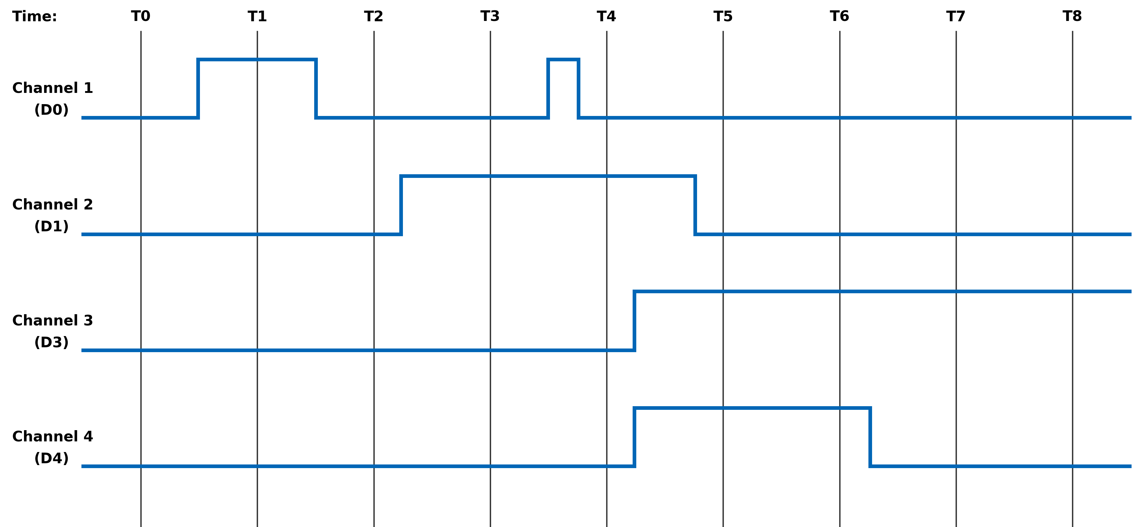
Dynamic and Latched Status Registers Examples
The examples in this section illustrate the differences in behavior of the Dynamic Status and Latched Status registers as well as the differences in behavior of Edge/Level Trigger when the Latched Status register is cleared.
Figure 1. Example of Module's Channel-Mapped Dynamic and Latched Status States
No Clearing of
Latched StatusClearing of Latched Status
(Edge-Triggered)Clearing of Latched Status
(Level-Triggered)Time Dynamic Status Latched Status Action Latched Status Action Latched T0 0x0 0x0 Read Latched Register 0x0 Read Latched Register 0x0 T1 0x1 0x1 Read Latched Register 0x1 0x1 T1 0x1 0x1 Write 0x1 to Latched Register Write 0x1 to Latched Register T1 0x1 0x1 0x0 0x1 T2 0x0 0x1 Read Latched Register 0x0 Read Latched Register 0x1 T2 0x0 0x1 Read Latched Register 0x0 Write 0x1 to Latched Register T2 0x0 0x1 Read Latched Register 0x0 0x0 T3 0x2 0x3 Read Latched Register 0x2 Read Latched Register 0x2 T3 0x2 0x3 Write 0x2 to Latched Register Write 0x2 to Latched Register T3 0x2 0x3 0x0 0x2 T4 0x2 0x3 Read Latched Register 0x1 Read Latched Register 0x3 T4 0x2 0x3 Write 0x1 to Latched Register Write 0x3 to Latched Register T4 0x2 0x3 0x0 0x2 T5 0xC 0xF Read Latched Register 0xC Read Latched Register 0xE T5 0xC 0xF Write 0xC to Latched Register Write 0xE to Latched Register T5 0xC 0xF 0x0 0xC T6 0xC 0xF Read Latched Register 0x0 Read Latched 0xC T6 0xC 0xF Read Latched Register 0x0 Write 0xC to Latched Register T6 0xC 0xF Read Latched Register 0x0 0xC T7 0x4 0xF Read Latched Register 0x0 Read Latched Register 0xC T7 0x4 0xF Read Latched Register 0x0 Write 0xC to Latched Register T7 0x4 0xF Read Latched Register 0x0 0x4 T8 0x4 0xF Read Latched Register 0x0 Read Latched Register 0x4 Interrupt Examples
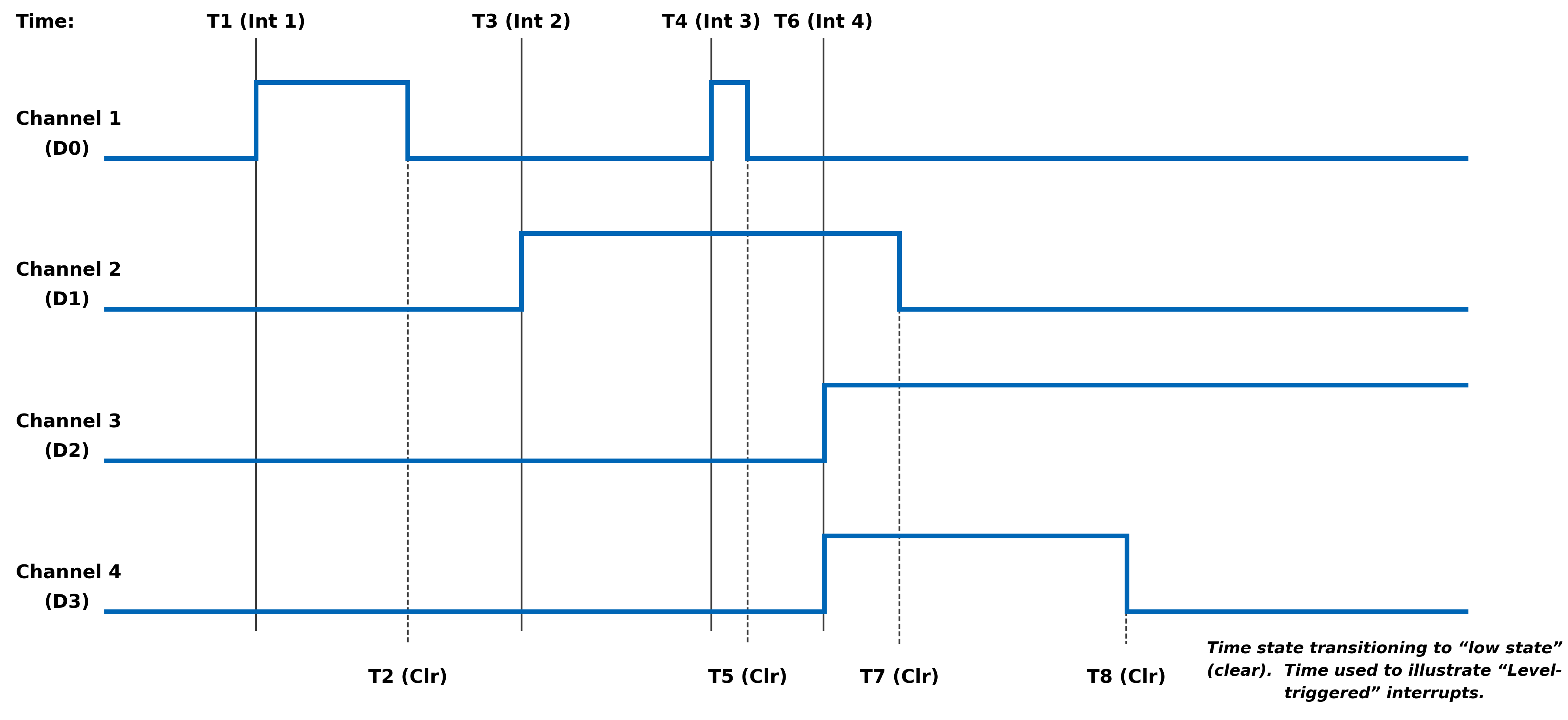
The examples in this section illustrate the interrupt behavior with Edge/Level Trigger.
Figure 2. Illustration of Latched Status State for Module with 4-Channels with Interrupt Enabled
Time Latched Status
(Edge-Triggered -
Clear Multi-Channel)Latched Status
(Edge-Triggered -
Clear Single Channel)Latched Status
(Level-Triggered -
Clear Multi-Channel)Action Latched Action Latched Action Latched T1
(Int 1)Interrupt Generated
Read Latched Registers0x1 Interrupt Generated
Read Latched Registers0x1 Interrupt Generated
Read Latched Registers0x1 T1
(Int 1)Write 0x1 to Latched Register Write 0x1 to Latched Register Write 0x1 to Latched Register T1
(Int 1)0x0 0x0 Interrupt re-triggers
Note, interrupt re-triggers after
each clear until T2.0x1 T3
(Int 2)Interrupt Generated
Read Latched Registers0x2 Interrupt Generated
Read Latched Registers0x2 Interrupt Generated
Read Latched Registers0x2 T3
(Int 2)Write 0x2 to Latched Register Write 0x2 to Latched Register Write 0x2 to Latched Register T3
(Int 2)0x0 0x0 Interrupt re-triggers
Note, interrupt re-triggers after
each clear until T7.0x2 T4
(Int 3)Interrupt Generated
Read Latched Registers0x1 Interrupt Generated
Read Latched Registers0x1 Interrupt Generated
Read Latched Registers0x3 T4
(Int 3)Write 0x1 to Latched Register Write 0x1 to Latched Register Write 0x3 to Latched Register T4
(Int 3)0x0 0x0 Interrupt re-triggers
Note, interrupt re-triggers after
each clear and 0x3 is reported
in Latched Register until T5.0x3 T4
(Int 3)0x0 0x0 Interrupt re-triggers
Note, interrupt re-triggers after
each clear until T7.0x2 T6
(Int 4)Interrupt Generated
Read Latched Registers0xC Interrupt Generated
Read Latched Registers0xC Interrupt Generated
Read Latched Registers0xE T6
(Int 4)Write 0xC to Latched Register Write 0x4 to Latched Register Write 0xE to Latched Register T6
(Int 4)0x0 Interrupt re-triggers
Write 0x8 to Latched Register0x8 Interrupt re-triggers
Note, interrupt re-triggers after
each clear and 0xE is
reported in Latched Register until T7.0xE T6
(Int 4)0x0 0x0 Interrupt re-triggers
Note, interrupt re-triggers after
each clear and 0xC is
reported in Latched Register until T8.0xC T6
(Int 4)0x0 0x0 Interrupt re-triggers
Note, interrupt re-triggers after
each clear and 0x4 is
reported in Latched Register always.0x4 REVISION HISTORY
Motherboard Manual - Status and Interrupts Revision History Revision Revision Date Description C 2021-11-30 C08896; Transition manual to docbuilder format - no technical info change. Link to original
DOCS.NAII REVISIONS Revision Date Description 2026-03-02 Formatting updates to document; no technical changes. 2026-05-18 Fixed formatting issues from conversion to new doc site format. 2026-05-19 Fixed minor formatting issue with Interrupt Examples table structure (removed extraneous cell). 2026-07-15 Revised image files for image quality.
MODULE COMMON REGISTERS
The registers described in this document are common to all NAI Generation 5 modules.
Module Information Registers
The registers in this section provide module information such as firmware revisions, capabilities and unique serial number information.
FPGA Version Registers
The FPGA firmware version registers include registers that contain the Revision, Compile Timestamp, SerDes Revision, Template Revision and Zynq Block Revision information.
FPGA Revision Function: FPGA firmware revision Type: unsigned binary word (32-bit) Data Range: 0x0000 0000 to 0xFFFF FFFF Read/Write: R Initialized Value: Value corresponding to the revision of the board's FPGA Operational Settings: The upper 16-bits are the major revision and the lower 16-bits are the minor revision.
D31 D30 D29 D28 D27 D26 D25 D24 D23 D22 D21 D20 D19 D18 D17 D16 Major Revision Number D15 D14 D13 D12 D11 D10 D9 D8 D7 D6 D5 D4 D3 D2 D1 D0 Minor Revision Number
FPGA Compile Timestamp Function: Compile Timestamp for the FPGA firmware. Type: unsigned binary word (32-bit) Data Range: N/A Read/Write: R Initialized Value: Value corresponding to the compile timestamp of the board's FPGA Operational Settings: The 32-bit value represents the Day, Month, Year, Hour, Minutes and Seconds as formatted in the table:
D31 D30 D29 D28 D27 D26 D25 D24 D23 D22 D21 D20 D19 D18 D17 D16 day (5-bits) month (4-bits) year (6-bits) hr D15 D14 D13 D12 D11 D10 D9 D8 D7 D6 D5 D4 D3 D2 D1 D0 hour (5-bits) minutes (6-bits) seconds (6-bits)
FPGA SerDes Revision Function: FPGA SerDes revision Type: unsigned binary word (32-bit) Data Range: 0x0000 0000 to 0xFFFF FFFF Read/Write: R Initialized Value: Value corresponding to the SerDes revision of the board's FPGA Operational Settings: The upper 16-bits are the major revision, and the lower 16-bits are the minor revision.
D31 D30 D29 D28 D27 D26 D25 D24 D23 D22 D21 D20 D19 D18 D17 D16 Major Revision Number D15 D14 D13 D12 D11 D10 D9 D8 D7 D6 D5 D4 D3 D2 D1 D0 Minor Revision Number
FPGA Template Revision Function: FPGA Template revision Type: unsigned binary word (32-bit) Data Range: 0x0000 0000 to 0xFFFF FFFF Read/Write: R Initialized Value: Value corresponding to the template revision of the board's FPGA Operational Settings: The upper 16-bits are the major revision, and the lower 16-bits are the minor revision.
D31 D30 D29 D28 D27 D26 D25 D24 D23 D22 D21 D20 D19 D18 D17 D16 Major Revision Number D15 D14 D13 D12 D11 D10 D9 D8 D7 D6 D5 D4 D3 D2 D1 D0 Minor Revision Number
FPGA Zynq Block Revision Function: FPGA Zynq Block revision Type: unsigned binary word (32-bit) Data Range: 0x0000 0000 to 0xFFFF FFFF Read/Write: R Initialized Value: Value corresponding to the Zynq block revision of the board's FPGA Operational Settings: The upper 16-bits are the major revision, and the lower 16-bits are the minor revision.
D31 D30 D29 D28 D27 D26 D25 D24 D23 D22 D21 D20 D19 D18 D17 D16 Major Revision Number D15 D14 D13 D12 D11 D10 D9 D8 D7 D6 D5 D4 D3 D2 D1 D0 Minor Revision Number Bare Metal Version Registers
The Bare Metal firmware version registers include registers that contain the Revision and Compile Time information.
Bare Metal Revision Function: Bare Metal firmware revision Type: unsigned binary word (32-bit) Data Range: 0x0000 0000 to 0xFFFF FFFF Read/Write: R Initialized Value: Value corresponding to the revision of the board's Bare Metal Operational Settings: The upper 16-bits are the major revision and the lower 16-bits are the minor revision.
D31 D30 D29 D28 D27 D26 D25 D24 D23 D22 D21 D20 D19 D18 D17 D16 Major Revision Number D15 D14 D13 D12 D11 D10 D9 D8 D7 D6 D5 D4 D3 D2 D1 D0 Minor Revision Number
Bare Metal Compile Time Function: Provides an ASCII representation of the Date/Time for the Bare Metal compile time. Type: 24-character ASCII string - Six (6) unsigned binary word (32-bit) Data Range: N/A Read/Write: R Initialized Value: Value corresponding to the ASCII representation of the compile time of the board's Bare Metal Operational Settings: The six 32-bit words provide an ASCII representation of the Date/Time. The hexadecimal values in the field below represent: May 17 2019 at 15:38:32 Note
little-endian order of ASCII values
Word 1 (Ex. 0x2079614D) D31 D30 D29 D28 D27 D26 D25 D24 D23 D22 D21 D20 D19 D18 D17 D16 Space (0x20) Month ('y' - 0x79) D15 D14 D13 D12 D11 D10 D9 D8 D7 D6 D5 D4 D3 D2 D1 D0 Month ('a' - 0x61) Month ('M' - 0x4D) Word 2 (Ex. 0x32203731) D31 D30 D29 D28 D27 D26 D25 D24 D23 D22 D21 D20 D19 D18 D17 D16 Year ('2' - 0x32) Space (0x20) D15 D14 D13 D12 D11 D10 D9 D8 D7 D6 D5 D4 D3 D2 D1 D0 Day ('7' - 0x37) Day ('1' - 0x31) Word 3 (Ex. 0x20393130) D31 D30 D29 D28 D27 D26 D25 D24 D23 D22 D21 D20 D19 D18 D17 D16 Space (0x20) Year ('9' - 0x39) D15 D14 D13 D12 D11 D10 D9 D8 D7 D6 D5 D4 D3 D2 D1 D0 Year ('1' - 0x31) Year ('0' - 0x30) Word 4 (Ex. 0x31207461) D31 D30 D29 D28 D27 D26 D25 D24 D23 D22 D21 D20 D19 D18 D17 D16 Hour ('1' - 0x31) Space (0x20) D15 D14 D13 D12 D11 D10 D9 D8 D7 D6 D5 D4 D3 D2 D1 D0 'a' (0x74) 't' (0x61) Word 5 (Ex. 0x38333A35) D31 D30 D29 D28 D27 D26 D25 D24 D23 D22 D21 D20 D19 D18 D17 D16 Minute ('8' - 0x38) Minute ('3' - 0x33) D15 D14 D13 D12 D11 D10 D9 D8 D7 D6 D5 D4 D3 D2 D1 D0 ':' (0x3A) Hour ('5' - 0x35) Word 6 (Ex. 0x0032333A) D31 D30 D29 D28 D27 D26 D25 D24 D23 D22 D21 D20 D19 D18 D17 D16 NULL (0x00) Seconds ('2' - 0x32) D15 D14 D13 D12 D11 D10 D9 D8 D7 D6 D5 D4 D3 D2 D1 D0 Seconds ('3' - 0x33) ':' (0x3A) FSBL Version Registers
The FSBL version registers include registers that contain the Revision and Compile Time information for the First Stage Boot Loader (FSBL).
FSBL Revision Function: FSBL firmware revision Type: unsigned binary word (32-bit) Data Range: 0x0000 0000 to 0xFFFF FFFF Read/Write: R Initialized Value: Value corresponding to the revision of the board's FSBL Operational Settings: The upper 16-bits are the major revision, and the lower 16-bits are the minor revision.
D31 D30 D29 D28 D27 D26 D25 D24 D23 D22 D21 D20 D19 D18 D17 D16 Major Revision Number D15 D14 D13 D12 D11 D10 D9 D8 D7 D6 D5 D4 D3 D2 D1 D0 Minor Revision Number
FSBL Compile Time Function: Provides an ASCII representation of the Date/Time for the FSBL compile time. Type: 24-character ASCII string - Six (6) unsigned binary word (32-bit) Data Range: N/A Read/Write: R Initialized Value: Value corresponding to the ASCII representation of the Compile Time of the board's FSBL Operational Settings: The six 32-bit words provide an ASCII representation of the Date/Time. The hexadecimal values in the field below represent: May 17 2019 at 15:38:32
Note
little-endian order of ASCII values
Word 1 (Ex. 0x2079614D) D31 D30 D29 D28 D27 D26 D25 D24 D23 D22 D21 D20 D19 D18 D17 D16 Space (0x20) Month ('y' - 0x79) D15 D14 D13 D12 D11 D10 D9 D8 D7 D6 D5 D4 D3 D2 D1 D0 Month ('a' - 0x61) Month ('M' - 0x4D) Word 2 (Ex. 0x32203731) D31 D30 D29 D28 D27 D26 D25 D24 D23 D22 D21 D20 D19 D18 D17 D16 Year ('2' - 0x32) Space (0x20) D15 D14 D13 D12 D11 D10 D9 D8 D7 D6 D5 D4 D3 D2 D1 D0 Day ('7' - 0x37) Day ('1' - 0x31) Word 3 (Ex. 0x20393130) D31 D30 D29 D28 D27 D26 D25 D24 D23 D22 D21 D20 D19 D18 D17 D16 Space (0x20) Year ('9' - 0x39) D15 D14 D13 D12 D11 D10 D9 D8 D7 D6 D5 D4 D3 D2 D1 D0 Year ('1' - 0x31) Year ('0' - 0x30) Word 4 (Ex. 0x31207461) D31 D30 D29 D28 D27 D26 D25 D24 D23 D22 D21 D20 D19 D18 D17 D16 Hour ('1' - 0x31) Space (0x20) D15 D14 D13 D12 D11 D10 D9 D8 D7 D6 D5 D4 D3 D2 D1 D0 'a' (0x74) 't' (0x61) Word 5 (Ex. 0x38333A35) D31 D30 D29 D28 D27 D26 D25 D24 D23 D22 D21 D20 D19 D18 D17 D16 Minute ('8' - 0x38) Minute ('3' - 0x33) D15 D14 D13 D12 D11 D10 D9 D8 D7 D6 D5 D4 D3 D2 D1 D0 ':' (0x3A) Hour ('5' - 0x35) Word 6 (Ex. 0x0032333A) D31 D30 D29 D28 D27 D26 D25 D24 D23 D22 D21 D20 D19 D18 D17 D16 NULL (0x00) Seconds ('2' - 0x32) D15 D14 D13 D12 D11 D10 D9 D8 D7 D6 D5 D4 D3 D2 D1 D0 Seconds ('3' - 0x33) ':' (0x3A) Module Serial Number Registers
The Module Serial Number registers include registers that contain the Serial Numbers for the Interface Board and the Functional Board of the module.
Interface Board Serial Number Function: Unique 128-bit identifier used to identify the interface board. Type: 16-character ASCII string - Four (4) unsigned binary words (32-bit) Data Range: N/A Read/Write: R Initialized Value: Serial number of the interface board Operational Settings: This register is for information purposes only.
Functional Board Serial Number Function: Unique 128-bit identifier used to identify the functional board. Type: 16-character ASCII string - Four (4) unsigned binary words (32-bit) Data Range: N/A Read/Write: R Initialized Value: Serial number of the functional board Operational Settings: This register is for information purposes only.
Module Capability Function: Provides indication for whether or not the module can support the following: SerDes block reads, SerDes FIFO block reads, SerDes packing (combining two 16-bit values into one 32-bit value) and floating point representation. The purpose for block access and packing is to improve the performance of accessing larger amounts of data over the SerDes interface. Type: unsigned binary word (32-bit) Data Range: 0x0000 0000 to 0x0000 0107 Read/Write: R Initialized Value: 0x0000 0107 Operational Settings: A “1” in the bit associated with the capability indicates that it is supported.
D31 D30 D29 D28 D27 D26 D25 D24 D23 D22 D21 D20 D19 D18 D17 D16 0 0 0 0 0 0 0 0 0 0 0 0 0 0 0 0 D15 D14 D13 D12 D11 D10 D9 D8 D7 D6 D5 D4 D3 D2 D1 D0 0 0 0 0 0 0 0 Flt-Pt 0 0 0 0 0 Pack FIFO Blk Blk
Module Memory Map Revision Function: Module Memory Map revision Type: unsigned binary word (32-bit) Data Range: 0x0000 0000 to 0xFFFF FFFF Read/Write: R Initialized Value: Value corresponding to the Module Memory Map Revision Operational Settings: The upper 16-bits are the major revision and the lower 16-bits are the minor revision.
D31 D30 D29 D28 D27 D26 D25 D24 D23 D22 D21 D20 D19 D18 D17 D16 Major Revision Number D15 D14 D13 D12 D11 D10 D9 D8 D7 D6 D5 D4 D3 D2 D1 D0 Minor Revision Number Module Measurement Registers
The registers in this section provide module temperature measurement information.
Temperature Readings Registers
The temperature registers provide the current, maximum (from power-up) and minimum (from power-up) Zynq and PCB temperatures.
Interface Board Current Temperature Function: Measured PCB and Zynq Core temperatures on Interface Board. Type: signed byte (8-bits) for PCB and signed byte (8-bits) for Zynq core temperatures Data Range: 0x0000 0000 to 0x0000 FFFF Read/Write: R Initialized Value: Value corresponding to the measured PCB and Zynq core temperatures based on the table below Operational Settings: The upper 16-bits are not used, and the lower 16-bits are the PCB and Zynq Core Temperatures. For example, if the register contains the value 0x0000 202C, this represents PCB Temperature = 32° Celsius and Zynq Temperature = 44° Celsius.
D31 D30 D29 D28 D27 D26 D25 D24 D23 D22 D21 D20 D19 D18 D17 D16 0 0 0 0 0 0 0 0 0 0 0 0 0 0 0 0 D15 D14 D13 D12 D11 D10 D9 D8 D7 D6 D5 D4 D3 D2 D1 D0 PCB Temperature Zynq Core Temperature
Functional Board Current Temperature Function: Measured PCB temperature on Functional Board. Type: signed byte (8-bits) for PCB Data Range: 0x0000 0000 to 0x0000 00FF Read/Write: R Initialized Value: Value corresponding to the measured PCB on the table below Operational Settings: The upper 24-bits are not used, and the lower 8-bits are the PCB Temperature. For example, if the register contains the value 0x0000 0019, this represents PCB Temperature = 25° Celsius.
D31 D30 D29 D28 D27 D26 D25 D24 D23 D22 D21 D20 D19 D18 D17 D16 0 0 0 0 0 0 0 0 0 0 0 0 0 0 0 0 D15 D14 D13 D12 D11 D10 D9 D8 D7 D6 D5 D4 D3 D2 D1 D0 0 0 0 0 0 0 0 0 PCB Temperature
Interface Board Maximum Temperature Function: Maximum PCB and Zynq Core temperatures on Interface Board since power-on. Type: signed byte (8-bits) for PCB and signed byte (8-bits) for Zynq core temperatures Data Range: 0x0000 0000 to 0x0000 FFFF Read/Write: R Initialized Value: Value corresponding to the maximum measured PCB and Zynq core temperatures since power-on based on the table below Operational Settings: The upper 16-bits are not used, and the lower 16-bits are the maximum PCB and Zynq Core Temperatures. For example, if the register contains the value 0x0000 5569, this represents maximum PCB Temperature = 85° Celsius and maximum Zynq Temperature = 105° Celsius.
D31 D30 D29 D28 D27 D26 D25 D24 D23 D22 D21 D20 D19 D18 D17 D16 0 0 0 0 0 0 0 0 0 0 0 0 0 0 0 0 D15 D14 D13 D12 D11 D10 D9 D8 D7 D6 D5 D4 D3 D2 D1 D0 PCB Temperature Zynq Core Temperature
Interface Board Minimum Temperature Function: Minimum PCB and Zynq Core temperatures on Interface Board since power-on. Type: signed byte (8-bits) for PCB and signed byte (8-bits) for Zynq core temperatures Data Range: 0x0000 0000 to 0x0000 FFFF Read/Write: R Initialized Value: Value corresponding to the minimum measured PCB and Zynq core temperatures since power-on based on the table below Operational Settings: The upper 16-bits are not used, and the lower 16-bits are the minimum PCB and Zynq Core Temperatures. For example, if the register contains the value 0x0000 D8E7, this represents minimum PCB Temperature = -40° Celsius and minimum Zynq Temperature = -25° Celsius.
D31 D30 D29 D28 D27 D26 D25 D24 D23 D22 D21 D20 D19 D18 D17 D16 0 0 0 0 0 0 0 0 0 0 0 0 0 0 0 0 D15 D14 D13 D12 D11 D10 D9 D8 D7 D6 D5 D4 D3 D2 D1 D0 PCB Temperature Zynq Core Temperature
Functional Board Maximum Temperature Function: Maximum PCB temperature on Functional Board since power-on. Type: signed byte (8-bits) for PCB Data Range: 0x0000 0000 to 0x0000 00FF Read/Write: R Initialized Value: Value corresponding to the measured PCB on the table below Operational Settings: The upper 24-bits are not used, and the lower 8-bits are the PCB Temperature. For example, if the register contains the value 0x0000 0055, this represents PCB Temperature = 85° Celsius.
D31 D30 D29 D28 D27 D26 D25 D24 D23 D22 D21 D20 D19 D18 D17 D16 0 0 0 0 0 0 0 0 0 0 0 0 0 0 0 0 D15 D14 D13 D12 D11 D10 D9 D8 D7 D6 D5 D4 D3 D2 D1 D0 0 0 0 0 0 0 0 0 PCB Temperature
Functional Board Minimum Temperature Function: Minimum PCB temperature on Functional Board since power-on. Type: signed byte (8-bits) for PCB Data Range: 0x0000 0000 to 0x0000 00FF Read/Write: R Initialized Value: Value corresponding to the measured PCB on the table below Operational Settings: The upper 24-bits are not used, and the lower 8-bits are the PCB Temperature. For example, if the register contains the value 0x0000 00D8, this represents PCB Temperature = -40° Celsius.
D31 D30 D29 D28 D27 D26 D25 D24 D23 D22 D21 D20 D19 D18 D17 D16 0 0 0 0 0 0 0 0 0 0 0 0 0 0 0 0 D15 D14 D13 D12 D11 D10 D9 D8 D7 D6 D5 D4 D3 D2 D1 D0 0 0 0 0 0 0 0 0 PCB Temperature Higher Precision Temperature Readings Registers
These registers provide higher precision readings of the current Zynq and PCB temperatures.
Higher Precision Zynq Core Temperature Function: Higher precision measured Zynq Core temperature on Interface Board. Type: signed word (16-bits) for integer part and unsigned word (16-bits) for fractional part Data Range: 0x0000 0000 to 0xFFFF FFFF Read/Write: R Initialized Value: Measured Zynq Core temperature on Interface Board Operational Settings: The upper 16-bits represent the signed integer part of the temperature and the lower 16-bits represent the fractional part of the temperature with the resolution of 1/1000 of degree Celsius. For example, if the register contains the value 0x002B 0271, this represents Zynq Core Temperature = 43.625° Celsius, and value 0xFFF6 0177 represents -10.375° Celsius.
D31 D30 D29 D28 D27 D26 D25 D24 D23 D22 D21 D20 D19 D18 D17 D16 Signed Integer Part of Temperature D15 D14 D13 D12 D11 D10 D9 D8 D7 D6 D5 D4 D3 D2 D1 D0 Fractional Part of Temperature
Higher Precision Interface PCB Temperature Function: Higher precision measured Interface PCB temperature. Type: signed word (16-bits) for integer part and unsigned word (16-bits) for fractional part Data Range: 0x0000 0000 to 0xFFFF FFFF Read/Write: R Initialized Value: Measured Interface PCB temperature Operational Settings: The upper 16-bits represent the signed integer part of the temperature and the lower 16-bits represent the fractional part of the temperature with the resolution of 1/1000 of degree Celsius. For example, if the register contains the value 0x0020 007D, this represents Interface PCB Temperature = 32.125° Celsius, and value 0xFFE8 036B represents -24.875° Celsius.
D31 D30 D29 D28 D27 D26 D25 D24 D23 D22 D21 D20 D19 D18 D17 D16 Signed Integer Part of Temperature D15 D14 D13 D12 D11 D10 D9 D8 D7 D6 D5 D4 D3 D2 D1 D0 Fractional Part of Temperature
Higher Precision Functional PCB Temperature Function: Higher precision measured Functional PCB temperature. Type: signed word (16-bits) for integer part and unsigned word (16-bits) for fractional part Data Range: 0x0000 0000 to 0xFFFF FFFF Read/Write: R Initialized Value: Measured Functional PCB temperature Operational Settings: The upper 16-bits represent the signed integer part of the temperature and the lower 16-bits represent the fractional part of the temperature with the resolution of 1/100 of degree Celsius. For example, if the register contains the value 0x0018 004B, this represents Functional PCB Temperature = 24.75° Celsius, and value 0xFFD9 0019 represents -39.25° Celsius.
D31 D30 D29 D28 D27 D26 D25 D24 D23 D22 D21 D20 D19 D18 D17 D16 Signed Integer Part of Temperature D15 D14 D13 D12 D11 D10 D9 D8 D7 D6 D5 D4 D3 D2 D1 D0 Fractional Part of Temperature Module Health Monitoring Registers
The registers in this section provide module temperature measurement information. If the temperature measurements reaches the Lower Critical or Upper Critical conditions, the module will automatically reset itself to prevent damage to the hardware.
Module Sensor Summary Status Function: The corresponding sensor bit is set if the sensor has crossed any of its thresholds. Type: unsigned binary word (32-bits) Data Range: See table below Read/Write: R Initialized Value: 0 Operational Settings: This register provides a summary for module sensors. When the corresponding sensor bit is set, the Sensor Threshold Status register for that sensor will indicate the threshold condition that triggered the event.
Bit(s) Sensor D31:D6 Reserved D5 Functional Board PCB Temperature D4 Interface Board PCB Temperature D3:D0 Reserved Module Sensor Registers
The registers listed in this section apply to each module sensor listed for the Module Sensor Summary Status register. Each individual sensor register provides a group of registers for monitoring module temperatures readings. From these registers, a user can read the current temperature of the sensor in addition to the minimum and maximum temperature readings since power-up. Upper and lower critical/warning temperature thresholds can be set and monitored from these registers. When a programmed temperature threshold is crossed, the Sensor Threshold Status register will set the corresponding bit for that threshold. The figure below shows the functionality of this group of registers when accessing the Interface Board PCB Temperature sensor as an example.
Sensor Threshold Status Function: Reflects which threshold has been crossed Type: unsigned binary word (32-bits) Data Range: See table below Read/Write: R Initialized Value: 0 Operational Settings: The associated bit is set when the sensor reading exceed the corresponding threshold settings.
Bit(s) Description D31:D4 Reserved D3 Exceeded Upper Critical Threshold D2 Exceeded Upper Warning Threshold D1 Exceeded Lower Critical Threshold D0 Exceeded Lower Warning Threshold
Sensor Current Reading Function: Reflects current reading of temperature sensor Type: Single Precision Floating Point Value (IEEE-754) Data Range: Single Precision Floating Point Value (IEEE-754) Read/Write: R Initialized Value: N/A Operational Settings: The register represents current sensor reading as a single precision floating point value. For example, for a temperature sensor, register value 0x41C6 0000 represents temperature = 24.75° Celsius.
Sensor Minimum Reading Function: Reflects minimum value of temperature sensor since power up Type: Single Precision Floating Point Value (IEEE-754) Data Range: Single Precision Floating Point Value (IEEE-754) Read/Write: R Initialized Value: N/A Operational Settings: The register represents minimum sensor value as a single precision floating point value. For example, for a temperature sensor, register value 0x41C6 0000 represents temperature = 24.75° Celsius.
Sensor Maximum Reading Function: Reflects maximum value of temperature sensor since power up Type: Single Precision Floating Point Value (IEEE-754) Data Range: Single Precision Floating Point Value (IEEE-754) Read/Write: R Initialized Value: N/A Operational Settings: The register represents maximum sensor value as a single precision floating point value. For example, for a temperature sensor, register value 0x41C6 0000 represents temperature = 24.75° Celsius.
Sensor Lower Warning Threshold Function: Reflects lower warning threshold of temperature sensor Type: Single Precision Floating Point Value (IEEE-754) Data Range: Single Precision Floating Point Value (IEEE-754) Read/Write: R/W Initialized Value: Default lower warning threshold (value dependent on specific sensor) Operational Settings: The register represents sensor lower warning threshold as a single precision floating point value. For example, for a temperature sensor, register value 0xC220 0000 represents temperature = -40.0° Celsius.
Sensor Lower Critical Threshold Function: Reflects lower critical threshold of temperature sensor Type: Single Precision Floating Point Value (IEEE-754) Data Range: Single Precision Floating Point Value (IEEE-754) Read/Write: R/W Initialized Value: Default lower critical threshold (value dependent on specific sensor) Operational Settings: The register represents sensor lower critical threshold as a single precision floating point value. For example, for a temperature sensor, register value 0xC25C 0000 represents temperature = -55.0° Celsius.
Sensor Upper Warning Threshold Function: Reflects upper warning threshold of temperature sensor Type: Single Precision Floating Point Value (IEEE-754) Data Range: Single Precision Floating Point Value (IEEE-754) Read/Write: R/W Initialized Value: Default upper warning threshold (value dependent on specific sensor) Operational Settings: The register represents sensor upper warning threshold as a single precision floating point value. For example, for a temperature sensor, register value 0x42AA 0000 represents temperature = 85.0° Celsius.
Sensor Upper Critical Threshold Function: Reflects upper critical threshold of temperature sensor Type: Single Precision Floating Point Value (IEEE-754) Data Range: Single Precision Floating Point Value (IEEE-754) Read/Write: R/W Initialized Value: Default upper critical threshold (value dependent on specific sensor) Operational Settings: The register represents sensor upper critical threshold as a single precision floating point value. For example, for a temperature sensor, register value 0x42FA 0000 represents temperature = 125.0° Celsius. FUNCTION REGISTER MAP
KEY
Configuration/Control Measurement/Status/Board Information
MODULE INFORMATION REGISTERS OFFSET REGISTER NAME ACCESS OFFSET REGISTER NAME ACCESS 0x003C FPGA Revision R 0x0074 Bare Metal Revision R 0x0030 FPGA Compile Timestamp R 0x0080 Bare Metal Compile Time (Bit 0-31) R 0x0034 FPGA SerDes Revision R 0x0084 Bare Metal Compile Time (Bit 32-63) R 0x0038 FPGA Template Revision R 0x0088 Bare Metal Compile Time (Bit 64-95) R 0x0040 FPGA Zynq Block Revision R 0x008C Bare Metal Compile Time (Bit 96-127) R 0x0090 Bare Metal Compile Time (Bit 128-159) R 0x0094 Bare Metal Compile Time (Bit 160-191) R 0x007C FSBL Revision R 0x00B0 FSBL Compile Time (Bit 0-31) R 0x00B4 FSBL Compile Time (Bit 32-63) R 0x00B8 FSBL Compile Time (Bit 64-95) R 0x00BC FSBL Compile Time (Bit 96-127) R 0x00C0 FSBL Compile Time (Bit 128-159) R 0x00C4 FSBL Compile Time (Bit 160-191) R 0x0000 Interface Board Serial Number (Bit 0-31) R 0x0010 Functional Board Serial Number (Bit 0-31) R 0x0034 Interface Board Serial Number (Bit 32-63) R 0x0014 Functional Board Serial Number (Bit 32-63) R 0x0008 Interface Board Serial Number (Bit 64-95) R 0x0018 Functional Board Serial Number (Bit 64-95) R 0x000C Interface Board Serial Number (Bit 96-127) R 0x001C Functional Board Serial Number (Bit 96-127) R 0x0070 Module Capability R 0x01FC Module Memory Map Revision R
MODULE MEASUREMENTS REGISTERS OFFSET REGISTER NAME ACCESS OFFSET REGISTER NAME ACCESS 0x0200 Interface Board PCB/Zynq Current Temp R 0x0208 Functional Board PCB Current Temp R 0x0218 Interface Board PCB/Zynq Max Temp R 0x0228 Functional Board PCB Max Temp R 0x0220 Interface Board PCB/Zynq Min Temp R 0x0230 Functional Board PCB Min Temp R 0x02C0 Higher Precision Zynq Core Temperature R 0x02C4 Higher Precision Interface PCB Temperature R 0x02E0 Higher Precision Functional PCB Temperature R
MODULE HEALTH MONITORING REGISTERS OFFSET REGISTER NAME ACCESS OFFSET REGISTER NAME ACCESS 0x07F8 Module Sensor Summary Status R
REVISION HISTORY
Motherboard Manual - Module Common Registers Revision History Revision Revision Date Description C 2023-08-11 ECO C10649, initial release of module common registers manual. C1 2024-05-15 ECO C11522, removed Zynq Core/Aux/DDR Voltage register descriptions from Module Measurement Registers. Pg.16, updated Module Sensor Summary Status register to add PS references; updated Bit Table to change voltage/current bits to 'reserved'. Pg.16, updated Module/Power Supply Sensor Registers description to better describe register functionality and to add figure. Pg.17, added 'Exceeded' to threshold bit descriptions. Pg.17-18, removed voltage/current references from sensor descriptions. Pg.20, removed Zynq Core/Aux/DDR Voltage register offsets from Module Measurement Registers. Pg.20, updated Module Health Monitoring Registers offset tables. C2 2024-07-10 ECO C11701, pg.16, updated Module Sensor Summary Status register to remove PS references;updated Bit Table to change PS temperature bits to 'reserved'. Pg.16, updated Module SensorRegisters description to remove PS references. Pg.20, updated Module Health MonitoringRegisters offset tables to remove PS temperature register offsets. Link to original
DOCS.NAII REVISIONS Revision Date Description 2025-11-05 Corrected register offsets for Interface Board Min Temp and Function Board Min & Max Temps. 2026-03-02 Formatting updates to document; no technical changes. 2026-05-20 Minor formatting fixes (non-technical changes). 2026-07-15 Updated images for online quality; minor additional formatting updates (no technical changes).


Revision History
Module Manual - RG1 Revision History
| Revision | Revision | Date Description |
|---|---|---|
| C | 2022-09-16 | ECO C09625, initial release of module manual. |
| C1 | 2024-01-04 | ECO C11122, pg.5, removed reference to independent input/output. Pg.8, removed reference to independent input/output from Principle of Operation. Pg.9/29/34, added Module Common Registers. Pg.36, defined pin DATIO20 as ISO_GND and added accompanying note. |
Module Manual - Status and Interrupts Revision History
| Revision | Revision Date | Description |
|---|---|---|
| C | 2021-11-30 | C08896; Transition manual to docbuilder format - no technical info change. |
Module Manual - Module Common Registers Revision History
| Revision | Revision Date | Description |
|---|---|---|
| C | 2023-08-11 | ECO C10649, initial release of module common registers manual. |
NAI Cares
North Atlantic Industries (NAI) is a leading independent supplier of Embedded I/O Boards, Single Board Computers, Rugged Power Supplies, Embedded Systems and Motion Simulation and Measurement Instruments for the Military, Aerospace and Industrial Industries. We accelerate our clients’ time-to-mission with a unique approach based on a Configurable Open Systems Architecture™ (COSA®) that delivers the best of both worlds: custom solutions from standard COTS components.
We have built a reputation by listening to our customers, understanding their needs, and designing, testing and delivering board and system-level products for their most demanding air, land and sea requirements. If you have any applications or questions regarding the use of our products, please contact us for an expedient solution.
Please visit us at: www.naii.com or select one of the following for immediate assistance:
Documentation
FAQ
Application Notes
http://www.naii.com/applicationnotes
Calibration and Repairs
http://www.naii.com/calibrationrepairs
Call Us
(631) 567-1100
Link to original