CME, CMF
Analog-to-Digital & Digital-to-Analog Combination Function Module
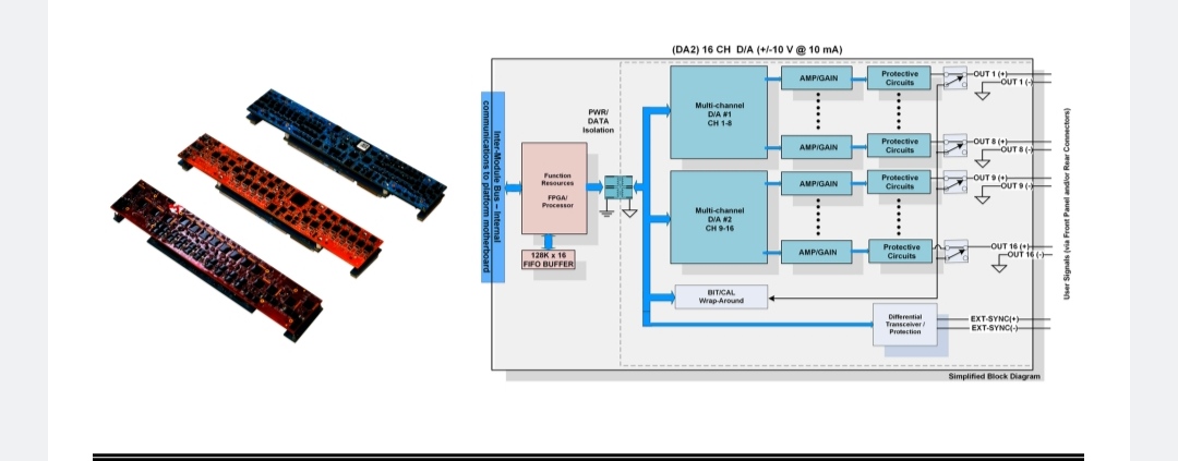
CME-CMF Combination Modules Analog-to-Digital Function Modules Combination Module: 8-Ch. A/D (CME = ±10 V, CMF = ±100 V) and 8-Ch. D/A (±10.0 V @ 10 mA)
The CME/CMF smart function modules provide a combined function alternative which mitigates SWaP-C (Size, Weight, Power, & Cost) system integration and configuration challenges. The CME/CMF functions essentially combine two of NAI’s popular functions onto a single-slot function module:
Analog-to-Digital (A/D) I/O Interface : The CME/CMF smart functions provide an Analog-to-Digital (A/D) I/O Interface (like the ADE/ADF smart function modules) with eight (8) independent 16-bit Successive Approximation Register (SAR) A/D input channels which support a maximum input voltage range of ±10 V (for CME) or ±100 V (for CMF).
Digital-to-Analog (D/A) I/O Interface: The CME/CMF smart functions provide a Digital-to-Analog (D/A) I/O Interface (like the DA2 smart function module) with eight (8) independent 16-bit D/A output channels which offers ±10 VDC output with a maximum current of 10 mA.
By integrating these functionalities into a single module, the CME/CMF streamlines system architecture, enhancing efficiency and reducing complexity in various system applications.
Features
Analog-to-Digital (A/D) I/O Features
Number of Channels: 8
ADC Type/Architecture: SAR/Individual
Key Characteristics Range (max): ±10 V (CME); ±100 V (CMF)
Field programmable input range/polarity for each channel
Fixed, second-order, anti-aliasing input filter & digital,
secondorder IIR and low-pass output filter equipped on each channel Continuous background Built-In-Test (BIT) Extended A/D FIFO buffering capabilities for enhanced storage and management of incoming signal samples
Digital-to-Analog (D/A) I/O Features
Number of Channels: 8
±10 VDC output with a maximum current of 10 mA
High-quality 16-bit/channel D/A conversion Continuous
background BIT for comprehensive system diagnostics
Extended D/A output FIFO buffering capabilities for efficient signal processing and management
Specifications
| Analog-to-Digital (A/D) I/O Interface | see below |
|---|---|
| Type/ID | CME: (Voltage Input Only) maximum input range: ±10V; CMF: (Voltage Input Only) maximum input range: ±100V |
| Resolution | 16-bit SAR A/D converters. Simultaneous sampling. |
| Input Format | CME, CMF: Differential voltage (may be used as single-ended by grounding one input). Note: CME Ch. 8-Lo is always strapped to module ISO-GND for CMRP (Common Mode Reference Point). |
| Input Scaling | Eight (8) bipolar or unipolar channels (voltage only). Programmable, per channel, as Full Scale (FS) range inputs where range is -FS to +FS or 0 to FS. CME: 10.00, 5.00, 2.50, 1.25 or 0.625 volts; CMF: 100.0, 50.0, 25.0, 12.5 or 6.25 volts. The ability to set lower voltages for FS assures the utilization of the full resolution. |
| Overvoltage Protection | CME: No damage up to 25.4 V continuous, 33 V momentary (to 20 μs); CMF: 286 V continuous |
| Open Input Sense | This module will sense and report unconnected inputs (CME only) Input Impedance CME: 10 MΩ min. / 20 MΩ (Differential); CMF: 205 kΩ min. / 416 kΩ ( kΩ (Differential) |
| INL (Linearity) | 0.05% FS range over temperature |
| Gain Error | ±0.1% FS range (CME, CMF) |
| Offset Error | Greater of ±0.04% FS range or ±5 mV (CME, CMF) |
| Sampling Rate (Programmable) | 200 kSPS maximum (decimation at slower sample rate < 100 kHz, 1 kHz minimum) |
| Data Buffering/Triggering | Independent FIFO sample capture with programmable options (1M x 32-bit data elements per channel). See Operations Manual for details. |
| Acquisition/Conversion Time | 5.5 μs at 200 kHz sampling rate. See manual for conversion time at lower sample rates. |
| Programmable Filter | Each channel incorporates a fixed second order anti-aliasing filter (30 kHz bandwidth) and a post filter that has a digitally adjustable -3 dB break point programmable up to 90 kHz. |
| Common Mode Rejection | CME: 76 dB min. at 60 Hz. Roll off to 36 dB min. at 10 kHz; CMF: 90 dB min. at 60 Hz. Roll off to 50 dB min. at 10 kHz |
| Signal-to-Noise Ratio (SNR) | Minimum of 65 dB |
| Common Mode Voltage | CME: Signal voltage plus Common mode voltage is 10.5 volts; CMF: Signal voltage plus Common mode voltage is 270 volts. Note: A/D differential inputs must not “float”. Input source must have return path to CMRP (CME/CMF=CH 8-Lo) |
| Output Logic | Bipolar output in two’s complement. Bipolar output range from FFFF 8000 max. negative; 0000 7FFF is max. positive (FS). Unipolar output range from 0 to 0000 FFFF (FS) (Voltage Ranges only) |
| Digital-to-Analog (D/A) I/O Interface | see below |
| Resolution | 16-bit/channel for voltage command modes. |
| Output Format | Single-ended |
| Output Range | ±10 VDC, ±5 VDC, ±2.5 VDC, 0 to 10 VDC, 0 to 5 VDC; range programmable for each channel; 10 mA max per channel. |
| Output and Ground Impedance | < 1.5 Ω for each output |
| System Protection | Output is set to open circuit at reset or power on |
| Linearity Error | ±0.10% FS range (FSR) over temperature |
| Offset Error | ±3 mV |
| Gain Error | ±0.10% FSR ± 0.02% x (maximum current in load (mA)), per channel. Example: The channel is expected to operate @ 2.5 mA maximum, therefore the effective gain error calculates to: (±0.10%) ± (0.02% x 2.5) = ±0.15% FSR |
| Settling Time | |
| 15 µs typical (25 µs maximum) | Data Buffer |
| FIFO, 1 M x 8 channels elements deep. See Operations Manual for functional details. | Load |
| Can drive a capacitive load of 0.1 μF, 10 mA/CH max. ±0.063% / FSR (V) x (the cumulative maximum ∆ current in the other 7 channel loads (mA)). Example: Four channels @ 2.5 mA & three channels @ 5 mA, max., @ ±10 V range, so, the error calculates to: (±0.063 / 20) * (±25) = ±0.08% maximum (@ FSR of ±10 V, this specific example). (Source or Sink). Short circuit protected. When current exceeds 10 mA for I2T calculation, that channel is set to open circuit and a flag is set. | Update Rate |
| 400 µs (2.5 kHz max.) to 40 µs (25 kHz max.) per channel | General |
| see below | Power |
| 5 VDC @ 500 mA (typ.) ±12VDC @ 185 mA (typ.), quiescent; Add 1 mA per 1 mA load per channel in ±12 VDC power supplies (for D/A function channels). Ground isolated (250 V minimum peak isolation) | Ground |
| Isolated (250 V minimum peak isolation) from system power/ground. A/D channel inputs are differential, referenced to isolated module AGND, or Common Mode Reference Point (CMRP): CH8(-) is strapped to AGND (CME only). D/A channel outputs are single ended, referenced to isolated module AGND (or GND-DA). | ESD Protection |
| Designed to meet the testing requirements of IEC 61000-4-2 (formerly 801-2) Level 2. (4 KV transient with a first peak current of 7.5 A and TRcR out to ~60 ns). | Weight |
| 1.75 oz. (50 g) |
abc
Architected for Versatility
NAI’s Custom-On-Standard Architecture™ (COSA®) offers a choice of over 40 Intelligent I/O, communications, or Ethernet switch functions, providing the highest packaging density and greatest flexibility of any 3U SBC in the industry. Preexisting, fully-tested functions can be combined in an unlimited number of ways quickly and easily.
Board Support Package and Software Support
The 75PPC1 includes BSP and SDK support for Wind River® VxWorks®. In addition, software support kits are supplied, with source code and board-specific library I/O APIs, to facilitate system integration. Each I/O function has dedicated processing, unburdening the SBC from unnecessary data management overhead.
Background Built-In-Test (BIT)
BIT continuously monitors the status of all I/O during normal operations and is totally transparent to the user. SBC resources are not consumed while executing BIT routines. This simplifies maintenance, assures operational readiness, reduces life-cycle costs and— keeps your systems mission ready.
One-Source Efficiencies
Eliminate man-months of integration with a configured, field-proven system from NAI. Specification to deployment is a seamless experience as all design, state-of-the-art manufacturing, assembly and test are performed— by one trusted source. All facilities are in the U.S. and optimized for high-mix/low volume production runs and extended lifecycle support.
Product Lifecycle Management
From design-in to production, and beyond, NAI’s product lifecycle management strategy ensures the long-term availability of COTS products through configuration management, technology refresh, and obsolescence component purchase and storage.
Link to original
INTRODUCTION
As a leading manufacturer of smart function modules, NAI offers over 100 different modules that cover a wide range of I/O, measurement and simulation, communications, Ethernet switch, and SBC functions. Our CME and CMF combination modules offers users the functionality of two COSA® smart function modules in one physical module. Based on NAI’s ADE or ADF and DA2 modules, the CME and CMF modules provides eight Analog-to-Digital (A/D) and eight Digital-to-Analog (D/A) channels in a single smart function module. This user manual is designed to help you get the most out of our CME or CMF smart function module.
CME-CMF Overview
NAI’s CME and CMF modules offers a wide range of features designed to suit a variety of system requirements, including:
Analog-to-Digital (ADE/ADF Module-Type) Features
Eight (8) Channels of Analog-to-Digital I/O Interface: The module provides eight channels of independent 16-bit Successive Approximation Register (SAR) A/D input with a maximum input range of ±10 V for the CME, and ±100 V for the CMF.
Field Programmable Input Range and Polarity: The CME or CMF module allow the user to program the input range and polarity of each channel, providing seamless adjustment of the input parameters to match the requirements of the specific application. This feature enhances flexibility and simplifies integration into diverse systems.
Fixed, Second-Order, Anti-Aliasing Input Filter and Digital Second-Order IIR & Low-Pass Output Filter: The inclusion of a fixed, second-order, anti-aliasing input filter and a digital second-order IIR & low-pass output filter with programmable break frequency on each channel in the CME or CMF module ensures precise signal conditioning tailored to specific application requirements. This feature allows users to optimize filter settings for each channel according to the characteristics of the input signals, effectively reducing noise and distortion. By offering programmable break frequency, the module empowers users to fine-tune filter performance, ensuring optimal signal integrity and enhancing overall system accuracy and reliability.
Continuous Built-In Test (BIT): The module incorporates continuous BIT functionality, providing self-diagnostics and monitoring capabilities to ensure reliable operation and easy troubleshooting.
Extended A/D FIFO Buffering Capabilities: The extended A/D FIFO buffering capabilities of the CME or CMF module offer enhanced storage and management of incoming signal samples, ensuring efficient data handling. By incorporating programmable FIFO buffer thresholds, users can precisely control the flow of data, optimizing system performance and reducing latency. This feature is particularly beneficial in applications where real-time data processing is essential, providing seamless integration and reliable operation.
Digital-to-Analog (DA2 Module-Type) Features
Eight (8) Channels of Digital-to-Analog I/O Interface: The module provides eight channels of high-quality 16-bit D/A output offering an output range of ±10 V with a maximum current of 10 mA.
Continuous Built-In Test (BIT): The module incorporates continuous BIT functionality, providing self-diagnostics and monitoring capabilities to ensure reliable operation and easy troubleshooting.
Extended D/A FIFO Buffering Capabilities: The extended D/A output FIFO buffering capabilities of the CME (or CMF) module facilitate efficient signal processing and management, ensuring smooth operation and accurate output generation. By offering a buffering mechanism, the module can handle fluctuations in data flow, reducing the risk of data loss or distortion. This feature is particularly advantageous in applications requiring precise timing or synchronization, enhancing overall system performance and reliability.
ANALOG-TO-DIGITAL FUNCTION
The Analog-to-Digital communications function is similar to the standard ADE/ADF I/O function modules (ADE/ADF may be used as a reference/guide within the context of this document)
Principle of Operation
Analog-to-Digital functions ADE and ADF are 8-Channel A/D functions that feature independent 16-bit Successive Approximation Register (SAR) A/Ds.
| Module | ADE | ADF |
| Full Scale Range Inputs* | 10.0 V | 100.0 V |
| 5.0 V | 50 V | |
| 2.5 V | 25 V | |
| 1.25 V | 12.5 V | |
| 0.625 V | 6.25 V |
*Programmable, per channel, as Full Scale (FS) range inputs, where range is -FS to +FS or 0 to FS VDC. The ability to set lower voltages for FS assures the utilization of the maximum resolution.
The function(s) provide true simultaneous sampling A/D converters for all 8 channels with programmable full-scale range inputs. The A/D converters have programmable sample rates of up to 200 kHz. Additional features include FIFO sample data storage with trigger/capture options, IIR filtering, open-line (ADE function only) and over-voltage detection. Additional BIT capabilities include front end differential-amplifier malfunction detection (ADF function only).
Taking advantage of the fast and simultaneous sampling SAR A/D architecture, the function provides an effective A/D interface for applications requiring control loop integration and parallel data acquisition.
Built-In Test (BIT)/Diagnostic Capability
The AD function supports three types of built-in tests: Power-On, Continuous Background and Initiated. The results of these tests are logically OR’d together and stored in the BIT Dynamic Status and BIT Latched Status registers.
In addition to BIT, the AD function tests for loss of +12V and -12V power, and inter-FPGA data transfer errors between the Lattice FPGA and Xilinx FPGA. On the ADE function, the function tests for Open/Over-voltage conditions on the positive and negative connections. On the ADF function, the function continually tests the channel’s Front-end Amplifier to ensure it is working properly.
Power-On Self-Test (POST)/Power-On BIT (PBIT)/Start-Up (SBIT)
The PBIT test definition is defined at the Initiated BIT (IBIT). This is automatically performed on power-up, with the results posted. The module performs the power-on self-test on each channel automatically when power is applied and report the results in the BIT Status register when complete. After power-on, the user should check the Power-on BIT Complete register to ensure that POST/PBIT/SBIT test is complete before reading the BIT Dynamic Status and BIT Latched Status registers.
Continuous Background Built-In Test
The background Built-In-Test or Continuous BIT (CBIT) (“D2”) runs in the background where each channel is checked to a test accuracy of 0.2% FS. The testing is totally transparent to the user, requires no external programming, and has no effect on the operation of the module or card. For the ADE module, all channels are monitored for open input during the CBIT test.
The technique used by the CBIT test consists of an “add-2, subtract-1” counting scheme. The BIT counter is incremented by 2 when a BIT-fault is detected and decremented by 1 when there is no BIT fault detected and the BIT counter is greater than 0. When the BIT counter exceeds the (programmed) Background BIT Threshold value, the specific channel’s fault bit in the BIT status register will be set. Note, the interval at which BIT is performed is dependent and differs between module types. Rather than specifying the BIT Threshold as a “count”, the BIT Threshold is specified as a time in milliseconds. The module will convert the time specified to the BIT Threshold “count” based on the BIT interval for that module. The “add-2, subtract-1” counting scheme effectively filters momentary or intermittent anomalies by allowing them to “come and go“ before a BIT fault status or indication is flagged. This prevents spurious faults from registering valid such as those caused by EMI and/or dirty power causing false BIT faults. Putting more “weight” on errors (“add-2”) and less “weight” on subsequent passing results (subtract-1) will result in a BIT failure indication even if a channel “oscillates” between a pass and fail state.
Initiated Built-In Test
The AD module supports two off-line Initiated Built-in Test, User Initiated BIT (UBIT) (“D0”) and Initiated BIT (IBIT) (“D3”).
UBIT test is used to check the card and interface. This test disconnects all A/D channels from the I/O and connects them across an internal D/A. The user controls test voltage by setting the desired voltage in the UBIT Test Data register. External reference voltage is not required. While UBIT test is enabled, the A/D Reading register will reflect the value entered for the test voltage. Note the units of the A/D Reading may represent voltage, current or engineering units depending on the mode specified by setting the Enable Floating Point Mode register.
IBIT test starts an initiated BIT test that disconnects all A/D’s from the I/O and then connects them across an internal stimulus. Each channel will be checked to a test accuracy of 0.2% FS and monitored for open inputs. The IBIT test cycle is completed within 20 seconds (depending on the sample rate) and results can be read from the BIT Status registers after the IBIT bit changes from 1 to 0 indicating that the IBIT test is complete.
The test can be enabled or disabled at any time by writing to the appropriate register.
A/D FIFO Buffering
The Analog-to-Digital function include A/D FIFO Buffering for greater control of the incoming signal (data) for analysis and display. When initialized and triggered, the A/D buffer will accept/store the data based on the same Sample Rate register combined with the number of active channels, or at a lower rate when utilizing the FIFO Skip Count feature. Programmable buffer sample thresholds can be utilized for data flow control.
Threshold and Saturation Programming
The Analog-to-Digital function provide registers that support threshold and saturation detection. Refer to “Analog-to-Digital Threshold and Saturation Programming Module Manual” for the Principle of Operation description.
Status and Interrupts
The Analog-to-Digital function provide registers that indicate faults or events. Refer to “Status and Interrupts Module Manual” for the Principle of Operation description.
Module Common Registers
The Analog-to-Digital function include module common registers that provide access to module-level bare metal/FPGA revisions & compile times, unique serial number information, and temperature/voltage/current monitoring. Refer to “Module Common Registers Module Manual” for the detailed information.
Engineering Scaling Conversions
The A/D function Threshold, Saturation and Measurement registers can be programmed to be utilized as single precision floating point values (IEEE-754) or as 32-bit integer values.
It is very often necessary to convert a voltage or current reading into a more useful value such as PSI (Pounds per Square Inch), GPM (Gallons per Minute), LBS (pounds), etc. For example, when measuring force, it would be more beneficial to read the data as LBS (pounds) instead of volts. Other examples would be reading the data as PSI for pressure or GPM for flow. When the Enable Floating Point Mode register is set to 1, the values entered for the Floating Point Scale register and Floating Point Offset register will be used to convert the current or voltage measurement (i.e., A/D Reading and FIFO Buffer Data registers) to the associated engineering unit as follows:
AD Data in Engineering Units (Floating Point) =
                    (AD Value (Volts/Current) * Floating Point Scale) + Floating Point Offset
The purpose for providing this feature is to offload the processing that is normally performed by the mission processor to convert the integer values to engineering unit values.
When the Enable Floating Point Mode register is set to 1 (Floating Point Mode) the following registers are formatted as Single Precision Floating Point Value (IEEE-754):
- A/D Reading
- FIFO Buffer Data
- Threshold Detect Level*
- Upper and Lower Saturation*
*When the Enable Floating Point Mode register is set to 1, it is important that these registers are updated with the Single Precision Floating Point (IEEE-754) representation of the value for proper operation of the channel. Conversely, when the Enable Floating Point Mode register is set to 0, these registers must be updated with the Integer 32-bit representation of the value.
Note
when changing the Enable Floating Point Mode from Integer Mode to Floating Point Mode or vice versa, the following steps are followed to avoid faults from falsely being generated:
-
Set the Enable Floating Point Mode register to the desired mode (Integer or Floating Point).
-
The application waits for the Floating Point State register to match the value for the requested Floating Point Mode (Integer = 0, Floating Point = 1); this indicates that the module’s conversion of the register values and internal values is complete. Data registers will be converted to the units specified and can be read in that specified format.
Register Descriptions
The register descriptions provide the register name, Type, Data Range, Read or Write information, Initialized Value, a description of the function and, in most cases, a data table.
A/D Measurement Registers
The A/D readings are normally in terms of voltage. When the Enable Floating Point Mode is enabled, the register value formatted as Single Precision Floating Point Value (IEEE-754), in addition the Floating Point Scale and Floating Point Offset will be applied to convert the voltage to engineering units.
A/D Reading
Function: The value represents voltage or engineering units depending on mode.
Type: signed binary word (32-bit) (Integer Mode) or Single Precision Floating Point Value (IEEE-754) (Floating Point Mode)
Data Range: Values are dependent on Polarity and Range settings for the channel
 Enable Floating Point Mode: 0 (Integer Mode)

      Unipolar: 0x0000 0000 to 0x0000 FFFF

      Bipolar (2's compliment. 16-bit value sign extended to 32 bits): 0xFFFF 8000 to 0x0000 7FFF

 Enable Floating Point Mode: 1

       (Floating Point Mode) Single Precision Floating Point Value (IEEE-754)
Read/Write: R
Initialized Value: NA
Operational Settings: Refer to section Appendix A: Integer/Floating Point Mode Programming for Integer and Floating Point Mode examples.
A/D Control Registers
The A/D control registers provide the ability to specify the polarity and range, the sample rate and the filter break frequency. The A/D Latch control register provides the ability to latch any of the A/D channels to the current sample capture.
Polarity & Range
Function: Sets input format for polarity and range for each channel. Note, if the Enable Floating Point Mode register is set to 1, the Floating Point Scale register must be set to the Range for direct voltage readout.
Type: unsigned binary word (32-bit) Data Range: See table below.
Read/Write: R/W
Initialized Value: 0x0000 0010 (ADE: ± 10 V, ADF: ± 100 V)
Operational Settings: For bipolar/unipolar selection, program D4 bit as 0 for unipolar and 1 for bipolar as shown in table below.
Polarity and Range
| D31 | D30 | D29 | D28 | D27 | D26 | D25 | D24 | D23 | D22 | D21 | D20 | D19 | D18 | D17 | D16 |
|---|---|---|---|---|---|---|---|---|---|---|---|---|---|---|---|
| 0 | 0 | 0 | 0 | 0 | 0 | 0 | 0 | 0 | 0 | 0 | 0 | 0 | 0 | 0 | 0 |
| D15 | D14 | D13 | D12 | D11 | D10 | D9 | D8 | D7 | D6 | D5 | D4 | D3 | D2 | D1 | D0 |
| 0 | 0 | 0 | 0 | 0 | 0 | 0 | 0 | 0 | 0 | 0 | D | D | D | D | D |
| Range | ||
| Reg Value | ADE | ADF |
| 0x04 | 0 - 0.625 V | 0 - 6.25 V |
| 0x03 | 0 - 1.25 V | 0 - 12.5 V |
| 0x02 | 0 - 2.5 V | 0 - 25 V |
| 0x01 | 0 - 5 V | 0 - 50 V |
| 0x00 | 0 - 10 V | 0 - 100 V |
| 0x14 | ± 0.625 V | ± 6.25 V |
| 0x13 | ± 1.25 V | ± 12.5 V |
| 0x12 | ± 2.5 V | ± 25 V |
| 0x11 | ± 5 V | ± 50 V |
| 0x10 | ± 10 V | ± 100 V |
Sample Rate
Function: Sets the desired sample rate for all channels.
Type: unsigned binary word (32-bit)
Data Range: 1000 - 200000 (0x0000 03E8 to 0x0003 0D40)
Read/Write: R/W
Initialized Value: 200000 (0x0003 0D40)
Operational Settings: LSB is 1Hz. Sample rate applies to all channels.
Filter Break Frequency
Function: The break frequency is the 3 dB point of a digital, second-order, IIR low-pass filter.
Type: unsigned binary word (32-bit)
Data Range: 0 Hz to 90 kHz (0x0000 0000 to 0x0001 5F90)
Read/Write: R/W
Initialized Value: 20 kHz (0x0000 4E20)
Operational Settings: LSB is 1 Hz. The break frequency must not be less than 1% of the clock rate frequency. (Example: For a clock rate frequency of 2 kHz, the Filter Break Frequency should be no less than 20 Hz). Set to 0 to disables filter.
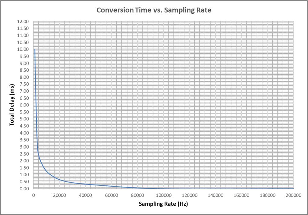
Acquisition & Conversion Time
Acquisition & Conversion Time: Total time required to obtain digital result. It consists of acquisition, decimator group delay when engaged, and IIR filter.
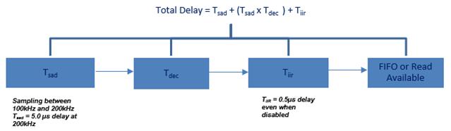
Acquisition & Conversion time will vary depending on the programmed sample rates. Expect a total delay of 5.5µs when sampling at 200kHz (max). Refer to the following chart for lower sample rates:
Latch All A/D Channels
Function: Latches all A/D channels.
Type: unsigned binary word (32-bit)
Data Range: 0x0000 0000 to 0x0000 00FF
Read/Write: R/W
Initialized Value: 0
Operational Settings: Set to 1 to latch and to 0 to unlatch. Bit-mapped per channel.
Note: The channel’s A/D Reading register will maintain the same reading while the Latch A/D bit is set to 1. Sampling for the channel will resume for that channel only when the bit is set to 0.
Latch A/D Channel
| D31 | D30 | D29 | D28 | D27 | D26 | D25 | D24 | D23 | D22 | D21 | D20 | D19 | D18 | D17 | D16 |
|---|---|---|---|---|---|---|---|---|---|---|---|---|---|---|---|
| 0 | 0 | 0 | 0 | 0 | 0 | 0 | 0 | 0 | 0 | 0 | 0 | 0 | 0 | 0 | 0 |
| D15 | D14 | D13 | D12 | D11 | D10 | D9 | D8 | D7 | D6 | D5 | D4 | D3 | D2 | D1 | D0 |
| 0 | 0 | 0 | 0 | 0 | 0 | 0 | 0 | Ch8 | Ch7 | Ch6 | Ch5 | Ch4 | Ch3 | Ch2 | Ch1 |
A/D Test Registers
Three different tests, one on-line (CBIT) and two off-line (UBIT, IBIT), can be selected. External reference voltage is not required for any of these tests.
Test Enabled
Function: Sets bit to enable the associated Built-In Self-Test (BIST): IBIT, CBIT and UBIT.
Type: unsigned binary word (32-bit)
Data Range: 0x0000 0000 to 0x0000 000F
Read/Write: R/W
Initialized Value: 0x4 (CBIT Test Enabled)
Operational Settings: BIT tests include an on-line (CBIT) test and two off-line (UBIT, IBIT) tests. Failures in the BIT test are reflected in the BIT Status registers for the corresponding channels that fail. In addition, an interrupt (if enabled in the BIT Interrupt Enable register) can be triggers when the BIT testing detects failures.
Test Enabled
| D31 | D30 | D29 | D28 | D27 | D26 | D25 | D24 | D23 | D22 | D21 | D20 | D19 | D18 | D17 | D16 |
|---|---|---|---|---|---|---|---|---|---|---|---|---|---|---|---|
| 0 | 0 | 0 | 0 | 0 | 0 | 0 | 0 | 0 | 0 | 0 | 0 | 0 | 0 | 0 | 0 |
| D15 | D14 | D13 | D12 | D11 | D10 | D9 | D8 | D7 | D6 | D5 | D4 | D3 | D2 | D1 | D0 |
| 0 | 0 | 0 | 0 | 0 | 0 | 0 | 0 | 0 | 0 | 0 | 0 | IBIT Test D | CBIT Test 1 | 0 | UBIT Test D |
UBIT Test Data
Function: Specifies voltage to be applied for the A/D UBIT off-line test.
Type: signed binary word (32-bit)
Data Range: Voltage and Current values are dependent on Polarity and Range settings for the channel.
 Unipolar: 0x0000 to 0x0000 FFFF

 Bipolar (2's compliment. 16-bit value sign extended to 32 bits): 0xFFFF 8000 to 0x0000 7FFF
Read/Write: R/W
Initialized Value: 0
Operational Settings: LSB is dependent on the Range setting. Refer to section Appendix A: Integer/Floating Point Mode Programming for Integer and Floating Point Mode examples.
FIFO Registers
The FIFO registers are configurable for each channel.
FIFO Buffer Data
Function: Available data in the FIFO buffer can be retrieved, one word at a time. (LSB for 16-bit word resolution is dependent on the Polarity and Range setting).
Type: signed binary word (32-bit) or Single Precision Floating Point Value (IEEE-754) (Floating Point Mode)
Data Range:
 Enable Floating Point Mode: 0 (Integer Mode)

      Unipolar: 0x0000 0000 to 0x0000 FFFF

      Bipolar (2's complement. 16-bit value sign extended to 32 bits): 0xFFFF 8000 to 0x0000 7FFF

 Enable Floating Point Mode: 1 (Floating Point Mode)

      Single Precision Floating Point Value (IEEE-754)
Read/Write: R
Initialized Value: N/A
Operational Settings: Refer to section Appendix A: Integer/Floating Point Mode Programming for Integer and Floating Point Mode examples.
FIFO Word Count
Function: This is a counter that reports the number of 16-bit words stored in the FIFO buffer.
Type: unsigned binary word (32-bit)
Data Range: 0x0000 0000 to 0x000F FFFF
Read/Write: R
Initialized Value: 0
Operational Settings: Every time a read operation is made from the A/D Data memory address, its corresponding Words in FIFO counter will be decremented by one. The maximum number of words that can be stored in the FIFO is 1 mega words.
FIFO Thresholds
The FIFO Almost Empty, FIFO Low Watermark, FIFO High Watermark, FIFO Almost Full and FIFO Buffer Size sets the threshold limits that are used to set the bits in the FIFO Status register.
FIFO Almost Empty
Function: The FIFO Almost Empty is used to set the limits for the “almost empty” status.
Type: unsigned binary word (32-bit)
Data Range: 0x0000 0000 to 0x000F FFFF
Read/Write: R/W
Initialized Value: 0
Operational Settings: When the Words in FIFO counter is greater than or equal to the value stored in the FIFO Almost Empty register, the “almost empty” bit (D1) of the FIFO Status register will be set. When the Words in FIFO counter is less than the value stored in the register, the “almost empty” bit (D1) of the FIFO Status register will be reset.
FIFO Low Watermark
Function: The FIFO Low Watermark (low-threshold level) is used to set the limits for the “low watermark” status.
Type: unsigned binary word (32-bit)
Data Range: 0x0000 0000 to 0x000F FFFF
Read/Write: R/W
Initialized Value: 0
Operational Settings: When the Words in FIFO counter is less than or equal to the value stored in the FIFO Low Watermark register, the “low watermark” bit (D2) of the FIFO Status register will be set. When the Words in FIFO counter is greater than the value stored in the register, the “low watermark” bit (D2) of the FIFO Status register will be reset.
FIFO High Watermark
Function: The FIFO High Watermark (high-threshold level) is used to set the limits for the “high watermark” status.
Type: unsigned binary word (32-bit)
Data Range: 0x0000 0000 to 0x000F FFFF
Read/Write: R/W
Initialized Value: 0
Operational Settings: When the Words in FIFO counter is greater than or equal to the value stored in the FIFO High Watermark register, the “high watermark” bit (D3) of the FIFO Status register will be set. When the Words in FIFO counter is less than the value stored in the high threshold, the “high watermark” bit (D3) of the FIFO Status register will be reset.
FIFO Almost Full
Function: The FIFO Almost Full is used to set the limits for the “almost full” status.
Type: unsigned binary word (32-bit)
Data Range: 0x0000 0000 to 0x000F FFFF
Read/Write: R/W
Initialized Value: 0
Operational Settings: When the Words in FIFO counter is greater than or equal to the value stored in the FIFO Almost Full register, the “almost full” bit (D4) of the FIFO Status register will be set. When the Words in FIFO counter is less than the value stored in the register, the “almost full” bit (D4) of the FIFO Status register will be reset.
FIFO Buffer Size
Function: Sets the number of samples to be taken and placed into the FIFO when a trigger occurs.
Type: unsigned binary word (32-bit)
Data Range: 0x0000 0000 to 0x000F FFFF
Read/Write: R/W
Initialized Value: 0x000F FFFF
Operational Settings: The size of each sample (number of words written to the FIFO per sample) is determined by the sample format described by the FIFO Buffer Control register. When the Words in FIFO counter reaches the FIFO Buffer Size, the “sample done” bit (D6) is set and no additional samples will be placed in the FIFO. When Words in FIFO counter is less than FIFO Buffer Size, the “sample done” bit (D6) will be reset.
Data Control
Function: Sets the format of the samples to be stored in the FIFO buffer which is determined by the bitmapped table.
Type: unsigned binary word (32-bit)
Data Range: 0x0000 0000 to 0x0000 0014
Read/Write: R/W
Initialized Value: 0
Operational Settings: The Time Stamp data format (D4) requires one word of storage space from the FIFO buffer. For example, if (D4) is set to 0 and the FIFO Buffer Size register is set to 1, a FIFO write will put one word of data in the FIFO memory space per sample and discard the timestamp. Since the maximum physical size of FIFO is 1M words for each channel, the value in the FIFO Buffer Size and Data Control registers could cause an overflow to the FIFO buffer. When an overflow condition occurs, any data that is not place in the FIFO will be lost.
| Bit | Description |
|---|---|
| D31-D5 | Reserved. Set to 0 |
| D4 | Time Stamp. An integer counter that counts from 0 to 65,535 and wraps around when it overflows. |
| D3 | Reserved. Set to 0 |
| D2 | Data Type. 0 = Raw (unfiltered); 1 = Filtered (post-programmable IIR). |
| D1 | Reserved. Set to 0 |
| D0 | Reserved. Set to 0 |
FIFO Sample Delay
Function: Sets the number of delay samples before the actual FIFO data collection begins.
Type: unsigned binary word (32-bit)
Data Range: 0x0000 0000 to 0xFFFF FFFF
Read/Write: R/W
Initialized Value: 0
Operational Settings: The data collected during the delay period will be discarded.
FIFO Skip Count
Type: unsigned binary word (32-bit)
Data Range: 0x0000 0000 to 0xFFFF FFFF
Read/Write: R/W
Initialized Value: 0 (No Skip Count (FIFO stores every sample))
Operational Settings: If the sample rate for a channel is 10 kHz, there would be a new sample every 100µs. By setting the FIFO skip count to 1, the FIFO will store a new sample every 200 µs, or at a 5 kHz rate.
Clear FIFO
Type: unsigned binary word (32-bit)
Data Range: 0 or 1
Read/Write: W
Initialized Value: N/A
Operational Settings: This resets the Words in FIFO to zero; Clear FIFO register does not clear data in the buffer. A read to the buffer data will give “aged” data. Write a 1 to reset the Words in FIFO for the channel.
| Bit | Description |
|---|---|
| D31-D1 | Reserved. Set to 0 |
| D0 | Set to 1 to Clear FIFO (i.e. reset the Words in FIFO). |
Clear FIFO
| D31 | D30 | D29 | D28 | D27 | D26 | D25 | D24 | D23 | D22 | D21 | D20 | D19 | D18 | D17 | D16 |
|---|---|---|---|---|---|---|---|---|---|---|---|---|---|---|---|
| 0 | 0 | 0 | 0 | 0 | 0 | 0 | 0 | 0 | 0 | 0 | 0 | 0 | 0 | 0 | 0 |
| D15 | D14 | D13 | D12 | D11 | D10 | D9 | D8 | D7 | D6 | D5 | D4 | D3 | D2 | D1 | D0 |
| 0 | 0 | 0 | 0 | 0 | 0 | 0 | 0 | 0 | 0 | 0 | 0 | 0 | 0 | 0 | D |
FIFO Trigger Control
Type: unsigned binary word (32-bit)
Data Range: 0x0 to 0x1FF
Read/Write: R/W
Initialized Value: 0 (Disable Trigger)
Operational Settings: For the current implementation, triggering of FIFO is by Software Trigger only. Hardware triggering will be implemented in a future release. Hardware triggering will be platform dependent based on pin-outs and I/O availability. See the tables that follow for the current and pending settings.
| D8 | Trigger Enable |
|---|---|
| 0 | Not Enabled / Stop Trigger |
| 1 | Enable Trigger |
| D[5..4] | Trigger Edge |
|---|---|
| 0 | RESERVED for Hardware Trigger (Positive Edge) |
| 1 | RESERVED for Hardware Trigger (Negative Edge) |
| 2 | RESERVED for Hardware Trigger (Either Edge) |
| 3 | Software Trigger |
| D[1..0] | Trigger Type |
|---|---|
| 0 | Continuous |
| 1 | Single Sample |
| 2 | X (Don’t care) |
| 3 | X (Don’t care) |
| D[8..0] | Summary Description |
|---|---|
| 0x130 | Store continuously once there is a Software Trigger. |
| 0x131 | Store single sample once there is a Software Trigger |
| 0x0XX | Disable Trigger (will stop FIFO from storing data if continuously running) |
FIFO Trigger Control
| D31 | D30 | D29 | D28 | D27 | D26 | D25 | D24 | D23 | D22 | D21 | D20 | D19 | D18 | D17 | D16 |
|---|---|---|---|---|---|---|---|---|---|---|---|---|---|---|---|
| 0 | 0 | 0 | 0 | 0 | 0 | 0 | 0 | 0 | 0 | 0 | 0 | 0 | 0 | 0 | 0 |
| D15 | D14 | D13 | D12 | D11 | D10 | D9 | D8 | D7 | D6 | D5 | D4 | D3 | D2 | D1 | D0 |
| 0 | 0 | 0 | 0 | 0 | 0 | 0 | D | D | D | D | D | D | D | D | D |
FIFO Software Trigger
Type: unsigned binary word (32-bit)
Data Range: 0 or 1
Read/Write: W
Initialized Value: 0 (Not Triggered)
Operational Settings: To use this operation, the FIFO Trigger Control register must be set up as described in the FIFO Trigger Control register. Write a 1 to trigger FIFO collection for all channels.
| Bit | Description |
|---|---|
| D31-D1 | Reserved. Set to 0 |
| D0 | Set to 1 to start the FIFO data collection. |
FIFO Software Trigger
| D31 | D30 | D29 | D28 | D27 | D26 | D25 | D24 | D23 | D22 | D21 | D20 | D19 | D18 | D17 | D16 |
|---|---|---|---|---|---|---|---|---|---|---|---|---|---|---|---|
| 0 | 0 | 0 | 0 | 0 | 0 | 0 | 0 | 0 | 0 | 0 | 0 | 0 | 0 | 0 | 0 |
| D15 | D14 | D13 | D12 | D11 | D10 | D9 | D8 | D7 | D6 | D5 | D4 | D3 | D2 | D1 | D0 |
| 0 | 0 | 0 | 0 | 0 | 0 | 0 | 0 | 0 | 0 | 0 | 0 | 0 | 0 | 0 | D |
Threshold Detect Programming Registers
The Analog-to-Digital function provide registers that support threshold detection. Refer to “Analog-to-Digital Threshold and Saturation Programming Module Manual” for the register descriptions.
Saturation Programming Registers
The Analog-to-Digital function provide registers that support saturation detection. Refer to “Analog-to-Digital Threshold and Saturation Programming Module Manual” for the register descriptions.
Engineering Scaling Conversions Registers
The A/D Module Threshold, Saturation, and Measurement registers can be programmed to be utilized as a Single Precision Floating Point Value (IEEE-754) or as a 32-bit integer value.
Enable Floating Point Mode
Function: Sets all channels for floating point mode or integer module.
Type: unsigned binary word (32-bit)
Data Range: 0 or 1
Read/Write: R/W
Initialized Value: 0 (Integer mode)
Operational Settings: Set bit to 1 to enable Floating Point Mode and 0 for Integer Mode. Refer to section Appendix A: Integer/Floating Point Mode Programming for Integer and Floating Point Mode examples.
Enable Floating Point Mode
| D31 | D30 | D29 | D28 | D27 | D26 | D25 | D24 | D23 | D22 | D21 | D20 | D19 | D18 | D17 | D16 |
|---|---|---|---|---|---|---|---|---|---|---|---|---|---|---|---|
| 0 | 0 | 0 | 0 | 0 | 0 | 0 | 0 | 0 | 0 | 0 | 0 | 0 | 0 | 0 | 0 |
| D15 | D14 | D13 | D12 | D11 | D10 | D9 | D8 | D7 | D6 | D5 | D4 | D3 | D2 | D1 | D0 |
| 0 | 0 | 0 | 0 | 0 | 0 | 0 | 0 | 0 | 0 | 0 | 0 | 0 | 0 | 0 | D |
Floating Point Offset
Type: Single Precision Floating Point Value (IEEE-754)
Data Range: N/A
Read/Write: R/W
Initialized Value: 0.0
Operational Settings: Refer to section Appendix A: Integer/Floating Point Mode Programming for Integer and Floating Point Mode examples.
Floating Point Scale
Function: This register sets the floating point scale to multiply to the AD data.
Type: Single Precision Floating Point Value (IEEE-754)
Data Range: N/A
Read/Write: R/W
Initialized Value: 0.0
Operational Settings: Refer to section Appendix A: Integer/Floating Point Mode Programming for Integer and Floating Point Mode examples.
Floating Point State
Function: Indicates whether the module’s internal processing is converting the register values and internal values to the binary representation of the mode selected (Integer or Floating Point).
Type: unsigned binary word (32-bit)
Data Range: 0 to 1 Read/Write: R
Initialized Value: 0
Operational Settings: Indicates the whether the module registers are in Integer (0) or Floating Point Mode (1). When the Enable Floating Point Mode is modified, the application must wait until this register’s value matches the requested mode before changing the values of the configuration and control registers with the values in the units specified (Integer or Floating Point).
Floating Point State
| D31 | D30 | D29 | D28 | D27 | D26 | D25 | D24 | D23 | D22 | D21 | D20 | D19 | D18 | D17 | D16 |
|---|---|---|---|---|---|---|---|---|---|---|---|---|---|---|---|
| 0 | 0 | 0 | 0 | 0 | 0 | 0 | 0 | 0 | 0 | 0 | 0 | 0 | 0 | 0 | 0 |
| D15 | D14 | D13 | D12 | D11 | D10 | D9 | D8 | D7 | D6 | D5 | D4 | D3 | D2 | D1 | D0 |
| 0 | 0 | 0 | 0 | 0 | 0 | 0 | 0 | 0 | 0 | 0 | 0 | 0 | 0 | 0 | D |
Background BIT Threshold Programming Registers
The Background BIT Threshold register provides the ability to specify the minimum time before the BIT fault is reported in the BIT Status registers. The BIT Clear Count register provides the ability to reset the BIT counter used in CBIT.
Background BIT Threshold
Function: Sets BIT Threshold value (in milliseconds) to use for all channels for BIT failure indication.
Type: unsigned binary word (32-bit)
Data Range: 1 ms to 65 seconds
Read/Write: R/W
Initialized Value: 5 ms
Operational Settings: The interval at which BIT is performed is dependent and differs between module types. Rather than specifying the BIT Threshold as a “count”, the BIT Threshold is specified as a time in milliseconds. The module will convert the time specified to the BIT Threshold “count” based on the BIT interval for that module.
BIT Count Clear
Function: Resets the CBIT internal circuitry and count mechanism. Set the bit corresponding to the channel you want to clear.
Type: unsigned binary word (32-bit)
Data Range: 0x0000 0000 to 0x0000 FFFF
Read/Write: W
Initialized Value: 0
Operational Settings: Set bit to 1 for channel to resets the CBIT mechanisms. Bit is self-clearing.
Note
BIT Count Clear is a shared register between the ADE/ADF and DA2 functions. Bits D7:D0 are dedicated to the ADE/ADF functions, and bits D15:D8 are dedicated to the DA2 function.
BIT Clear Count
| D31 | D30 | D29 | D28 | D27 | D26 | D25 | D24 | D23 | D22 | D21 | D20 | D19 | D18 | D17 | D16 |
|---|---|---|---|---|---|---|---|---|---|---|---|---|---|---|---|
| 0 | 0 | 0 | 0 | 0 | 0 | 0 | 0 | 0 | 0 | 0 | 0 | 0 | 0 | 0 | 0 |
| D15 | D14 | D13 | D12 | D11 | D10 | D9 | D8 | D7 | D6 | D5 | D4 | D3 | D2 | D1 | D0 |
| DA Ch8 | DA Ch7 | DA Ch6 | DA Ch5 | DA Ch4 | DA Ch3 | DA Ch2 | DA Ch1 | AD Ch8 | AD Ch7 | AD Ch6 | AD Ch5 | AD Ch4 | AD Ch3 | AD Ch2 | AD Ch1 |
Module Common Registers
Refer to “Module Common Registers Module Manual” for the register descriptions.
Status and Interrupt Registers
The AD modules provide status registers for BIT, FIFO, Open/Over-Voltage, External Power Loss, Threshold Detect, Saturation, and Inter-FPGA Failure.
Channel Status Enable
Function: Determines whether to update the status for the channels. This feature can be used to “mask” status bits of unused channels in status registers that are bitmapped by channel.
Type: unsigned binary word (32-bit)
Data Range: 0x0000 0000 to 0x0000 FFFF (Channel Status)
Read/Write: R/W
Initialized Value: 0x0000 FFFF
Operational Settings: When the bit corresponding to a given channel in the Channel Status Enable register is not enabled (0) the status will be masked and report “0” or “no failure”. This applies to all statuses that are bitmapped by channel (BIT Status, Open/Over-Voltage Status, and Front-end Amplifier Failure Status).
Note
Channel Status Enable is a shared register between the ADE/ADF and DA2 functions. Bits D7:D0 are dedicated to the ADE/ADF functions, and bits D15:D8 are dedicated to the DA2 function.
Note
Background BIT will continue to run even if the Channel Status Enable is set to ‘0’.
Channel Status Enable
| D31 | D30 | D29 | D28 | D27 | D26 | D25 | D24 | D23 | D22 | D21 | D20 | D19 | D18 | D17 | D16 |
|---|---|---|---|---|---|---|---|---|---|---|---|---|---|---|---|
| 0 | 0 | 0 | 0 | 0 | 0 | 0 | 0 | 0 | 0 | 0 | 0 | 0 | 0 | 0 | 0 |
| D15 | D14 | D13 | D12 | D11 | D10 | D9 | D8 | D7 | D6 | D5 | D4 | D3 | D2 | D1 | D0 |
| DA Ch8 | DA Ch7 | DA Ch6 | DA Ch5 | DA Ch4 | DA Ch3 | DA Ch2 | DA Ch1 | AD Ch8 | AD Ch7 | AD Ch6 | AD Ch5 | AD Ch4 | AD Ch3 | AD Ch2 | AD Ch1 |
BIT Status
There are four registers associated with the BIT Status: Dynamic, Latched, Interrupt Enable, and Set Edge/Level Interrupt. The BIT Status register will indicate an error when the voltage read is not within the error of the set value.
Note
BIT Status is a shared register between the ADE/ADF and DA2 functions. Bits D7:D0 are dedicated to the ADE/ADF functions, and bits D15:D8 are dedicated to the DA2 function.
BIT Status
| BIT Dynamic Status | |||||||||||||||
| BIT Latched Status | |||||||||||||||
| BIT Interrupt Enable | |||||||||||||||
| BIT Set Edge/Level Interrupt | |||||||||||||||
| D31 | D30 | D29 | D28 | D27 | D26 | D25 | D24 | D23 | D22 | D21 | D20 | D19 | D18 | D17 | D16 |
| 0 | 0 | 0 | 0 | 0 | 0 | 0 | 0 | 0 | 0 | 0 | 0 | 0 | 0 | 0 | 0 |
| D15 | D14 | D13 | D12 | D11 | D10 | D9 | D8 | D7 | D6 | D5 | D4 | D3 | D2 | D1 | D0 |
| DA Ch8 | DA Ch7 | DA Ch6 | DA Ch5 | DA Ch4 | DA Ch3 | DA Ch2 | DA Ch1 | AD Ch8 | AD Ch7 | AD Ch6 | AD Ch5 | AD Ch4 | AD Ch3 | AD Ch2 | AD Ch1 |
Function: Sets the corresponding bit associated with the channel’s BIT error.
Type: unsigned binary word (32-bit)
Data Range: 0x0000 0000 to 0x0000 FFFF
Read/Write: R (Dynamic), R/W (Latched, Interrupt Enable, Edge/Level Interrupt)
Initialized Value: 0
BIT Diagnostic
Upon detection of a BIT error, the following registers provide additional information about the error:
-
Power-on BIT Error (Indicates a PBIT error that occurred on power-on. Bit will remain set until the BIT Count Clear register is written to. This register is OR’d into BIT status.)
-
Anti-Aliasing Filter Error (Indicates a common-mode range input error on the front-end voltage input circuitry. This register is OR’d into BIT status.)
-
Voltage Reading Accuracy Error (Indicates voltage reading accuracy outside of spec compared with redundant reading. This is the same as CBIT. This register is OR’d into BIT status.)
FIFO Status
There are four registers associated with the FIFO Status: Dynamic, Latched, Interrupt Enable, and Set Edge/Level Interrupt. D0-D6 is used to show the different conditions of the buffer.
| Bit | Description | Configurable? |
|---|---|---|
| D0 | Almost Full; 1 when FIFO Count >= “FIFO Almost Full” register | Yes |
| D1 | Almost Empty; 1 when FIFO Count ⇐ “FIFO Almost Empty” register | Yes |
| D2 | High Watermark; 1 when FIFO Count >= “FIFO High Watermark” register | Yes |
| D3 | Low Watermark; 1 when FIFO Count ⇐ “FIFO Low Watermark” register | Yes |
| D4 | Empty; 1 when FIFO Count = 0 | No |
| D5 | Full; 1 when FIFO Count = 1 Mega Words (0x000F FFFF) | No |
FIFO Status
| FIFO Dynamic Status | |||||||||||||||
| FIFO Latched Status | |||||||||||||||
| FIFO Interrupt Enable | |||||||||||||||
| FIFO Set Edge/Level Interrupt | |||||||||||||||
| D31 | D30 | D29 | D28 | D27 | D26 | D25 | D24 | D23 | D22 | D21 | D20 | D19 | D18 | D17 | D16 |
| 0 | 0 | 0 | 0 | 0 | 0 | 0 | 0 | 0 | 0 | 0 | 0 | 0 | 0 | 0 | 0 |
| D15 | D14 | D13 | D12 | D11 | D10 | D9 | D8 | D7 | D6 | D5 | D4 | D3 | D2 | D1 | D0 |
| 0 | 0 | 0 | 0 | 0 | 0 | 0 | 0 | D | D | D | D | D | D | D | D |
Function: Sets the corresponding bit associated with the FIFO status type; there is a separate register for each channel.
Type: binary word (32-bit)
Data Range: 0x0000 0000 to 0x0000 007F
Read/Write: R (Dynamic), R/W (Latched, Interrupt Enable, Edge/Level Interrupt)
Initialized Value: 0
Note
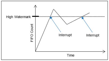
Shown below is an example of interrupts generated for the High Watermark. As shown, the interrupt is generated as the FIFO count crosses the High Watermark. The interrupt will not be generated a second time until the count goes below the watermark and then above it again.
Open/Over-Voltage Status
There are four registers associated with the Open/Over-Voltage Status: Dynamic, Latched, Interrupt Enable, and Set Edge/Level Interrupt. These registers are only applicable to ADE function.
Note
Channel 8’s negative pin (IN_CH08-) on the I/O connector MUST be tied to ground for the open detection circuitry to function properly. Failure to make this connection to ground will cause intermittent open-detect behavior on all channels.
Note
both ends of any unused channels (Pos/Neg) should be tied to the channel 8 negative pin, referred to as the Common Mode Reference Point (CMRP; isolated from system power/ground). Tying only one end of a channel, while leaving the opposing end open, may cause Open Circuit Detection to deliver unwanted voltages to your channels in use.
Open/Over-Voltage Status
| Open/Over-Voltage Dynamic Status | |||||||||||||||
| Open/Over-Voltage Latched Status | |||||||||||||||
| Open/Over-Voltage Interrupt Enable | |||||||||||||||
| Open/Over-Voltage Set Edge/Level Interrupt | |||||||||||||||
| D31 | D30 | D29 | D28 | D27 | D26 | D25 | D24 | D23 | D22 | D21 | D20 | D19 | D18 | D17 | D16 |
| 0 | 0 | 0 | 0 | 0 | 0 | 0 | 0 | Pos | Neg | Pos | Neg | Pos | Neg | Pos | Neg |
| Pos | Neg | Pos | Neg | Pos | Neg | Pos | Neg | D15 | D14 | D13 | D12 | D11 | D10 | D9 | D8 |
| D7 | D6 | D5 | D4 | D3 | D2 | D1 | D0 | Ch8 | Ch7 | Ch6 | Ch5 | Ch4 | Ch3 | Ch2 | Ch1 |
| Pos | Neg | Pos | Neg | Pos | Neg | Pos | Neg | Pos | Neg | Pos | Neg | Pos | Neg | Pos | Neg |
Function: Sets the corresponding bit associated with the channel’s Open/Over-Voltage error.
Type: unsigned binary word (32-bit)
Data Range: 0x0000 0000 to 0x0000 FFFF
Read/Write: R (Dynamic), R/W (Latched, Interrupt Enable, Edge/Level Interrupt)
Initialized Value: 0
External Power Loss Status
There are four registers associated with the External Power Loss Status: Dynamic, Latched, Interrupt Enable, and Set Edge/Level Interrupt.
D0 = +12V External Power Loss
D1 = -12V External Power Loss
External Power Loss Status
| External Power Loss Dynamic Status | |||||||||||||||
| External Power Loss Latched Status | |||||||||||||||
| External Power Loss Interrupt Enable | |||||||||||||||
| External Power Loss Set Edge/Level Interrupt | |||||||||||||||
| D31 | D30 | D29 | D28 | D27 | D26 | D25 | D24 | D23 | D22 | D21 | D20 | D19 | D18 | D17 | D16 |
| 0 | 0 | 0 | 0 | 0 | 0 | 0 | 0 | 0 | 0 | 0 | 0 | 0 | 0 | 0 | 0 |
| D15 | D14 | D13 | D12 | D11 | D10 | D9 | D8 | D7 | D6 | D5 | D4 | D3 | D2 | D1 | D0 |
| 0 | 0 | 0 | 0 | 0 | 0 | 0 | 0 | 0 | 0 | 0 | 0 | 0 | 0 | -12V | +12V |
Function: Sets the corresponding bit associated with the channel’s External Power Loss error.
Type: unsigned binary word (32-bit)
Data Range: 0x0000 0000 to 0x0000 0003
Read/Write: R (Dynamic), R/W (Latched, Interrupt Enable, Edge/Level Interrupt) Initialized Value: 0
Threshold Detect Status
The Analog-to-Digital function provide registers that support threshold detection. Refer to “Analog-to-Digital Threshold and Saturation Programming Module Manual” for the register descriptions.
Saturation Status
The Analog-to-Digital function provide registers that support saturation detection. Refer to “Analog-to-Digital Threshold and Saturation Programming Module Manual” for the register descriptions.
Front-End Amplifier Failure Status
There are four registers associated with the Front-end Amplifier Failure Status: Dynamic, Latched, Interrupt Enable, and Set Edge/Level Interrupt. These registers are only applicable to the ADF function.
Front-End Amplifier Failure Status
| Front-end Amplifier Failure Dynamic Status | |||||||||||||||
| Front-end Amplifier Failure Latched Status | |||||||||||||||
| Front-end Amplifier Failure Interrupt Enable | |||||||||||||||
| Front-end Amplifier Failure Set Edge/Level Interrupt | |||||||||||||||
| D31 | D30 | D29 | D28 | D27 | D26 | D25 | D24 | D23 | D22 | D21 | D20 | D19 | D18 | D17 | D16 |
| 0 | 0 | 0 | 0 | 0 | 0 | 0 | 0 | 0 | 0 | 0 | 0 | 0 | 0 | 0 | 0 |
| D15 | D14 | D13 | D12 | D11 | D10 | D9 | D8 | D7 | D6 | D5 | D4 | D3 | D2 | D1 | D0 |
| 0 | 0 | 0 | 0 | 0 | 0 | 0 | 0 | Ch8 | Ch7 | Ch6 | Ch5 | Ch4 | Ch3 | Ch2 | Ch1 |
Function: Sets the corresponding bit associated with the channel’s Front-end Amplifier Failure error.
Type: unsigned binary word (32-bit)
Data Range: 0x0000 0000 to 0x0000 00FF
Read/Write: R (Dynamic), R/W (Latched, Interrupt Enable, Edge/Level Interrupt) Initialized Value: 0
Inter-FPGA Failure Status
Data is periodically transferred between the Lattice FPGA and the Xilinx FPGA. A CRC value is calculated and verified with each data transfer. A CRC error flag is sent from the Lattice FPGA to the Xilinx FPGA if a CRC error is detected. The Xilinx FPGA contains a counter that will increase by two when a CRC error is flagged and decremented by one when there is no CRC error. If the counter reaches ten, the Xilinx FPGA will set the Inter-FPGA Failure status bit and shut down the isolated power supply. To recover from an Inter-FPGA Failure, the module needs to be reset and re-initialized.
There are four registers associated with the Inter-FPGA Status: Dynamic, Latched, Interrupt Enable, and Set Edge/Level Interrupt. 0 = Normal; 0xFFFF = Inter-FPGA Communication Failure. The status represents the status for all channels on the module.
Note
Inter-FPGA Failure Status is a shared register between the ADE/ADF and DA2 functions. Bits D7:D0 are dedicated to the ADE/ADF functions, and bits D15:D8 are dedicated to the DA2 function.
Inter-FPGA Failure Status
| Inter-FPGA Failure Dynamic Status | |||||||||||||||
| Inter-FPGA Failure Latched Status | |||||||||||||||
| Inter-FPGA Failure Interrupt Enable | |||||||||||||||
| Inter-FPGA Failure Set Edge/Level Interrupt | |||||||||||||||
| D31 | D30 | D29 | D28 | D27 | D26 | D25 | D24 | D23 | D22 | D21 | D20 | D19 | D18 | D17 | D16 |
| 0 | 0 | 0 | 0 | 0 | 0 | 0 | 0 | 0 | 0 | 0 | 0 | 0 | 0 | 0 | 0 |
| D15 | D14 | D13 | D12 | D11 | D10 | D9 | D8 | D7 | D6 | D5 | D4 | D3 | D2 | D1 | D0 |
| DA Ch8 | DA Ch7 | DA Ch6 | DA Ch5 | DA Ch4 | DA Ch3 | DA Ch2 | DA Ch1 | AD Ch8 | AD Ch7 | AD Ch6 | AD Ch5 | AD Ch4 | AD Ch3 | AD Ch2 | AD Ch1 |
Function: Sets the corresponding bit associated with the channel’s Inter-FPGA Failure error.
Type: unsigned binary word (32-bit)
Data Range: 0x0000 0000 to 0x0000 FFFF
Read/Write: R (Dynamic), R/W (Latched, Interrupt Enable, Edge/Level Interrupt)
Initialized Value: 0
Interrupt Vector and Steering
When interrupts are enabled, the interrupt vector associated with the specific interrupt can be programmed (typically with a unique number/identifier) such that it can be utilized in the Interrupt Service Routine (ISR) to identify the type of interrupt. When an interrupt occurs, the contents of the Interrupt Vector registers is reported as part of the interrupt mechanism.
In addition to specifying the interrupt vector, the interrupt can be directed (“steered”) to the native bus or to the application running on the onboard ARM processor.
Note
the Interrupt Vector and Interrupt Steering registers are mapped to the Motherboard Common Memory and these registers are associated with the Module Slot position (refer to Function Register Map).
Interrupt Vector
Function: Set an identifier for the interrupt.
Type: unsigned binary word (32-bit)
Data Range: 0x0000 0000 to 0xFFFF FFFF
Read/Write: R/W
Initialized Value: 0
Operational Settings: When an interrupt occurs, this value is reported as part of the interrupt mechanism.
Interrupt Steering
Function: Sets where to direct the interrupt.
Type: unsigned binary word (32-bit)
Data Range: See table
Read/Write: R/W
Initialized Value: 0
Operational Settings: When an interrupt occurs, the interrupt is sent as specified:
| Direct Interrupt to VME | 1 |
|---|---|
| Direct Interrupt to ARM Processor (via SerDes) (Custom App on ARM or NAI Ethernet Listener App) | 2 |
| Direct Interrupt to PCIe Bus | 5 |
| Direct Interrupt to cPCI Bus | 6 |
Function Register Map
Key:
Bold Italic = Configuration/Control
Bold Underline = Measurement/Status
*When an event is detected, the bit associated with the event is set in this register and will remain set until the user clears the event bit. Clearing the bit requires writing a 1 back to the specific bit that was set when read (i.e., write-1-to-clear, writing a “1” to a bit set to “1” will set the bit to “0).
**Data is represented in Floating Point if Enable Floating Point Mode register is set to Floating Point Mode (1).
~ Data is always in Floating Point.
A/D Measurement Registers
| 0x1000 | A/D Reading Ch 1** | R |
|---|---|---|
| 0x1004 | A/D Reading Ch 2** | R |
| 0x1008 | A/D Reading Ch 3** | R |
| 0x100C | A/D Reading Ch 4** | R |
| 0x1010 | A/D Reading Ch 5** | R |
| 0x1014 | A/D Reading Ch 6** | R |
| 0x1018 | A/D Reading Ch 7** | R |
| 0x101C | A/D Reading Ch 8** | R |
A/D Control Registers
| 0x1080 | Polarity & Range Ch 1 | R/W |
|---|---|---|
| 0x1084 | Polarity & Range Ch 2 | R/W |
| 0x1088 | Polarity & Range Ch 3 | R/W |
| 0x108C | Polarity & Range Ch 4 | R/W |
| 0x1090 | Polarity & Range Ch 5 | R/W |
| 0x1094 | Polarity & Range Ch 6 | R/W |
| 0x1098 | Polarity & Range Ch 7 | R/W |
| 0x109C | Polarity & Range Ch 8 | R/W |
| 0x1100 | Filter Break Frequency Ch 1 | R/W |
|---|---|---|
| 0x1104 | Filter Break Frequency Ch 2 | R/W |
| 0x1108 | Filter Break Frequency Ch 3 | R/W |
| 0x110C | Filter Break Frequency Ch 4 | R/W |
| 0x1110 | Filter Break Frequency Ch 5 | R/W |
| 0x1114 | Filter Break Frequency Ch 6 | R/W |
| 0x1118 | Filter Break Frequency Ch 7 | R/W |
| 0x111C | Filter Break Frequency Ch 8 | R/W |
| 0x188C | Sample Rate | R/W |
|---|
| 0x1880 | Latch All A/D Channels | R/W |
|---|
FIFO Registers
| 0x1180 | FIFO Buffer Data Ch 1**** | R |
|---|---|---|
| 0x1184 | FIFO Buffer Data Ch 2**** | R |
| 0x1188 | FIFO Buffer Data Ch 3**** | R |
| 0x118C | FIFO Buffer Data Ch 4**** | R |
| 0x1190 | FIFO Buffer Data Ch 5**** | R |
| 0x1194 | FIFO Buffer Data Ch 6**** | R |
| 0x1198 | FIFO Buffer Data Ch 7**** | R |
| 0x119C | FIFO Buffer Data Ch 8**** | R |
| 0x1200 | FIFO Word Count Ch 1 | R |
|---|---|---|
| 0x1204 | FIFO Word Count Ch 2 | R |
| 0x1208 | FIFO Word Count Ch 3 | R |
| 0x120C | FIFO Word Count Ch 4 | R |
| 0x1210 | FIFO Word Count Ch 5 | R |
| 0x1214 | FIFO Word Count Ch 6 | R |
| 0x1218 | FIFO Word Count Ch 7 | R |
| 0x121C | FIFO Word Count Ch 8 | R |
| 0x1480 | FIFO Sample Delay Ch 1 | R/W |
|---|---|---|
| 0x1484 | FIFO Sample Delay Ch 2 | R/W |
| 0x1488 | FIFO Sample Delay Ch 3 | R/W |
| 0x148C | FIFO Sample Delay Ch 4 | R/W |
| 0x1490 | FIFO Sample Delay Ch 5 | R/W |
| 0x1494 | FIFO Sample Delay Ch 6 | R/W |
| 0x1498 | FIFO Sample Delay Ch 7 | R/W |
| 0x149C | FIFO Sample Delay Ch 8 | R/W |
| 0x1580 | FIFO Skip Count Ch 1 | R/W |
|---|---|---|
| 0x1584 | FIFO Skip Count Ch 2 | R/W |
| 0x1588 | FIFO Skip Count Ch 3 | R/W |
| 0x158C | FIFO Skip Count Ch 4 | R/W |
| 0x1590 | FIFO Skip Count Ch 5 | R/W |
| 0x1594 | FIFO Skip Count Ch 6 | R/W |
| 0x1598 | FIFO Skip Count Ch 7 | R/W |
| 0x159C | FIFO Skip Count Ch 8 | R/W |
| 0x1600 | Clear FIFO Ch 1 | W |
|---|---|---|
| 0x1604 | Clear FIFO Ch 2 | W |
| 0x1608 | Clear FIFO Ch 3 | W |
| 0x160C | Clear FIFO Ch 4 | W |
| 0x1610 | Clear FIFO Ch 5 | W |
| 0x1614 | Clear FIFO Ch 6 | W |
| 0x1618 | Clear FIFO Ch 7 | W |
| 0x161C | Clear FIFO Ch 8 | W |
| 0x1680 | Data Control Ch 1 | R/W |
|---|---|---|
| 0x1684 | Data Control Ch 2 | R/W |
| 0x1688 | Data Control Ch 3 | R/W |
| 0x168C | Data Control Ch 4 | R/W |
| 0x1690 | Data Control Ch 5 | R/W |
| 0x1694 | Data Control Ch 6 | R/W |
| 0x1698 | Data Control Ch 7 | R/W |
| 0x169C | Data Control Ch 8 | R/W |
| 0x1884 | FIFO Trigger Control | R/W |
|---|---|---|
| 0x1888 | FIFO Software Trigger | W |
FIFO Threshold
| 0x1280 | FIFO Almost Empty Ch 1 | R/W |
|---|---|---|
| 0x1284 | FIFO Almost Empty Ch 2 | R/W |
| 0x1288 | FIFO Almost Empty Ch 3 | R/W |
| 0x128C | FIFO Almost Empty Ch 4 | R/W |
| 0x1290 | FIFO Almost Empty Ch 5 | R/W |
| 0x1294 | FIFO Almost Empty Ch 6 | R/W |
| 0x1298 | FIFO Almost Empty Ch 7 | R/W |
| 0x129C | FIFO Almost Empty Ch 8 | R/W |
| 0x1380 | FIFO Low Watermark Ch 1 | R/W |
|---|---|---|
| 0x1384 | FIFO Low Watermark Ch 2 | R/W |
| 0x1388 | FIFO Low Watermark Ch 3 | R/W |
| 0x138C | FIFO Low Watermark Ch 4 | R/W |
| 0x1390 | FIFO Low Watermark Ch 5 | R/W |
| 0x1394 | FIFO Low Watermark Ch 6 | R/W |
| 0x1398 | FIFO Low Watermark Ch 7 | R/W |
| 0x139C | FIFO Low Watermark Ch 8 | R/W |
| 0x1300 | FIFO Almost Full Ch 1 | R/W |
|---|---|---|
| 0x1304 | FIFO Almost Full Ch 2 | R/W |
| 0x1308 | FIFO Almost Full Ch 3 | R/W |
| 0x130C | FIFO Almost Full Ch 4 | R/W |
| 0x1310 | FIFO Almost Full Ch 5 | R/W |
| 0x1314 | FIFO Almost Full Ch 6 | R/W |
| 0x1318 | FIFO Almost Full Ch 7 | R/W |
| 0x131C | FIFO Almost Full Ch 8 | R/W |
| 0x1400 | FIFO High Watermark Ch 1 | R/W |
|---|---|---|
| 0x1404 | FIFO High Watermark Ch 2 | R/W |
| 0x1408 | FIFO High Watermark Ch 3 | R/W |
| 0x140C | FIFO High Watermark Ch 4 | R/W |
| 0x1410 | FIFO High Watermark Ch 5 | R/W |
| 0x1414 | FIFO High Watermark Ch 6 | R/W |
| 0x1418 | FIFO High Watermark Ch 7 | R/W |
| 0x141C | FIFO High Watermark Ch 8 | R/W |
| 0x1500 | FIFO Buffer Size Ch 1 | R/W |
|---|---|---|
| 0x1504 | FIFO Buffer Size Ch 2 | R/W |
| 0x1508 | FIFO Buffer Size Ch 3 | R/W |
| 0x150C | FIFO Buffer Size Ch 4 | R/W |
| 0x1510 | FIFO Buffer Size Ch 5 | R/W |
| 0x1514 | FIFO Buffer Size Ch 6 | R/W |
| 0x1518 | FIFO Buffer Size Ch 7 | R/W |
| 0x151C | FIFO Buffer Size Ch 8 | R/W |
Threshold Detect Programming Registers
The Analog-to-Digital function provide registers that support threshold detection. Refer to “Analog-to-Digital Threshold and Saturation Programming Module Manual” for the Threshold Detect Programming Function Register Map.
Saturation Programming Registers
The Analog-to-Digital function provide registers that support saturation detection. Refer to “Analog-to-Digital Threshold and Saturation Programming Module Manual” for the Saturation Programming Function Register Map.
Engineering Scaling Conversions Registers
| 0x02B4 | Enable Floating Point | R/W |
|---|---|---|
| 0x0264 | Floating Point State | R |
| 0x1700 | Floating Point Offset Ch 1~ | R/W |
|---|---|---|
| 0x1704 | Floating Point Offset Ch 2~ | R/W |
| 0x1708 | Floating Point Offset Ch 3~ | R/W |
| 0x170C | Floating Point Offset Ch 4~ | R/W |
| 0x1710 | Floating Point Offset Ch 5~ | R/W |
| 0x1714 | Floating Point Offset Ch 6~ | R/W |
| 0x1718 | Floating Point Offset Ch 7~ | R/W |
| 0x171C | Floating Point Offset Ch 8~ | R/W |
| 0x1780 | Floating Point Scale Ch 1~ | R/W |
|---|---|---|
| 0x1784 | Floating Point Scale Ch 2~ | R/W |
| 0x1788 | Floating Point Scale Ch 3~ | R/W |
| 0x178C | Floating Point Scale Ch 4~ | R/W |
| 0x1790 | Floating Point Scale Ch 5~ | R/W |
| 0x1794 | Floating Point Scale Ch 6~ | R/W |
| 0x1798 | Floating Point Scale Ch 7~ | R/W |
| 0x179C | Floating Point Scale Ch 8~ | R/W |
Module Common Registers
Refer to “Module Common Registers Module Manual” for the Module Common Registers Function Register Map.
A/D Status Registers
| 0x02B0 | Channel Status Enable | R/W |
|---|
BIT Registers
| 0x0800 | Dynamic Status | R |
|---|---|---|
| 0x0804 | Latched Status* | R/W |
| 0x0808 | Interrupt Enable | R/W |
| 0x080C | Set Edge/Level Interrupt | R/W |
| 0x1804 | Anti-Aliasing Filter Error | R |
|---|---|---|
| 0x1808 | Voltage Reading Accuracy Error | R |
| 0x0248 | Test Enabled | R/W |
|---|---|---|
| 0x024C | Test CBIT Verify | R/W |
| 0x0294 | UBIT Polarity | R/W |
| 0x0298 | UBIT Test Data | R/W |
| 0x02B8 | Background BIT Threshold | R/W |
|---|---|---|
| 0x02BC | BIT Count Clear | W |
| 0x02AC | Power-on BIT Complete++ | R |
|---|---|---|
| 0x1800 | Power-on BIT Error | R |
++After power-on, Power-on BIT Complete should be checked before reading the BIT Latched Status.
Open/Over-Voltage Status - ADE
| 0x08A0 | Dynamic Status | R |
|---|---|---|
| 0x08A4 | Latched Status* | R/W |
| 0x08A8 | Interrupt Enable | R/W |
| 0x08AC | Set Edge/Level Interrupt | R/W |
External Power Loss Status
| 0x0970 | Dynamic Status | R |
|---|---|---|
| 0x0974 | Latched Status* | R/W |
| 0x0978 | Interrupt Enable | R/W |
| 0x097C | Set Edge/Level Interrupt | R/W |
Threshold Detect Status
| 0x08B0 | Dynamic Status | R |
|---|---|---|
| 0x08B4 | Latched Status* | R/W |
| 0x08B8 | Interrupt Enable | R/W |
| 0x08BC | Set Edge/Level Interrupt | R/W |
Note
The CME/CMF module uses these registers in lieu of the threshold status registers referenced in the “Analog-to-Digital Threshold and Saturation Programming Module Manual” Function Register Map.
Front-End Amplifier - ADF
| 0x08C0 | Dynamic Status | R |
|---|---|---|
| 0x08C4 | Latched Status* | R/W |
| 0x08C8 | Interrupt Enable | R/W |
| 0x08CC | Set Edge/Level Interrupt | R/W |
Saturation Status
| 0x08D0 | Dynamic Status | R |
|---|---|---|
| 0x08D4 | Latched Status* | R/W |
| 0x08D8 | Interrupt Enable | R/W |
| 0x08DC | Set Edge/Level Interrupt | R/W |
Note
The CME/CMF module uses these registers in lieu of the saturation status registers referenced in the “Analog-to-Digital Threshold and Saturation Programming Module Manual” Function Register Map.
Inter-FPGA Failure
| 0x09B0 | Dynamic Status | R |
|---|---|---|
| 0x09B4 | Latched Status* | R/W |
| 0x09B8 | Interrupt Enable | R/W |
| 0x09BC | Set Edge/Level Interrupt | R/W |
FIFO Status
| Ch 1 | ||
| 0x0810 | Dynamic Status | R |
| 0x0814 | Latched Status* | R/W |
| 0x0818 | Interrupt Enable | R/W |
| 0x081C | Set Edge/Level Interrupt | R/W |
| Ch 2 | ||
| 0x0820 | Dynamic Status | R |
| 0x0824 | Latched Status* | R/W |
| 0x0828 | Interrupt Enable | R/W |
| 0x082C | Set Edge/Level Interrupt | R/W |
| Ch 3 | ||
| 0x0830 | Dynamic Status | R |
| 0x0834 | Latched Status* | R/W |
| 0x0838 | Interrupt Enable | R/W |
| 0x083C | Set Edge/Level Interrupt | R/W |
| Ch 4 | ||
| 0x0840 | Dynamic Status | R |
| 0x0844 | Latched Status* | R/W |
| 0x0848 | Interrupt Enable | R/W |
| 0x084C | Set Edge/Level Interrupt | R/W |
| Ch 5 | ||
| 0x0850 | Dynamic Status | R |
| 0x0854 | Latched Status* | R/W |
| 0x0858 | Interrupt Enable | R/W |
| 0x085C | Set Edge/Level Interrupt | R/W |
| Ch 6 | ||
| 0x0860 | Dynamic Status | R |
| 0x0864 | Latched Status* | R/W |
| 0x0868 | Interrupt Enable | R/W |
| 0x086C | Set Edge/Level Interrupt | R/W |
| Ch 7 | ||
| 0x0870 | Dynamic Status | R/W |
| 0x0874 | Latched Status* | R/W |
| 0x0878 | Interrupt Enable | R/W |
| 0x087C | Set Edge/Level Interrupt | R/W |
| Ch 8 | ||
| 0x0880 | Dynamic Status | R/W |
| 0x0884 | Latched Status* | R/W |
| 0x0888 | Interrupt Enable | R/W |
| 0x088C | Set Edge/Level Interrupt | R/W |
A/D Interrupt Registers
The Interrupt Vector and Interrupt Steering registers are located on the Motherboard Memory Space and do not require any Module Address Offsets. These registers are accessed using the absolute addresses listed in the table below.
| 0x0500 | Module 1 Interrupt Vector 1 - BIT | R/W |
|---|---|---|
| 0x0504 | Module 1 Interrupt Vector 2 - FIFO Ch 1 | R/W |
| 0x0508 | Module 1 Interrupt Vector 3 - FIFO Ch 2 | R/W |
| 0x050C | Module 1 Interrupt Vector 4 - FIFO Ch 3 | R/W |
| 0x0510 | Module 1 Interrupt Vector 5 - FIFO Ch 4 | R/W |
| 0x0514 | Module 1 Interrupt Vector 6 - FIFO Ch 5 | R/W |
| 0x0518 | Module 1 Interrupt Vector 7 - FIFO Ch 6 | R/W |
| 0x051C | Module 1 Interrupt Vector 8 - FIFO Ch 7 | R/W |
| 0x0520 | Module 1 Interrupt Vector 9 - FIFO Ch 8 | R/W |
| 0x0524 to 0x0544 | Module 1 Interrupt Vector 10-18 - Reserved | R/W |
| 0x0548 | Module 1 Interrupt Vector 19 - Open | R/W |
| 0x054C | Module 1 Interrupt Vector 20 - ExtPwrLoss | R/W |
| 0x0550 | Module 1 Interrupt Vector 21 - Threshold | R/W |
| 0x0554 | Module 1 Interrupt Vector 22 - Reserved | R/W |
| 0x0558 | Module 1 Interrupt Vector 23 - Saturation | R/W |
| 0x055C to 0x0568 | Module 1 Interrupt Vector 24-27 - Reserved | R/W |
| 0x056C | Module 1 Interrupt Vector 28 - Inter-FPGA | R/W |
| 0x0570 to 0x057C | Module 1 Interrupt Vector 29-32 - Reserved | R/W |
| 0x0600 | Module 1 Interrupt Steering 1 - BIT | R/W |
|---|---|---|
| 0x0604 | Module 1 Interrupt Steering 2 - FIFO Ch 1 | R/W |
| 0x0608 | Module 1 Interrupt Steering 3 - FIFO Ch 2 | R/W |
| 0x060C | Module 1 Interrupt Steering 4 - FIFO Ch 3 | R/W |
| 0x0610 | Module 1 Interrupt Steering 5 - FIFO Ch 4 | R/W |
| 0x0614 | Module 1 Interrupt Steering 6 - FIFO Ch 5 | R/W |
| 0x0618 | Module 1 Interrupt Steering 7 - FIFO Ch 6 | R/W |
| 0x061C | Module 1 Interrupt Steering 8 - FIFO Ch 7 | R/W |
| 0x0620 | Module 1 Interrupt Steering 9 - FIFO Ch 8 | R/W |
| 0x0624 to 0x0644 | Module 1 Interrupt Steering 10-18 - Reserved | R/W |
| 0x0648 | Module 1 Interrupt Steering 19 - Open | R/W |
| 0x064C | Module 1 Interrupt Steering 20 - ExtPwrLoss | R/W |
| 0x0650 | Module 1 Interrupt Steering 21 - Threshold | R/W |
| 0x0654 | Module 1 Interrupt Steering 22 - Reserved | R/W |
| 0x0658 | Module 1 Interrupt Steering 23 - Saturation | R/W |
| 0x065C to 0x0668 | Module 1 Interrupt Steering 24-27 - Reserved | R/W |
| 0x066C | Module 1 Interrupt Steering 28 - Inter-FPGA | R/W |
| 0x0670 to 0x067C | Module 1 Interrupt Steering 29-32 - Reserved | R/W |
| 0x0700 | Module 2 Interrupt Vector 1 - BIT | R/W |
|---|---|---|
| 0x0704 | Module 2 Interrupt Vector 2 - FIFO Ch 1 | R/W |
| 0x0708 | Module 2 Interrupt Vector 3 - FIFO Ch 2 | R/W |
| 0x070C | Module 2 Interrupt Vector 4 - FIFO Ch 3 | R/W |
| 0x0710 | Module 2 Interrupt Vector 5 - FIFO Ch 4 | R/W |
| 0x0714 | Module 2 Interrupt Vector 6 - FIFO Ch 5 | R/W |
| 0x0718 | Module 2 Interrupt Vector 7 - FIFO Ch 6 | R/W |
| 0x071C | Module 2 Interrupt Vector 8 - FIFO Ch 7 | R/W |
| 0x0720 | Module 2 Interrupt Vector 9 - FIFO Ch 8 | R/W |
| 0x0724 to 0x0744 | Module 2 Interrupt Vector 10-18 - Reserved | R/W |
| 0x0748 | Module 2 Interrupt Vector 19 - Open | R/W |
| 0x074C | Module 2 Interrupt Vector 20 - ExtPwrLoss | R/W |
| 0x0750 | Module 2 Interrupt Vector 21 - Threshold | R/W |
| 0x0754 | Module 2 Interrupt Vector 22 - Reserved | R/W |
| 0x0758 | Module 2 Interrupt Vector 23 - Saturation | R/W |
| 0x075C to 0x0768 | Module 2 Interrupt Vector 24-27 - Reserved | R/W |
| 0x076C | Module 2 Interrupt Vector 28 - Inter-FPGA | R/W |
| 0x0770 to 0x077C | Module 2 Interrupt Vector 29-32 - Reserved | R/W |
| 0x0800 | Module 2 Interrupt Steering 1 - BIT | R/W |
|---|---|---|
| 0x0804 | Module 2 Interrupt Steering 2 - FIFO Ch 1 | R/W |
| 0x0808 | Module 2 Interrupt Steering 3 - FIFO Ch 2 | R/W |
| 0x080C | Module 2 Interrupt Steering 4 - FIFO Ch 3 | R/W |
| 0x0810 | Module 2 Interrupt Steering 5 - FIFO Ch 4 | R/W |
| 0x0814 | Module 2 Interrupt Steering 6 - FIFO Ch 5 | R/W |
| 0x0818 | Module 2 Interrupt Steering 7 - FIFO Ch 6 | R/W |
| 0x081C | Module 2 Interrupt Steering 8 - FIFO Ch 7 | R/W |
| 0x0820 | Module 2 Interrupt Steering 9 - FIFO Ch 8 | R/W |
| 0x0824 to 0x0844 | Module 2 Interrupt Steering 10-18 - Reserved | R/W |
| 0x0848 | Module 2 Interrupt Steering 19 - Open | R/W |
| 0x084C | Module 2 Interrupt Steering 20 - ExtPwrLoss | R/W |
| 0x0850 | Module 2 Interrupt Steering 21 - Threshold | R/W |
| 0x0854 | Module 2 Interrupt Steering 22 - Reserved | R/W |
| 0x0858 | Module 2 Interrupt Steering 23 - Saturation | R/W |
| 0x085C to 0x0868 | Module 2 Interrupt Steering 24-27 - Reserved | R/W |
| 0x086C | Module 2 Interrupt Steering 28 - Inter-FPGA | R/W |
| 0x0870 to 0x087C | Module 2 Interrupt Steering 29-32 - Reserved | R/W |
| 0x0900 | Module 3 Interrupt Vector 1 - BIT | R/W |
|---|---|---|
| 0x0904 | Module 3 Interrupt Vector 2 - FIFO Ch 1 | R/W |
| 0x0908 | Module 3 Interrupt Vector 3 - FIFO Ch 2 | R/W |
| 0x090C | Module 3 Interrupt Vector 4 - FIFO Ch 3 | R/W |
| 0x0910 | Module 3 Interrupt Vector 5 - FIFO Ch 4 | R/W |
| 0x0914 | Module 3 Interrupt Vector 6 - FIFO Ch 5 | R/W |
| 0x0918 | Module 3 Interrupt Vector 7 - FIFO Ch 6 | R/W |
| 0x091C | Module 3 Interrupt Vector 8 - FIFO Ch 7 | R/W |
| 0x0920 | Module 3 Interrupt Vector 9 - FIFO Ch 8 | R/W |
| 0x0924 to 0x0944 | Module 3 Interrupt Vector 10-18 - Reserved | R/W |
| 0x0948 | Module 3 Interrupt Vector 19 - Open | R/W |
| 0x094C | Module 3 Interrupt Vector 20 - ExtPwrLoss | R/W |
| 0x0950 | Module 3 Interrupt Vector 21 - Threshold | R/W |
| 0x0954 | Module 3 Interrupt Vector 22 - Reserved | R/W |
| 0x0958 | Module 3 Interrupt Vector 23 - Saturation | R/W |
| 0x095C to 0x0968 | Module 3 Interrupt Vector 24-27 - Reserved | R/W |
| 0x096C | Module 3 Interrupt Vector 28 - Inter-FPGA | R/W |
| 0x0970 to 0x097C | Module 3 Interrupt Vector 29-32 - Reserved | R/W |
| 0x0A00 | Module 3 Interrupt Steering 1 - BIT | R/W |
|---|---|---|
| 0x0A04 | Module 3 Interrupt Steering 2 - FIFO Ch 1 | R/W |
| 0x0A08 | Module 3 Interrupt Steering 3 - FIFO Ch 2 | R/W |
| 0x0A0C | Module 3 Interrupt Steering 4 - FIFO Ch 3 | R/W |
| 0x0A10 | Module 3 Interrupt Steering 5 - FIFO Ch 4 | R/W |
| 0x0A14 | Module 3 Interrupt Steering 6 - FIFO Ch 5 | R/W |
| 0x0A18 | Module 3 Interrupt Steering 7 - FIFO Ch 6 | R/W |
| 0x0A1C | Module 3 Interrupt Steering 8 - FIFO Ch 7 | R/W |
| 0x0A20 | Module 3 Interrupt Steering 9 - FIFO Ch 8 | R/W |
| 0x0A24 to 0x0A44 | Module 3 Interrupt Steering 10-18 - Reserved | R/W |
| 0x0A48 | Module 3 Interrupt Steering 19 - Open | R/W |
| 0x0A4C | Module 3 Interrupt Steering 20 - ExtPwrLoss | R/W |
| 0x0A50 | Module 3 Interrupt Steering 21 - Threshold | R/W |
| 0x0A54 | Module 3 Interrupt Steering 22 - Reserved | R/W |
| 0x0A58 | Module 3 Interrupt Steering 23 - Saturation | R/W |
| 0x0A5C to 0x0A68 | Module 3 Interrupt Steering 24-27 - Reserved | R/W |
| 0x086C | Module 3 Interrupt Steering 28 - Inter-FPGA | R/W |
| 0x0870 to 0x087C | Module 3 Interrupt Steering 29-32 - Reserved | R/W |
| 0x0B00 | Module 4 Interrupt Vector 1 - BIT | R/W |
|---|---|---|
| 0x0B04 | Module 4 Interrupt Vector 2 - FIFO Ch 1 | R/W |
| 0x0B08 | Module 4 Interrupt Vector 3 - FIFO Ch 2 | R/W |
| 0x0B0C | Module 4 Interrupt Vector 4 - FIFO Ch 3 | R/W |
| 0x0B10 | Module 4 Interrupt Vector 5 - FIFO Ch 4 | R/W |
| 0x0B14 | Module 4 Interrupt Vector 6 - FIFO Ch 5 | R/W |
| 0x0B18 | Module 4 Interrupt Vector 7 - FIFO Ch 6 | R/W |
| 0x0B1C | Module 4 Interrupt Vector 8 - FIFO Ch 7 | R/W |
| 0x0B20 | Module 4 Interrupt Vector 9 - FIFO Ch 8 | R/W |
| 0x0B24 to 0x0B44 | Module 4 Interrupt Vector 10-18 - Reserved | R/W |
| 0x0B48 | Module 4 Interrupt Vector 19 - Open | R/W |
| 0x0B4C | Module 4 Interrupt Vector 20 - ExtPwrLoss | R/W |
| 0x0B50 | Module 4 Interrupt Vector 21 - Threshold | R/W |
| 0x0B54 | Module 4 Interrupt Vector 22 - Reserved | R/W |
| 0x0B58 | Module 4 Interrupt Vector 23 - Saturation | R/W |
| 0x0B5C to 0x0B68 | Module 4 Interrupt Vector 24-27 - Reserved | R/W |
| 0x0B6C | Module 4 Interrupt Vector 28 - Inter-FPGA | R/W |
| 0x0B70 to 0x0B7C | Module 4 Interrupt Vector 29-32 - Reserved | R/W |
| 0x0C00 | Module 4 Interrupt Steering 1 - BIT | R/W |
|---|---|---|
| 0x0C04 | Module 4 Interrupt Steering 2 - FIFO Ch 1 | R/W |
| 0x0C08 | Module 4 Interrupt Steering 3 - FIFO Ch 2 | R/W |
| 0x0C0C | Module 4 Interrupt Steering 4 - FIFO Ch 3 | R/W |
| 0x0C10 | Module 4 Interrupt Steering 5 - FIFO Ch 4 | R/W |
| 0x0C14 | Module 4 Interrupt Steering 6 - FIFO Ch 5 | R/W |
| 0x0C18 | Module 4 Interrupt Steering 7 - FIFO Ch 6 | R/W |
| 0x0C1C | Module 4 Interrupt Steering 8 - FIFO Ch 7 | R/W |
| 0x0C20 | Module 4 Interrupt Steering 9 - FIFO Ch 8 | R/W |
| 0x0C24 to 0x0C44 | Module 4 Interrupt Steering 10-18 - Reserved | R/W |
| 0x0C48 | Module 4 Interrupt Steering 19 - Open | R/W |
| 0x0C4C | Module 4 Interrupt Steering 20 - ExtPwrLoss | R/W |
| 0x0C50 | Module 4 Interrupt Steering 21 - Threshold | R/W |
| 0x0C54 | Module 4 Interrupt Steering 22 - Reserved | R/W |
| 0x0C58 | Module 4 Interrupt Steering 23 - Saturation | R/W |
| 0x0C5C to 0x0C68 | Module 4 Interrupt Steering 24-27 - Reserved | R/W |
| 0x0C6C | Module 4 Interrupt Steering 28 - Inter-FPGA | R/W |
| 0x0C70 to 0x0C7C | Module 4 Interrupt Steering 29-32 - Reserved | R/W |
| 0x0D00 | Module 5 Interrupt Vector 1 - BIT | R/W |
|---|---|---|
| 0x0D04 | Module 5 Interrupt Vector 2 - FIFO Ch 1 | R/W |
| 0x0D08 | Module 5 Interrupt Vector 3 - FIFO Ch 2 | R/W |
| 0x0D0C | Module 5 Interrupt Vector 4 - FIFO Ch 3 | R/W |
| 0x0D10 | Module 5 Interrupt Vector 5 - FIFO Ch 4 | R/W |
| 0x0D14 | Module 5 Interrupt Vector 6 - FIFO Ch 5 | R/W |
| 0x0D18 | Module 5 Interrupt Vector 7 - FIFO Ch 6 | R/W |
| 0x0D1C | Module 5 Interrupt Vector 8 - FIFO Ch 7 | R/W |
| 0x0D20 | Module 5 Interrupt Vector 9 - FIFO Ch 8 | R/W |
| 0x0D24 to 0x0D44 | Module 5 Interrupt Vector 10-18 - Reserved | R/W |
| 0x0D48 | Module 5 Interrupt Vector 19 - Open | R/W |
| 0x0D4C | Module 5 Interrupt Vector 20 - ExtPwrLoss | R/W |
| 0x0D50 | Module 5 Interrupt Vector 21 - Threshold | R/W |
| 0x0D54 | Module 5 Interrupt Vector 22 - Reserved | R/W |
| 0x0D58 | Module 5 Interrupt Vector 23 - Saturation | R/W |
| 0x0D5C to 0x0D68 | Module 5 Interrupt Vector 24-27 - Reserved | R/W |
| 0x0D6C | Module 5 Interrupt Vector 28 - Inter-FPGA | R/W |
| 0x0D70 to 0x0D7C | Module 5 Interrupt Vector 29-32 - Reserved | R/W |
| 0x0E00 | Module 5 Interrupt Steering 1 - BIT | R/W |
|---|---|---|
| 0x0E04 | Module 5 Interrupt Steering 2 - FIFO Ch 1 | R/W |
| 0x0E08 | Module 5 Interrupt Steering 3 - FIFO Ch 2 | R/W |
| 0x0E0C | Module 5 Interrupt Steering 4 - FIFO Ch 3 | R/W |
| 0x0E10 | Module 5 Interrupt Steering 5 - FIFO Ch 4 | R/W |
| 0x0E14 | Module 5 Interrupt Steering 6 - FIFO Ch 5 | R/W |
| 0x0E18 | Module 5 Interrupt Steering 7 - FIFO Ch 6 | R/W |
| 0x0E1C | Module 5 Interrupt Steering 8 - FIFO Ch 7 | R/W |
| 0x0E20 | Module 5 Interrupt Steering 9 - FIFO Ch 8 | R/W |
| 0x0E24 to 0x0E44 | Module 5 Interrupt Steering 10-18 - Reserved | R/W |
| 0x0E48 | Module 5 Interrupt Steering 19 - Open | R/W |
| 0x0E4C | Module 5 Interrupt Steering 20 - ExtPwrLoss | R/W |
| 0x0E50 | Module 5 Interrupt Steering 21 - Threshold | R/W |
| 0x0E54 | Module 5 Interrupt Steering 22 - Reserved | R/W |
| 0x0E58 | Module 5 Interrupt Steering 23 - Saturation | R/W |
| 0x0E5C to 0x0E68 | Module 5 Interrupt Steering 24-27 - Reserved | R/W |
| 0x0E6C | Module 5 Interrupt Steering 28 - Inter-FPGA | R/W |
| 0x0E70 to 0x0E7C | Module 5 Interrupt Steering 29-32 - Reserved | R/W |
| 0x0F00 | Module 6 Interrupt Vector 1 - BIT | R/W |
|---|---|---|
| 0x0F04 | Module 6 Interrupt Vector 2 - FIFO Ch 1 | R/W |
| 0x0F08 | Module 6 Interrupt Vector 3 - FIFO Ch 2 | R/W |
| 0x0F0C | Module 6 Interrupt Vector 4 - FIFO Ch 3 | R/W |
| 0x0F10 | Module 6 Interrupt Vector 5 - FIFO Ch 4 | R/W |
| 0x0F14 | Module 6 Interrupt Vector 6 - FIFO Ch 5 | R/W |
| 0x0F18 | Module 6 Interrupt Vector 7 - FIFO Ch 6 | R/W |
| 0x0F1C | Module 6 Interrupt Vector 8 - FIFO Ch 7 | R/W |
| 0x0F20 | Module 6 Interrupt Vector 9 - FIFO Ch 8 | R/W |
| 0x0F24 to 0x0F44 | Module 6 Interrupt Vector 10-18 - Reserved | R/W |
| 0x0F48 | Module 6 Interrupt Vector 19 - Open | R/W |
| 0x0F4C | Module 6 Interrupt Vector 20 - ExtPwrLoss | R/W |
| 0x0F50 | Module 6 Interrupt Vector 21 - Threshold | R/W |
| 0x0F54 | Module 6 Interrupt Vector 22 - Reserved | R/W |
| 0x0F58 | Module 6 Interrupt Vector 23 - Saturation | R/W |
| 0x0F5C to 0x0F68 | Module 6 Interrupt Vector 24-27 - Reserved | R/W |
| 0x0F6C | Module 6 Interrupt Vector 28 - Inter-FPGA | R/W |
| 0x0F70 to 0x0F7C | Module 6 Interrupt Vector 29-32 - Reserved | R/W |
| 0x1000 | Module 6 Interrupt Steering 1 - BIT | R/W |
|---|---|---|
| 0x1004 | Module 6 Interrupt Steering 2 - FIFO Ch 1 | R/W |
| 0x0E08 | Module 6 Interrupt Steering 3 - FIFO Ch 2 | R/W |
| 0x100C | Module 6 Interrupt Steering 4 - FIFO Ch 3 | R/W |
| 0x1010 | Module 6 Interrupt Steering 5 - FIFO Ch 4 | R/W |
| 0x1014 | Module 6 Interrupt Steering 6 - FIFO Ch 5 | R/W |
| 0x1018 | Module 6 Interrupt Steering 7 - FIFO Ch 6 | R/W |
| 0x101C | Module 6 Interrupt Steering 8 - FIFO Ch 7 | R/W |
| 0x1020 | Module 6 Interrupt Steering 9 - FIFO Ch 8 | R/W |
| 0x1024 to 0x1044 | Module 6 Interrupt Steering 10-18 - Reserved | R/W |
| 0x1048 | Module 6 Interrupt Steering 19 - Open | R/W |
| 0x104C | Module 6 Interrupt Steering 20 - ExtPwrLoss | R/W |
| 0x1050 | Module 6 Interrupt Steering 21 - Threshold | R/W |
| 0x1054 | Module 6 Interrupt Steering 22 - Reserved | R/W |
| 0x1058 | Module 6 Interrupt Steering 23 - Saturation | R/W |
| 0x105C to 0x1068 | Module 6 Interrupt Steering 24-27 - Reserved | R/W |
| 0x106C | Module 6 Interrupt Steering 28 - Inter-FPGA | R/W |
| 0x1070 to 0x107C | Module 6 Interrupt Steering 29-32 - Reserved | R/W |
APPENDIX A: INTEGER/FLOATING POINT MODE PROGRAMMING
Integer Mode Programming
When in Integer Mode, the values in the following registers are dependent on the Polarity and Range settings:
- A/D Reading and FIFO Buffer Data
- UBIT Test Data
- Threshold Level and Threshold Hysteresis
- Low and High Saturation
A/D Reading and FIFO Buffer Data
The LSB for the 16-bit word resolution for the A/D Reading register and the FIFO Buffer Data register is dependent on the Polarity and Range setting. The 32-bit binary value in these registers use the two’s complement form to represent the positive and negative values.
For example:
ADE Modules:
-
Polarity & Range Register = 0x10 (Polarity = Bipolar & Range = 10.0 V)
LSB = 10.0 / 0x0000 7FFF = 10.0 / 2<sup>15</sup> = **10.0 / 32768** If the register value is 14745 (binary equivalent for this value is **0x0000 3999**), conversion to the voltage value is 14745 * (10.0 / 32768) = **4.50 V**. If the register value is -100 (binary equivalent for this value is **0xFFFF FF9C**), conversion to the voltage value is -100 * (10.0 / 32768) = **-0.0305 V**. -
Polarity & Range Register = 0x00 (Polarity = Unipolar & Range = 10.0 V)
LSB = 10.0 / 0x0000 FFFF = 10.0 / 2<sup>16</sup> = **10.0 / 65536**
If the register value is 14745 (binary equivalent for this value is 0x0000 3999), conversion to the voltage value is 14745 * (10.0 / 65536) = 2.25 V.
ADF Modules:
-
Polarity & Range Register = 0x10 (Polarity = Bipolar & Range = 100.0 V)
LSB = 100.0 / 0x0000 7FFF = 100.0 / 2<sup>15</sup> = **100.0 / 32768** If the register value is 14745 (binary equivalent for this value is **0x0000 3999**), conversion to the voltage value is 14745 * (100.0 / 32768) = **45.0 V**. If the register value is -100 (binary equivalent for this value is **0xFFFF FF9C**), conversion to the voltage value is -100 * (100.0 / 32768) = **-0.305 V**. -
Polarity & Range Register = 0x00 (Polarity = Unipolar & Range = 100.0 V)
LSB = 100.0 / 0x0000 FFFF = 100.0 / 2<sup>16</sup> = **100.0 / 65536**
If the register value is 14745 (binary equivalent for this value is 0x0000 3999), conversion to the voltage value is 14745 * (100.0 / 65536) = 22.5 V.
UBIT Test Programming
The value to set in the UBIT Test Data register is dependent on the Polarity and Range setting. In the Integer mode, the A/D Reading register will represent the voltage (ADE, ADF) measured as the result of setting the UBIT test value.
For example:
ADE Modules:
-
Polarity & Range Register = 0x10 (Polarity = Bipolar & Range = 10.0 V)
LSB = 10.0 / 0x0000 7FFF = 10.0 / 2<sup>15</sup> = **10.0 / 32768**
| UBIT Test Value | Example of A/D Reading | ||
| Test Value (volts) | Binary Value | Reading (volts) | Binary Value |
| 3.0 | 3.0 * (32768/10.0) = 9830 = 0x0000 2666 | 2.96 | 2.96 * (32768/10.0) = 9699 = 0x0000 25E3 |
| -3.0 | -3.0 * (32768/10.0) = -9830 = 0xFFFF D99A | -2.96 | -2.96 * (32768/10.0) = -9699 = 0xFFFF DA1D |
LSB = 10.0 / 0x0000 FFFF = 10.0 / 2<sup>16</sup> = **10.0 / 65536**
| UBIT Test Value | Example of A/D Reading | ||
| Test Value (volts) | Binary Value | Reading (volts) | Binary Value |
| 3.0 | 3.0 * (65536/10.0) = 19661 = 0x0000 4CCD | 2.96 | 2.96 * (65536/10.0) = 19399 = 0x0000 4BC7 |
ADF Modules:
- Polarity & Range Register = 0x10 (Polarity = Bipolar & Range = 100.0 V ) LSB = 100.0 / 0x0000 7FFF = 100.0 / 215 = 100.0 / 32768
| UBIT Test Value | Example of A/D Reading | ||
| Test Value (volts) | Binary Value | Reading (volts) | Binary Value |
| 30.0 | 30.0 * (32768/100.0) = 9830 = 0x0000 2666 | 29.6 | 29.6 * (32768/100.0) = 9699 = 0x0000 25E3 |
| -30.0 | -30.0 * (32768/100.0) = -9830 = 0xFFFF D99A | -29.6 | -29.6 * (32768/100.0) = -9699 = 0xFFFF DA1D |
-
Polarity & Range Register = 0x00 (Polarity = Unipolar & Range = 100.0 V)
LSB = 100.0 / 0x0000 FFFF = 100.0 / 2<sup>16</sup> = **100.0 / 65536**
| UBIT Test Value | Example of A/D Reading | ||
| Test Value (volts) | Binary Value | Reading (volts) | Binary Value |
| 30.0 | 30.0 * (65536/100.0) = 19661 = 0x0000 4CCD | 29.6 | 29.6 * (65536/100.0) = 19399 = 0x0000 4BC7 |
Threshold Programming
The LSB for the 16-bit word resolution for the Threshold Detect Level and Threshold Detect Hysteresis registers is dependent on the Polarity and Range setting. The 32-bit binary value in these registers use the two’s complement form to represent the positive and negative values.
For example:
ADE Modules:
-
Polarity & Range Register = 0x10 (Polarity = Bipolar & Range = 10.0 V)
LSB = 10.0 / 0x0000 7FFF = 10.0 / 2<sup>15</sup> = **10.0 / 32768**
| Threshold Detect Level Value (volts) | Threshold Detect Hysteresis Value (volts) (must be positive) | ||
| Level Value | Binary Value | Hysteresis | Binary Value |
| 7.5 | 7.5 * (32768/10.0) = 24576 = 0x0000 6000 | 0.25 | 0.25 * (32768/10.0) = 819 = 0x0000 0333 |
| -7.5 | -7.5 * (32768/10.0) = -24576 = 0xFFFF A000 | 0.15 | 0.15 * (32768/10.0) = 492 = 0x0000 01EC |
-
Polarity & Range Register = 0x00 (Polarity = Unipolar & Range = 10.0 V)
LSB = 10.0 / 0x0000 FFFF = 10.0 / 2<sup>16</sup> = **10.0 / 65536**
| Threshold Detect Level Value (volts) | Threshold Detect Hysteresis Value (volts) (must be positive) | ||
| Level Value | Binary Value | Hysteresis | Binary Value |
| 7.5 | 7.5 * (65536/10.0) = 49152 = 0x0000 C000 | 0.25 | 0.25 * (65536/10.0) = 1638 = 0x0000 0666 |
ADF Modules:
-
Polarity & Range Register = 0x10 (Polarity = Bipolar & Range = 100.0 V)
LSB = 100.0 / 0x0000 7FFF = 100.0 / 2<sup>15</sup> = **100.0 / 32768**
| Threshold Detect Level Value (volts) | Threshold Detect Hysteresis Value (volts) (must be positive) | ||
| Level Value | Binary Value | Hysteresis | Binary Value |
| 75.0 | 75.0 * (32768/100.0) = 24576 = 0x0000 6000 | 2.5 | 2.5 * (32768/100.0) = 819 = 0x0000 0333 |
| -75.0 | -75.0 * (32768/100.0) = -24576 = 0xFFFF A000 | 1.5 | 1.5 * (32768/100.0) = 492 = 0x0000 01EC |
-
Polarity & Range Register = 0x00 (Polarity = Unipolar & Range = 100.0 V)
LSB = 100.0 / 0x0000 FFFF = 100.0 / 2<sup>16</sup> = **100.0 / 65536**
| Threshold Detect Level Value (volts) | Threshold Detect Hysteresis Value (volts)(must be positive) | ||
| Level Value | Binary Value | Hysteresis | Binary Value |
| 75.0 | 75.0 * (65536/100.0) = 49152 = 0x0000 C000 | 2.5 | 2.5 * (65536/100.0) = 1638 = 0x0000 0666 |
Saturation Programming
The LSB for the 16-bit word resolution for the Low and High Saturation registers is dependent on the Polarity and Range setting. The 32-bit binary value in these registers use the two’s complement form to represent the positive and negative values.
For example:
ADE Modules:
-
Polarity & Range Register = 0x10 (Polarity = Bipolar & Range = 10.0 V)
LSB = 10.0 / 0x0000 7FFF = 10.0 / 2<sup>15</sup> = **10.0 / 32768**
| Low Saturation Value (volts) | High Saturation Value (volts) | ||
| Value | Binary Value | Value | Binary Value |
| -7.5 | -7.5 * (32768/10.0) = -24576 = 0xFFFF A000 | 7.5 | 7.5 * (32768/10.0) = 24576 = 0x0000 6000 |
-
Polarity & Range Register = 0x00 (Polarity = Unipolar & Range = 10.0 V)
LSB = 10.0 / 0x0000 FFFF = 10.0 / 2<sup>16</sup> = **10.0 / 65536**
| Low Saturation Value (volts) | High Saturation Value (volts) | ||
| Value | Binary Value | Value | Binary Value |
| 1.5 | 1.5 * (65536/10.0) = 9830 = 0x0000 2666 | 7.5 | 7.5 * (65536/10.0) = 49152 = 0x0000 C000 |
ADF Modules:
-
Polarity & Range Register = 0x10 (Polarity = Bipolar & Range = 100.0 V)
LSB = 100.0 / 0x0000 7FFF = 100.0 / 2<sup>15</sup> = **100.0 / 32768**
| -75.0 | -75.0 * (32768/100.0) = -24576 = 0xFFFF A000 | 75.0 | 75.0 * (32768/100.0) = 24576 = 0x0000 6000 |
|---|
-
Polarity & Range Register = 0x00 (Polarity = Unipolar & Range = 100.0 V)
LSB = 100.0 / 0x0000 FFFF = 100.0 / 2<sup>16</sup> = **100.0 / 65536**
| Low Saturation Value (volts) | High Saturation Value (volts) | ||
| Value | Binary Value | Value | Binary Value |
| 15.0 | 15.0 * (65536/100.0) = 9830 = 0x0000 2666 | 75.0 | 75.0 * (65536/100.0) = 49152 = 0x0000 C000 |
Floating Point Mode Voltage/Current Programming
When in Floating Point Mode, the registers listed in the Integer Mode Programming section are still dependent on the Polarity and Range settings, however, the module handles the conversion of the 32-bit binary value to Single Precision Floating Point Value (IEEE-754) format. The values in the Floating Point Scale register and Floating Point Offset register are used in the conversion. For results to represent voltage (ADE, ADF modules):
- Set Floating Point Scale register to Range
- Set Floating Point Offset register to 0
A/D Reading and FIFO Buffer Data
For example:
ADE Modules:
-
Polarity & Range Register = 0x10 (Polarity = Bipolar & Range = 10.0 V)
Floating Point Scale = **10.0** = **10.0 V**

Floating Point Offset = **0**
| Example of Internal A/D Reading Value | Applying Floating Point Scale and Offset (volts) | Single Precision Floating Point Value (IEEE-754) |
|---|---|---|
| 14745 / 32768 = 0.45 (0x0000 3999/0x0000 7FFF) | (0.45 * 10.0) + 0.0 = 4.50 | 0x4090 0000 |
| -100 / 32768 = -0.00305 (0xFFFF FF9C/0x0000 7FFF) | (-0.00305 * 10.0) + 0.0 = -0.0305 | 0xBCF9 DB23 |
-
Polarity & Range Register = 0x00 (Polarity = Unipolar & Range = 10.0 V)
Floating Point Scale = **10.0** = **10.0 V**

Floating Point Offset = **0**
| Example of Internal A/D Reading Value | Applying Floating Point Scale and Offset (volts) | Single Precision Floating Point Value (IEEE-754) |
|---|---|---|
| 14745 / 65536 = 0.225 0x0000 3999/0x0000 FFFF) | (0.225 * 10.0) + 0.0 = 2.25 | 0x4010 0000 |
ADF Modules:
-
Polarity & Range Register = 0x10 (Polarity = Bipolar & Range = 100.0 V)
Floating Point Scale = **100.0** = **100.0 V**

Floating Point Offset = **0**
| Example of Internal A/D Reading Value | Applying Floating Point Scale and Offset (volts) | Single Precision Floating Point Value (IEEE-754) |
|---|---|---|
| 14745 / 32768 = 0.45 (0x0000 3999/0x0000 7FFF) | (0.45 * 100.0) + 0.0 = 45.0 | 0x4234 0000 |
| -100 / 32768 = -0.00305 (0xFFFF FF9C/0x0000 7FFF) | (-0.00305 * 100.0) + 0.0 = -0.305 | 0xBE9C 28F6 |
-
Polarity & Range Register = 0x00 (Polarity = Unipolar & Range = 10.0 V)
Floating Point Scale = **10.0** = **10.0 V**

Floating Point Offset = **0**
| Example of Internal A/D Reading Value | Applying Floating Point Scale and Offset (volts) | Single Precision Floating Point Value (IEEE-754) |
|---|---|---|
| 14745 / 65536 = 0.225 0x0000 3999/0x0000 FFFF) | (0.225 * 100.0) + 0.0 = 22.5 | 0x41B4 0000 |
UBIT Test Programming
The value to set in the UBIT Test Data register is dependent on the Polarity and Range settings and these settings will determine the 32-bit value to set in this register. In the Floating Point mode, the A/D Reading register will represent the voltage measured as the result of setting the UBIT test value.
For example:
ADE Modules:
-
Polarity & Range Register = 0x10 (Polarity = Bipolar & Range = 10.0 V)
LSB = 10.0 / 0x0000 7FFF = 10.0 / 2<sup>15</sup> = **10.0 / 32768**

Floating Point Scale = **10.0** = **10.0 V**

Floating Point Offset = **0**
| UBIT Test Value | Example of A/D Reading | |||
| Test Value (volts) | Binary Value | Internal A/D Reading Value | Reading (Volts) | Single Precision Floating Point Value (IEEE-754) |
| 3.0 | 3.0 * (32768/10.0) = 9830 = 0x0000 2666 | 9699 / 32768 = 0.296 (0x0000 25E3/0x0000 7FFF) | (0.296 * 10.0) + 0.0 = 2.96 | 0x403D 70A4 |
| -3.0 | -3.0 * (32768/10.0) = -9830 = 0xFFFF D99A | -9699 / 32768 = -0.296 (0xFFFF DA1D/0x0000 7FFF) | (-0.296 * 10.0) + 0.0 = -2.96 | 0xC03D 70A4 |
-
Polarity & Range Register = 0x00 (Polarity = Unipolar & Range = 10.0 V)
LSB = 10.0 / 0x0000 FFFF = 10.0 / 2<sup>16</sup> = **10.0 / 65536**

Floating Point Scale = **10.0** = **10.0 V**

Floating Point Offset = **0**
| UBIT Test Value | Example of A/D Reading | |||
| Test Value (volts) | Binary Value | Internal A/D Reading Value | Reading (volts) | Single Precision Floating Point Value (IEEE-754) |
| 3.0 | 3.0 * (65536/10.0) = 19661 = 0x0000 4CCD | 19399 / 65536 = 0.296 (0x0000 4BC7/0x0000 FFFF) | (0.296 * 10.0) + 0.0 = 2.96 | 0x403D 70A4 |
ADF Modules:
-
Polarity & Range Register = 0x10 (Polarity = Bipolar & Range = 100.0 V)
LSB = 100.0 / 0x0000 7FFF = 100.0 / 2<sup>15</sup> = **100.0 / 32768**

Floating Point Scale = **100.0** = **100.0 V**

Floating Point Offset = **0**
| UBIT Test Value | Example of A/D Reading | |||
| Test Value (volts) | Binary Value | Internal A/D Reading Value | Reading (volts) | Single Precision Floating Point Value (IEEE-754) |
| 30.0 | 30.0 * (32768/100.0) = 9830 = 0x0000 2666 | 9699 / 32768 = 0.296 (0x0000 25E3/0x0000 7FFF) | (0.296 * 100.0) + 0.0 = 29.6 | 0x41EC CCCD |
| -30.0 | -30.0 * (32768/100.0) = -9830 = 0xFFFF D99A | -9699 / 32768 = -0.296 (0xFFFF DA1D/0x0000 7FFF) | (-0.296 * 100.0) + 0.0 = -29.6 | 0xC1EC CCCD |
-
Polarity & Range Register = 0x00 (Polarity = Unipolar & Range = 100.0 V)
LSB = 100.0 / 0x0000 FFFF = 100.0 / 2<sup>16</sup> = **100.0 / 65536**

Floating Point Scale = **100.0** = **100.0 V**

Floating Point Offset = **0**
| UBIT Test Value | Example of A/D Reading | |||
| Test Value (volts) | Binary Value | Internal A/D Reading Value | Reading (volts) | Single Precision Floating Point Value (IEEE-754) |
| 30.0 | 30.0 * (65536/100.0) = 19661 = 0x0000 4CCD | 19399 / 65536 = 0.296 (0x0000 4BC7/0x0000 FFFF) | (0.296 * 100.0) + 0.0 = 29.6 | 0x41EC CCCD |
Threshold Programming
In Floating Point mode, the Threshold Detect Level and Threshold Detect Hysteresis values should be entered in Single Precision Floating Point Value (IEEE-754) format.
For example:
ADE Modules:
-
Polarity & Range Register = 0x10 (Polarity = Bipolar & Range = 10.0 V) OR
Polarity & Range Register = **0x00** (Polarity = **Unipolar** & Range = **10.0V**)

Floating Point Scale = **10.0** = **10.0 V**

Floating Point Offset = **0**
| Threshold Detect Level Value (volts) | Threshold Detect Hysteresis Value (volts) (must be positive) | ||
| Level Value | Single Precision Floating Point Value (IEEE-754) | Hysteresis | Single Precision Floating Point Value (IEEE-754) |
| 7.5 | 0x40F0 0000 | 0.25 | 0x3E80 0000 |
| -7.5 | 0xC0F0 0000 | 0.15 | 0x3E19 999A |
ADF Modules:
-
Polarity & Range Register = 0x10 (Polarity = Bipolar & Range = 100.0 V) OR
Polarity & Range Register = 0x00 (Polarity = **Unipolar** & Range = **100.0V**)

Floating Point Scale = **100.0** = **100.0 V**

Floating Point Offset = **0**
| Threshold Detect Level Value (volts) | Threshold Detect Hysteresis Value (volts) (must be positive) | ||
| Level Value | Single Precision Floating Point Value (IEEE-754) | Hysteresis | Single Precision Floating Point Value (IEEE-754) |
| 75.0 | 0x4296 000 | 2.5 | 0x4020 0000 |
| -75.0 | 0xC296 0000 | 1.5 | 0x3FC0 0000 |
Saturation Programming
In Floating Point mode, the Low and High Saturation values should be entered in Single Precision Floating Point Value (IEEE-754) format.
For example:
ADE Modules:
-
Polarity & Range Register = 0x10 (Polarity = Bipolar & Range = 10.0 V) OR
Polarity & Range Register = **0x00** (Polarity = **Unipolar** & Range = **10.0V**)

Floating Point Scale = **10.0** = **10.0 V**

Floating Point Offset = **0**
| Low Saturation Value (volts) | High Saturation Value (volts) | ||
| Value | Single Precision Floating Point Value (IEEE-754) | Value | Single Precision Floating Point Value (IEEE-754) |
| -7.5 | 0xC0F0 0000 | 7.5 | 0x40F0 0000 |
ADF Modules:
-
Polarity & Range Register = 0x10 (Polarity = Bipolar & Range = 100.0 V) OR
Polarity & Range Register = **0x00** (Polarity = **Unipolar** & Range = **100.0V**)

Floating Point Scale = **100.0** = **100.0 V**

Floating Point Offset = **0**
| Low Saturation Value (volts) | High Saturation Value (volts) | ||
| Value | Single Precision Floating Point Value (IEEE-754) | Value | Single Precision Floating Point Value (IEEE-754) |
| -75.0 | 0xC296 0000 | 75.0 | 0x4296 0000 |
Floating Point Mode Engineering Units Programming
When in Floating Point Mode, the registers listed in the Integer Mode Programming section are still dependent on the Polarity and Range settings, however, the module handles the conversion of the 32-bit binary value to Single Precision Floating Point Value (IEEE 754) format. The values in the Floating Point Scale register and Floating Point Offset register are used in the conversion. For results to be represent engineering units:
- Set Floating Point Scale register to *Range ** Engineering Unit Conversion
- Set Floating Point Offset register to Engineering Unit Conversion Bias
A/D Readings
The following calculation is used to convert A/D Reading to engineering units:
        AD Data in Engineering Units (Floating Point) =

              (AD Value (Volts/Current) * **Floating Point Scale**) + **Floating Point Offset**
For example:
ADE Modules:
-
A signal of -10V to 10V indicate a displacement from -38.5mm to 38.5 mm respectively.
Polarity & Range Register = **0x10** (Polarity = **Bipolar** & Range = **10.0 V**)

Floating Point Scale = **Range ** Scale Conversion* = **10.0** * **3.85** = **38.5**

Floating Point Offset = **0.0**
| Voltage (volts) | Example of Internal A/D Reading Value | Applying Floating Point Scale and Offset (mm) | Single Precision Floating Point Value (IEEE-754) |
|---|---|---|---|
| 10.0 | 32768 / 32768 = 1.0 (0x0000 7FFF/0x0000 7FFF) | (1.0 * 38.5) + 0.0 = 38.5 | 0x421A 0000 |
| 5.0 | 16384 / 32768 = 0.5 (0x0000 4000/0x0000 7FFF) | (0.5 * 38.5) + 0.0 = 19.25 | 0x419A 0000 |
| 4.5 | 14745 / 32768 = 0.45 (0x0000 3999/0x0000 7FFF) | (0.45 * 38.5) + 0.0 = 17.325 | 0x418A 999A |
| 0.0 | 0 /32768 = 0.0 (0x0000 0000/0x0000 7FFF) | (0.0 * 38.5) + 0.0 = 0.0 | 0x0000 0000 |
| -0.0305 | -100 / 32768 = -0.00305 (0xFFFF FF9C/0x0000 7FFF) | (-0.00305 * 38.5) + 0.0 = 0.117425 | 0x3DF0 7C85 |
| -5.0 | -16384 / 32768 = -0.5 (0xFFFF C000/0x0000 7FFF) | (-0.5 * 38.5) + 0.0 = -19.25 | 0xC19A 0000 |
| -10.0 | -32768 / 32768 = -1.0 (0xFFFF 8000/0x0000 7FFF) | (-1.0 * 38.5) + 0.0 = -38.5 | 0xC21A 0000 |
-
A pressure sensor is used to measure 0-500 PSI where the voltage reading are 1-5 volts.
Polarity & Range Register = **0x00** (Polarity = **Unipolar** & Range = **10.0 V**)

Floating Point Scale = **Range ** Scale Conversion* = **10** * **125** = **1250**

Floating Point Offset = **-125**
Note
Set Low Saturation Value to the equivalent of 1 volt and High Saturation Value to the equivalent to 5 volts.
| Voltage (volts) | Example of Internal A/D Reading Value | Applying Floating Point Scale and Offset (mm) S | ingle Precision Floating Point Value (IEEE-754) |
|---|---|---|---|
| 5.0 | 32768 / 65536 = 0.5 (0x0000 8000/0x0000 FFFF) | (0.5 * 1250) + (-125) = 500.0 | 0x43FA 0000 |
| 4.0 | 26214 / 65536= 0.4 (0x0000 6666/0x0000 FFFF) | (0.4 * 1250) + (-125) = 375.0 | 0x43BB 8000 |
| 3.0 | 19661 / 65536= 0.3 (0x0000 4CCD/0x0000 FFFF) | (0.3 * 1250) + (-125) = 250.0 | 0x437A 0000 |
| 2.5 | 16384 / 65536= 0.25 (0x0000 4000/0x0000 FFFF) | (0.25 * 1250) + (-125) = 187.5 | 0x433B 8000 |
| 2.0 | 13107 / 65536= 0.2 (0x0000 3333/0x0000 FFFF) | (0.2 * 1250) + (-125) = 125.0 | 0x42FA 0000 |
| 1.0 | 6554 / 65536= 0.1 (0x0000 199A/0x0000 FFFF) | (0.1 * 1250) + (-125) = 0.0 | 0x0000 0000 |
UBIT Test Programming
The value to set in the UBIT Test Data register is dependent on the Polarity and Range settings and these settings will determine the 32-bit value to set in this register. In the Floating Point mode, the A/D Reading register will represent the voltage (ADE, ADF) measured and converted to engineering units as the result of setting the UBIT test value.
For example:
ADE Modules:
-
A signal of -10V to 10V indicate a displacement from -38.5mm to 38.5 mm respectively.
Polarity & Range Register = **0x10** (Polarity = **Bipolar** & Range = **10.0 V**)

Floating Point Scale = **Range ** Scale Conversion* = **10.0** * **3.85** = **38.5**

Floating Point Offset = **0.0**
| UBIT Test Value | Example of A/D Reading | |||
| Test Value (volts) | Binary Value | Internal A/D Reading Value | Reading (mm) | Single Precision Floating Point Value (IEEE-754) |
| 3.0 | 3.0 * (32768/10.0) = 9830 = 0x0000 2666 | 9699 / 32768 = 0.296 (0x0000 25E3/0x0000 7FFF) | (0.296 * 38.5) + 0.0 = 11.396 | 0x4136 5604 |
| -3.0 | -3.0 * (32768/10.0) = -9830 = 0xFFFF D99A | -9699 / 32768 = -0.296 (0xFFFF DA1D/0x0000 7FFF) | (-0.296 * 38.5) + 0.0 = -11.396 | 0xC136 5604 |
-
A pressure sensor is used to measure 0-500 PSI where the voltage reading are 1-5 volts.
Polarity & Range Register = **0x00** (Polarity = **Unipolar** & Range = **10.0 V**)

Floating Point Scale = **Range ** Scale Conversion* = **10** * **125** = **1250**

Floating Point Offset = -125
| UBIT Test Value | Example of A/D Reading | |||
| Test Value (volts) | Binary Value | Internal A/D Reading Value | Reading (PSI) | Single Precision Floating Point Value (IEEE-754) |
| 3.0 | 3.0 * (65536/10.0) = 19661 = 0x0000 4CCD | 19399 / 65536 = 0.296 (0x0000 4BC7/0x0000 FFFF) | (0.296 * 1250) + 0.0 = 370.0 | 0x43B9 0000 |
Threshold Programming
In Floating Point mode, the Threshold Detect Level and Threshold Detect Hysteresis values should be entered in Single Precision Floating Point Value (IEEE-754) format in terms of engineering units.
For example:
ADE Modules:
-
A signal of -10V to 10V indicate a displacement from -38.5mm to 38.5 mm respectively.
Polarity & Range Register = **0x10** (Polarity = **Bipolar** & Range = **10.0 V**)

Floating Point Scale = **Range ** Scale Conversion* = **10.0** * **3.85** = **38.5**

Floating Point Offset = **0.0**
Threshold Detect Level Value Threshold Detect Hysteresis Value (volts) (must be positive)
| Threshold Detect Level Value | Threshold Detect Hysteresis Value (volts) (must be positive) | ||||
| Level Value (volts) | Binary Value | Applying Floating Point Scale and Offset (mm) | Hysteresis (volts) | Binary Value | Applying Floating point Scale and Offset (mm) |
| 7.5 | 24576 / 32768 = 0.75 (0x0000 6000/0x0000 7FFF) | (0.75 * 38.5) + 0 = 28.875 0x41E7 0000 | 0.25 | 819 / 32768 = 0.025 (0x0000 0333/0x0000 7FFF) | (0.025 * 38.5) + 0 = 0.9625 0x3F76 6666 |
| -7.5 | -24576 / 32768 = -0.75 (0xFFFF A000/0x0000 7FFF) | (-0.75 * 38.5) + 0 = -28.875 0xC1E7 0000 | 0.15 | 492 / 32768 = 0.015 (0x0000 01EC/0x0000 7FFF) | (0.015 * 38.5) + 0 = 0.5775 0x3F13 D70A |
-
A pressure sensor is used to measure 0-500 PSI where the voltage reading are 1-5 volts.
Polarity & Range Register = **0x00** (Polarity = **Unipolar** & Range = **10.0 V**)

Floating Point Scale = **Range ** Scale Conversion* = **10** * **125** = **1250**

Floating Point Offset = **-125**
Note
Set Low Saturation Value to the equivalent of 1 volt and High Saturation Value to the equivalent to 5 volts.
| Threshold Detect Level Value | Threshold Detect Hysteresis Value (volts) (must be positive) | ||||
| Level Value (volts) | Binary Value | Applying Floating Point Scale and Offset (mm) | Hysteresis (volts) | Binary Value | Applying Floating Point Scale and Offset (mm) |
| 7.5 | 49152 / 65536 = 0.75 (0x0000 C000/0x0000 FFFF) | (0.75 * 38.5) + 0 = 28.875 0x41E7 0000 | 0.25 | 1638 / 65536 = 0.025 (0x0000 0666/0x0000 FFFF) | (0.025 * 38.5) + 0 = 0.9625 0x3F76 6666 |
| -7.5 | -49152 / 65536 = -0.75 (0xFFFF 4000/0x0000 7FFF) | (-0.75 * 38.5) + 0 = -28.875 0xC1E7 0000 | 0.15 | 983 / 65536 = 0.015 (0x0000 03D7/0x0000 FFFF) | (0.015 * 38.5) + 0 = 0.5775 0x3F13 D70A |
Saturation Programming
In Floating Point mode, the Low and High Saturation values should be entered in Single Precision Floating Point Value (IEEE-754) format.
For example:
ADE Modules:
-
A signal of -10V to 10V indicate a displacement from -38.5mm to 38.5 mm respectively.
Polarity & Range Register = **0x10** (Polarity = **Bipolar** & Range = **10.0 V**)

Floating Point Scale = **Range ** Scale Conversion* = **10.0** * **3.85** = **38.5**

Floating Point Offset = **0.0**
| Low Saturation Value | High Saturation Value | ||||
| Level Value (volts) | Binary Value | Applying Floating Point Scale and Offset (mm) | Level Value (volts) | Binary Value | Applying Floating Point Scale and Offset (mm) |
| -9.5 | -31130 / 32768 = -0.95 (0xFFFF 8666/0x0000 7FFF) | (-0.95 * 38.5) + 0 = -36.575 0xC212 4CCD | 9.5 | 31130 / 32768 = 0.95 (0x0000 799A/0x0000 7FFF) | (0.95 * 38.5) + 0 = 36.575 0x4212 4CCD |
-
A pressure sensor is used to measure 0-500 PSI where the voltage reading are 1-5 volts.
Polarity & Range Register = **0x00** (Polarity = **Unipolar** & Range = **10.0 V**)

Floating Point Scale = **Range ** Scale Conversion* = **10** * **125** = **1250**

Floating Point Offset = **-125**
Note
Set Low Saturation Value to the equivalent of 1 volt and High Saturation Value to the equivalent to 5 volts.
| Low Saturation Value | High Saturation Value | ||||
| Level Value (volts) | Binary Value | Applying Floating Point Scale and Offset (mm) | Level Value (volts) | Binary Value | Applying Floating Point Scale and Offset (mm) |
| 1.0 | 6554 / 65536 = 0.1 (0x0000 1990/0x0000 FFFF) | (0.1 * 1250) + (-125) = 0.0 0x0000 0000 | 5.0 | 32768 / 65536 = 0.5 (0x0000 0333/0x0000 FFFF) | (0.5 * 1250) + (-125) = 500.0 0x43FA 0000 |
DIGITAL-TO-ANALOG FUNCTION
The Digital-to-Analog communications function is similar to the standard DA2 I/O function module (DA2 may be used as a reference/guide within the context of this document)
Principle of Operation
In addition to the functions and features already described, the Digital-to-Analog function includes extensive background BIT/diagnostics that run in the background in normal operation without user intervention. In addition to output signal read-back (wrap) capabilities, overloaded outputs will be detected with automatic channel shutdown protection, with the results displayed in a status word. The modules also include D/A FIFO Buffering for greater control of the output voltage and signal data. The FIFO D/A buffer will accept, store and output the voltage commands, once enabled and triggered, for applications requiring simulation of waveform generation; single or periodic. The output data command word is formatted as a percentage of the full scale (FS) range selection, which allows maximum resolution and accuracy at lower voltage ranges.
Built-In Test (BIT)/Diagnostic Capability
The Digital-to-Analog function supports three types of built-in tests: Power-On, Continuous Background and Initiated. The results of these tests are logically OR’d together and stored in the BIT Dynamic Status and BIT Latched Status registers.
Power-On Self-Test (POST)/Power-On BIT (PBIT)/Start-Up BIT (SBIT)
The power-on self-test is performed on each channel automatically when power is applied and report the results in the BIT Status register when complete. After power-on, the Power-on BIT Complete register should be checked to ensure that POST/PBIT/SBIT test is complete before reading the BIT Dynamic Status and BIT Latched Status registers.
Continuous Background Built-In Test (CBIT)
The background Built-In-Test or Continuous BIT (CBIT) (“D2”) runs in the background where each channel is checked to a test accuracy of 0.2% FS. The testing is totally transparent to the user, requires no external programming, and has no effect on the operation of the module or card.
The technique used by the continuous background BIT (CBIT) test consists of an “add-2, subtract-1” counting scheme. The BIT counter is incremented by 2 when a BIT-fault is detected and decremented by 1 when there is no BIT fault detected and the BIT counter is greater than 0. When the BIT counter exceeds the (programmed) Background BIT Threshold value, the specific channel’s fault bit in the BIT status register will be set. Note, the interval at which BIT is performed is dependent and differs between module types. Rather than specifying the BIT Threshold as a “count”, the BIT Threshold is specified as a time in milliseconds. The module will convert the time specified to the BIT Threshold “count” based on the BIT interval for that module. The “add-2, subtract-1” counting scheme effectively filters momentary or intermittent anomalies by allowing them to “come and go“ before a BIT fault status or indication is flagged (e.g. BIT faults would register when sustained; i.e. at a ten second interval, not a 10-millisecond interval). This prevents spurious faults from registering valid such as those caused by EMI and/or dirty power causing false BIT faults. Putting more “weight” on errors (“add-2”) and less “weight” on subsequent passing results (subtract-1) will result in a BIT failure indication even if a channel “oscillates” between a pass and fail state.
Initiated Built-In Test (IBIT)
The Digital-to-Analog function supports an off-line Initiated Built-in Test (IBIT) (“D3”).
The IBIT test uses an internal A/D that measures all D/A channels while they remain connected to the I/O and cycle through sixteen signal levels from -FS to +FS. Each channel will be checked to a test accuracy of 0.2% FS. Test cycle is completed within 45 seconds (depending on update rate) and results can be read from the Status registers when IBIT bit changes from 1 to 0. This test requires no user programming and can be enabled via the bus.
D/A FIFO Buffering
The Digital-to-Analog function include D/A FIFO Buffering for greater control of the output voltage and signal data. The D/A FIFO buffers will accept, store and output the voltage (and/or current) commands, once enabled and triggered, for applications requiring simulation of waveform generation; single or periodic. The output data command word is formatted as a percentage of the full scale (FS) range selection, which allows maximum resolution and accuracy at lower voltage ranges.
Status and Interrupts
The Digital-to-Analog function provides registers that indicate faults or events. Refer to “Status and Interrupts Module Manual” for the Principle of Operation description.
Module Common Registers
The Digital-to-Analog function includes module common registers that provide access to module-level bare metal/FPGA revisions & compile times, unique serial number information, and temperature/voltage/current monitoring. Refer to “Module Common Registers Module Manual” for the detailed information.
Engineering Scaling Conversion
The Digital-to-Analog function Data, Voltage and Current Measurement registers can be programmed to be utilized as single precision floating point values (IEEE-754) or as a 32-bit integer value.
When the Enable Floating Point Mode register is set to 1 (Floating Point Mode) the following registers are formatted as Single Precision Floating Point Value (IEEE-754): Wrap Voltage (Volts) Wrap Current (mA)
-
Wrap Voltage (Volts)
-
Wrap Current (mA)
-
Internal Voltage (Volts)
-
DAC Value (Voltage (Volts))*
-
FIFO Buffer Data
*When the Enable Floating Point Mode register is set to 1, it is important that these registers are updated with the Single Precision Floating Point (IEEE-754) representation of the value for proper operation of the channel. Conversely, when the Enable Floating Point Mode register is set to 0, these registers must be updated with the Integer 32-bit representation of the value.
Note
When changing the Enable Floating Point Mode from Integer Mode to Floating Point Mode or vice versa, the following step should be followed to avoid faults from falsely being generated because internal registers have an incorrect binary representation of the values:
-
Set the Enable Floating Point Mode register to the desired mode (Integer or Floating Point).
-
The application waits for the Floating Point State register to match the value for the requested Floating Point Mode (Integer = 0, Floating Point = 1); this indicates that the module’s conversion of the register values and internal values is complete. Data registers will be converted to the units specified and can be read in that specified format.
It is very often necessary to relate D/A voltage and current to other engineering units such as PSI (Pounds per Square Inch). When the Enable Floating Point Mode register is set to 1, the values entered for the Floating Point Offset register and the Floating-Point Scale register will be used to convert the D/A data from engineering units to voltage or current values. The purpose of this is to offload the processing that is normally performed by the mission processor to convert the physical quantity to voltage or current values for the DAC Value register and the FIFO Buffer Data register. When enabled, the module will compute the D/A data as follows:
D/A Value as Volts/Current (Floating Point) =
        (D/A Value in Engineering Units (Floating Point) + Floating Point Offset) * Floating Point Scale
Note
When Enable Floating Point Mode is set to 1 (Floating Point Mode) the listed registers below are formatted as Single Precision Floating Point Value (IEEE-754) and the values specified in the Floating Point Offset register and the Float Point Scale register are applied:
-
DAC Value
-
FIFO Buffer Data - any data left in the FIFO prior to changing the Floating Point Mode will be invalid.
Register Description
The register descriptions provide the register name, Type, Data Range, Read or Write information, Initialized Value, a description of the function and, in most cases, a data table.
D/A Output Registers
The D/A output is normally in terms of voltage. When the Enable Floating Point Mode is enabled, the register value is formatted as a Single Precision Floating Point Value (IEEE-754). In addition, the D/A output value can be specified in engineering units rather than voltage by setting the Floating Point Scale and Floating Point Offset register values to reflect the conversion algorithm.
DAC Value
Function: Sets the output voltage for the channel.
Type: signed binary word (32-bit) or Single Precision Floating Point Value (IEEE-754) (Floating Point Mode)
Data Range: DAC values are dependent on Voltage Range setting for the channel
 Enable Floating Point Mode: 0 (Integer Mode)

       Unipolar: 0x0000 0000 to 0x0000 FFFF

      Bipolar (2's compliment. 16-bit value sign extended to 32 bits): 0xFFFF 8000 to 0x0000 7FFF

 Enable Floating Point Mode: 1 (Floating Point Mode)

      Single Precision Floating Point Value (IEEE-754)
Read/Write: R/W
Initialized Value: 0
Operational Settings: Refer to section Appendix B: Integer/Floating Point Mode Programming for Integer and Floating Point Mode examples.
D/A Control Registers
The D/A control registers provide the ability to specify the polarity and voltage range, update rate, and the enabling or disabling of the D/A outputs. The D/A channels are monitored to detect overcurrent conditions and will automatically disable the D/A output. In the event of an overcurrent condition, the D/A channel needs to be “reset” by writing to the Overcurrent Reset register.
Voltage Range
Function: Sets voltage polarity and range for each channel. The value written to the DAC Value registers will correlate to the voltage range set in this register. Note: if the Enable Floating Point Mode register is set to 1, the Floating Point Scale register must be set to the reciprocal of Voltage Range for direct voltage output.
Type: unsigned binary word (32-bit)
Data Range: See table below
Read/Write: R/W
Initialized Value: 0 (Unipolar: 0-5 V)
Operational Settings: Write to the register with a value from the table to select the range. For example, for a ±10V bipolar range write a 0x4 to the register.
| Reg Value | Voltage Range |
|---|---|
| 0x0 | Unipolar: 0 - 5 V |
| 0x1 | Unipolar: 0 - 10 V |
| 0x2 | Bipolar: ± 2.5 V |
| 0x3 | Bipolar: ± 5 V |
| 0x4 | Bipolar: ± 10 V |
Voltage Range
| D31 | D30 | D29 | D28 | D27 | D26 | D25 | D24 | D23 | D22 | D21 | D20 | D19 | D18 | D17 | D16 |
|---|---|---|---|---|---|---|---|---|---|---|---|---|---|---|---|
| 0 | 0 | 0 | 0 | 0 | 0 | 0 | 0 | 0 | 0 | 0 | 0 | 0 | 0 | 0 | 0 |
| D15 | D14 | D13 | D12 | D11 | D10 | D9 | D8 | D7 | D6 | D5 | D4 | D3 | D2 | D1 | D0 |
| 0 | 0 | 0 | 0 | 0 | 0 | 0 | 0 | 0 | 0 | 0 | 0 | 0 | D | D | D |
Output Enable
Function: Enables the voltage to appear on the output.
Type: unsigned binary word (32-bit)
Data Range: 0x0000 0000 to 0x0000 00FF
Read/Write*: R/W
Initialized Value: 0 (Channel outputs are disabled)
Operational Settings: Set bit to 1 to activate the output. Set bit to 0 to disable the output.
Output Enable
| D31 | D30 | D29 | D28 | D27 | D26 | D25 | D24 | D23 | D22 | D21 | D20 | D19 | D18 | D17 | D16 |
|---|---|---|---|---|---|---|---|---|---|---|---|---|---|---|---|
| 0 | 0 | 0 | 0 | 0 | 0 | 0 | 0 | 0 | 0 | 0 | 0 | 0 | 0 | 0 | 0 |
| D15 | D14 | D13 | D12 | D11 | D10 | D9 | D8 | D7 | D6 | D5 | D4 | D3 | D2 | D1 | D0 |
| 0 | 0 | 0 | 0 | 0 | 0 | 0 | 0 | Ch8 | Ch7 | Ch6 | Ch5 | Ch4 | Ch3 | Ch2 | Ch1 |
Update Rate
Function: Sets the output rate for the DAC output and FIFO Data Output
Type: unsigned binary word (32bit)
Data Range: 0x0000 09C4 to 0x0000 61A8; 400µs (2.5kHz) to 40µs (25kHz).
Read/Write: R/W
Initialized Value: 0x0000 61A8 (40µs) (25kHz)
Operational Settings: This setting is the output rate for each DAC. One update rate applies to all channels.
Overcurrent Reset
Function: Resets over loaded channels based on the current value read in the Wrap Current register.
Type: unsigned binary word (32-bit)
Data Range: 0 or 1
Read/Write: W
Initialized Value: 0
Operational Settings: Set to 1 to reset over loaded channels. Writing a 1 to this register will re-enable over loaded channels.
Overcurrent Reset
| D31 | D30 | D29 | D28 | D27 | D26 | D25 | D24 | D23 | D22 | D21 | D20 | D19 | D18 | D17 | D16 |
|---|---|---|---|---|---|---|---|---|---|---|---|---|---|---|---|
| 0 | 0 | 0 | 0 | 0 | 0 | 0 | 0 | 0 | 0 | 0 | 0 | 0 | 0 | 0 | 0 |
| D15 | D14 | D13 | D12 | D11 | D10 | D9 | D8 | D7 | D6 | D5 | D4 | D3 | D2 | D1 | D0 |
| 0 | 0 | 0 | 0 | 0 | 0 | 0 | 0 | 0 | 0 | 0 | 0 | 0 | 0 | 0 | D |
D/A Measurement Registers
The measured voltage and current for the D/A output can be read from the Wrap Voltage, Wrap Current and Internal Voltage registers.
Wrap Voltage
Function: Wrap voltage reading from the channel’s output. Used in conjunction with BIT to verify that the output voltage is within range.
Type: signed binary word (32-bit) or Single Precision Floating Point Value (IEEE-754) (Floating Point Mode) Data Range:
 Enable Floating Point Mode: 0 (Integer Mode)

      Unipolar: 0x0000 0000 to 0x0003 FFFF; Bipolar: 0x0002 0000 - 0x0001 FFFF

      Bipolar (2's compliment. 18-bit value sign extended to 32 bits): 0xFFFE 0000 to 0x0001 7FFF

 Enable Floating Point Mode: 1 (Floating Point Mode)

      Single Precision Floating Point Value (IEEE-754)
Read/Write: R
Initialized Value: 0
Operational Settings:
Integer Mode: To calculate the LSB subtract the minimum voltage range from the maximum voltage range then divide by 2^16. For example, if the value in the Voltage Range register is range 0-10V then the LSB would have value (10-0)/2^16 = .153 mV. Sign bit = D17 for bipolar ranges.
Floating Point Mode: Convert the IEEE-754 Single Precision 32-bit value to a floating point value. For example, if the register value is 0x4020 0000, this is equivalent to 2.5, which represents 2.5V.
Wrap Voltage (Enable Floating Point Mode: Integer Mode)
| D31 | D30 | D29 | D28 | D27 | D26 | D25 | D24 | D23 | D22 | D21 | D20 | D19 | D18 | D17 | D16 |
|---|---|---|---|---|---|---|---|---|---|---|---|---|---|---|---|
| D | D | D | D | D | D | D | D | D | D | D | D | D | D | D | D |
| D15 | D14 | D13 | D12 | D11 | D10 | D9 | D8 | D7 | D6 | D5 | D4 | D3 | D2 | D1 | D0 |
| D | D | D | D | D | D | D | D | D | D | D | D | D | D | D | D |
Wrap Voltage (Enable Floating Point Mode: Floating Point Mode)
| D31 | D30 | D29 | D28 | D27 | D26 | D25 | D24 | D23 | D22 | D21 | D20 | D19 | D18 | D17 | D16 |
|---|---|---|---|---|---|---|---|---|---|---|---|---|---|---|---|
| D | D | D | D | D | D | D | D | D | D | D | D | D | D | D | D |
| D15 | D14 | D13 | D12 | D11 | D10 | D9 | D8 | D7 | D6 | D5 | D4 | D3 | D2 | D1 | D0 |
| D | D | D | D | D | D | D | D | D | D | D | D | D | D | D | D |
Wrap Current
Function: Wrap current reading from the channel’s output. Reads current values of D/A outputs being delivered per channel.
Type: signed binary word (32-bit) or Single Precision Floating Point Value (IEEE-754) (Floating Point Mode) Data Range:
 Enable Floating Point Mode: 0 (Integer Mode)

      Bipolar (2's compliment. 18-bit value sign extended to 32 bits): 0xFFFE 0000 to 0x0000 7FFF

 Enable Floating Point Mode: 1 (Floating Point Mode)

       Single Precision Floating Point Value (IEEE-754)
Read/Write: R
Initialized Value: 0
Operational Settings:
Integer Mode: LSB = 305 nA. Sign bit = D17.
Floating Point Mode: Convert the IEEE-754 Single Precision 32-bit value to a floating point value.
Wrap Current (Enable Floating Point Mode: Integer Mode)
| D31 | D30 | D29 | D28 | D27 | D26 | D25 | D24 | D23 | D22 | D21 | D20 | D19 | D18 | D17 | D16 |
|---|---|---|---|---|---|---|---|---|---|---|---|---|---|---|---|
| D | D | D | D | D | D | D | D | D | D | D | D | D | D | D | D |
| D15 | D14 | D13 | D12 | D11 | D10 | D9 | D8 | D7 | D6 | D5 | D4 | D3 | D2 | D1 | D0 |
| D | D | D | D | D | D | D | D | D | D | D | D | D | D | D | D |
Wrap Current (Enable Floating Point Mode: Floating Point Mode)
| D31 | D30 | D29 | D28 | D27 | D26 | D25 | D24 | D23 | D22 | D21 | D20 | D19 | D18 | D17 | D16 |
|---|---|---|---|---|---|---|---|---|---|---|---|---|---|---|---|
| D | D | D | D | D | D | D | D | D | D | D | D | D | D | D | D |
| D15 | D14 | D13 | D12 | D11 | D10 | D9 | D8 | D7 | D6 | D5 | D4 | D3 | D2 | D1 | D0 |
| D | D | D | D | D | D | D | D | D | D | D | D | D | D | D | D |
Internal Voltage
Function: Read the internal voltage value. The interval voltage reading is the voltage before the output switch. If the Output Enable register is configured to be disabled, the Internal Voltage register will contain the voltage reading that would be outputted. Data Type: signed binary word (32-bit) or Single Precision Floating Point Value (IEEE-754) (Floating Point Mode) Data Range:
 Enable Floating Point Mode     : 0 (Integer Mode)

       Unipolar: 0x0000 0000 -
0x0003 FFFF
      Bipolar (2's compliment. 18-bit value sign extended to 32 bits): 0xFFFE 0000 to 0x0001 7FFF

 Enable Floating Point Mode: 1 (Floating Point Mode)

      Single Precision Floating Point Value (IEEE-754)
Read/Write: R
Initialized Value: 0
Operational Settings:
Integer Mode: To calculate the LSB subtract the minimum voltage range from the maximum voltage range then divide by 2^16. Sign bit = D17 for bipolar ranges.
Floating Point Mode: Read as Single Precision Floating Point Value (IEEE-754) value.
Internal Voltage (Enable Floating Point Mode: Integer Mode)
| D31 | D30 | D29 | D28 | D27 | D26 | D25 | D24 | D23 | D22 | D21 | D20 | D19 | D18 | D17 | D16 |
|---|---|---|---|---|---|---|---|---|---|---|---|---|---|---|---|
| D | D | D | D | D | D | D | D | D | D | D | D | D | D | D | D |
| D15 | D14 | D13 | D12 | D11 | D10 | D9 | D8 | D7 | D6 | D5 | D4 | D3 | D2 | D1 | D0 |
| D | D | D | D | D | D | D | D | D | D | D | D | D | D | D | D |
Internal Voltage (Enable Floating Point Mode: Floating Point Mode)
| D31 | D30 | D29 | D28 | D27 | D26 | D25 | D24 | D23 | D22 | D21 | D20 | D19 | D18 | D17 | D16 |
|---|---|---|---|---|---|---|---|---|---|---|---|---|---|---|---|
| D | D | D | D | D | D | D | D | D | D | D | D | D | D | D | D |
| D15 | D14 | D13 | D12 | D11 | D10 | D9 | D8 | D7 | D6 | D5 | D4 | D3 | D2 | D1 | D0 |
| D | D | D | D | D | D | D | D | D | D | D | D | D | D | D | D |
D/A Test Registers
Two different tests, one on-line (CBIT) and one off-line (IBIT), can be selected.
Test Enabled
Function: Sets bit to enable the associated CBIT (“D2”) or IBIT (“D3”). NOTE: CBIT cannot be disabled.
Type: unsigned binary word (32-bit)
Data Range: 0x0000 0000 to 0x0000 000C
Read/Write: R/W
Initialized Value: 0x4 (CBIT Test Enabled)
Operational Settings: BIT tests include an on-line CBIT and an off-line IBIT tests. Failures in the BIT test are reflected in the BIT Status registers for the corresponding channels that fail. In addition, an interrupt (if enabled in the BIT Interrupt Enable register) can be triggered when the BIT testing detects failures.
Test Enabled
| D31 | D30 | D29 | D28 | D27 | D26 | D25 | D24 | D23 | D22 | D21 | D20 | D19 | D18 | D17 | D16 |
|---|---|---|---|---|---|---|---|---|---|---|---|---|---|---|---|
| 0 | 0 | 0 | 0 | 0 | 0 | 0 | 0 | 0 | 0 | 0 | 0 | 0 | 0 | 0 | 0 |
| D15 | D14 | D13 | D12 | D11 | D10 | D9 | D8 | D7 | D6 | D5 | D4 | D3 | D2 | D1 | D0 |
| 0 | 0 | 0 | 0 | 0 | 0 | 0 | 0 | 0 | 0 | 0 | 0 | IBIT Test D | CBIT Test 1 | 0 | 0 |
FIFO Registers
The FIFO registers are configurable for each channel.
Data Mode
Function: Sets the data mode of the channel. The output can be based on either the DAC Value register or the RAM Buffer.
Type: unsigned binary word (32-bit)
Data Range: 0x0000 0000 to 0x0000 00FF
Read/Write: R/W
Initialized Value: 0
Operational Settings: Write a 0 to set the data source to the DAC Value Register. Write a 1 to set the data source to the FIFO Buffer.
Data Mode
| D31 | D30 | D29 | D28 | D27 | D26 | D25 | D24 | D23 | D22 | D21 | D20 | D19 | D18 | D17 | D16 |
|---|---|---|---|---|---|---|---|---|---|---|---|---|---|---|---|
| 0 | 0 | 0 | 0 | 0 | 0 | 0 | 0 | 0 | 0 | 0 | 0 | 0 | 0 | 0 | 0 |
| D15 | D14 | D13 | D12 | D11 | D10 | D9 | D8 | D7 | D6 | D5 | D4 | D3 | D2 | D1 | D0 |
| 0 | 0 | 0 | 0 | 0 | 0 | 0 | 0 | Ch8 | Ch7 | Ch6 | Ch5 | Ch4 | Ch3 | Ch2 | Ch1 |
FIFO Buffer Data
Function: Data in the form of DAC values are written to this register one word at a time (16 bits) and will be outputted to the channel’s output once triggered. Buffer will be emptied one value at a time when triggered.
Type: signed binary word (32-bit) or Single Precision Floating Point Value (IEEE-754) (Floating Point Mode)
Data Range:
 Enable Floating Point Mode: 0 (Integer Mode)

       Unipolar: 0x0000 0000 to 0x0000 FFFF

      Bipolar (2's compliment. 16-bit value sign extended to 32 bits): 0xFFFF 8000 to 0x0000 7FFF

 Enable Floating Point Mode: 1 (Floating Point Mode)

       Single Precision Floating Point Value (IEEE-754)
Read/Write: W
Initialized Value: 0
Operational Settings: Data is held in FIFO until triggered. FIFO size is 1 mega words per channel (each channel has its own buffer). Refer to section Appendix A: Integer/Floating Point Mode Programming for Integer and Floating Point Mode examples.
FIFO Buffer Data (Enable Floating Point Mode: Integer Mode)
| D31 | D30 | D29 | D28 | D27 | D26 | D25 | D24 | D23 | D22 | D21 | D20 | D19 | D18 | D17 | D16 |
|---|---|---|---|---|---|---|---|---|---|---|---|---|---|---|---|
| D | D | D | D | D | D | D | D | D | D | D | D | D | D | D | D |
| D15 | D14 | D13 | D12 | D11 | D10 | D9 | D8 | D7 | D6 | D5 | D4 | D3 | D2 | D1 | D0 |
| D | D | D | D | D | D | D | D | D | D | D | D | D | D | D | D |
FIFO Buffer Data (Enable Floating Point Mode: Floating Point Mode)
| D31 | D30 | D29 | D28 | D27 | D26 | D25 | D24 | D23 | D22 | D21 | D20 | D19 | D18 | D17 | D16 |
|---|---|---|---|---|---|---|---|---|---|---|---|---|---|---|---|
| D | D | D | D | D | D | D | D | D | D | D | D | D | D | D | D |
| D15 | D14 | D13 | D12 | D11 | D10 | D9 | D8 | D7 | D6 | D5 | D4 | D3 | D2 | D1 | D0 |
| D | D | D | D | D | D | D | D | D | D | D | D | D | D | D | D |
FIFO Word Count
Function: Reports the number of words stored in the FIFO buffer.
Type: unsigned binary word (32-bit)
Data Range: 0x0000 0000 to 0x000F FFFF
Read/Write: R
Initialized Value: 0 (FIFO is empty)
Operational Settings: Each time a value is written to the FIFO buffer this count is incremented by 1. Once the FIFO is triggered, after each value is outputted to the DAC, this count will be decremented by 1. Watermarks and threshold values can be setup to trigger interrupts when this count crosses user defined values. The maximum number of words that can be stored in the FIFO is 1 mega words.
FIFO Thresholds
The FIFO Almost Empty, FIFO Low Watermark, FIFO High Watermark, and FIFO Almost Full sets the threshold limits that are used to set the bits in the FIFO Status register.
FIFO Almost Empty
Function: The FIFO Almost Empty is used to set the limits for the “almost empty” status.
Type: unsigned binary word (32-bit)
Data Range: 0x0000 0000 to 0x000F FFFF
Read/Write: R/W
Initialized Value: 0x400 (1024)
Operational Settings: When the FIFO Word Count register is less than or equal to the value stored in the FIFO Almost Empty Value register, the “almost empty” bit (D1) of the FIFO Status register will be set. When the Words in FIFO counter is greater than the value stored in the register, the “almost empty” bit (D1) of the FIFO Status register will be reset.
FIFO Low Watermark
Function: The FIFO Low Watermark (low-threshold level) is used to set the limits for the “low watermark” status.
Type: unsigned binary word (32-bit)
Data Range: 0x0000 0000 to 0x000F FFFF
Read/Write: R/W
Initialized Value: 0x2000 (8192)
Operational Settings: When the FIFO Word Count register is less than or equal to the value stored in the FIFO Low Watermark Value register, the “low watermark” bit (D2) of the FIFO Status register will be set. When the FIFO Word Count counter is greater than or equal to the value stored in the register, the “low watermark” bit (D2) of the FIFO Status register will be reset.
FIFO High Watermark
Function: The FIFO High Watermark (high-threshold level) is used to set the limits for the “high watermark” status.
Type: unsigned binary word (32-bit)
Data Range: 0x0000 0000 to 0x000F FFFF
Read/Write: R/W
Initialized Value: 0x6000 (24576)
Operational Settings: When the FIFO Word Count register is greater than or equal to the value stored in the FIFO High Watermark Value register, the “high watermark” bit (D3) of the FIFO Status register will be set. When the FIFO Word Count register is less than the value stored in the FIFO High Watermark Value, the “high watermark” bit (D3) of the FIFO Status register will be reset.
FIFO Almost Full
Function: The FIFO Almost Full is used to set the limits for the “almost full” status.
Type: unsigned binary word (32-bit)
Data Range: 0x0000 0000 to 0x000F FFFF
Read/Write: R/W
Initialized Value: 0x7C00 (31744)
Operational Settings: When the FIFO Word Count register is greater than or equal to the value stored in the FIFO Almost Full Value register, the “almost full” bit (D4) of the FIFO Status register will be set. When the Words in FIFO counter is less than the value stored in the register, the “almost full” bit (D4) of the FIFO Status register will be reset
Clear FIFO
Function: Clears the FIFO buffer.
Type: unsigned binary word (32-bit)
Data Range: 0 or 1
Read/Write: W
Initialized Value: 0
Operational Settings: Writing a 1 will clear the FIFO buffer and reset the count in the FIFO Word Count register.
Clear FIFO
| D31 | D30 | D29 | D28 | D27 | D26 | D25 | D24 | D23 | D22 | D21 | D20 | D19 | D18 | D17 | D16 |
|---|---|---|---|---|---|---|---|---|---|---|---|---|---|---|---|
| 0 | 0 | 0 | 0 | 0 | 0 | 0 | 0 | 0 | 0 | 0 | 0 | 0 | 0 | 0 | 0 |
| D15 | D14 | D13 | D12 | D11 | D10 | D9 | D8 | D7 | D6 | D5 | D4 | D3 | D2 | D1 | D0 |
| 0 | 0 | 0 | 0 | 0 | 0 | 0 | 0 | 0 | 0 | 0 | 0 | 0 | 0 | 0 | D |
Pattern Control
Function: Enable to output all the values written to the FIFO Buffer and then repeat.
Note
Pattern Control for the DA2 supports Loop Mode only.
Type: unsigned binary word (32-bit)
Data Range: 0x0000 0000 to 0x0000 00FF
Read/Write: R/W
Initialized Value: 0
Operational Settings: To activate FIFO Loop Mode in the Pattern Control Register, set the Data Mode register to 1. Then set the bit for the specific channel in the Pattern Control register to 1. Finally, write a 1 to the Software Trigger register. The FIFO will output all values written to the FIFO Data register and then repeat. To stop looping write a 0 to the Software Trigger register.
Pattern Control (FIFO Loop Mode)
| D31 | D30 | D29 | D28 | D27 | D26 | D25 | D24 | D23 | D22 | D21 | D20 | D19 | D18 | D17 | D16 |
|---|---|---|---|---|---|---|---|---|---|---|---|---|---|---|---|
| 0 | 0 | 0 | 0 | 0 | 0 | 0 | 0 | 0 | 0 | 0 | 0 | 0 | 0 | 0 | 0 |
| D15 | D14 | D13 | D12 | D11 | D10 | D9 | D8 | D7 | D6 | D5 | D4 | D3 | D2 | D1 | D0 |
| 0 | 0 | 0 | 0 | 0 | 0 | 0 | 0 | Ch8 | Ch7 | Ch6 | Ch5 | Ch4 | Ch3 | Ch2 | Ch1 |
Software Trigger
Function: If the memory buffer is enabled writing the trigger value to this register will start the output. Values stored in the FIFO will be output at the set update rate until the FIFO is empty.
Type: unsigned binary word (32-bit)
Data Range: 0 or 1
Read/Write: R/W
Initialized Value: 0
Operational Settings: To initiate output from the FIFO Buffer, the Data Mode register must be set to FIFO Mode. Then write a 1 to the Software Trigger register to begin outputting data. The 1 will clear once the FIFO empties.
Software Trigger
| D31 | D30 | D29 | D28 | D27 | D26 | D25 | D24 | D23 | D22 | D21 | D20 | D19 | D18 | D17 | D16 |
|---|---|---|---|---|---|---|---|---|---|---|---|---|---|---|---|
| 0 | 0 | 0 | 0 | 0 | 0 | 0 | 0 | 0 | 0 | 0 | 0 | 0 | 0 | 0 | 0 |
| D15 | D14 | D13 | D12 | D11 | D10 | D9 | D8 | D7 | D6 | D5 | D4 | D3 | D2 | D1 | D0 |
| 0 | 0 | 0 | 0 | 0 | 0 | 0 | 0 | 0 | 0 | 0 | 0 | 0 | 0 | 0 | D |
Engineering Scaling Conversion Registers
The D/A function Data, Voltage and Current Measurement registers can be programmed to be utilized as an IEEE 754 single-precision floating point value or as a 32-bit integer value.
Enable Floating Point Mode
Function: Sets all channels for floating point mode or integer module.
Type: unsigned binary word (32-bit)
Data Range: 0 or 1
Read/Write: R/W
Initialized Value: 0 (Integer mode)
Operational Settings: Set bit to 1 to enable Floating Point Mode and 0 for Integer Mode.
Floating Point Offset
Function: Single 32-bit register that sets the floating-point offset to add to D/A output.
Type: Single Precision Floating Point Value (IEEE-754)
Data Range: N/A
Read/Write: R/W
Initialized Value: 0.0
Operational Settings: Refer to section Appendix B: Integer/Floating Point Mode Programming for Integer and Floating Point examples.
Floating Point Scale
Function: Single 32-bit register that sets the floating-point scale to multiple to the D/A output.
Type: Single Precision Floating Point Value (IEEE-754)
Data Range: N/A
Read/Write: R/W
Initialized Value: 0.0
Operational Settings: When changing the Voltage Range, the Floating Point Scale needs to be adjusted in order for the Wrap Voltage and Wrap Current floating point representation to be scaled correctly.
Floating Point State
Function: Indicates whether the module’s internal processing is converting the register values and internal values to the binary representation of the mode selected (Integer or Floating Point).
Type: unsigned binary word (32-bit)
Data Range: 0 to 1
Read/Write: R
Initialized Value: 0
Operational Settings: Indicates the whether the module registers are in Integer (0) or Floating Point Mode (1). When the Enable Floating Point Mode is modified, the application must wait until this register’s value matches the requested mode before changing the values of the configuration and control registers with the values in the units specified (Integer or Floating Point).
Floating Point State
| D31 | D30 | D29 | D28 | D27 | D26 | D25 | D24 | D23 | D22 | D21 | D20 | D19 | D18 | D17 | D16 |
|---|---|---|---|---|---|---|---|---|---|---|---|---|---|---|---|
| 0 | 0 | 0 | 0 | 0 | 0 | 0 | 0 | 0 | 0 | 0 | 0 | 0 | 0 | 0 | 0 |
| D15 | D14 | D13 | D12 | D11 | D10 | D9 | D8 | D7 | D6 | D5 | D4 | D3 | D2 | D1 | D0 |
| 0 | 0 | 0 | 0 | 0 | 0 | 0 | 0 | 0 | 0 | 0 | 0 | 0 | 0 | 0 | D |
Background BIT Threshold Programming Registers
The Background BIT Threshold register provides the ability to specify the minimum time before the BIT fault is reported in the BIT Status registers. The BIT Clear Count register provides the ability to reset the BIT counter used in CBIT.
Background BIT Threshold
Type: unsigned binary word (32-bit)
Data Range: 1 ms to 2^32 ms
Read/Write: R/W
Initialized Value: 5 (5 ms)
Operational Settings: The interval at which BIT is performed is dependent and differs between module types. Rather than specifying the BIT Threshold as a “count”, the BIT Threshold is specified as a time in milliseconds. The module will convert the time specified to the BIT Threshold “count” based on the BIT interval for that module.
BIT Count Clear
Function: Resets the CBIT internal circuitry and count mechanism. Set the bit corresponding to the channel you want to clear.
Type: unsigned binary word (32-bit)
Data Range: 0x0000 0000 to 0x0000 FFFF
Read/Write: W
Initialized Value: 0
Operational Settings: Set bit to 1 for channel to resets the CBIT mechanisms. Bit is self-clearing.
Note
BIT Count Clear is a shared register between the ADE/ADF and DA2 functions. Bits D7:D0 are dedicated to the ADE/ADF functions, and bits D15:D8 are dedicated to the DA2 function.
BIT Clear Count
| D31 | D30 | D29 | D28 | D27 | D26 | D25 | D24 | D23 | D22 | D21 | D20 | D19 | D18 | D17 | D16 |
|---|---|---|---|---|---|---|---|---|---|---|---|---|---|---|---|
| 0 | 0 | 0 | 0 | 0 | 0 | 0 | 0 | 0 | 0 | 0 | 0 | 0 | 0 | 0 | 0 |
| D15 | D14 | D13 | D12 | D11 | D10 | D9 | D8 | D7 | D6 | D5 | D4 | D3 | D2 | D1 | D0 |
| DA Ch8 | DA Ch7 | DA Ch6 | DA Ch5 | DA Ch4 | DA Ch3 | DA Ch2 | DA Ch1 | AD Ch8 | AD Ch7 | AD Ch6 | AD Ch5 | AD Ch4 | AD Ch3 | AD Ch2 | AD Ch1 |
Module Common Registers
Refer to “Module Common Registers Module Manual” for the register descriptions.
Status and Interrupt Registers
The Digital-to-Analog function provides status registers for BIT, Overcurrent, External Power Under Voltage, Inter-FPGA Failure, and FIFO.
Channel Status Enable
Function: Determines whether to update the status for the channels. This feature can be used to “mask” status bits of unused channels in status registers that are bitmapped by channel.
Type: unsigned binary word (32-bit)
Data Range: 0x0000 0000 to 0x0000 FFFF (Channel Status)
Read/Write: R/W
Initialized Value: 0x0000 FFFF
Operational Settings: When the bit corresponding to a given channel in the Channel Status Enable register is not enabled (0) the status will be masked and report “0” or “no failure”. This applies to all statuses that are bitmapped by channel (BIT Status, Open/Over-Voltage Status, and Front-end Amplifier Failure Status).
Note
Channel Status Enable is a shared register between the ADE/ADF and DA2 functions. Bits D7:D0 are dedicated to the ADE/ADF functions, and bits D15:D8 are dedicated to the DA2 function.
Note
Background BIT will continue to run even if the Channel Status Enable is set to ‘0’.
Channel Status Enable
| D31 | D30 | D29 | D28 | D27 | D26 | D25 | D24 | D23 | D22 | D21 | D20 | D19 | D18 | D17 | D16 |
|---|---|---|---|---|---|---|---|---|---|---|---|---|---|---|---|
| 0 | 0 | 0 | 0 | 0 | 0 | 0 | 0 | 0 | 0 | 0 | 0 | 0 | 0 | 0 | 0 |
| D15 | D14 | D13 | D12 | D11 | D10 | D9 | D8 | D7 | D6 | D5 | D4 | D3 | D2 | D1 | D0 |
| DA Ch8 | DA Ch7 | DA Ch6 | DA Ch5 | DA Ch4 | DA Ch3 | DA Ch2 | DA Ch1 | AD Ch8 | AD Ch7 | AD Ch6 | AD Ch5 | AD Ch4 | AD Ch3 | AD Ch2 | AD Ch1 |
BIT Status
There are four registers associated with the BIT Status: Dynamic, Latched, Interrupt Enable, and Set Edge/Level Interrupt. The BIT Status register will indicate an error when the voltage read is not within the error of the set value.
Note
BIT Status is a shared register between the ADE/ADF and DA2 functions. Bits D7:D0 are dedicated to the ADE/ADF functions, and bits D15:D8 are dedicated to the DA2 function.
BIT Status
| BIT Dynamic Status | |||||||||||||||
| BIT Latched Status | |||||||||||||||
| BIT Interrupt Enable | |||||||||||||||
| BIT Set Edge/Level Interrupt | |||||||||||||||
| D31 | D30 | D29 | D28 | D27 | D26 | D25 | D24 | D23 | D22 | D21 | D20 | D19 | D18 | D17 | D16 |
| 0 | 0 | 0 | 0 | 0 | 0 | 0 | 0 | 0 | 0 | 0 | 0 | 0 | 0 | 0 | 0 |
| D15 | D14 | D13 | D12 | D11 | D10 | D9 | D8 | D7 | D6 | D5 | D4 | D3 | D2 | D1 | D0 |
| DA Ch8 | DA Ch7 | DA Ch6 | DA Ch5 | DA Ch4 | DA Ch3 | DA Ch2 | DA Ch1 | AD Ch8 | AD Ch7 | AD Ch6 | AD Ch5 | AD Ch4 | AD Ch3 | AD Ch2 | AD Ch1 |
Function: Reports the corresponding bit associated with the channel’s BIT error.
Type: unsigned binary word (32-bit)
Data Range: 0x0000 0000 to 0x0000 FFFF
Read/Write: R (Dynamic), R/W (Latched, Interrupt Enable, Edge/Level Interrupt)
Initialized Value: 0
Note: BIT Status is part of background testing and the status register may be checked or polled at any given time.
Overcurrent Status
There are four registers associated with the Overcurrent Status: Dynamic, Latched, Interrupt Enable, and Set Edge/Level Interrupt.
Overcurrent Status
| Overcurrent Dynamic Status | |||||||||||||||
| Overcurrent Latched Status | |||||||||||||||
| Overcurrent Interrupt Enable | |||||||||||||||
| Overcurrent Set Edge/Level Interrupt | |||||||||||||||
| D31 | D30 | D29 | D28 | D27 | D26 | D25 | D24 | D23 | D22 | D21 | D20 | D19 | D18 | D17 | D16 |
| 0 | 0 | 0 | 0 | 0 | 0 | 0 | 0 | 0 | 0 | 0 | 0 | 0 | 0 | 0 | 0 |
| D15 | D14 | D13 | D12 | D11 | D10 | D9 | D8 | D7 | D6 | D5 | D4 | D3 | D2 | D1 | D0 |
| 0 | 0 | 0 | 0 | 0 | 0 | 0 | 0 | Ch8 | Ch7 | Ch6 | Ch5 | Ch4 | Ch3 | Ch2 | Ch1 |
Function: Reports the corresponding bit associated with the channel’s Overcurrent error.
Type: unsigned binary word (32-bit)
Data Range: 0x0000 0000 to 0x0000 00FF
Read/Write: R (Dynamic), R/W (Latched, Interrupt Enable, Edge/Level Interrupt)
Initialized Value: 0
External Power Under Voltage Status
There are four registers associated with the External Power Under Voltage Status: Dynamic, Latched, Interrupt Enable, and Set Edge/Level Interrupt.
D0 = +12V External Power Under Voltage
D1= -12V External Power Under Voltage
External Power Under Voltage Status
| External Power Under Voltage Dynamic Status | |||||||||||||||
| External Power Under Voltage Latched Status | |||||||||||||||
| External Power Under Voltage Interrupt Enable | |||||||||||||||
| External Power Under Voltage Set Edge/Level Interrupt | |||||||||||||||
| D31 | D30 | D29 | D28 | D27 | D26 | D25 | D24 | D23 | D22 | D21 | D20 | D19 | D18 | D17 | D16 |
| 0 | 0 | 0 | 0 | 0 | 0 | 0 | 0 | 0 | 0 | 0 | 0 | 0 | 0 | 0 | 0 |
| D15 | D14 | D13 | D12 | D11 | D10 | D9 | D8 | D7 | D6 | D5 | D4 | D3 | D2 | D1 | D0 |
| 0 | 0 | 0 | 0 | 0 | 0 | 0 | 0 | 0 | 0 | 0 | 0 | 0 | 0 | -12V | +12V |
Function: Reports the corresponding bit associated with the channel’s External Power Under Voltage error.
Type: unsigned binary word (32-bit)
Data Range: 0x0000 0000 to 0x0000 0003
Read/Write: R (Dynamic), R/W (Latched, Interrupt Enable, Edge/Level Interrupt)
Initialized Value: 0
Inter-FPGA Failure Status
Data is periodically transferred between the Lattice FPGA and the Xilinx FPGA. A CRC value is calculated and verified with each data transfer. A CRC error flag is sent from the Lattice FPGA to the Xilinx FPGA if a CRC error is detected. The Xilinx FPGA contains a counter that will increase by two when a CRC error is flagged and decremented by one when there is no CRC error. If the counter reaches ten, the Xilinx FPGA will set the Inter-FPGA Failure status bit and shut down the isolated power supply. To recover from an Inter-FPGA Failure, the module needs to be reset and re-initialized.
There are four registers associated with the Inter-FPGA Status: Dynamic, Latched, Interrupt Enable, and Set Edge/Level Interrupt. 0 = Normal; 0xFFFF = Inter-FPGA Communication Failure. The status represents the status for all channels on the module.
Note
Inter-FPGA Failure Status is a shared register between the ADE/ADF and DA2 functions. Bits D7:D0 are dedicated to the ADE/ADF functions, and bits D15:D8 are dedicated to the DA2 function.
Inter-FPGA Failure Status
| Inter-FPGA Failure Dynamic Status | |||||||||||||||
| Inter-FPGA Failure Latched Status | |||||||||||||||
| Inter-FPGA Failure Interrupt Enable | |||||||||||||||
| Inter-FPGA Failure Set Edge/Level Interrupt | |||||||||||||||
| D31 | D30 | D29 | D28 | D27 | D26 | D25 | D24 | D23 | D22 | D21 | D20 | D19 | D18 | D17 | D16 |
| 0 | 0 | 0 | 0 | 0 | 0 | 0 | 0 | 0 | 0 | 0 | 0 | 0 | 0 | 0 | 0 |
| D15 | D14 | D13 | D12 | D11 | D10 | D9 | D8 | D7 | D6 | D5 | D4 | D3 | D2 | D1 | D0 |
| DA Ch8 | DA Ch7 | DA Ch6 | DA Ch5 | DA Ch4 | DA Ch3 | DA Ch2 | DA Ch1 | AD Ch8 | AD Ch7 | AD Ch6 | AD Ch5 | AD Ch4 | AD Ch3 | AD Ch2 | AD Ch1 |
Function: Sets the corresponding bit associated with the channel’s Inter-FPGA Failure error.
Type: unsigned binary word (32-bit)
Data Range: 0x0000 0000 to 0x8000 FFFF
Read/Write: R (Dynamic), R/W (Latched, Interrupt Enable, Edge/Level Interrupt)
Initialized Value: 0
FIFO Status
There are four registers associated with the FIFO Status: Dynamic, Latched, Interrupt Enable, and Set Edge/Level Interrupt. D0-D5 is used to show the different conditions of the buffer.
| Bit | Description | Configurable? |
|---|---|---|
| D0 | Almost Full; 1 when FIFO Count >= “FIFO Almost Full” register | Yes |
| D1 | Almost Empty; 1 when FIFO Count ⇐ “FIFO Almost Empty” register | Yes |
| D2 | High Watermark; 1 when FIFO Count >= “FIFO High Watermark” register | Yes |
| D3 | Low Watermark; 1 when FIFO Count ⇐ “FIFO Low Watermark” register | Yes |
| D4 | Empty; 1 when FIFO Count = 0 | No |
| D5 | Full; 1 when FIFO Count = 1 Mega Words (0x000F FFFF) | No |
FIFO Status
| FIFO Dynamic Status | |||||||||||||||
| FIFO Latched Status | |||||||||||||||
| FIFO Interrupt Enable | |||||||||||||||
| FIFO Set Edge/Level Interrupt | |||||||||||||||
| D31 | D30 | D29 | D28 | D27 | D26 | D25 | D24 | D23 | D22 | D21 | D20 | D19 | D18 | D17 | D16 |
| 0 | 0 | 0 | 0 | 0 | 0 | 0 | 0 | 0 | 0 | 0 | 0 | 0 | 0 | 0 | 0 |
| D15 | D14 | D13 | D12 | D11 | D10 | D9 | D8 | D7 | D6 | D5 | D4 | D3 | D2 | D1 | D0 |
| 0 | 0 | 0 | 0 | 0 | 0 | 0 | 0 | 0 | 0 | D | D | D | D | D | D |
Function: Sets the corresponding bit associated with the FIFO status type; there are separate registers for each channel.
Type: unsigned binary word (32-bit)
Data Range: 0x0000 0000 to 0x0000 003F
Read/Write: R (Dynamic), R/W (Latched, Interrupt Enable, Edge/Level Interrupt)
Initialized Value: 1 (Empty)
Note
Shown below is an example of interrupts generated for the High Watermark. As shown, the interrupt is generated as the FIFO Word Count crosses the High Watermark. The interrupt will not be generated a second time until the count goes below the watermark and then above it again.
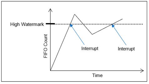
Interrupt Steering and Vector
When interrupts are enabled, the interrupt vector associated with the specific interrupt can be programmed (typically with a unique number/identifier) such that it can be utilized in the Interrupt Service Routine (ISR) to identify the type of interrupt. When an interrupt occurs, the contents of the Interrupt Vector registers is reported as part of the interrupt mechanism. In addition to specifying the interrupt vector, the interrupt can be directed (“steered”) to the native bus or to the application running on the onboard ARM processor.
Note: The Interrupt Vector and Interrupt Steering registers are mapped to the Motherboard Common Memory and these registers are associated with the Module Slot position (refer to Function Register Map).
Interrupt Vector
Function: Set an identifier for the interrupt.
Type: unsigned binary word (32-bit)
Data Range: 0 to 0xFFFF FFFF
Read/Write: R/W
Initialized Value: 0
Operational Settings: When an interrupt occurs, this value is reported as part of the interrupt mechanism.
Interrupt Steering
Function: Set an identifier for the interrupt.
Type: unsigned binary word (32-bit)
Data Range: 0 to 0xFFFF FFFF
Read/Write: R/W
Initialized Value: 0
Operational Settings: When an interrupt occurs, this value is reported as part of the interrupt mechanism.
| Direct Interrupt to VME | 1 |
|---|---|
| Direct Interrupt to ARM Processor (via SerDes) (Custom App on ARM or NAI Ethernet Listener App) | 2 |
| Direct Interrupt to PCIe Bus | 5 |
| Direct Interrupt to cPCI Bus | 6 |
Function Register Map
Key:
Bold Italic = Configuration/Control
Bold Underline = Measurement/Status
*When an event is detected, the bit associated with the event is set in this register and will remain set until the user clears the event bit. Clearing the bit requires writing a 1 back to the specific bit that was set when read (i.e. write-1-to-clear, writing a ‘1’ to a bit set to ‘1’ will set the bit to ‘0’).
**Data is available in Floating Point if Enable Floating Point Mode register is set to Floating Point Mode.
~ Data is always in Floating Point.
D/A Output Registers
| 0x2004 | DAC Value Ch 1**** | R/W |
|---|---|---|
| 0x2104 | DAC Value Ch 2**** | R/W |
| 0x2204 | DAC Value Ch 3**** | R/W |
| 0x2304 | DAC Value Ch 4**** | R/W |
| 0x2404 | DAC Value Ch 5**** | R/W |
| 0x2504 | DAC Value Ch 6**** | R/W |
| 0x2604 | DAC Value Ch 7**** | R/W |
| 0x2704 | DAC Value Ch 8**** | R/W |
D/A Control Registers
| 0x2000 | Voltage Range Ch 1 | R/W |
|---|---|---|
| 0x2100 | Voltage Range Ch 2 | R/W |
| 0x2200 | Voltage Range Ch 3 | R/W |
| 0x2300 | Voltage Range Ch 4 | R/W |
| 0x2400 | Voltage Range Ch 5 | R/W |
| 0x2500 | Voltage Range Ch 6 | R/W |
| 0x2600 | Voltage Range Ch 7 | R/W |
| 0x2700 | Voltage Range Ch 8 | R/W |
| 0x100C | Update Rate Ch 1-8 | R/W |
|---|---|---|
| 0x1010 | Overcurrent Reset Ch 1-8 | R/W |
| 0x1014 | Output Enable Ch 1-8 | R/W |
D/A Measurement Registers
| 0x2008 | Wrap Voltage Ch 1**** | R |
|---|---|---|
| 0x2108 | Wrap Voltage Ch 2**** | R |
| 0x2208 | Wrap Voltage Ch 3**** | R |
| 0x2308 | Wrap Voltage Ch 4**** | R |
| 0x2408 | Wrap Voltage Ch 5**** | R |
| 0x2508 | Wrap Voltage Ch 6**** | R |
| 0x2608 | Wrap Voltage Ch 7**** | R |
| 0x2708 | Wrap Voltage Ch 8**** | R |
| 0x200C | Wrap Current Ch 1**** | R |
|---|---|---|
| 0x210C | Wrap Current Ch 2**** | R |
| 0x220C | Wrap Current Ch 3**** | R |
| 0x230C | Wrap Current Ch 4**** | R |
| 0x240C | Wrap Current Ch 5**** | R |
| 0x250C | Wrap Current Ch 6**** | R |
| 0x260C | Wrap Current Ch 7**** | R |
| 0x270C | Wrap Current Ch 8**** | R |
| 0x2044 | Internal Voltage Ch 1**** | R |
|---|---|---|
| 0x2144 | Internal Voltage Ch 2**** | R |
| 0x2244 | Internal Voltage Ch 3**** | R |
| 0x2344 | Internal Voltage Ch 4**** | R |
| 0x2444 | Internal Voltage Ch 5**** | R |
| 0x2544 | Internal Voltage Ch 6**** | R |
| 0x2644 | Internal Voltage Ch 7**** | R |
| 0x2744 | Internal Voltage Ch 8**** | R |
FIFO Registers
| 0x2008 | FIFO Buffer Data Ch 1**** | R/W |
|---|---|---|
| 0x2118 | FIFO Buffer Data Ch 2**** | R/W |
| 0x2218 | FIFO Buffer Data Ch 3**** | R/W |
| 0x2318 | FIFO Buffer Data Ch 4**** | R/W |
| 0x2418 | FIFO Buffer Data Ch 5**** | R/W |
| 0x2518 | FIFO Buffer Data Ch 6**** | R/W |
| 0x2618 | FIFO Buffer Data Ch 7**** | R/W |
| 0x2718 | FIFO Buffer Data Ch 8**** | R/W |
| 0x201C | FIFO Word Count Ch 1 | R |
|---|---|---|
| 0x211C | FIFO Word Count Ch 2 | R |
| 0x221C | FIFO Word Count Ch 3 | R |
| 0x231C | FIFO Word Count Ch 4 | R |
| 0x241C | FIFO Word Count Ch 5 | R |
| 0x251C | FIFO Word Count Ch 6 | R |
| 0x261C | FIFO Word Count Ch 7 | R |
| 0x271C | FIFO Word Count Ch 8 | R |
| 0x2010 | Clear FIFO Ch 1 | W |
|---|---|---|
| 0x2110 | Clear FIFO Ch 2 | W |
| 0x2210 | Clear FIFO Ch 3 | W |
| 0x2310 | Clear FIFO Ch 4 | W |
| 0x2410 | Clear FIFO Ch 5 | W |
| 0x2510 | Clear FIFO Ch 6 | W |
| 0x2610 | Clear FIFO Ch 7 | W |
| 0x2710 | Clear FIFO Ch 8 | W |
| 0x2014 | FIFO Software Trigger Ch 1 | W |
|---|---|---|
| 0x2114 | FIFO Software Trigger Ch 2 | W |
| 0x2214 | FIFO Software Trigger Ch 3 | W |
| 0x2314 | FIFO Software Trigger Ch 4 | W |
| 0x2414 | FIFO Software Trigger Ch 5 | W |
| 0x2514 | FIFO Software Trigger Ch 6 | W |
| 0x2614 | FIFO Software Trigger Ch 7 | W |
| 0x2714 | FIFO Software Trigger Ch 8 | W |
| 0x1004 | Data Mode Ch 1-8 | R/W |
|---|---|---|
| 0x1008 | Pattern Control Ch 1-8 | R/W |
FIFO Thresholds
| 0x2020 | FIFO Almost Empty Value Ch 1 | R/W |
|---|---|---|
| 0x2120 | FIFO Almost Empty Value Ch 2 | R/W |
| 0x2220 | FIFO Almost Empty Value Ch 3 | R/W |
| 0x2320 | FIFO Almost Empty Value Ch 4 | R/W |
| 0x2420 | FIFO Almost Empty Value Ch 5 | R/W |
| 0x2520 | FIFO Almost Empty Value Ch 6 | R/W |
| 0x2620 | FIFO Almost Empty Value Ch 7 | R/W |
| 0x2720 | FIFO Almost Empty Value Ch 8 | R/W |
| 0x2024 | FIFO Low Watermark Value Ch 1 | R |
|---|---|---|
| 0x2124 | FIFO Low Watermark Value Ch 2 | R |
| 0x2224 | FIFO Low Watermark Value Ch 3 | R |
| 0x2324 | FIFO Low Watermark Value Ch 4 | R |
| 0x2424 | FIFO Low Watermark Value Ch 5 | R |
| 0x2524 | FIFO Low Watermark Value Ch 6 | R |
| 0x2624 | FIFO Low Watermark Value Ch 7 | R |
| 0x2724 | FIFO Low Watermark Value Ch 8 | R |
| 0x2028 | FIFO High Watermark Value Ch 1 | R/W |
|---|---|---|
| 0x2128 | FIFO High Watermark Value Ch 2 | R/W |
| 0x2228 | FIFO High Watermark Value Ch 3 | R/W |
| 0x2328 | FIFO High Watermark Value Ch 4 | R/W |
| 0x2428 | FIFO High Watermark Value Ch 5 | R/W |
| 0x2528 | FIFO High Watermark Value Ch 6 | R/W |
| 0x2628 | FIFO High Watermark Value Ch 7 | R/W |
| 0x2728 | FIFO High Watermark Value Ch 8 | R/W |
| 0x202C | FIFO Almost Full Value Ch 1 | R |
|---|---|---|
| 0x212C | FIFO Almost Full Value Ch 2 | R |
| 0x222C | FIFO Almost Full Value Ch 3 | R |
| 0x232C | FIFO Almost Full Value Ch 4 | R |
| 0x242C | FIFO Almost Full Value Ch 5 | R |
| 0x252C | FIFO Almost Full Value Ch 6 | R |
| 0x262C | FIFO Almost Full Value Ch 7 | R |
| 0x272C | FIFO Almost Full Value Ch 8 | R |
Engineering Scaling Conversion Registers
| 0x02B4 | Enable Floating Point | R/W |
|---|---|---|
| 0x0264 | Floating Point State | R |
| 0x2050 | Floating Point Offset Ch 1~ | R/W |
|---|---|---|
| 0x2150 | Floating Point Offset Ch 2~ | R/W |
| 0x2250 | Floating Point Offset Ch 3~ | R/W |
| 0x2350 | Floating Point Offset Ch 4~ | R/W |
| 0x2450 | Floating Point Offset Ch 5~ | R/W |
| 0x2550 | Floating Point Offset Ch 6~ | R/W |
| 0x2650 | Floating Point Offset Ch 7~ | R/W |
| 0x2750 | Floating Point Offset Ch 8~ | R/W |
| 0x2054 | Floating Point Scale Ch 1~ | R |
|---|---|---|
| 0x2154 | Floating Point Scale Ch 2~ | R |
| 0x2254 | Floating Point Scale Ch 3~ | R |
| 0x2354 | Floating Point Scale Ch 4~ | R |
| 0x2454 | Floating Point Scale Ch 5~ | R |
| 0x2554 | Floating Point Scale Ch 6~ | R |
| 0x2654 | Floating Point Scale Ch 7~ | R |
| 0x2754 | Floating Point Scale Ch 8~ | R |
Module Common Registers
Refer to “Module Common Registers Module Manual” for the Module Common Registers Function Register Map.
D/A Status Registers
| 0x02B0 | Channel Status Enabled | R/W |
|---|
BIT Registers
BIT
| 0x0800 | Dynamic Status | R |
|---|---|---|
| 0x0804 | Latched Status* | R/W |
| 0x0808 | Interrupt Enable | R/W |
| 0x080C | Set Edge/Level Interrupt | R/W |
| 0x0248 | Test Enabled | R/W |
|---|
| 0x02B8 | Background BIT Threshold | R/W |
|---|---|---|
| 0x02BC | BIT Count Clear | W |
| 0x02AC | Power-on BIT Complete++ | R |
|---|
++After power-on, Power-on BIT Complete should be checked before reading the BIT Latched Status.
Status Registers
Overcurrent
| 0x0910 | Dynamic Status | R |
|---|---|---|
| 0x0914 | Latched Status* | R/W |
| 0x0918 | Interrupt Enable | R/W |
| 0x091C | Set Edge/Level Interrupt | R/W |
External Power Under Voltage
| 0x0970 | Dynamic Status | R |
|---|---|---|
| 0x0974 | Latched Status* | R/W |
| 0x0978 | Interrupt Enable | R/W |
| 0x097C | Set Edge/Level Interrupt | R/W |
Inter-FPGA Failure
| 0x09B0 | Dynamic Status | R |
|---|---|---|
| 0x09B4 | Latched Status* | R/W |
| 0x09B8 | Interrupt Enable | R/W |
| 0x09BC | Set Edge/Level Interrupt | R/W |
FIFO
| Ch 1 | ||
| 0x0810 | Dynamic Status | R |
| 0x0814 | Latched Status* | R/W |
| 0x0818 | Interrupt Enable | R/W |
| 0x081C | Set Edge/Level Interrupt | R/W |
| Ch 2 | ||
| 0x0820 | Dynamic Status | R |
| 0x0824 | Latched Status* | R/W |
| 0x0828 | Interrupt Enable | R/W |
| 0x082C | Set Edge/Level Interrupt | R/W |
| Ch 3 | ||
| 0x0830 | Dynamic Status | R |
| 0x0834 | Latched Status* | R/W |
| 0x0838 | Interrupt Enable | R/W |
| 0x083C | Set Edge/Level Interrupt | R/W |
| Ch 4 | ||
| 0x0840 | Dynamic Status | R |
| 0x0844 | Latched Status* | R/W |
| 0x0848 | Interrupt Enable | R/W |
| 0x084C | Set Edge/Level Interrupt | R/W |
| Ch 5 | ||
| 0x0850 | Dynamic Status | R |
| 0x0854 | Latched Status* | R/W |
| 0x0858 | Interrupt Enable | R/W |
| 0x085C | Set Edge/Level Interrupt | R/W |
| Ch 6 | ||
| 0x0860 | Dynamic Status | R |
| 0x0864 | Latched Status* | R/W |
| 0x0868 | Interrupt Enable | R/W |
| 0x086C | Set Edge/Level Interrupt | R/W |
| Ch 7 | ||
| 0x0870 | Dynamic Status | R/W |
| 0x0874 | Latched Status | R/W |
| 0x0878 | Interrupt Enable | R/W |
| 0x087C | Set Edge/Level Interrupt | R/W |
| Ch 8 | ||
| 0x0880 | Dynamic Status | R/W |
| 0x0884 | Latched Status* | R/W |
| 0x0888 | Interrupt Enable | R/W |
| 0x088C | Set Edge/Level Interrupt | R/W |
D/A Interrupt Registers
The Interrupt Vector and Interrupt Steering registers are located on the Motherboard Memory Space and do not require any Module Address Offsets. These registers are accessed using the absolute addresses listed in the table below.
| 0x0500 | Module 1 Interrupt Vector 1 - BIT | R/W |
|---|---|---|
| 0x0504 | Module 1 Interrupt Vector 2 - FIFO Ch 1 | R/W |
| 0x0508 | Module 1 Interrupt Vector 3 - FIFO Ch 2 | R/W |
| 0x050C | Module 1 Interrupt Vector 4 - FIFO Ch 3 | R/W |
| 0x0510 | Module 1 Interrupt Vector 5 - FIFO Ch 4 | R/W |
| 0x0514 | Module 1 Interrupt Vector 6 - FIFO Ch 5 | R/W |
| 0x0518 | Module 1 Interrupt Vector 7 - FIFO Ch 6 | R/W |
| 0x051C | Module 1 Interrupt Vector 8 - FIFO Ch 7 | R/W |
| 0x0520 | Module 1 Interrupt Vector 9 - FIFO Ch 8 | R/W |
| 0x0524 to 0x0540 | Module 1 Interrupt Vector 10-17 - Reserved | R/W |
| 0x0544 | Module 1 Interrupt Vector 18 - Overcurrent | R/W |
| 0x0548 | Module 1 Interrupt Vector 19 - Reserved | R/W |
| 0x054C | Module 1 Interrupt Vector 20 - ExtPwrLoss | R/W |
| 0x0550 to 0x0568 | Module 1 Interrupt Vector 21-27 - Reserved | R/W |
| 0x056C | Module 1 Interrupt Vector 28 - Inter-FPGA | R/W |
| 0x0570 to 0x057C | Module 1 Interrupt Vector 29-32 - Reserved | R/W |
| 0x0600 | Module 1 Interrupt Steering 1 - BIT | R/W |
|---|---|---|
| 0x0604 | Module 1 Interrupt Steering 2 - FIFO Ch 1 | R/W |
| 0x0608 | Module 1 Interrupt Steering 3 - FIFO Ch 2 | R/W |
| 0x060C | Module 1 Interrupt Steering 4 - FIFO Ch 3 | R/W |
| 0x0610 | Module 1 Interrupt Steering 5 - FIFO Ch 4 | R/W |
| 0x0614 | Module 1 Interrupt Steering 6 - FIFO Ch 5 | R/W |
| 0x0618 | Module 1 Interrupt Steering 7 - FIFO Ch 6 | R/W |
| 0x061C | Module 1 Interrupt Steering 8 - FIFO Ch 7 | R/W |
| 0x0620 | Module 1 Interrupt Steering 9 - FIFO Ch 8 | R/W |
| 0x0624 to 0x0640 | Module 1 Interrupt Steering 10-17 - Reserved | R/W |
| 0x0644 | Module 1 Interrupt Steering 18 - Overcurrent | R/W |
| 0x0648 | Module 1 Interrupt Steering 19 - Reserved | R/W |
| 0x064C | Module 1 Interrupt Steering 20 - ExtPwrLoss | R/W |
| 0x0650 to 0x0668 | Module 1 Interrupt Steering 21-27 - Reserved | R/W |
| 0x066C | Module 1 Interrupt Steering 28 - Inter-FPGA | R/W |
| 0x0670 to 0x067C | Module 1 Interrupt Steering 29-32 - Reserved | R/W |
| 0x0700 | Module 2 Interrupt Vector 1 - BIT | R/W |
|---|---|---|
| 0x0704 | Module 2 Interrupt Vector 2 - FIFO Ch 1 | R/W |
| 0x0708 | Module 2 Interrupt Vector 3 - FIFO Ch 2 | R/W |
| 0x070C | Module 2 Interrupt Vector 4 - FIFO Ch 3 | R/W |
| 0x0710 | Module 2 Interrupt Vector 5 - FIFO Ch 4 | R/W |
| 0x0714 | Module 2 Interrupt Vector 6 - FIFO Ch 5 | R/W |
| 0x0718 | Module 2 Interrupt Vector 7 - FIFO Ch 6 | R/W |
| 0x071C | Module 2 Interrupt Vector 8 - FIFO Ch 7 | R/W |
| 0x0720 | Module 2 Interrupt Vector 9 - FIFO Ch 8 | R/W |
| 0x0724 to 0x0740 | Module 2 Interrupt Vector 10-17 - Reserved | R/W |
| 0x0744 | Module 2 Interrupt Vector 18 - Overcurrent | R/W |
| 0x0748 | Module 2 Interrupt Vector 19 - Reserved | R/W |
| 0x074C | Module 2 Interrupt Vector 20 - ExtPwrLoss | R/W |
| 0x0754 | Module 2 Interrupt Vector 22 - Reserved | R/W |
| 0x0758 | Module 2 Interrupt Vector 23 - Saturation | R/W |
| 0x075C to 0x0768 | Module 2 Interrupt Vector 24-27 - Reserved | R/W |
| 0x076C | Module 2 Interrupt Vector 28 - Inter-FPGA | R/W |
| 0x0770 to 0x077C | Module 2 Interrupt Vector 29-32 - Reserved | R/W |
| 0x0800 | Module 2 Interrupt Steering 1 - BIT | R/W |
|---|---|---|
| 0x0804 | Module 2 Interrupt Steering 2 - FIFO Ch 1 | R/W |
| 0x0808 | Module 2 Interrupt Steering 3 - FIFO Ch 2 | R/W |
| 0x080C | Module 2 Interrupt Steering 4 - FIFO Ch 3 | R/W |
| 0x0810 | Module 2 Interrupt Steering 5 - FIFO Ch 4 | R/W |
| 0x0814 | Module 2 Interrupt Steering 6 - FIFO Ch 5 | R/W |
| 0x0818 | Module 2 Interrupt Steering 7 - FIFO Ch 6 | R/W |
| 0x081C | Module 2 Interrupt Steering 8 - FIFO Ch 7 | R/W |
| 0x0820 | Module 2 Interrupt Steering 9 - FIFO Ch 8 | R/W |
| 0x0824 to 0x0840 | Module 2 Interrupt Steering 10-17 - Reserved | R/W |
| 0x0844 | Module 2 Interrupt Steering 18 - Overcurrent | R/W |
| 0x0848 | Module 2 Interrupt Steering 19 - Reserved | R/W |
| 0x084C | Module 2 Interrupt Steering 20 - ExtPwrLoss | R/W |
| 0x085C to 0x0868 | Module 2 Interrupt Steering 21-27 - Reserved | R/W |
| 0x086C | Module 2 Interrupt Steering 28 - Inter-FPGA | R/W |
| 0x0870 to 0x087C | Module 2 Interrupt Steering 29-32 - Reserved | R/W |
| 0x0900 | Module 3 Interrupt Vector 1 - BIT | R/W |
|---|---|---|
| 0x0904 | Module 3 Interrupt Vector 2 - FIFO Ch 1 | R/W |
| 0x0908 | Module 3 Interrupt Vector 3 - FIFO Ch 2 | R/W |
| 0x090C | Module 3 Interrupt Vector 4 - FIFO Ch 3 | R/W |
| 0x0910 | Module 3 Interrupt Vector 5 - FIFO Ch 4 | R/W |
| 0x0914 | Module 3 Interrupt Vector 6 - FIFO Ch 5 | R/W |
| 0x0918 | Module 3 Interrupt Vector 7 - FIFO Ch 6 | R/W |
| 0x091C | Module 3 Interrupt Vector 8 - FIFO Ch 7 | R/W |
| 0x0920 | Module 3 Interrupt Vector 9 - FIFO Ch 8 | R/W |
| 0x0924 to 0x0940 | Module 3 Interrupt Vector 10-17 - Reserved | R/W |
| 0x0944 | Module 3 Interrupt Vector 18 - Overcurrent | R/W |
| 0x0948 | Module 3 Interrupt Vector 19 - Reserved | R/W |
| 0x094C | Module 3 Interrupt Vector 20 - ExtPwrLoss | R/W |
| 0x095C to 0x0968 | Module 3 Interrupt Vector 21-27 - Reserved | R/W |
| 0x096C | Module 3 Interrupt Vector 28 - Inter-FPGA | R/W |
| 0x0970 to 0x097C | Module 3 Interrupt Vector 29-32 - Reserved | R/W |
| 0x0A00 | Module 3 Interrupt Steering 1 - BIT | R/W |
|---|---|---|
| 0x0A04 | Module 3 Interrupt Steering 2 - FIFO Ch 1 | R/W |
| 0x0A08 | Module 3 Interrupt Steering 3 - FIFO Ch 2 | R/W |
| 0x0A0C | Module 3 Interrupt Steering 4 - FIFO Ch 3 | R/W |
| 0x0A10 | Module 3 Interrupt Steering 5 - FIFO Ch 4 | R/W |
| 0x0A14 | Module 3 Interrupt Steering 6 - FIFO Ch 5 | R/W |
| 0x0A18 | Module 3 Interrupt Steering 7 - FIFO Ch 6 | R/W |
| 0x0A1C | Module 3 Interrupt Steering 8 - FIFO Ch 7 | R/W |
| 0x0A20 | Module 3 Interrupt Steering 9 - FIFO Ch 8 | R/W |
| 0x0A24 to 0x0A40 | Module 3 Interrupt Steering 10-17 - Reserved | R/W |
| 0x0A44 | Module 3 Interrupt Steering 18 - Overcurrent | R/W |
| 0x0A48 | Module 3 Interrupt Steering 19 - Reserved | R/W |
| 0x0A4C | Module 3 Interrupt Steering 20 - ExtPwrLoss | R/W |
| 0x0A5C to 0x0A68 | Module 3 Interrupt Steering 21-27 - Reserved | R/W |
| 0x086C | Module 3 Interrupt Steering 28 - Inter-FPGA | R/W |
| 0x0870 to 0x087C | Module 3 Interrupt Steering 29-32 - Reserved | R/W |
| 0x0B00 | Module 4 Interrupt Vector 1 - BIT | R/W |
|---|---|---|
| 0x0B04 | Module 4 Interrupt Vector 2 - FIFO Ch 1 | R/W |
| 0x0B08 | Module 4 Interrupt Vector 3 - FIFO Ch 2 | R/W |
| 0x0B0C | Module 4 Interrupt Vector 4 - FIFO Ch 3 | R/W |
| 0x0B10 | Module 4 Interrupt Vector 5 - FIFO Ch 4 | R/W |
| 0x0B14 | Module 4 Interrupt Vector 6 - FIFO Ch 5 | R/W |
| 0x0B18 | Module 4 Interrupt Vector 7 - FIFO Ch 6 | R/W |
| 0x0B1C | Module 4 Interrupt Vector 8 - FIFO Ch 7 | R/W |
| 0x0B20 | Module 4 Interrupt Vector 9 - FIFO Ch 8 | R/W |
| 0x0B24 to 0x0B40 | Module 4 Interrupt Vector 10-17 - Reserved | R/W |
| 0x0B44 | Module 4 Interrupt Vector 18 - Overcurrent | R/W |
| 0x0B48 | Module 4 Interrupt Vector 19 - Reserved | R/W |
| 0x0B4C | Module 4 Interrupt Vector 20 - ExtPwrLoss | R/W |
| 0x0B5C to 0x0B68 | Module 4 Interrupt Vector 21-27 - Reserved | R/W |
| 0x0B6C | Module 4 Interrupt Vector 28 - Inter-FPGA | R/W |
| 0x0B70 to 0x0B7C | Module 4 Interrupt Vector 29-32 - Reserved | R/W |
| 0x0C00 | Module 4 Interrupt Steering 1 - BIT | R/W |
|---|---|---|
| 0x0C04 | Module 4 Interrupt Steering 2 - FIFO Ch 1 | R/W |
| 0x0C08 | Module 4 Interrupt Steering 3 - FIFO Ch 2 | R/W |
| 0x0C0C | Module 4 Interrupt Steering 4 - FIFO Ch 3 | R/W |
| 0x0C10 | Module 4 Interrupt Steering 5 - FIFO Ch 4 | R/W |
| 0x0C14 | Module 4 Interrupt Steering 6 - FIFO Ch 5 | R/W |
| 0x0C18 | Module 4 Interrupt Steering 7 - FIFO Ch 6 | R/W |
| 0x0C1C | Module 4 Interrupt Steering 8 - FIFO Ch 7 | R/W |
| 0x0C20 | Module 4 Interrupt Steering 9 - FIFO Ch 8 | R/W |
| 0x0C24 to 0x0C44 | Module 4 Interrupt Steering 10-18 - Reserved | R/W |
| 0x0C44 | Module 4 Interrupt Steering 18 - Overcurrent | R/W |
| 0x0C48 | Module 4 Interrupt Steering 19 - Reserved | R/W |
| 0x0C4C | Module 4 Interrupt Steering 20 - ExtPwrLoss | R/W |
| 0x0C5C to 0x0C68 | Module 4 Interrupt Steering 21-27 - Reserved | R/W |
| 0x0C6C | Module 4 Interrupt Steering 28 - Inter-FPGA | R/W |
| 0x0C70 to 0x0C7C | Module 4 Interrupt Steering 29-32 - Reserved | R/W |
| 0x0D00 | Module 5 Interrupt Vector 1 - BIT | R/W |
|---|---|---|
| 0x0D04 | Module 5 Interrupt Vector 2 - FIFO Ch 1 | R/W |
| 0x0D08 | Module 5 Interrupt Vector 3 - FIFO Ch 2 | R/W |
| 0x0D0C | Module 5 Interrupt Vector 4 - FIFO Ch 3 | R/W |
| 0x0D10 | Module 5 Interrupt Vector 5 - FIFO Ch 4 | R/W |
| 0x0D14 | Module 5 Interrupt Vector 6 - FIFO Ch 5 | R/W |
| 0x0D18 | Module 5 Interrupt Vector 7 - FIFO Ch 6 | R/W |
| 0x0D1C | Module 5 Interrupt Vector 8 - FIFO Ch 7 | R/W |
| 0x0D20 | Module 5 Interrupt Vector 9 - FIFO Ch 8 | R/W |
| 0x0D24 to 0x0D40 | Module 5 Interrupt Vector 10-17 - Reserved | R/W |
| 0x0D44 | Module 5 Interrupt Vector 18 - Overcurrent | R/W |
| 0x0D48 | Module 5 Interrupt Vector 19 - Reserved | R/W |
| 0x0D4C | Module 5 Interrupt Vector 20 - ExtPwrLoss | R/W |
| 0x0D5C to 0x0D68 | Module 5 Interrupt Vector 21-27 - Reserved | R/W |
| 0x0D6C | Module 5 Interrupt Vector 28 - Inter-FPGA | R/W |
| 0x0D70 to 0x0D7C | Module 5 Interrupt Vector 29-32 - Reserved | R/W |
| 0x0E00 | Module 5 Interrupt Steering 1 - BIT | R/W |
|---|---|---|
| 0x0E04 | Module 5 Interrupt Steering 2 - FIFO Ch 1 | R/W |
| 0x0E08 | Module 5 Interrupt Steering 3 - FIFO Ch 2 | R/W |
| 0x0E0C | Module 5 Interrupt Steering 4 - FIFO Ch 3 | R/W |
| 0x0E10 | Module 5 Interrupt Steering 5 - FIFO Ch 4 | R/W |
| 0x0E14 | Module 5 Interrupt Steering 6 - FIFO Ch 5 | R/W |
| 0x0E18 | Module 5 Interrupt Steering 7 - FIFO Ch 6 | R/W |
| 0x0E1C | Module 5 Interrupt Steering 8 - FIFO Ch 7 | R/W |
| 0x0E20 | Module 5 Interrupt Steering 9 - FIFO Ch 8 | R/W |
| 0x0E24 to 0x0E40 | Module 5 Interrupt Steering 10-17 - Reserved | R/W |
| 0x0E44 | Module 5 Interrupt Steering 18 - Overcurrent | R/W |
| 0x0E48 | Module 5 Interrupt Steering 19 - Reserved | R/W |
| 0x0E4C | Module 5 Interrupt Steering 20 - ExtPwrLoss | R/W |
| 0x0E5C to 0x0E68 | Module 5 Interrupt Steering 21-27 - Reserved | R/W |
| 0x0E6C | Module 5 Interrupt Steering 28 - Inter-FPGA | R/W |
| 0x0E70 to 0x0E7C | Module 5 Interrupt Steering 29-32 - Reserved | R/W |
| 0x0F00 | Module 6 Interrupt Vector 1 - BIT | R/W |
|---|---|---|
| 0x0F04 | Module 6 Interrupt Vector 2 - FIFO Ch 1 | R/W |
| 0x0F08 | Module 6 Interrupt Vector 3 - FIFO Ch 2 | R/W |
| 0x0F0C | Module 6 Interrupt Vector 4 - FIFO Ch 3 | R/W |
| 0x0F10 | Module 6 Interrupt Vector 5 - FIFO Ch 4 | R/W |
| 0x0F14 | Module 6 Interrupt Vector 6 - FIFO Ch 5 | R/W |
| 0x0F18 | Module 6 Interrupt Vector 7 - FIFO Ch 6 | R/W |
| 0x0F1C | Module 6 Interrupt Vector 8 - FIFO Ch 7 | R/W |
| 0x0F20 | Module 6 Interrupt Vector 9 - FIFO Ch 8 | R/W |
| 0x0F24 to 0x0F40 | Module 6 Interrupt Vector 10-17 - Reserved | R/W |
| 0x0F44 | Module 6 Interrupt Vector 18 - Overcurrent | R/W |
| 0x0F48 | Module 6 Interrupt Vector 19 - Reserved | R/W |
| 0x0F4C | Module 6 Interrupt Vector 20 - ExtPwrLoss | R/W |
| 0x0F5C to 0x0F68 | Module 6 Interrupt Vector 21-27 - Reserved | R/W |
| 0x0F6C | Module 6 Interrupt Vector 28 - Inter-FPGA | R/W |
| 0x0F70 to 0x0F7C | Module 6 Interrupt Vector 29-32 - Reserved | R/W |
| 0x1000 | Module 6 Interrupt Steering 1 - BIT | R/W |
|---|---|---|
| 0x1004 | Module 6 Interrupt Steering 2 - FIFO Ch 1 | R/W |
| 0x0E08 | Module 6 Interrupt Steering 3 - FIFO Ch 2 | R/W |
| 0x100C | Module 6 Interrupt Steering 4 - FIFO Ch 3 | R/W |
| 0x1010 | Module 6 Interrupt Steering 5 - FIFO Ch 4 | R/W |
| 0x1014 | Module 6 Interrupt Steering 6 - FIFO Ch 5 | R/W |
| 0x1018 | Module 6 Interrupt Steering 7 - FIFO Ch 6 | R/W |
| 0x101C | Module 6 Interrupt Steering 8 - FIFO Ch 7 | R/W |
| 0x1020 | Module 6 Interrupt Steering 9 - FIFO Ch 8 | R/W |
| 0x1024 to 0x1040 | Module 6 Interrupt Steering 10-17 - Reserved | R/W |
| 0x1044 | Module 6 Interrupt Steering 18 - Overcurrent | R/W |
| 0x1048 | Module 6 Interrupt Steering 19 - Reserved | R/W |
| 0x104C | Module 6 Interrupt Steering 20 - ExtPwrLoss | R/W |
| 0x105C to 0x1068 | Module 6 Interrupt Steering 21-27 - Reserved | R/W |
| 0x106C | Module 6 Interrupt Steering 28 - Inter-FPGA | R/W |
| 0x1070 to 0x107C | Module 6 Interrupt Steering 29-32 - Reserved | R/W |
Appendix B: Integer/Floating Point Mode Programming
Integer Mode Programming
The following registers should be configured as follows:
| Register | Value | Description |
|---|---|---|
| Voltage Range | 0x4 | ±10 volts |
| Enable Floating Point | 0 | Disable for Floating Point Mode |
Note: LSB for Bipolar ±10-volt range:
LSB = 10/0x00007FFF = 10/32767=305uV
| DAC Value (Integer) | DAC Voltage Output |
|---|---|
| .000 of FS = 0x0000 7FFF | 32767 * LSB = 10.0 volts |
| 0.5 of FS = 0x0000 4000 | 16384 * LSB = 5.0 volts |
| 0.0 of FS = 0x0000 0000 | 0 * LSB = 0.0 volts |
| -0.5 of FS = 0xFFFF C000 | -16384 * LSB = -5.0 volts |
| -1.0 of FS = 0xFFFF 8000 | -32768 * LSB = -10. volts |
Floating Point Mode Voltage Programming
The following registers should be configured as follows:
| Register | Value | Description |
|---|---|---|
| Voltage Range | 0x4 | ±10 volts |
| Enable Floating Point | 1 | Enable for Floating Point Mode |
| Floating Point Scale | 0.1 | Scale = 1 / (Full Range) # 1 / 10.0 = 0.1 |
| Floating Point Offset | 0.0 | No Offset |
Note: LSB for Bipolar ±10-volt range:
LSB = 10/0x00007FFF
10/32767=305uV
| DAC Value (volts) (Floating Point) | DAC Value (Calculated by Module) | DAC Value (Integer) | DAC Voltage Output |
|---|---|---|---|
| 10.0 | (10.0 + 0.0) **0.1 = 1 (FS) | FS = 0x0000 7FFF | 32767 ** LSB = 10.0 volts |
| 5.0 | (5.0 + 0.0) **0.1 = 0.5 of FS | 0.5 of FS = 0x0000 4000 | 16384 ** LSB = 5.0 volts |
| 0.0 | (0.0 + 0.0) **0.1 = 0.0 of FS | 0.0 of FS = 0x0000 0000 | 0 ** LSB = 0.0 volts |
| -5.0 | (-5.0 + 0.0) **0.1 = -0.5 of FS | -0.5 of FS = 0xFFFF C000 | -16384 ** LSB = -5.0 volts |
| -10.0 | (-10.0 + 0.0) **0.1 = -1 (-FS) | -FS = 0xFFFF 8000 | -32768 ** LSB = -10. volts |
Floating Point Mode Engineering Units Programming
Example #1:
An application wants to associate -10 to 10 volts to -5 to 5 inches.
The following registers should be configured as follows:
| Register | Value | Description |
|---|---|---|
| Voltage Range | 0x4 ±10 volts | Enable Floating Point |
| 1 | Enable for Floating Point Mode | Floating Point Scale |
| 0.2 | Scale = 1 / inches range # 1 / 5 = 0.2 | Floating Point Offset |
| 0.0 | No Offset |
Note: LSB for Bipolar ±10-volt range:
LSB = 10/0x00007FFF
10/32767=305uV
| DAC Value (volts) (Floating Point) | DAC Value (Calculated by Module) | DAC Value (Integer) | DAC Voltage Output |
|---|---|---|---|
| 5.0 | (5.0 + 0.0) * 0.2 = 1 (FS) | FS = 0x0000 7FFF | 32767 * LSB = 10.0 volts |
| 2.5 | (2.5 + 0.0) * 0.2 = .5 of FS | 0.5 of FS = 0x0000 4000 | 16384 * LSB = 5.0 volts |
| 0.0 | (0.0 + 0.0) * 0.2 = 0 | 0.0 of FS = 0x0000 0000 | 0 * LSB = 0.0 volts |
| -2.5 | (-2.5 + 0.0) * 0.2 = -.5 of FS | -0.5 of FS = 0xFFFF C000 | -16384 * LSB = -5.0 volts |
| -5.0 | (-5.0 + 0.0) * 0.2 = -1 (-FS) | -FS = 0xFFFF 8000 | -32768 * LSB = -10. volts |
Example #2:
An application wants to associate 0 to 10 volts to 0 to 50 feet with a bias of 0.5 feet (in other words 0.5 feet is equivalent to 0 volts).
The following registers should be configured as follows:
| Register | Value | Description |
|---|---|---|
| Voltage Range | 0x1 | Unipolar 0-10 volts |
| Enable Floating Point | 1 | Enable for Floating Point Mode |
| Floating Point Scale | 0.02 | Scale = 1 / feet range # 1 / 50 = 0.02 |
| Floating Point Offset | -0.50 | Bias (0.5 feet) that is equivalent to 0 volts |
The following are sample outputs:
Note: LSB for Unipolar 10-volt range:
LSB = 10/0x0000FFFF
10/65535
| DAC Value (volts) (Floating Point) | DAC Value (Calculated by Module) | DAC Value (Integer) | DAC Voltage Output |
|---|---|---|---|
| 50.00 | (50.0 - 0.50) * 0.02 = 0.99 of FS | 0.99 of FS = 0x0000 FD70 | 64880 * LSB = 9.90 volts |
| 25.00 | (25.00 - 0.50) * 0.02 = 0.49 of FS | 0.49 of FS = 0x0000 7D70 | 32112 * LSB = 4.90 volts |
| 5.50 | (5.50 - 0.50) * 0.02 = 0.10 of FS | 0.10 of FS = 0x0000 199A | 6554 * LSB = 1.00 volts |
| 0.50 | (0.50 - 0.50) * 0.02 = 0.00 of FS | 0.00 of FS = 0x0000 0000 | 0 * LSB = 0.0 volts |
PIN-OUT DETAILS
Pin-out details (for reference) are shown below, with respect to DATAIO. Additional information on pin-outs can be found in the Motherboard Operational Manuals.
| Module Signal (Ref Only) | 44-Pin I/O | 50-Pin I/O (Mod Slot 1-J3) | 50-Pin I/O (Mod Slot 2-J4) | 50-Pin I/O (Mod Slot 3-J3) | 50-Pin I/O (Mod Slot 3-J4) | 8 CH D/A (DA2) & 8 CH A/D (ADE) (CME) | 8 CH D/A (DA2) & 8 CH A/D (ADF) (CMF) |
|---|---|---|---|---|---|---|---|
| DATIO1 | 2 | 10 | 1 | 2 | IN_CH01+ | IN_CH01+ | |
| DATIO2 | 24 | 35 | 26 | 27 | IN_CH01- | IN_CH01- | |
| DATIO3 | 3 | 11 | 2 | 3 | IN_CH02+ | IN_CH02+ | |
| DATIO4 | 25 | 36 | 27 | 28 | IN_CH02- | IN_CH02- | |
| DATIO5 | 5 | 13 | 4 | 5 | IN_CH04+ | IN_CH04+ | |
| DATIO6 | 27 | 38 | 29 | 30 | IN_CH04- | IN_CH04- | |
| DATIO7 | 7 | 14 | 5 | 6 | IN_CH05+ | IN_CH05+ | |
| DATIO8 | 29 | 39 | 30 | 31 | IN_CH05- | IN_CH05- | |
| DATIO9 | 8 | 15 | 6 | 7 | IN_CH06+ | IN_CH06+ | |
| DATIO10 | 30 | 40 | 31 | 32 | IN_CH06- | IN_CH06- | |
| DATIO11 | 10 | 17 | 8 | 9 | IN_CH08+ | IN_CH08+ | |
| DATIO12 | 32 | 42 | 33 | 34 | IN_CH08-(GND-CMRP) | IN_CH08- | |
| DATIO13 | 12 | 42 | 33 | 34 | OUT_CH1 | OUT_CH1 | |
| DATIO14 | 34 | 43 | 34 | 42 | OUT_CH2 | OUT_CH2 | |
| DATIO15 | 13 | 19 | 10 | 18 | OUT_CH3 | OUT_CH3 | |
| DATIO16 | 35 | 44 | 35 | 43 | OUT_CH4 | OUT_CH4 | |
| DATIO17 | 15 | 21 | 12 | 20 | GND-DA | GND-DA | |
| DATIO18 | 37 | 46 | 37 | 45 | GND-DA | GND-DA | |
| DATIO19 | 17 | 22 | 13 | 21 | OUT_CH5 | OUT_CH5 | |
| DATIO20 | 39 | 47 | 38 | 46 | OUT_CH6 | OUT_CH6 | |
| DATIO21 | 18 | 23 | 14 | 22 | OUT_CH7 | OUT_CH7 | |
| DATIO22 | 40 | 48 | 39 | 47 | OUT_CH8 | OUT_CH8 | |
| DATIO23 | 20 | 25 | 16 | 24 | GND-DA | GND-DA | |
| DATIO24 | 42 | 50 | 41 | 49 | GND-DA | GND-DA | |
| DATIO25 | 4 | 50 | 41 | 49 | IN_CH03+ | IN_CH03+ | |
| DATIO26 | 26 | 37 | 28 | 29 | IN_CH03- | IN_CH03- | |
| DATIO27 | 9 | 16 | 7 | 8 | IN_CH07+ | IN_CH07+ | |
| DATIO28 | 31 | 41 | 32 | 33 | IN_CH07- | IN_CH07- | |
| DATIO29 | 14 | 20 | 11 | 19 | |||
| DATIO30 | 36 | 45 | 36 | 44 | |||
| DATIO31 | 19 | 24 | 15 | 23 | GND-DA | GND-DA | |
| DATIO32 | 41 | 49 | 40 | 48 | GND-DA | GND-DA | |
| DATIO33 | 6 | EXT-SYNC+ | EXT-SYNC+ | ||||
| DATIO34 | 28 | EXT-SYNC- | EXT-SYNC- | ||||
| DATIO35 | 11 | ||||||
| DATIO36 | 33 | ||||||
| DATIO37 | 16 | ||||||
| DATIO38 | 38 | ||||||
| DATIO39 | 21 | ||||||
| DATIO40 | 43 | ||||||
| N/A |
STATUS AND INTERRUPTS
Status registers indicate the detection of faults or events. The status registers can be channel bit-mapped or event bit-mapped. An example of a channel bit-mapped register is the BIT status register, and an example of an event bit-mapped register is the FIFO status register.
For those status registers that allow interrupts to be generated upon the detection of the fault or the event, there are four registers associated with each status: Dynamic, Latched, Interrupt Enabled, and Set Edge/Level Interrupt.
Dynamic Status: The Dynamic Status register indicates the current condition of the fault or the event. If the fault or the event is momentary, the contents in this register will be clear when the fault or the event goes away. The Dynamic Status register can be polled, however, if the fault or the event is sporadic, it is possible for the indication of the fault or the event to be missed.
Latched Status: The Latched Status register indicates whether the fault or the event has occurred and keeps the state until it is cleared by the user. Reading the Latched Status register is a better alternative to polling the Dynamic Status register because the contents of this register will not clear until the user commands to clear the specific bit(s) associated with the fault or the event in the Latched Status register. Once the status register has been read, the act of writing a 1 back to the applicable status register to any specific bit (channel/event) location will “clear” the bit (set the bit to 0). When clearing the channel/event bits, it is strongly recommended to write back the same bit pattern as read from the Latched Status register. For example, if the channel bit-mapped Latched Status register contains the value 0x0000 0005, which indicates fault/event detection on channel 1 and 3, write the value 0x0000 0005 to the Latched Status register to clear the fault/event status for channel 1 and 3. Writing a “1” to other channels that are not set (example 0x0000 000F) may result in incorrectly “clearing” incoming faults/events for those channels (example, channel 2 and 4).
Interrupt Enable: If interrupts are preferred upon the detection of a fault or an event, enable the specific channel/event interrupt in the Interrupt Enable register. The bits in Interrupt Enable register map to the same bits in the Latched Status register. When a fault or event occurs, an interrupt will be fired. Subsequent interrupts will not trigger until the application acknowledges the fired interrupt by clearing the associated channel/event bit in the Latched Status register. If the interruptible condition is still persistent after clearing the bit, this may retrigger the interrupt depending on the Edge/Level setting.
Set Edge/Level Interrupt: When interrupts are enabled, the condition on retriggering the interrupt after the Latch Register is “cleared” can be specified as “edge” triggered or “level” triggered. Note, the Edge/Level Trigger also affects how the Latched Register value is adjusted after it is “cleared” (see below).
Edge triggered: An interrupt will be retriggered when the Latched Status register change from low (0) to high (1) state. Uses for edge-triggered interrupts would include transition detections (Low-to-High transitions, High-to-Low transitions) or fault detections. After “clearing” an interrupt, another interrupt will not occur until the next transition or the re-occurrence of the fault again.
Level triggered: An interrupt will be generated when the Latched Status register remains at the high (1) state. Level-triggered interrupts are used to indicate that something needs attention.
Interrupt Vector and Steering
When interrupts are enabled, the interrupt vector associated with the specific interrupt can be programmed with a unique number/identifier defined by the user such that it can be utilized in the Interrupt Service Routine (ISR) to identify the type of interrupt. When an interrupt occurs, the contents of the Interrupt Vector registers is reported as part of the interrupt mechanism. In addition to specifying the interrupt vector, the interrupt can be directed (“steered”) to the native bus or to the application running on the onboard ARM processor.
Interrupt Trigger Types
In most applications, limiting the number of interrupts generated is preferred as interrupts are costly, thus choosing the correct Edge/Level interrupt trigger to use is important.
Example 1: Fault detection
This example illustrates interrupt considerations when detecting a fault like an “open” on a line. When an “open” is detected, the system will receive an interrupt. If the “open” on the line is persistent and the trigger is set to “edge”, upon “clearing” the interrupt, the system will not regenerate another interrupt. If, instead, the trigger is set to “level”, upon “clearing” the interrupt, the system will re-generate another interrupt. Thus, in this case, it will be better to set the trigger type to “edge”.
Example 2: Threshold detection
This example illustrates interrupt considerations when detecting an event like reaching or exceeding the “high watermark” threshold value. In a communication device, when the number of elements received in the FIFO reaches the high-watermark threshold, an interrupt will be generated. Normally, the application would read the count of the number of elements in the FIFO and read this number of elements from the FIFO. After reading the FIFO data, the application would “clear” the interrupt. If the trigger type is set to “edge”, another interrupt will be generated only if the number of elements in FIFO goes below the “high watermark” after the “clearing” the interrupt and then fills up to reach the “high watermark” threshold value. Since receiving communication data is inherently asynchronous, it is possible that data can continue to fill the FIFO as the application is pulling data off the FIFO. If, at the time the interrupt is “cleared”, the number of elements in the FIFO is at or above the “high watermark”, no interrupts will be generated. In this case, it will be better to set the trigger type to “level”, as the purpose here is to make sure that the FIFO is serviced when the number of elements exceeds the high watermark threshold value. Thus, upon “clearing” the interrupt, if the number of elements in the FIFO is at or above the “high watermark” threshold value, another interrupt will be generated indicating that the FIFO needs to be serviced.
Dynamic and Latched Status Registers Examples
The examples in this section illustrate the differences in behavior of the Dynamic Status and Latched Status registers as well as the differences in behavior of Edge/Level Trigger when the Latched Status register is cleared.
Figure 1. Example of Module's Channel-Mapped Dynamic and Latched Status States
No Clearing of
Latched StatusClearing of Latched Status
(Edge-Triggered)Clearing of Latched Status
(Level-Triggered)Time Dynamic Status Latched Status Action Latched Status Action Latched T0 0x0 0x0 Read Latched Register 0x0 Read Latched Register 0x0 T1 0x1 0x1 Read Latched Register 0x1 0x1 T1 0x1 0x1 Write 0x1 to Latched Register Write 0x1 to Latched Register T1 0x1 0x1 0x0 0x1 T2 0x0 0x1 Read Latched Register 0x0 Read Latched Register 0x1 T2 0x0 0x1 Read Latched Register 0x0 Write 0x1 to Latched Register T2 0x0 0x1 Read Latched Register 0x0 0x0 T3 0x2 0x3 Read Latched Register 0x2 Read Latched Register 0x2 T3 0x2 0x3 Write 0x2 to Latched Register Write 0x2 to Latched Register T3 0x2 0x3 0x0 0x2 T4 0x2 0x3 Read Latched Register 0x1 Read Latched Register 0x3 T4 0x2 0x3 Write 0x1 to Latched Register Write 0x3 to Latched Register T4 0x2 0x3 0x0 0x2 T5 0xC 0xF Read Latched Register 0xC Read Latched Register 0xE T5 0xC 0xF Write 0xC to Latched Register Write 0xE to Latched Register T5 0xC 0xF 0x0 0xC T6 0xC 0xF Read Latched Register 0x0 Read Latched 0xC T6 0xC 0xF Read Latched Register 0x0 Write 0xC to Latched Register T6 0xC 0xF Read Latched Register 0x0 0xC T7 0x4 0xF Read Latched Register 0x0 Read Latched Register 0xC T7 0x4 0xF Read Latched Register 0x0 Write 0xC to Latched Register T7 0x4 0xF Read Latched Register 0x0 0x4 T8 0x4 0xF Read Latched Register 0x0 Read Latched Register 0x4 Interrupt Examples
The examples in this section illustrate the interrupt behavior with Edge/Level Trigger.
Figure 2. Illustration of Latched Status State for Module with 4-Channels with Interrupt Enabled
Time Latched Status
(Edge-Triggered -
Clear Multi-Channel)Latched Status
(Edge-Triggered -
Clear Single Channel)Latched Status
(Level-Triggered -
Clear Multi-Channel)Action Latched Action Latched Action Latched T1
(Int 1)Interrupt Generated
Read Latched Registers0x1 Interrupt Generated
Read Latched Registers0x1 Interrupt Generated
Read Latched Registers0x1 T1
(Int 1)Write 0x1 to Latched Register Write 0x1 to Latched Register Write 0x1 to Latched Register T1
(Int 1)0x0 0x0 Interrupt re-triggers
Note, interrupt re-triggers after
each clear until T2.0x1 T3
(Int 2)Interrupt Generated
Read Latched Registers0x2 Interrupt Generated
Read Latched Registers0x2 Interrupt Generated
Read Latched Registers0x2 T3
(Int 2)Write 0x2 to Latched Register Write 0x2 to Latched Register Write 0x2 to Latched Register T3
(Int 2)0x0 0x0 Interrupt re-triggers
Note, interrupt re-triggers after
each clear until T7.0x2 T4
(Int 3)Interrupt Generated
Read Latched Registers0x1 Interrupt Generated
Read Latched Registers0x1 Interrupt Generated
Read Latched Registers0x3 T4
(Int 3)Write 0x1 to Latched Register Write 0x1 to Latched Register Write 0x3 to Latched Register T4
(Int 3)0x0 0x0 Interrupt re-triggers
Note, interrupt re-triggers after
each clear and 0x3 is reported
in Latched Register until T5.0x3 T4
(Int 3)0x0 0x0 Interrupt re-triggers
Note, interrupt re-triggers after
each clear until T7.0x2 T6
(Int 4)Interrupt Generated
Read Latched Registers0xC Interrupt Generated
Read Latched Registers0xC Interrupt Generated
Read Latched Registers0xE T6
(Int 4)Write 0xC to Latched Register Write 0x4 to Latched Register Write 0xE to Latched Register T6
(Int 4)0x0 Interrupt re-triggers
Write 0x8 to Latched Register0x8 Interrupt re-triggers
Note, interrupt re-triggers after
each clear and 0xE is
reported in Latched Register until T7.0xE T6
(Int 4)0x0 0x0 Interrupt re-triggers
Note, interrupt re-triggers after
each clear and 0xC is
reported in Latched Register until T8.0xC T6
(Int 4)0x0 0x0 Interrupt re-triggers
Note, interrupt re-triggers after
each clear and 0x4 is
reported in Latched Register always.0x4 REVISION HISTORY
Motherboard Manual - Status and Interrupts Revision History Revision Revision Date Description C 2021-11-30 C08896; Transition manual to docbuilder format - no technical info change. Link to original
DOCS.NAII REVISIONS Revision Date Description 2026-03-02 Formatting updates to document; no technical changes. 2026-05-18 Fixed formatting issues from conversion to new doc site format. 2026-05-19 Fixed minor formatting issue with Interrupt Examples table structure (removed extraneous cell). 2026-07-15 Revised image files for image quality.
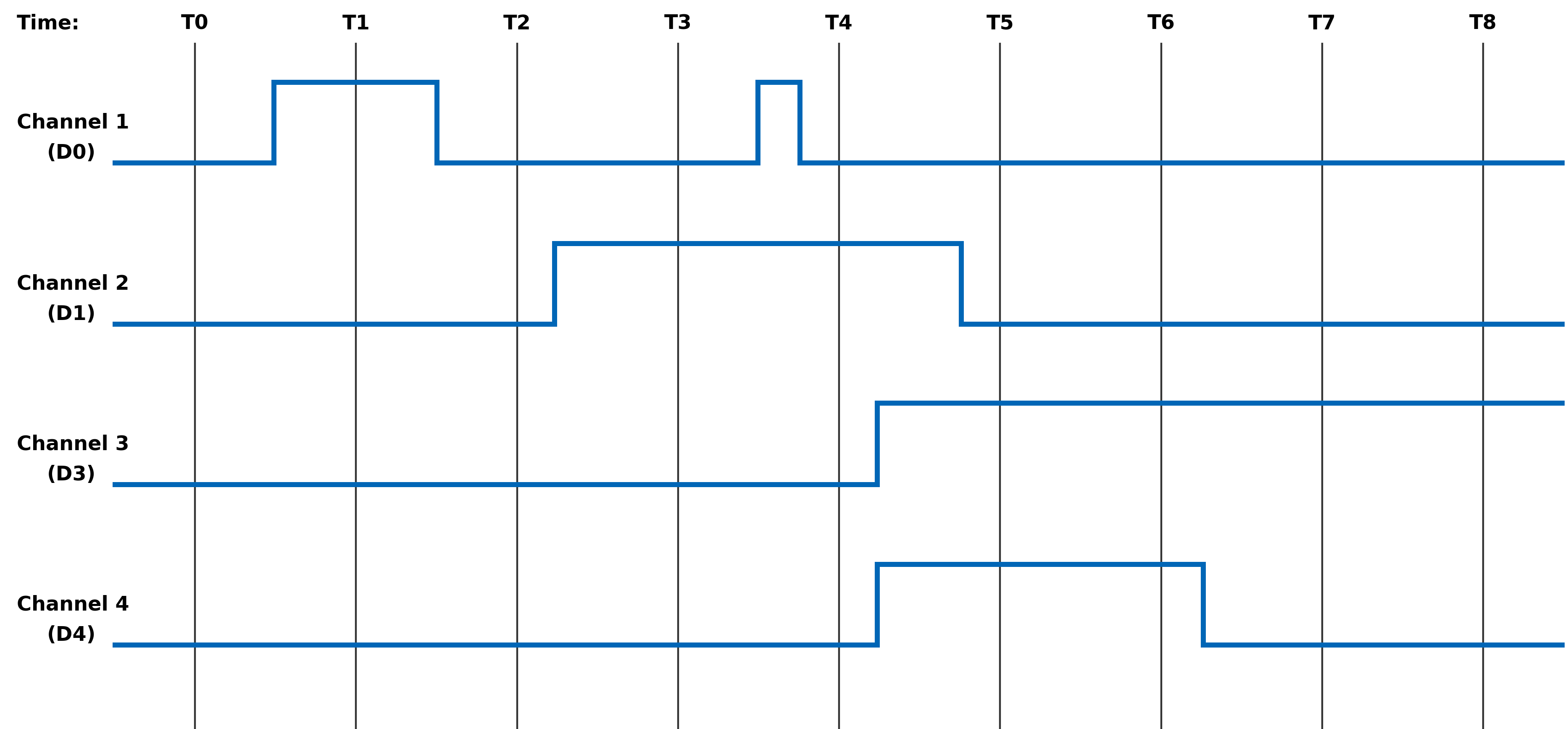
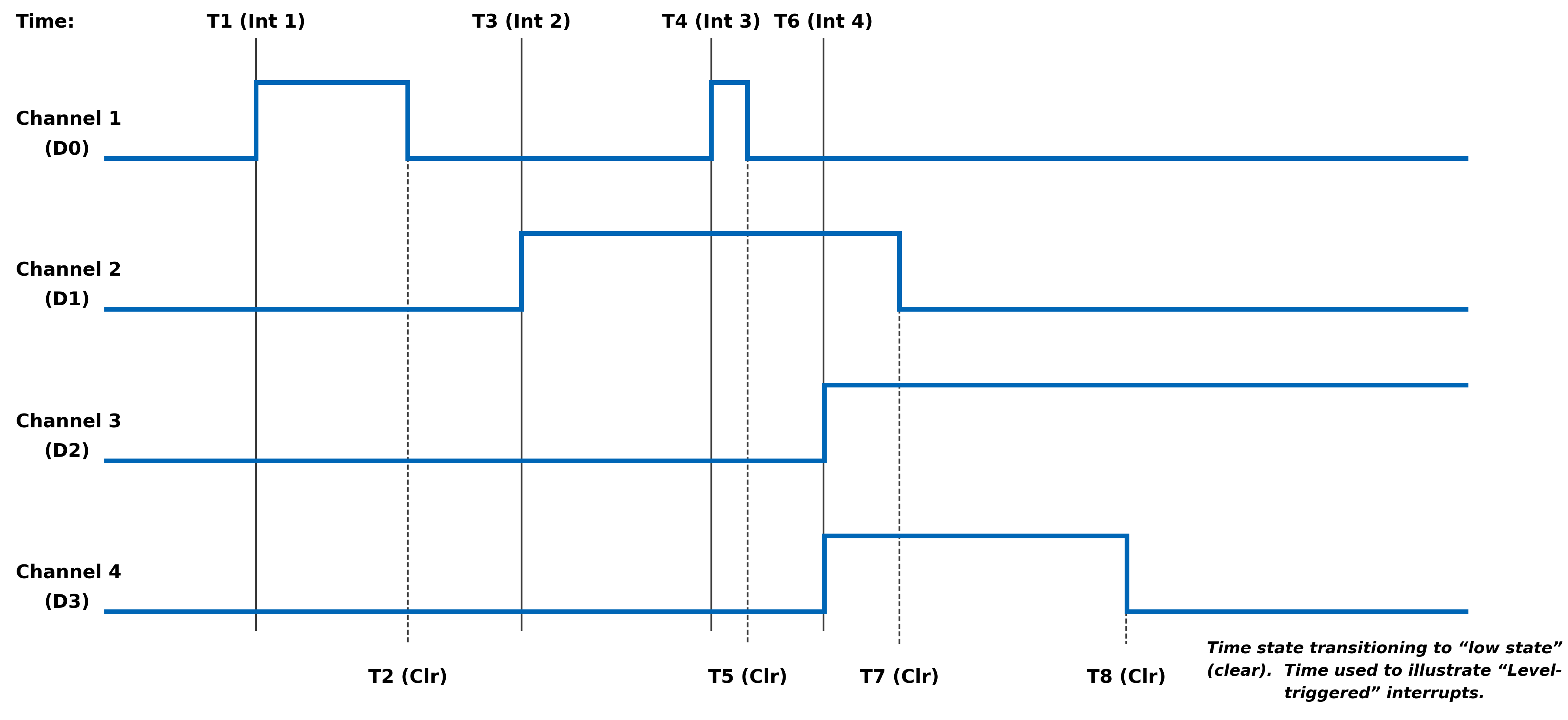
THRESHOLD AND SATURATION CAPABILITY
The Threshold and Saturation Capability is available on the following modules:
Analog-to-Digital (A/D) Modules
AD1 - 12 Channels Analog-to-Digital (Voltage Input Only) (±10 to ±1.25 VDC FSR)
AD2 - 12 Channels Analog-to-Digital (Voltage Input Only) (±100 to ±12.5 VDC FSR)
AD3 - 12 Channels Analog-to-Digital (Current Input Only) (±25 mA FSR)
AD4 - 16 Channels Analog-to-Digital (±10.0 to ±1.25 VDC or ±25 mA FSR)
AD5 - 16 Channels Analog-to-Digital (±50.0 to ±6.25 VDC FSR)
AD6 - 16 Channels Analog-to-Digital (±100 to ±12.5 VDC FSR)
ADE - 16 Channels Analog-to-Digital (Voltage Input Only) (±10 to ±0.625 VDC FSR)
ADF - 16 Channels Analog-to-Digital (Voltage Input Only) (±100 to ±6.25 VDC FSR)
PRINCIPLE OF OPERATION
The AD modules provide the ability to monitor the acquired data and set a status when the specific thresholds are reached.
Threshold Detect
There are two thresholds that can be independently programmed on the A/D modules. These thresholds are used to monitor the acquired data and set a status when the specified thresholds are reached. A configurable hysteresis may also be set to determine when the Threshold Detect registers are cleared. The threshold detection can be configured as a FIFO trigger to capture data based on a specified event. Refer to Figure 1 and Figure 2 for illustrations for Threshold Detect Programming.
Figure 1. Threshold Programming with Hysteresis
Figure 2. Threshold Programming with No Hysteresis
Saturation Programming
A low and high saturation setting that can be independently programmed on the A/D modules. These saturation values are used to monitor the acquired data and set a status when the specified saturation is reached as well as setting the A/D reading to the saturation value. Saturation programming can be used to prevent the A/D reading from exceeding the saturation value. Refer to Figure 3 for illustrations of Saturation Programming
Figure 3. Saturation Programming
REGISTER DESCRIPTIONS
The register descriptions provide the register name, Type, Data Range, Read or Write information, Initialized Value, and a description of the function.
Threshold Detect Programming Registers
There are two threshold and hysteresis registers that can be independently programmed on the A/D modules.
Threshold Detect Level
The Threshold Detect Level registers sets the first and second threshold level values.
Threshold Detect Level 1 Function: Sets the first threshold level value Type: signed binary word (32-bit) (Integer Mode) or Single Precision Floating Point Value (IEEE-754) (Floating Point Mode) Data Range: Voltage Threshold Level values are dependent on Polarity and Range settings for the channel. Enable Floating Point Mode: 0 (Integer Mode) ` Unipolar: (AD4-AD6, ADE-ADF) 0x0000 0000 to 0x0000 FFFF ` (AD1-AD3): 0x0000 0000 to 0x00FF FFFF ` Bipolar (2's complement. 24-bit value sign extended to 32 bits): ` (AD4-AD6, ADE-ADF) 0xFFFF 8000 to 0x0000 7FFF; ` (AD1-AD3): 0xFF80 0000 to 0x007F FFFF Enable Floating Point Mode: 1 (Floating Point Mode) ` Single Precision Floating Point Value (IEEE-754) Read/Write: R/W Initialized Value: 90% of full scale (bipolar)
Threshold Detect Level 2 Function: Sets the second threshold level value. Type: signed binary word (32-bit) (Integer Mode) or Single Precision Floating Point Value (IEEE-754) (Floating Point Mode) Data Range: Voltage Threshold Level values are dependent on Polarity and Range settings for the channel. Enable Floating Point Mode: 0 (Integer Mode) ` Unipolar: (AD4-AD6, ADE-ADF) 0x0000 0000 to 0x0000 FFFF ` (AD1-AD3): 0x0000 0000 to 0x00FF FFFF ` Bipolar (2's complement. 24-bit value sign extended to 32 bits): ` (AD4-AD6, ADE-ADF) 0xFFFF 8000 to 0x0000 7FFF; ` (AD1-AD3): 0xFF80 0000 to 0x007F FFFF Enable Floating Point Mode: 1 (Floating Point Mode) ` Single Precision Floating Point Value (IEEE-754) Read/Write: R/W Initialized Value: -90% of full scale (bipolar) Threshold Detect Hysteresis
The Threshold Detect Hysteresis registers sets the first and second threshold hysteresis values. Note, the hysteresis value must be a positive value.
Threshold Detect Hysteresis 1 Function: Sets the first threshold hysteresis value. This value must be positive. Type: signed binary word (32-bit) or Single Precision Floating Point Value (IEEE-754) (Floating Point Mode) Data Range: Voltage Threshold Hysteresis values are dependent on Polarity and Range settings for the channel. Enable Floating Point Mode: 0 (Integer Mode) ` Unipolar: (AD4-AD6, ADE-ADF) 0x0000 0000 to 0x0000 FFFF ` (AD1-AD3): 0x0000 0000 to 0x00FF FFFF ` Bipolar (2's complement. 24-bit value sign extended to 32 bits): ` (AD4-AD6, ADE-ADF) 0xFFFF 8000 to 0x0000 7FFF; ` (AD1-AD3): 0xFF80 0000 to 0x007F FFFF Enable Floating Point Mode: 1 (Floating Point Mode) ` Single Precision Floating Point Value (IEEE-754) Read/Write: R/W Initialized Value: 0
Threshold Detect Hysteresis 2 Function: Sets the second threshold hysteresis value. This value must be positive. Type: signed binary word (32-bit) or Single Precision Floating Point Value (IEEE-754) (Floating Point Mode) Data Range: Voltage Threshold Hysteresis values are dependent on Polarity and Range settings for the channel. Enable Floating Point Mode: 0 (Integer Mode) ` Unipolar: (AD4-AD6, ADE-ADF) 0x0000 0000 to 0x0000 FFFF ` (AD1-AD3): 0x0000 0000 to 0x00FF FFFF ` Bipolar (2's complement. 24-bit value sign extended to 32 bits): ` (AD4-AD6, ADE-ADF) 0xFFFF 8000 to 0x0000 7FFF; ` (AD1-AD3): 0xFF80 0000 to 0x007F FFFF Enable Floating Point Mode: 1 (Floating Point Mode) ` Single Precision Floating Point Value (IEEE-754) Read/Write: R/W Initialized Value: 0 Threshold Detect Control
Threshold Detect Control Function: Sets up detect control for the two thresholds for each channel. Type: unsigned binary word (32-bit) Data Range: 0x0000 0000 to 0xFFFF FFFF Read/Write: R/W Initialized Value: 0 Operational Settings: Set bit to 0 to detect above the threshold level. Set bit to 1 to detect below the threshold level.
AD1-AD3 D31 D30 D29 D28 D27 D26 D25 D24 D23 D22 D21 D20 D19 D18 D17 D16 0 0 0 0 0 0 0 0 Ch12 Ch11 Ch10 Ch9 T2 T1 T2 T1 T2 T1 T2 T1 D D D D D D D D AD4-AD6 and ADE-ADF D31 D30 D29 D28 D27 D26 D25 D24 D23 D22 D21 D20 D19 D18 D17 D16 Ch16 Ch15 Ch14 Ch13 Ch12 Ch11 Ch10 Ch9 T2 T1 T2 T1 T2 T1 T2 T1 T2 T1 T2 T1 T2 T1 T2 T1 D D D D D D D D D D D D D D D D All A/D Modules D15 D14 D13 D12 D11 D10 D9 D8 D7 D6 D5 D4 D3 D2 D1 D0 Ch8 Ch7 Ch6 Ch5 Ch4 Ch3 Ch2 Ch1 T2 T1 T2 T1 T2 T1 T2 T1 T2 T1 T2 T1 T2 T1 T2 T1 D D D D D D D D D D D D D D D D Saturation Programming Registers
A low and high saturation setting that can be independently programmed on the A/D modules.
Saturation Value
The Low Saturation Value registers sets value to report as A/D reading and sets the Saturation Status bit when the A/D data is below the low saturation value. The High Saturation Value registers sets value to report as A/D reading and sets the Saturation Status bit when the A/D data is above the high saturation value.
Low Saturation Function: Sets the low saturation value. Type: signed binary word (32-bit) or Single Precision Floating Point Value (IEEE-754) (Floating Point Mode) Data Range: Saturation Voltage values are dependent on Polarity and Range settings for the channel. Enable Floating Point Mode: 0 (Integer Mode) ` Unipolar: (AD4-AD6, ADE-ADF) 0x0000 0000 to 0x0000 FFFF ` (AD1-AD3): 0x0000 0000 to 0x00FF FFFF ` Bipolar (2's complement. 24-bit value sign extended to 32 bits): ` (AD4-AD6, ADE-ADF) 0xFFFF 8000 to 0x0000 7FFF; ` (AD1-AD3): 0xFF80 0000 to 0x007F FFFF Enable Floating Point Mode: 1 (Floating Point Mode) ` Single Precision Floating Point Value (IEEE-754) Read/Write: R/W Initialized Value: 0
High Saturation Function: Sets the high saturation value. Type: signed binary word (32-bit) or Single Precision Floating Point Value (IEEE-754) (Floating Point Mode) Data Range: Saturation Voltage values are dependent on Polarity and Range settings for the channel. Enable Floating Point Mode: 0 (Integer Mode) ` Unipolar: (AD4-AD6, ADE-ADF) 0x0000 0000 to 0x0000 FFFF ` (AD1-AD3): 0x0000 0000 to 0x00FF FFFF ` Bipolar (2's complement. 24-bit value sign extended to 32 bits): ` (AD4-AD6, ADE-ADF) 0xFFFF 8000 to 0x0000 7FFF; ` (AD1-AD3): 0xFF80 0000 to 0x007F FFFF Enable Floating Point Mode: 1 (Floating Point Mode) ` Single Precision Floating Point Value (IEEE-754) Read/Write: R/W Initialized Value: 0
Saturation Control Function: Sets up saturation control for the two saturation levels for each channel. Type: unsigned binary word (32-bit) Data Range: 0x0000 0000 to 0xFFFF FFFF Read/Write: R/W Initialized Value: 0 Operational Settings: Set bits to 1 to enable Saturation Control. Set bits to 0 to disable Saturation Control. Each channel control consists of two bits: Low Saturation Control ("Even' bits (B0, B2, B4,...)) and High Saturation Control ("Odd' bits (B1, B3, B5,...)).
AD1-AD3 D31 D30 D29 D28 D27 D26 D25 D24 D23 D22 D21 D20 D19 D18 D17 D16 0 0 0 0 0 0 0 0 Ch12 Ch11 Ch10 Ch9 High Low High Low High Low High Low D D D D D D D D AD4-AD6 and ADE-ADF D31 D30 D29 D28 D27 D26 D25 D24 D23 D22 D21 D20 D19 D18 D17 D16 Ch16 Ch15 Ch14 Ch13 Ch12 Ch11 Ch10 Ch9 High Low High Low High Low High Low High Low High Low High Low High Low D D D D D D D D D D D D D D D D All A/D Modules D15 D14 D13 D12 D11 D10 D9 D8 D7 D6 D5 D4 D3 D2 D1 D0 Ch8 Ch7 Ch6 Ch5 Ch4 Ch3 Ch2 Ch1 High Low High Low High Low High Low High Low High Low High Low High Low D D D D D D D D D D D D D D D D Status and Interrupt
The A/D Module provides status registers for Threshold Detect and Saturation.
Threshold Detect Status
There are four registers associated with the Threshold Detect Status: Dynamic, Latched, Interrupt Enable, and Set Edge/Level Interrupt.
0 = Normal; 1 = Outside of threshold range. The status is created based on the values set in the Threshold Detect 1 and Threshold Detect 2 registers. Bits D0 and D1 represent if channel 1 is outside the threshold for Threshold Detect 1 and Threshold Detect 2 respectively, Bits D2 and D3 represent if channel 2 is outside the threshold for Threshold Detect 1 and Threshold Detect 2 respectively, etc. This pattern continues for all channels.
Threshold Detect Status Function: Sets the corresponding bit associated with the channel's Threshold Detect error. Type: unsigned binary word (32-bit) Data Range: 0x0000 0000 to 0x00FF FFFF Read/Write: R (Dynamic), R/W (Latched, Interrupt Enable, Edge/Level Interrupt) Initialized Value: 0
Threshold Detect Dynamic Status Threshold Detect Latched Status Threshold Detect Interrupt Enable Threshold Detect Set Edge/Level Interrupt AD1-AD3 D31 D30 D29 D28 D27 D26 D25 D24 D23 D22 D21 D20 D19 D18 D17 D16 0 0 0 0 0 0 0 0 Ch12 Ch11 Ch10 Ch9 T2 T1 T2 T1 T2 T1 T2 T1 D D D D D D D D AD4-AD6 and ADE-ADF D31 D30 D29 D28 D27 D26 D25 D24 D23 D22 D21 D20 D19 D18 D17 D16 Ch16 Ch15 Ch14 Ch13 Ch12 Ch11 Ch10 Ch9 T2 T1 T2 T1 T2 T1 T2 T1 T2 T1 T2 T1 T2 T1 T2 T1 D D D D D D D D D D D D D D D D All A/D Modules D15 D14 D13 D12 D11 D10 D9 D8 D7 D6 D5 D4 D3 D2 D1 D0 Ch8 Ch7 Ch6 Ch5 Ch4 Ch3 Ch2 Ch1 T2 T1 T2 T1 T2 T1 T2 T1 T2 T1 T2 T1 T2 T1 T2 T1 D D D D D D D D D D D D D D D D Saturation Status
There are four registers associated with the Saturation Status: Dynamic, Latched, Interrupt Enable, and Set Edge/Level Interrupt.
0 = Normal; 1 = Outside of saturation range. The status is created based on the values set in the Low Saturation and High Saturation registers. Bits D0 and D1 represent if channel 1 is outside the voltage for Low Saturation and High Saturation respectively, Bits D2 and D3 represent if channel 2 is outside the voltage for Low Saturation and High Saturation respectively, etc. This pattern continues for all channels.
Saturation Status Function: Sets the corresponding bit associated with the channel's Saturation error. Type: unsigned binary word (32-bit) Data Range: 0x0000 0000 to 0x00FF FFFF Read/Write: R (Dynamic), R/W (Latched, Interrupt Enable, Edge/Level Interrupt) Initialized Value: 0
Saturation Dynamic Status Saturation Latched Status Saturation Interrupt Enable Saturation Set Edge/Level Interrupt AD1-AD3 D31 D30 D29 D28 D27 D26 D25 D24 D23 D22 D21 D20 D19 D18 D17 D16 0 0 0 0 0 0 0 0 Ch12 Ch11 Ch10 Ch9 High Low High Low High Low High Low D D D D D D D D AD4-AD6 and ADE-ADF D31 D30 D29 D28 D27 D26 D25 D24 D23 D22 D21 D20 D19 D18 D17 D16 Ch16 Ch15 Ch14 Ch13 Ch12 Ch11 Ch10 Ch9 High Low High Low High Low High Low High Low High Low High Low High Low D D D D D D D D D D D D D D D D All A/D Modules D15 D14 D13 D12 D11 D10 D9 D8 D7 D6 D5 D4 D3 D2 D1 D0 Ch8 Ch7 Ch6 Ch5 Ch4 Ch3 Ch2 Ch1 High Low High Low High Low High Low High Low High Low High Low High Low D D D D D D D D D D D D D D D D
FUNCTION REGISTER MAP
KEY
Configuration/Control State/Measurement/Status
THRESHOLD DETECT PROGRAMMING REGISTERS **Data is represented in Floating Point if Enable Floating Point Mode register is set to Floating Point Mode (1). NOTE: Base Address - 0x4000 0000 OFFSET REGISTER NAME ACCESS OFFSET REGISTER NAME ACCESS All A/D Modules 0x1980 Threshold Detect Level 1 Ch 1** R/W 0x1A00 Threshold Detect Level 1 Hysteresis Ch 1** R/W 0x1984 Threshold Detect Level 1 Ch 2** R/W 0x1A04 Threshold Detect Level 1 Hysteresis Ch 2** R/W 0x1988 Threshold Detect Level 1 Ch 3** R/W 0x1A08 Threshold Detect Level 1 Hysteresis Ch 3** R/W 0x198C Threshold Detect Level 1 Ch 4** R/W 0x1A0C Threshold Detect Level 1 Hysteresis Ch 4** R/W 0x1990 Threshold Detect Level 1 Ch 5** R/W 0x1A10 Threshold Detect Level 1 Hysteresis Ch 5** R/W 0x1994 Threshold Detect Level 1 Ch 6** R/W 0x1A14 Threshold Detect Level 1 Hysteresis Ch 6** R/W 0x1998 Threshold Detect Level 1 Ch 7** R/W 0x1A18 Threshold Detect Level 1 Hysteresis Ch 7** R/W 0x199C Threshold Detect Level 1 Ch 8** R/W 0x1A1C Threshold Detect Level 1 Hysteresis Ch 8** R/W 0x19A0 Threshold Detect Level 1 Ch 9** R/W 0x1A20 Threshold Detect Level 1 Hysteresis Ch 9** R/W 0x19A4 Threshold Detect Level 1 Ch 10** R/W 0x1A24 Threshold Detect Level 1 Hysteresis Ch 10** R/W 0x19A8 Threshold Detect Level 1 Ch 11** R/W 0x1A28 Threshold Detect Level 1 Hysteresis Ch 11** R/W 0x19AC Threshold Detect Level 1 Ch 12** R/W 0x1A2C Threshold Detect Level 1 Hysteresis Ch 12** R/W AD4-AD6, ADE-ADF 0x19B0 Threshold Detect Level 1 Ch 13** R/W 0x1A30 Threshold Detect Level 1 Hysteresis Ch 13** R/W 0x19B4 Threshold Detect Level 1 Ch 14** R/W 0x1A34 Threshold Detect Level 1 Hysteresis Ch 14** R/W 0x19B8 Threshold Detect Level 1 Ch 15** R/W 0x1A38 Threshold Detect Level 1 Hysteresis Ch 15** R/W 0x19BC Threshold Detect Level 1 Ch 16** R/W 0x1A3C Threshold Detect Level 1 Hysteresis Ch 16** R/W All A/D Modules 0x1A80 Threshold Detect Level 2 Ch 1** R/W 0x1B00 Threshold Detect Level 2 Hysteresis Ch 1** R/W 0x1A84 Threshold Detect Level 2 Ch 2** R/W 0x1B04 Threshold Detect Level 2 Hysteresis Ch 2** R/W 0x1A88 Threshold Detect Level 2 Ch 3** R/W 0x1B08 Threshold Detect Level 2 Hysteresis Ch 3** R/W 0x1A8C Threshold Detect Level 2 Ch 4** R/W 0x1B0C Threshold Detect Level 2 Hysteresis Ch 4** R/W 0x1A90 Threshold Detect Level 2 Ch 5** R/W 0x1B10 Threshold Detect Level 2 Hysteresis Ch 5** R/W 0x1A94 Threshold Detect Level 2 Ch 6** R/W 0x1B14 Threshold Detect Level 2 Hysteresis Ch 6** R/W 0x1A98 Threshold Detect Level 2 Ch 7** R/W 0x1B18 Threshold Detect Level 2 Hysteresis Ch 7** R/W 0x1A9C Threshold Detect Level 2 Ch 8** R/W 0x1B1C Threshold Detect Level 2 Hysteresis Ch 8** R/W 0x1AA0 Threshold Detect Level 2 Ch 9** R/W 0x1B20 Threshold Detect Level 2 Hysteresis Ch 9** R/W 0x1AA4 Threshold Detect Level 2 Ch 10** R/W 0x1B24 Threshold Detect Level 2 Hysteresis Ch 10** R/W 0x1AA8 Threshold Detect Level 2 Ch 11** R/W 0x1B28 Threshold Detect Level 2 Hysteresis Ch 11** R/W 0x1AAC Threshold Detect Level 2 Ch 12** R/W 0x1B2C Threshold Detect Level 2 Hysteresis Ch 12** R/W AD4-AD6, ADE-ADF 0x1AB0 Threshold Detect Level 2 Ch 13** R/W 0x1B30 Threshold Detect Level 2 Hysteresis Ch 13** R/W 0x1AB4 Threshold Detect Level 2 Ch 14** R/W 0x1B34 Threshold Detect Level 2 Hysteresis Ch 14** R/W 0x1AB8 Threshold Detect Level 2 Ch 15** R/W 0x1B38 Threshold Detect Level 2 Hysteresis Ch 15** R/W 0x1ABC Threshold Detect Level 2 Ch 16** R/W 0x1B3C Threshold Detect Level 2 Hysteresis Ch 16** R/W 0x1C80 Threshold Detect Control R/W
SATURATION PROGRAMMING REGISTERS **Data is represented in Floating Point if Enable Floating Point Mode register is set to Floating Point Mode (1). NOTE: Base Address - 0x4000 0000 OFFSET REGISTER NAME ACCESS OFFSET REGISTER NAME ACCESS All A/D Modules 0x1B80 Low Saturation Value Ch 1** R/W 0x1C00 High Saturation Value Ch 1** R/W 0x1B84 Low Saturation Value Ch 2** R/W 0x1C04 High Saturation Value Ch 2** R/W 0x1B88 Low Saturation Value Ch 3** R/W 0x1C08 High Saturation Value Ch 3** R/W 0x1B8C Low Saturation Value Ch 4** R/W 0x1C0C High Saturation Value Ch 4** R/W 0x1B90 Low Saturation Value Ch 5** R/W 0x1C10 High Saturation Value Ch 5** R/W 0x1B94 Low Saturation Value Ch 6** R/W 0x1C14 High Saturation Value Ch 6** R/W 0x1B98 Low Saturation Value Ch 7** R/W 0x1C18 High Saturation Value Ch 7** R/W 0x1B9C Low Saturation Value Ch 8** R/W 0x1C1C High Saturation Value Ch 8** R/W 0x1BA0 Low Saturation Value Ch 9** R/W 0x1C20 High Saturation Value Ch 9** R/W 0x1BA4 Low Saturation Value Ch 10** R/W 0x1C24 High Saturation Value Ch 10** R/W 0x1BA8 Low Saturation Value Ch 11** R/W 0x1C28 High Saturation Value Ch 11** R/W 0x1BAC Low Saturation Value Ch 12** R/W 0x1C2C High Saturation Value Ch 12** R/W AD4-AD6, ADE-ADF 0x1BB0 Low Saturation Value Ch 13** R/W 0x1C30 High Saturation Value Ch 13** R/W 0x1BB4 Low Saturation Value Ch 14** R/W 0x1C34 High Saturation Value Ch 14** R/W 0x1BB8 Low Saturation Value Ch 15** R/W 0x1C38 High Saturation Value Ch 15** R/W 0x1BBC Low Saturation Value Ch 16** R/W 0x1C3C High Saturation Value Ch 16** R/W 0x1C90 Saturation Control R/W
STATUS REGISTERS *When an event is detected, the bit associated with the event is set in this register and will remain set until the user clears the event bit. Clearing the bit requires writing a 1 back to the specific bit that was set when read (i.e., write-1-to-clear, writing a “1” to a bit set to “1” will set the bit to “0). NOTE: Base Address - 0x4000 0000 OFFSET REGISTER NAME ACCESS OFFSET REGISTER NAME ACCESS Threshold Saturation 0x0940 Dynamic Status R 0x0960 Dynamic Status R 0x0944 Latched Status* R/W 0x0964 Latched Status* R/W 0x0948 Interrupt Enable R/W 0x0968 Interrupt Enable R/W 0x094C Set Edge/Level Interrupt R/W 0x096C Set Edge/Level Interrupt R/W
INTERRUPT REGISTERS The Interrupt Vector and Interrupt Steering registers are located on the Motherboard Memory Space and do not require any Module Address Offsets. These registers are accessed using the absolute addresses listed in the table below. OFFSET REGISTER NAME ACCESS OFFSET REGISTER NAME ACCESS 0x0550 Module 1 Interrupt Vector 21 - Threshold Status R/W 0x0650 Module 1 Interrupt Steering 21 - Threshold Status R/W 0x0558 Module 1 Interrupt Vector 23 - Saturation Status R/W 0x0658 Module 1 Interrupt Steering 23 - Saturation Status R/W 0x0750 Module 2 Interrupt Vector 21 - Threshold Status R/W 0x0850 Module 2 Interrupt Steering 21 - Threshold Status R/W 0x0758 Module 2 Interrupt Vector 23 - Saturation Status R/W 0x0858 Module 2 Interrupt Steering 23 - Saturation Status R/W 0x0950 Module 3 Interrupt Vector 21 - Threshold Status R/W 0x0A50 Module 3 Interrupt Steering 21 - Threshold Status R/W 0x0958 Module 3 Interrupt Vector 23 - Saturation Status R/W 0x0A58 Module 3 Interrupt Steering 23 - Saturation Status R/W 0x0B50 Module 4 Interrupt Vector 21 - Threshold Status R/W 0x0C50 Module 4 Interrupt Steering 21 - Threshold Status R/W 0x0B58 Module 4 Interrupt Vector 23 - Saturation Status R/W 0x0C58 Module 4 Interrupt Steering 23 - Saturation Status R/W 0x0D50 Module 5 Interrupt Vector 21 - Threshold Status R/W 0x0E50 Module 5 Interrupt Steering 21 - Threshold Status R/W 0x0D58 Module 5 Interrupt Vector 23 - Saturation Status R/W 0x0E58 Module 5 Interrupt Steering 23 - Saturation Status R/W 0x0F50 Module 6 Interrupt Vector 21 - Threshold Status R/W 0x1050 Module 6 Interrupt Steering 21 - Threshold Status R/W 0x0F58 Module 6 Interrupt Vector 23 - Saturation Status R/W 0x1058 Module 6 Interrupt Steering 23 - Saturation Status R/W REVISION HISTORY
Module Manual - AD Threshold and Saturation Programming Revision History Revision Revision Date Description C 2021-11-30 C08896; Transition manual to docbuilder format - no technical information change. C1 2022-03-16 C09163, pg.15-17, changed "AD4-AD4" to "AD4-AD6". C2 2023-01-24 ECO C010010, pg.8-9/11, added 24-bit integer mode data ranges. C3 2023-06-20 ECO C10476, removed all ADG module references from manual. C4 2024-04-18 ECO C11441, spelling correction ('2's compliment' to '2's complement); no technical info change. DOCS.NAII REVISIONS
Link to original
Revision Date Description 2026-05-18 Formatting updates throughout manual (non-technical changes).
MODULE COMMON REGISTERS
The registers described in this document are common to all NAI Generation 5 modules.
Module Information Registers
The registers in this section provide module information such as firmware revisions, capabilities and unique serial number information.
FPGA Version Registers
The FPGA firmware version registers include registers that contain the Revision, Compile Timestamp, SerDes Revision, Template Revision and Zynq Block Revision information.
FPGA Revision Function: FPGA firmware revision Type: unsigned binary word (32-bit) Data Range: 0x0000 0000 to 0xFFFF FFFF Read/Write: R Initialized Value: Value corresponding to the revision of the board's FPGA Operational Settings: The upper 16-bits are the major revision and the lower 16-bits are the minor revision.
D31 D30 D29 D28 D27 D26 D25 D24 D23 D22 D21 D20 D19 D18 D17 D16 Major Revision Number D15 D14 D13 D12 D11 D10 D9 D8 D7 D6 D5 D4 D3 D2 D1 D0 Minor Revision Number
FPGA Compile Timestamp Function: Compile Timestamp for the FPGA firmware. Type: unsigned binary word (32-bit) Data Range: N/A Read/Write: R Initialized Value: Value corresponding to the compile timestamp of the board's FPGA Operational Settings: The 32-bit value represents the Day, Month, Year, Hour, Minutes and Seconds as formatted in the table:
D31 D30 D29 D28 D27 D26 D25 D24 D23 D22 D21 D20 D19 D18 D17 D16 day (5-bits) month (4-bits) year (6-bits) hr D15 D14 D13 D12 D11 D10 D9 D8 D7 D6 D5 D4 D3 D2 D1 D0 hour (5-bits) minutes (6-bits) seconds (6-bits)
FPGA SerDes Revision Function: FPGA SerDes revision Type: unsigned binary word (32-bit) Data Range: 0x0000 0000 to 0xFFFF FFFF Read/Write: R Initialized Value: Value corresponding to the SerDes revision of the board's FPGA Operational Settings: The upper 16-bits are the major revision, and the lower 16-bits are the minor revision.
D31 D30 D29 D28 D27 D26 D25 D24 D23 D22 D21 D20 D19 D18 D17 D16 Major Revision Number D15 D14 D13 D12 D11 D10 D9 D8 D7 D6 D5 D4 D3 D2 D1 D0 Minor Revision Number
FPGA Template Revision Function: FPGA Template revision Type: unsigned binary word (32-bit) Data Range: 0x0000 0000 to 0xFFFF FFFF Read/Write: R Initialized Value: Value corresponding to the template revision of the board's FPGA Operational Settings: The upper 16-bits are the major revision, and the lower 16-bits are the minor revision.
D31 D30 D29 D28 D27 D26 D25 D24 D23 D22 D21 D20 D19 D18 D17 D16 Major Revision Number D15 D14 D13 D12 D11 D10 D9 D8 D7 D6 D5 D4 D3 D2 D1 D0 Minor Revision Number
FPGA Zynq Block Revision Function: FPGA Zynq Block revision Type: unsigned binary word (32-bit) Data Range: 0x0000 0000 to 0xFFFF FFFF Read/Write: R Initialized Value: Value corresponding to the Zynq block revision of the board's FPGA Operational Settings: The upper 16-bits are the major revision, and the lower 16-bits are the minor revision.
D31 D30 D29 D28 D27 D26 D25 D24 D23 D22 D21 D20 D19 D18 D17 D16 Major Revision Number D15 D14 D13 D12 D11 D10 D9 D8 D7 D6 D5 D4 D3 D2 D1 D0 Minor Revision Number Bare Metal Version Registers
The Bare Metal firmware version registers include registers that contain the Revision and Compile Time information.
Bare Metal Revision Function: Bare Metal firmware revision Type: unsigned binary word (32-bit) Data Range: 0x0000 0000 to 0xFFFF FFFF Read/Write: R Initialized Value: Value corresponding to the revision of the board's Bare Metal Operational Settings: The upper 16-bits are the major revision and the lower 16-bits are the minor revision.
D31 D30 D29 D28 D27 D26 D25 D24 D23 D22 D21 D20 D19 D18 D17 D16 Major Revision Number D15 D14 D13 D12 D11 D10 D9 D8 D7 D6 D5 D4 D3 D2 D1 D0 Minor Revision Number
Bare Metal Compile Time Function: Provides an ASCII representation of the Date/Time for the Bare Metal compile time. Type: 24-character ASCII string - Six (6) unsigned binary word (32-bit) Data Range: N/A Read/Write: R Initialized Value: Value corresponding to the ASCII representation of the compile time of the board's Bare Metal Operational Settings: The six 32-bit words provide an ASCII representation of the Date/Time. The hexadecimal values in the field below represent: May 17 2019 at 15:38:32 Note
little-endian order of ASCII values
Word 1 (Ex. 0x2079614D) D31 D30 D29 D28 D27 D26 D25 D24 D23 D22 D21 D20 D19 D18 D17 D16 Space (0x20) Month ('y' - 0x79) D15 D14 D13 D12 D11 D10 D9 D8 D7 D6 D5 D4 D3 D2 D1 D0 Month ('a' - 0x61) Month ('M' - 0x4D) Word 2 (Ex. 0x32203731) D31 D30 D29 D28 D27 D26 D25 D24 D23 D22 D21 D20 D19 D18 D17 D16 Year ('2' - 0x32) Space (0x20) D15 D14 D13 D12 D11 D10 D9 D8 D7 D6 D5 D4 D3 D2 D1 D0 Day ('7' - 0x37) Day ('1' - 0x31) Word 3 (Ex. 0x20393130) D31 D30 D29 D28 D27 D26 D25 D24 D23 D22 D21 D20 D19 D18 D17 D16 Space (0x20) Year ('9' - 0x39) D15 D14 D13 D12 D11 D10 D9 D8 D7 D6 D5 D4 D3 D2 D1 D0 Year ('1' - 0x31) Year ('0' - 0x30) Word 4 (Ex. 0x31207461) D31 D30 D29 D28 D27 D26 D25 D24 D23 D22 D21 D20 D19 D18 D17 D16 Hour ('1' - 0x31) Space (0x20) D15 D14 D13 D12 D11 D10 D9 D8 D7 D6 D5 D4 D3 D2 D1 D0 'a' (0x74) 't' (0x61) Word 5 (Ex. 0x38333A35) D31 D30 D29 D28 D27 D26 D25 D24 D23 D22 D21 D20 D19 D18 D17 D16 Minute ('8' - 0x38) Minute ('3' - 0x33) D15 D14 D13 D12 D11 D10 D9 D8 D7 D6 D5 D4 D3 D2 D1 D0 ':' (0x3A) Hour ('5' - 0x35) Word 6 (Ex. 0x0032333A) D31 D30 D29 D28 D27 D26 D25 D24 D23 D22 D21 D20 D19 D18 D17 D16 NULL (0x00) Seconds ('2' - 0x32) D15 D14 D13 D12 D11 D10 D9 D8 D7 D6 D5 D4 D3 D2 D1 D0 Seconds ('3' - 0x33) ':' (0x3A) FSBL Version Registers
The FSBL version registers include registers that contain the Revision and Compile Time information for the First Stage Boot Loader (FSBL).
FSBL Revision Function: FSBL firmware revision Type: unsigned binary word (32-bit) Data Range: 0x0000 0000 to 0xFFFF FFFF Read/Write: R Initialized Value: Value corresponding to the revision of the board's FSBL Operational Settings: The upper 16-bits are the major revision, and the lower 16-bits are the minor revision.
D31 D30 D29 D28 D27 D26 D25 D24 D23 D22 D21 D20 D19 D18 D17 D16 Major Revision Number D15 D14 D13 D12 D11 D10 D9 D8 D7 D6 D5 D4 D3 D2 D1 D0 Minor Revision Number
FSBL Compile Time Function: Provides an ASCII representation of the Date/Time for the FSBL compile time. Type: 24-character ASCII string - Six (6) unsigned binary word (32-bit) Data Range: N/A Read/Write: R Initialized Value: Value corresponding to the ASCII representation of the Compile Time of the board's FSBL Operational Settings: The six 32-bit words provide an ASCII representation of the Date/Time. The hexadecimal values in the field below represent: May 17 2019 at 15:38:32
Note
little-endian order of ASCII values
Word 1 (Ex. 0x2079614D) D31 D30 D29 D28 D27 D26 D25 D24 D23 D22 D21 D20 D19 D18 D17 D16 Space (0x20) Month ('y' - 0x79) D15 D14 D13 D12 D11 D10 D9 D8 D7 D6 D5 D4 D3 D2 D1 D0 Month ('a' - 0x61) Month ('M' - 0x4D) Word 2 (Ex. 0x32203731) D31 D30 D29 D28 D27 D26 D25 D24 D23 D22 D21 D20 D19 D18 D17 D16 Year ('2' - 0x32) Space (0x20) D15 D14 D13 D12 D11 D10 D9 D8 D7 D6 D5 D4 D3 D2 D1 D0 Day ('7' - 0x37) Day ('1' - 0x31) Word 3 (Ex. 0x20393130) D31 D30 D29 D28 D27 D26 D25 D24 D23 D22 D21 D20 D19 D18 D17 D16 Space (0x20) Year ('9' - 0x39) D15 D14 D13 D12 D11 D10 D9 D8 D7 D6 D5 D4 D3 D2 D1 D0 Year ('1' - 0x31) Year ('0' - 0x30) Word 4 (Ex. 0x31207461) D31 D30 D29 D28 D27 D26 D25 D24 D23 D22 D21 D20 D19 D18 D17 D16 Hour ('1' - 0x31) Space (0x20) D15 D14 D13 D12 D11 D10 D9 D8 D7 D6 D5 D4 D3 D2 D1 D0 'a' (0x74) 't' (0x61) Word 5 (Ex. 0x38333A35) D31 D30 D29 D28 D27 D26 D25 D24 D23 D22 D21 D20 D19 D18 D17 D16 Minute ('8' - 0x38) Minute ('3' - 0x33) D15 D14 D13 D12 D11 D10 D9 D8 D7 D6 D5 D4 D3 D2 D1 D0 ':' (0x3A) Hour ('5' - 0x35) Word 6 (Ex. 0x0032333A) D31 D30 D29 D28 D27 D26 D25 D24 D23 D22 D21 D20 D19 D18 D17 D16 NULL (0x00) Seconds ('2' - 0x32) D15 D14 D13 D12 D11 D10 D9 D8 D7 D6 D5 D4 D3 D2 D1 D0 Seconds ('3' - 0x33) ':' (0x3A) Module Serial Number Registers
The Module Serial Number registers include registers that contain the Serial Numbers for the Interface Board and the Functional Board of the module.
Interface Board Serial Number Function: Unique 128-bit identifier used to identify the interface board. Type: 16-character ASCII string - Four (4) unsigned binary words (32-bit) Data Range: N/A Read/Write: R Initialized Value: Serial number of the interface board Operational Settings: This register is for information purposes only.
Functional Board Serial Number Function: Unique 128-bit identifier used to identify the functional board. Type: 16-character ASCII string - Four (4) unsigned binary words (32-bit) Data Range: N/A Read/Write: R Initialized Value: Serial number of the functional board Operational Settings: This register is for information purposes only.
Module Capability Function: Provides indication for whether or not the module can support the following: SerDes block reads, SerDes FIFO block reads, SerDes packing (combining two 16-bit values into one 32-bit value) and floating point representation. The purpose for block access and packing is to improve the performance of accessing larger amounts of data over the SerDes interface. Type: unsigned binary word (32-bit) Data Range: 0x0000 0000 to 0x0000 0107 Read/Write: R Initialized Value: 0x0000 0107 Operational Settings: A “1” in the bit associated with the capability indicates that it is supported.
D31 D30 D29 D28 D27 D26 D25 D24 D23 D22 D21 D20 D19 D18 D17 D16 0 0 0 0 0 0 0 0 0 0 0 0 0 0 0 0 D15 D14 D13 D12 D11 D10 D9 D8 D7 D6 D5 D4 D3 D2 D1 D0 0 0 0 0 0 0 0 Flt-Pt 0 0 0 0 0 Pack FIFO Blk Blk
Module Memory Map Revision Function: Module Memory Map revision Type: unsigned binary word (32-bit) Data Range: 0x0000 0000 to 0xFFFF FFFF Read/Write: R Initialized Value: Value corresponding to the Module Memory Map Revision Operational Settings: The upper 16-bits are the major revision and the lower 16-bits are the minor revision.
D31 D30 D29 D28 D27 D26 D25 D24 D23 D22 D21 D20 D19 D18 D17 D16 Major Revision Number D15 D14 D13 D12 D11 D10 D9 D8 D7 D6 D5 D4 D3 D2 D1 D0 Minor Revision Number Module Measurement Registers
The registers in this section provide module temperature measurement information.
Temperature Readings Registers
The temperature registers provide the current, maximum (from power-up) and minimum (from power-up) Zynq and PCB temperatures.
Interface Board Current Temperature Function: Measured PCB and Zynq Core temperatures on Interface Board. Type: signed byte (8-bits) for PCB and signed byte (8-bits) for Zynq core temperatures Data Range: 0x0000 0000 to 0x0000 FFFF Read/Write: R Initialized Value: Value corresponding to the measured PCB and Zynq core temperatures based on the table below Operational Settings: The upper 16-bits are not used, and the lower 16-bits are the PCB and Zynq Core Temperatures. For example, if the register contains the value 0x0000 202C, this represents PCB Temperature = 32° Celsius and Zynq Temperature = 44° Celsius.
D31 D30 D29 D28 D27 D26 D25 D24 D23 D22 D21 D20 D19 D18 D17 D16 0 0 0 0 0 0 0 0 0 0 0 0 0 0 0 0 D15 D14 D13 D12 D11 D10 D9 D8 D7 D6 D5 D4 D3 D2 D1 D0 PCB Temperature Zynq Core Temperature
Functional Board Current Temperature Function: Measured PCB temperature on Functional Board. Type: signed byte (8-bits) for PCB Data Range: 0x0000 0000 to 0x0000 00FF Read/Write: R Initialized Value: Value corresponding to the measured PCB on the table below Operational Settings: The upper 24-bits are not used, and the lower 8-bits are the PCB Temperature. For example, if the register contains the value 0x0000 0019, this represents PCB Temperature = 25° Celsius.
D31 D30 D29 D28 D27 D26 D25 D24 D23 D22 D21 D20 D19 D18 D17 D16 0 0 0 0 0 0 0 0 0 0 0 0 0 0 0 0 D15 D14 D13 D12 D11 D10 D9 D8 D7 D6 D5 D4 D3 D2 D1 D0 0 0 0 0 0 0 0 0 PCB Temperature
Interface Board Maximum Temperature Function: Maximum PCB and Zynq Core temperatures on Interface Board since power-on. Type: signed byte (8-bits) for PCB and signed byte (8-bits) for Zynq core temperatures Data Range: 0x0000 0000 to 0x0000 FFFF Read/Write: R Initialized Value: Value corresponding to the maximum measured PCB and Zynq core temperatures since power-on based on the table below Operational Settings: The upper 16-bits are not used, and the lower 16-bits are the maximum PCB and Zynq Core Temperatures. For example, if the register contains the value 0x0000 5569, this represents maximum PCB Temperature = 85° Celsius and maximum Zynq Temperature = 105° Celsius.
D31 D30 D29 D28 D27 D26 D25 D24 D23 D22 D21 D20 D19 D18 D17 D16 0 0 0 0 0 0 0 0 0 0 0 0 0 0 0 0 D15 D14 D13 D12 D11 D10 D9 D8 D7 D6 D5 D4 D3 D2 D1 D0 PCB Temperature Zynq Core Temperature
Interface Board Minimum Temperature Function: Minimum PCB and Zynq Core temperatures on Interface Board since power-on. Type: signed byte (8-bits) for PCB and signed byte (8-bits) for Zynq core temperatures Data Range: 0x0000 0000 to 0x0000 FFFF Read/Write: R Initialized Value: Value corresponding to the minimum measured PCB and Zynq core temperatures since power-on based on the table below Operational Settings: The upper 16-bits are not used, and the lower 16-bits are the minimum PCB and Zynq Core Temperatures. For example, if the register contains the value 0x0000 D8E7, this represents minimum PCB Temperature = -40° Celsius and minimum Zynq Temperature = -25° Celsius.
D31 D30 D29 D28 D27 D26 D25 D24 D23 D22 D21 D20 D19 D18 D17 D16 0 0 0 0 0 0 0 0 0 0 0 0 0 0 0 0 D15 D14 D13 D12 D11 D10 D9 D8 D7 D6 D5 D4 D3 D2 D1 D0 PCB Temperature Zynq Core Temperature
Functional Board Maximum Temperature Function: Maximum PCB temperature on Functional Board since power-on. Type: signed byte (8-bits) for PCB Data Range: 0x0000 0000 to 0x0000 00FF Read/Write: R Initialized Value: Value corresponding to the measured PCB on the table below Operational Settings: The upper 24-bits are not used, and the lower 8-bits are the PCB Temperature. For example, if the register contains the value 0x0000 0055, this represents PCB Temperature = 85° Celsius.
D31 D30 D29 D28 D27 D26 D25 D24 D23 D22 D21 D20 D19 D18 D17 D16 0 0 0 0 0 0 0 0 0 0 0 0 0 0 0 0 D15 D14 D13 D12 D11 D10 D9 D8 D7 D6 D5 D4 D3 D2 D1 D0 0 0 0 0 0 0 0 0 PCB Temperature
Functional Board Minimum Temperature Function: Minimum PCB temperature on Functional Board since power-on. Type: signed byte (8-bits) for PCB Data Range: 0x0000 0000 to 0x0000 00FF Read/Write: R Initialized Value: Value corresponding to the measured PCB on the table below Operational Settings: The upper 24-bits are not used, and the lower 8-bits are the PCB Temperature. For example, if the register contains the value 0x0000 00D8, this represents PCB Temperature = -40° Celsius.
D31 D30 D29 D28 D27 D26 D25 D24 D23 D22 D21 D20 D19 D18 D17 D16 0 0 0 0 0 0 0 0 0 0 0 0 0 0 0 0 D15 D14 D13 D12 D11 D10 D9 D8 D7 D6 D5 D4 D3 D2 D1 D0 0 0 0 0 0 0 0 0 PCB Temperature Higher Precision Temperature Readings Registers
These registers provide higher precision readings of the current Zynq and PCB temperatures.
Higher Precision Zynq Core Temperature Function: Higher precision measured Zynq Core temperature on Interface Board. Type: signed word (16-bits) for integer part and unsigned word (16-bits) for fractional part Data Range: 0x0000 0000 to 0xFFFF FFFF Read/Write: R Initialized Value: Measured Zynq Core temperature on Interface Board Operational Settings: The upper 16-bits represent the signed integer part of the temperature and the lower 16-bits represent the fractional part of the temperature with the resolution of 1/1000 of degree Celsius. For example, if the register contains the value 0x002B 0271, this represents Zynq Core Temperature = 43.625° Celsius, and value 0xFFF6 0177 represents -10.375° Celsius.
D31 D30 D29 D28 D27 D26 D25 D24 D23 D22 D21 D20 D19 D18 D17 D16 Signed Integer Part of Temperature D15 D14 D13 D12 D11 D10 D9 D8 D7 D6 D5 D4 D3 D2 D1 D0 Fractional Part of Temperature
Higher Precision Interface PCB Temperature Function: Higher precision measured Interface PCB temperature. Type: signed word (16-bits) for integer part and unsigned word (16-bits) for fractional part Data Range: 0x0000 0000 to 0xFFFF FFFF Read/Write: R Initialized Value: Measured Interface PCB temperature Operational Settings: The upper 16-bits represent the signed integer part of the temperature and the lower 16-bits represent the fractional part of the temperature with the resolution of 1/1000 of degree Celsius. For example, if the register contains the value 0x0020 007D, this represents Interface PCB Temperature = 32.125° Celsius, and value 0xFFE8 036B represents -24.875° Celsius.
D31 D30 D29 D28 D27 D26 D25 D24 D23 D22 D21 D20 D19 D18 D17 D16 Signed Integer Part of Temperature D15 D14 D13 D12 D11 D10 D9 D8 D7 D6 D5 D4 D3 D2 D1 D0 Fractional Part of Temperature
Higher Precision Functional PCB Temperature Function: Higher precision measured Functional PCB temperature. Type: signed word (16-bits) for integer part and unsigned word (16-bits) for fractional part Data Range: 0x0000 0000 to 0xFFFF FFFF Read/Write: R Initialized Value: Measured Functional PCB temperature Operational Settings: The upper 16-bits represent the signed integer part of the temperature and the lower 16-bits represent the fractional part of the temperature with the resolution of 1/100 of degree Celsius. For example, if the register contains the value 0x0018 004B, this represents Functional PCB Temperature = 24.75° Celsius, and value 0xFFD9 0019 represents -39.25° Celsius.
D31 D30 D29 D28 D27 D26 D25 D24 D23 D22 D21 D20 D19 D18 D17 D16 Signed Integer Part of Temperature D15 D14 D13 D12 D11 D10 D9 D8 D7 D6 D5 D4 D3 D2 D1 D0 Fractional Part of Temperature Module Health Monitoring Registers
The registers in this section provide module temperature measurement information. If the temperature measurements reaches the Lower Critical or Upper Critical conditions, the module will automatically reset itself to prevent damage to the hardware.
Module Sensor Summary Status Function: The corresponding sensor bit is set if the sensor has crossed any of its thresholds. Type: unsigned binary word (32-bits) Data Range: See table below Read/Write: R Initialized Value: 0 Operational Settings: This register provides a summary for module sensors. When the corresponding sensor bit is set, the Sensor Threshold Status register for that sensor will indicate the threshold condition that triggered the event.
Bit(s) Sensor D31:D6 Reserved D5 Functional Board PCB Temperature D4 Interface Board PCB Temperature D3:D0 Reserved Module Sensor Registers
The registers listed in this section apply to each module sensor listed for the Module Sensor Summary Status register. Each individual sensor register provides a group of registers for monitoring module temperatures readings. From these registers, a user can read the current temperature of the sensor in addition to the minimum and maximum temperature readings since power-up. Upper and lower critical/warning temperature thresholds can be set and monitored from these registers. When a programmed temperature threshold is crossed, the Sensor Threshold Status register will set the corresponding bit for that threshold. The figure below shows the functionality of this group of registers when accessing the Interface Board PCB Temperature sensor as an example.
Sensor Threshold Status Function: Reflects which threshold has been crossed Type: unsigned binary word (32-bits) Data Range: See table below Read/Write: R Initialized Value: 0 Operational Settings: The associated bit is set when the sensor reading exceed the corresponding threshold settings.
Bit(s) Description D31:D4 Reserved D3 Exceeded Upper Critical Threshold D2 Exceeded Upper Warning Threshold D1 Exceeded Lower Critical Threshold D0 Exceeded Lower Warning Threshold
Sensor Current Reading Function: Reflects current reading of temperature sensor Type: Single Precision Floating Point Value (IEEE-754) Data Range: Single Precision Floating Point Value (IEEE-754) Read/Write: R Initialized Value: N/A Operational Settings: The register represents current sensor reading as a single precision floating point value. For example, for a temperature sensor, register value 0x41C6 0000 represents temperature = 24.75° Celsius.
Sensor Minimum Reading Function: Reflects minimum value of temperature sensor since power up Type: Single Precision Floating Point Value (IEEE-754) Data Range: Single Precision Floating Point Value (IEEE-754) Read/Write: R Initialized Value: N/A Operational Settings: The register represents minimum sensor value as a single precision floating point value. For example, for a temperature sensor, register value 0x41C6 0000 represents temperature = 24.75° Celsius.
Sensor Maximum Reading Function: Reflects maximum value of temperature sensor since power up Type: Single Precision Floating Point Value (IEEE-754) Data Range: Single Precision Floating Point Value (IEEE-754) Read/Write: R Initialized Value: N/A Operational Settings: The register represents maximum sensor value as a single precision floating point value. For example, for a temperature sensor, register value 0x41C6 0000 represents temperature = 24.75° Celsius.
Sensor Lower Warning Threshold Function: Reflects lower warning threshold of temperature sensor Type: Single Precision Floating Point Value (IEEE-754) Data Range: Single Precision Floating Point Value (IEEE-754) Read/Write: R/W Initialized Value: Default lower warning threshold (value dependent on specific sensor) Operational Settings: The register represents sensor lower warning threshold as a single precision floating point value. For example, for a temperature sensor, register value 0xC220 0000 represents temperature = -40.0° Celsius.
Sensor Lower Critical Threshold Function: Reflects lower critical threshold of temperature sensor Type: Single Precision Floating Point Value (IEEE-754) Data Range: Single Precision Floating Point Value (IEEE-754) Read/Write: R/W Initialized Value: Default lower critical threshold (value dependent on specific sensor) Operational Settings: The register represents sensor lower critical threshold as a single precision floating point value. For example, for a temperature sensor, register value 0xC25C 0000 represents temperature = -55.0° Celsius.
Sensor Upper Warning Threshold Function: Reflects upper warning threshold of temperature sensor Type: Single Precision Floating Point Value (IEEE-754) Data Range: Single Precision Floating Point Value (IEEE-754) Read/Write: R/W Initialized Value: Default upper warning threshold (value dependent on specific sensor) Operational Settings: The register represents sensor upper warning threshold as a single precision floating point value. For example, for a temperature sensor, register value 0x42AA 0000 represents temperature = 85.0° Celsius.
Sensor Upper Critical Threshold Function: Reflects upper critical threshold of temperature sensor Type: Single Precision Floating Point Value (IEEE-754) Data Range: Single Precision Floating Point Value (IEEE-754) Read/Write: R/W Initialized Value: Default upper critical threshold (value dependent on specific sensor) Operational Settings: The register represents sensor upper critical threshold as a single precision floating point value. For example, for a temperature sensor, register value 0x42FA 0000 represents temperature = 125.0° Celsius. FUNCTION REGISTER MAP
KEY
Configuration/Control Measurement/Status/Board Information
MODULE INFORMATION REGISTERS OFFSET REGISTER NAME ACCESS OFFSET REGISTER NAME ACCESS 0x003C FPGA Revision R 0x0074 Bare Metal Revision R 0x0030 FPGA Compile Timestamp R 0x0080 Bare Metal Compile Time (Bit 0-31) R 0x0034 FPGA SerDes Revision R 0x0084 Bare Metal Compile Time (Bit 32-63) R 0x0038 FPGA Template Revision R 0x0088 Bare Metal Compile Time (Bit 64-95) R 0x0040 FPGA Zynq Block Revision R 0x008C Bare Metal Compile Time (Bit 96-127) R 0x0090 Bare Metal Compile Time (Bit 128-159) R 0x0094 Bare Metal Compile Time (Bit 160-191) R 0x007C FSBL Revision R 0x00B0 FSBL Compile Time (Bit 0-31) R 0x00B4 FSBL Compile Time (Bit 32-63) R 0x00B8 FSBL Compile Time (Bit 64-95) R 0x00BC FSBL Compile Time (Bit 96-127) R 0x00C0 FSBL Compile Time (Bit 128-159) R 0x00C4 FSBL Compile Time (Bit 160-191) R 0x0000 Interface Board Serial Number (Bit 0-31) R 0x0010 Functional Board Serial Number (Bit 0-31) R 0x0034 Interface Board Serial Number (Bit 32-63) R 0x0014 Functional Board Serial Number (Bit 32-63) R 0x0008 Interface Board Serial Number (Bit 64-95) R 0x0018 Functional Board Serial Number (Bit 64-95) R 0x000C Interface Board Serial Number (Bit 96-127) R 0x001C Functional Board Serial Number (Bit 96-127) R 0x0070 Module Capability R 0x01FC Module Memory Map Revision R
MODULE MEASUREMENTS REGISTERS OFFSET REGISTER NAME ACCESS OFFSET REGISTER NAME ACCESS 0x0200 Interface Board PCB/Zynq Current Temp R 0x0208 Functional Board PCB Current Temp R 0x0218 Interface Board PCB/Zynq Max Temp R 0x0228 Functional Board PCB Max Temp R 0x0220 Interface Board PCB/Zynq Min Temp R 0x0230 Functional Board PCB Min Temp R 0x02C0 Higher Precision Zynq Core Temperature R 0x02C4 Higher Precision Interface PCB Temperature R 0x02E0 Higher Precision Functional PCB Temperature R
MODULE HEALTH MONITORING REGISTERS OFFSET REGISTER NAME ACCESS OFFSET REGISTER NAME ACCESS 0x07F8 Module Sensor Summary Status R
REVISION HISTORY
Motherboard Manual - Module Common Registers Revision History Revision Revision Date Description C 2023-08-11 ECO C10649, initial release of module common registers manual. C1 2024-05-15 ECO C11522, removed Zynq Core/Aux/DDR Voltage register descriptions from Module Measurement Registers. Pg.16, updated Module Sensor Summary Status register to add PS references; updated Bit Table to change voltage/current bits to 'reserved'. Pg.16, updated Module/Power Supply Sensor Registers description to better describe register functionality and to add figure. Pg.17, added 'Exceeded' to threshold bit descriptions. Pg.17-18, removed voltage/current references from sensor descriptions. Pg.20, removed Zynq Core/Aux/DDR Voltage register offsets from Module Measurement Registers. Pg.20, updated Module Health Monitoring Registers offset tables. C2 2024-07-10 ECO C11701, pg.16, updated Module Sensor Summary Status register to remove PS references;updated Bit Table to change PS temperature bits to 'reserved'. Pg.16, updated Module SensorRegisters description to remove PS references. Pg.20, updated Module Health MonitoringRegisters offset tables to remove PS temperature register offsets. Link to original
DOCS.NAII REVISIONS Revision Date Description 2025-11-05 Corrected register offsets for Interface Board Min Temp and Function Board Min & Max Temps. 2026-03-02 Formatting updates to document; no technical changes. 2026-05-20 Minor formatting fixes (non-technical changes). 2026-07-15 Updated images for online quality; minor additional formatting updates (no technical changes).


NAI Cares
North Atlantic Industries (NAI) is a leading independent supplier of Embedded I/O Boards, Single Board Computers, Rugged Power Supplies, Embedded Systems and Motion Simulation and Measurement Instruments for the Military, Aerospace and Industrial Industries. We accelerate our clients’ time-to-mission with a unique approach based on a Configurable Open Systems Architecture™ (COSA®) that delivers the best of both worlds: custom solutions from standard COTS components.
We have built a reputation by listening to our customers, understanding their needs, and designing, testing and delivering board and system-level products for their most demanding air, land and sea requirements. If you have any applications or questions regarding the use of our products, please contact us for an expedient solution.
Please visit us at: www.naii.com or select one of the following for immediate assistance:
Documentation
FAQ
Application Notes
http://www.naii.com/applicationnotes
Calibration and Repairs
http://www.naii.com/calibrationrepairs
Call Us
(631) 567-1100
Link to original