THRESHOLD AND SATURATION CAPABILITY
The Threshold and Saturation Capability is available on the following modules:
-
Analog-to-Digital (A/D) Modules
-
AD1 - 12 Channels Analog-to-Digital (Voltage Input Only) (±10 to ±1.25 VDC FSR)
-
AD2 - 12 Channels Analog-to-Digital (Voltage Input Only) (±100 to ±12.5 VDC FSR)
-
AD3 - 12 Channels Analog-to-Digital (Current Input Only) (±25 mA FSR)
-
AD4 - 16 Channels Analog-to-Digital (±10.0 to ±1.25 VDC or ±25 mA FSR)
-
AD5 - 16 Channels Analog-to-Digital (±50.0 to ±6.25 VDC FSR)
-
AD6 - 16 Channels Analog-to-Digital (±100 to ±12.5 VDC FSR)
-
ADE - 16 Channels Analog-to-Digital (Voltage Input Only) (±10 to ±0.625 VDC FSR)
-
ADF - 16 Channels Analog-to-Digital (Voltage Input Only) (±100 to ±6.25 VDC FSR)
-
PRINCIPLE OF OPERATION
The AD modules provide the ability to monitor the acquired data and set a status when the specific thresholds are reached.
Threshold Detect
There are two thresholds that can be independently programmed on the A/D modules. These thresholds are used to monitor the acquired data and set a status when the specified thresholds are reached. A configurable hysteresis may also be set to determine when the Threshold Detect registers are cleared. The threshold detection can be configured as a FIFO trigger to capture data based on a specified event. Refer to Figure 1 and Figure 2 for illustrations for Threshold Detect Programming.
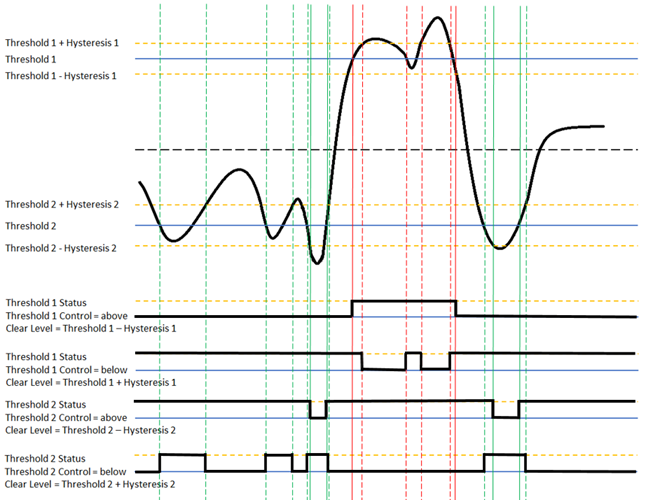 Figure 1. Threshold Programming with Hysteresis
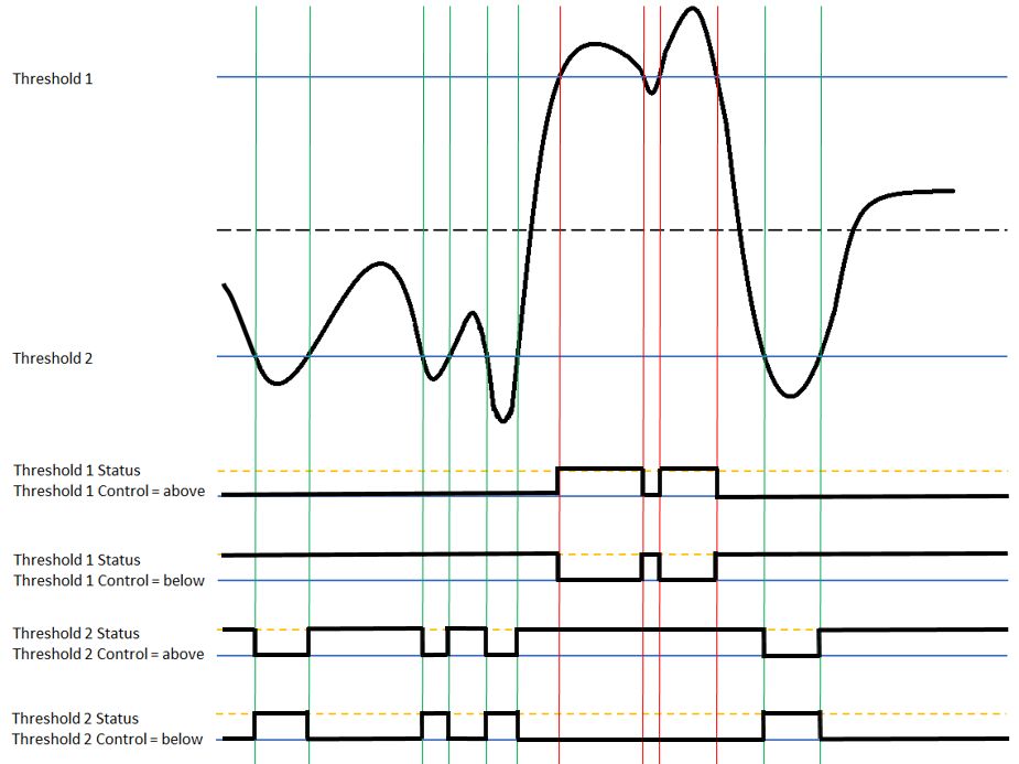 Figure 2. Threshold Programming with No Hysteresis
Saturation Programming
A low and high saturation setting that can be independently programmed on the A/D modules. These saturation values are used to monitor the acquired data and set a status when the specified saturation is reached as well as setting the A/D reading to the saturation value. Saturation programming can be used to prevent the A/D reading from exceeding the saturation value. Refer to Figure 3 for illustrations of Saturation Programming
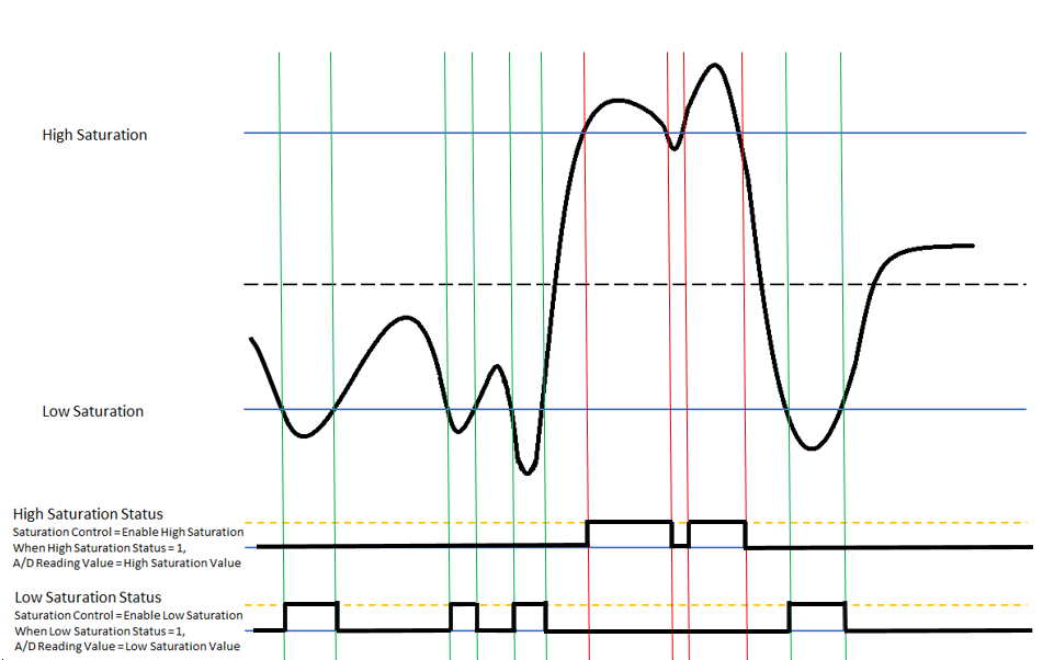 Figure 3. Saturation Programming
REGISTER DESCRIPTIONS
The register descriptions provide the register name, Type, Data Range, Read or Write information, Initialized Value, and a description of the function.
Threshold Detect Programming Registers
There are two threshold and hysteresis registers that can be independently programmed on the A/D modules.
Threshold Detect Level
The Threshold Detect Level registers sets the first and second threshold level values.
| Threshold Detect Level 1 | |
| Function: | Sets the first threshold level value |
| Type: | signed binary word (32-bit) (Integer Mode) or Single Precision Floating Point Value (IEEE-754) (Floating Point Mode) |
| Data Range: | Voltage Threshold Level values are dependent on Polarity and Range settings for the channel. Enable Floating Point Mode: 0 (Integer Mode) ` Unipolar: (AD4-AD6, ADE-ADF) 0x0000 0000 to 0x0000 FFFF ` (AD1-AD3): 0x0000 0000 to 0x00FF FFFF ` Bipolar (2's complement. 24-bit value sign extended to 32 bits): ` (AD4-AD6, ADE-ADF) 0xFFFF 8000 to 0x0000 7FFF; ` (AD1-AD3): 0xFF80 0000 to 0x007F FFFF Enable Floating Point Mode: 1 (Floating Point Mode) ` Single Precision Floating Point Value (IEEE-754) |
| Read/Write: | R/W |
| Initialized Value: | 90% of full scale (bipolar) |
| Threshold Detect Level 2 | |
| Function: | Sets the second threshold level value. |
| Type: | signed binary word (32-bit) (Integer Mode) or Single Precision Floating Point Value (IEEE-754) (Floating Point Mode) |
| Data Range: | Voltage Threshold Level values are dependent on Polarity and Range settings for the channel. Enable Floating Point Mode: 0 (Integer Mode) ` Unipolar: (AD4-AD6, ADE-ADF) 0x0000 0000 to 0x0000 FFFF ` (AD1-AD3): 0x0000 0000 to 0x00FF FFFF ` Bipolar (2's complement. 24-bit value sign extended to 32 bits): ` (AD4-AD6, ADE-ADF) 0xFFFF 8000 to 0x0000 7FFF; ` (AD1-AD3): 0xFF80 0000 to 0x007F FFFF Enable Floating Point Mode: 1 (Floating Point Mode) ` Single Precision Floating Point Value (IEEE-754) |
| Read/Write: | R/W |
| Initialized Value: | -90% of full scale (bipolar) |
Threshold Detect Hysteresis
The Threshold Detect Hysteresis registers sets the first and second threshold hysteresis values. Note, the hysteresis value must be a positive value.
| Threshold Detect Hysteresis 1 | |
| Function: | Sets the first threshold hysteresis value. This value must be positive. |
| Type: | signed binary word (32-bit) or Single Precision Floating Point Value (IEEE-754) (Floating Point Mode) |
| Data Range: | Voltage Threshold Hysteresis values are dependent on Polarity and Range settings for the channel. Enable Floating Point Mode: 0 (Integer Mode) ` Unipolar: (AD4-AD6, ADE-ADF) 0x0000 0000 to 0x0000 FFFF ` (AD1-AD3): 0x0000 0000 to 0x00FF FFFF ` Bipolar (2's complement. 24-bit value sign extended to 32 bits): ` (AD4-AD6, ADE-ADF) 0xFFFF 8000 to 0x0000 7FFF; ` (AD1-AD3): 0xFF80 0000 to 0x007F FFFF Enable Floating Point Mode: 1 (Floating Point Mode) ` Single Precision Floating Point Value (IEEE-754) |
| Read/Write: | R/W |
| Initialized Value: | 0 |
| Threshold Detect Hysteresis 2 | |
| Function: | Sets the second threshold hysteresis value. This value must be positive. |
| Type: | signed binary word (32-bit) or Single Precision Floating Point Value (IEEE-754) (Floating Point Mode) |
| Data Range: | Voltage Threshold Hysteresis values are dependent on Polarity and Range settings for the channel. Enable Floating Point Mode: 0 (Integer Mode) ` Unipolar: (AD4-AD6, ADE-ADF) 0x0000 0000 to 0x0000 FFFF ` (AD1-AD3): 0x0000 0000 to 0x00FF FFFF ` Bipolar (2's complement. 24-bit value sign extended to 32 bits): ` (AD4-AD6, ADE-ADF) 0xFFFF 8000 to 0x0000 7FFF; ` (AD1-AD3): 0xFF80 0000 to 0x007F FFFF Enable Floating Point Mode: 1 (Floating Point Mode) ` Single Precision Floating Point Value (IEEE-754) |
| Read/Write: | R/W |
| Initialized Value: | 0 |
Threshold Detect Control
| Threshold Detect Control | |
| Function: | Sets up detect control for the two thresholds for each channel. |
| Type: | unsigned binary word (32-bit) |
| Data Range: | 0x0000 0000 to 0xFFFF FFFF |
| Read/Write: | R/W |
| Initialized Value: | 0 |
| Operational Settings: | Set bit to 0 to detect above the threshold level. Set bit to 1 to detect below the threshold level. |
| AD1-AD3 | |||||||||||||||
| D31 | D30 | D29 | D28 | D27 | D26 | D25 | D24 | D23 | D22 | D21 | D20 | D19 | D18 | D17 | D16 |
| 0 | 0 | 0 | 0 | 0 | 0 | 0 | 0 | Ch12 | Ch11 | Ch10 | Ch9 | ||||
| T2 | T1 | T2 | T1 | T2 | T1 | T2 | T1 | ||||||||
| D | D | D | D | D | D | D | D | ||||||||
| AD4-AD6 and ADE-ADF | |||||||||||||||
| D31 | D30 | D29 | D28 | D27 | D26 | D25 | D24 | D23 | D22 | D21 | D20 | D19 | D18 | D17 | D16 |
| Ch16 | Ch15 | Ch14 | Ch13 | Ch12 | Ch11 | Ch10 | Ch9 | ||||||||
| T2 | T1 | T2 | T1 | T2 | T1 | T2 | T1 | T2 | T1 | T2 | T1 | T2 | T1 | T2 | T1 |
| D | D | D | D | D | D | D | D | D | D | D | D | D | D | D | D |
| All A/D Modules | |||||||||||||||
| D15 | D14 | D13 | D12 | D11 | D10 | D9 | D8 | D7 | D6 | D5 | D4 | D3 | D2 | D1 | D0 |
| Ch8 | Ch7 | Ch6 | Ch5 | Ch4 | Ch3 | Ch2 | Ch1 | ||||||||
| T2 | T1 | T2 | T1 | T2 | T1 | T2 | T1 | T2 | T1 | T2 | T1 | T2 | T1 | T2 | T1 |
| D | D | D | D | D | D | D | D | D | D | D | D | D | D | D | D |
Saturation Programming Registers
A low and high saturation setting that can be independently programmed on the A/D modules.
Saturation Value
The Low Saturation Value registers sets value to report as A/D reading and sets the Saturation Status bit when the A/D data is below the low saturation value. The High Saturation Value registers sets value to report as A/D reading and sets the Saturation Status bit when the A/D data is above the high saturation value.
| Low Saturation | |
| Function: | Sets the low saturation value. |
| Type: | signed binary word (32-bit) or Single Precision Floating Point Value (IEEE-754) (Floating Point Mode) |
| Data Range: | Saturation Voltage values are dependent on Polarity and Range settings for the channel. Enable Floating Point Mode: 0 (Integer Mode) ` Unipolar: (AD4-AD6, ADE-ADF) 0x0000 0000 to 0x0000 FFFF ` (AD1-AD3): 0x0000 0000 to 0x00FF FFFF ` Bipolar (2's complement. 24-bit value sign extended to 32 bits): ` (AD4-AD6, ADE-ADF) 0xFFFF 8000 to 0x0000 7FFF; ` (AD1-AD3): 0xFF80 0000 to 0x007F FFFF Enable Floating Point Mode: 1 (Floating Point Mode) ` Single Precision Floating Point Value (IEEE-754) |
| Read/Write: | R/W |
| Initialized Value: | 0 |
| High Saturation | |
| Function: | Sets the high saturation value. |
| Type: | signed binary word (32-bit) or Single Precision Floating Point Value (IEEE-754) (Floating Point Mode) |
| Data Range: | Saturation Voltage values are dependent on Polarity and Range settings for the channel. Enable Floating Point Mode: 0 (Integer Mode) ` Unipolar: (AD4-AD6, ADE-ADF) 0x0000 0000 to 0x0000 FFFF ` (AD1-AD3): 0x0000 0000 to 0x00FF FFFF ` Bipolar (2's complement. 24-bit value sign extended to 32 bits): ` (AD4-AD6, ADE-ADF) 0xFFFF 8000 to 0x0000 7FFF; ` (AD1-AD3): 0xFF80 0000 to 0x007F FFFF Enable Floating Point Mode: 1 (Floating Point Mode) ` Single Precision Floating Point Value (IEEE-754) |
| Read/Write: | R/W |
| Initialized Value: | 0 |
| Saturation Control | |
| Function: | Sets up saturation control for the two saturation levels for each channel. |
| Type: | unsigned binary word (32-bit) |
| Data Range: | 0x0000 0000 to 0xFFFF FFFF |
| Read/Write: | R/W |
| Initialized Value: | 0 |
| Operational Settings: | Set bits to 1 to enable Saturation Control. Set bits to 0 to disable Saturation Control. Each channel control consists of two bits: Low Saturation Control ("Even' bits (B0, B2, B4,...)) and High Saturation Control ("Odd' bits (B1, B3, B5,...)). |
| AD1-AD3 | |||||||||||||||
| D31 | D30 | D29 | D28 | D27 | D26 | D25 | D24 | D23 | D22 | D21 | D20 | D19 | D18 | D17 | D16 |
| 0 | 0 | 0 | 0 | 0 | 0 | 0 | 0 | Ch12 | Ch11 | Ch10 | Ch9 | ||||
| High | Low | High | Low | High | Low | High | Low | ||||||||
| D | D | D | D | D | D | D | D | ||||||||
| AD4-AD6 and ADE-ADF | |||||||||||||||
| D31 | D30 | D29 | D28 | D27 | D26 | D25 | D24 | D23 | D22 | D21 | D20 | D19 | D18 | D17 | D16 |
| Ch16 | Ch15 | Ch14 | Ch13 | Ch12 | Ch11 | Ch10 | Ch9 | ||||||||
| High | Low | High | Low | High | Low | High | Low | High | Low | High | Low | High | Low | High | Low |
| D | D | D | D | D | D | D | D | D | D | D | D | D | D | D | D |
| All A/D Modules | |||||||||||||||
| D15 | D14 | D13 | D12 | D11 | D10 | D9 | D8 | D7 | D6 | D5 | D4 | D3 | D2 | D1 | D0 |
| Ch8 | Ch7 | Ch6 | Ch5 | Ch4 | Ch3 | Ch2 | Ch1 | ||||||||
| High | Low | High | Low | High | Low | High | Low | High | Low | High | Low | High | Low | High | Low |
| D | D | D | D | D | D | D | D | D | D | D | D | D | D | D | D |
Status and Interrupt
The A/D Module provides status registers for Threshold Detect and Saturation.
Threshold Detect Status
There are four registers associated with the Threshold Detect Status: Dynamic, Latched, Interrupt Enable, and Set Edge/Level Interrupt.
0 = Normal; 1 = Outside of threshold range. The status is created based on the values set in the Threshold Detect 1 and Threshold Detect 2 registers. Bits D0 and D1 represent if channel 1 is outside the threshold for Threshold Detect 1 and Threshold Detect 2 respectively, Bits D2 and D3 represent if channel 2 is outside the threshold for Threshold Detect 1 and Threshold Detect 2 respectively, etc. This pattern continues for all channels.
| Threshold Detect Status | |
| Function: | Sets the corresponding bit associated with the channel's Threshold Detect error. |
| Type: | unsigned binary word (32-bit) |
| Data Range: | 0x0000 0000 to 0x00FF FFFF |
| Read/Write: | R (Dynamic), R/W (Latched, Interrupt Enable, Edge/Level Interrupt) |
| Initialized Value: | 0 |
| Threshold Detect Dynamic Status | |||||||||||||||
| Threshold Detect Latched Status | |||||||||||||||
| Threshold Detect Interrupt Enable | |||||||||||||||
| Threshold Detect Set Edge/Level Interrupt | |||||||||||||||
| AD1-AD3 | |||||||||||||||
| D31 | D30 | D29 | D28 | D27 | D26 | D25 | D24 | D23 | D22 | D21 | D20 | D19 | D18 | D17 | D16 |
| 0 | 0 | 0 | 0 | 0 | 0 | 0 | 0 | Ch12 | Ch11 | Ch10 | Ch9 | ||||
| T2 | T1 | T2 | T1 | T2 | T1 | T2 | T1 | ||||||||
| D | D | D | D | D | D | D | D | ||||||||
| AD4-AD6 and ADE-ADF | |||||||||||||||
| D31 | D30 | D29 | D28 | D27 | D26 | D25 | D24 | D23 | D22 | D21 | D20 | D19 | D18 | D17 | D16 |
| Ch16 | Ch15 | Ch14 | Ch13 | Ch12 | Ch11 | Ch10 | Ch9 | ||||||||
| T2 | T1 | T2 | T1 | T2 | T1 | T2 | T1 | T2 | T1 | T2 | T1 | T2 | T1 | T2 | T1 |
| D | D | D | D | D | D | D | D | D | D | D | D | D | D | D | D |
| All A/D Modules | |||||||||||||||
| D15 | D14 | D13 | D12 | D11 | D10 | D9 | D8 | D7 | D6 | D5 | D4 | D3 | D2 | D1 | D0 |
| Ch8 | Ch7 | Ch6 | Ch5 | Ch4 | Ch3 | Ch2 | Ch1 | ||||||||
| T2 | T1 | T2 | T1 | T2 | T1 | T2 | T1 | T2 | T1 | T2 | T1 | T2 | T1 | T2 | T1 |
| D | D | D | D | D | D | D | D | D | D | D | D | D | D | D | D |
Saturation Status
There are four registers associated with the Saturation Status: Dynamic, Latched, Interrupt Enable, and Set Edge/Level Interrupt.
0 = Normal; 1 = Outside of saturation range. The status is created based on the values set in the Low Saturation and High Saturation registers. Bits D0 and D1 represent if channel 1 is outside the voltage for Low Saturation and High Saturation respectively, Bits D2 and D3 represent if channel 2 is outside the voltage for Low Saturation and High Saturation respectively, etc. This pattern continues for all channels.
| Saturation Status | |
| Function: | Sets the corresponding bit associated with the channel's Saturation error. |
| Type: | unsigned binary word (32-bit) |
| Data Range: | 0x0000 0000 to 0x00FF FFFF |
| Read/Write: | R (Dynamic), R/W (Latched, Interrupt Enable, Edge/Level Interrupt) |
| Initialized Value: | 0 |
| Saturation Dynamic Status | |||||||||||||||
| Saturation Latched Status | |||||||||||||||
| Saturation Interrupt Enable | |||||||||||||||
| Saturation Set Edge/Level Interrupt | |||||||||||||||
| AD1-AD3 | |||||||||||||||
| D31 | D30 | D29 | D28 | D27 | D26 | D25 | D24 | D23 | D22 | D21 | D20 | D19 | D18 | D17 | D16 |
| 0 | 0 | 0 | 0 | 0 | 0 | 0 | 0 | Ch12 | Ch11 | Ch10 | Ch9 | ||||
| High | Low | High | Low | High | Low | High | Low | ||||||||
| D | D | D | D | D | D | D | D | ||||||||
| AD4-AD6 and ADE-ADF | |||||||||||||||
| D31 | D30 | D29 | D28 | D27 | D26 | D25 | D24 | D23 | D22 | D21 | D20 | D19 | D18 | D17 | D16 |
| Ch16 | Ch15 | Ch14 | Ch13 | Ch12 | Ch11 | Ch10 | Ch9 | ||||||||
| High | Low | High | Low | High | Low | High | Low | High | Low | High | Low | High | Low | High | Low |
| D | D | D | D | D | D | D | D | D | D | D | D | D | D | D | D |
| All A/D Modules | |||||||||||||||
| D15 | D14 | D13 | D12 | D11 | D10 | D9 | D8 | D7 | D6 | D5 | D4 | D3 | D2 | D1 | D0 |
| Ch8 | Ch7 | Ch6 | Ch5 | Ch4 | Ch3 | Ch2 | Ch1 | ||||||||
| High | Low | High | Low | High | Low | High | Low | High | Low | High | Low | High | Low | High | Low |
| D | D | D | D | D | D | D | D | D | D | D | D | D | D | D | D |
FUNCTION REGISTER MAP
KEY
| Configuration/Control |
| State/Measurement/Status |
| THRESHOLD DETECT PROGRAMMING REGISTERS | |||||
| **Data is represented in Floating Point if Enable Floating Point Mode register is set to Floating Point Mode (1). | |||||
| NOTE: Base Address - 0x4000 0000 | |||||
| OFFSET | REGISTER NAME | ACCESS | OFFSET | REGISTER NAME | ACCESS |
| All A/D Modules | |||||
| 0x1980 | Threshold Detect Level 1 Ch 1** | R/W | 0x1A00 | Threshold Detect Level 1 Hysteresis Ch 1** | R/W |
| 0x1984 | Threshold Detect Level 1 Ch 2** | R/W | 0x1A04 | Threshold Detect Level 1 Hysteresis Ch 2** | R/W |
| 0x1988 | Threshold Detect Level 1 Ch 3** | R/W | 0x1A08 | Threshold Detect Level 1 Hysteresis Ch 3** | R/W |
| 0x198C | Threshold Detect Level 1 Ch 4** | R/W | 0x1A0C | Threshold Detect Level 1 Hysteresis Ch 4** | R/W |
| 0x1990 | Threshold Detect Level 1 Ch 5** | R/W | 0x1A10 | Threshold Detect Level 1 Hysteresis Ch 5** | R/W |
| 0x1994 | Threshold Detect Level 1 Ch 6** | R/W | 0x1A14 | Threshold Detect Level 1 Hysteresis Ch 6** | R/W |
| 0x1998 | Threshold Detect Level 1 Ch 7** | R/W | 0x1A18 | Threshold Detect Level 1 Hysteresis Ch 7** | R/W |
| 0x199C | Threshold Detect Level 1 Ch 8** | R/W | 0x1A1C | Threshold Detect Level 1 Hysteresis Ch 8** | R/W |
| 0x19A0 | Threshold Detect Level 1 Ch 9** | R/W | 0x1A20 | Threshold Detect Level 1 Hysteresis Ch 9** | R/W |
| 0x19A4 | Threshold Detect Level 1 Ch 10** | R/W | 0x1A24 | Threshold Detect Level 1 Hysteresis Ch 10** | R/W |
| 0x19A8 | Threshold Detect Level 1 Ch 11** | R/W | 0x1A28 | Threshold Detect Level 1 Hysteresis Ch 11** | R/W |
| 0x19AC | Threshold Detect Level 1 Ch 12** | R/W | 0x1A2C | Threshold Detect Level 1 Hysteresis Ch 12** | R/W |
| AD4-AD6, ADE-ADF | |||||
| 0x19B0 | Threshold Detect Level 1 Ch 13** | R/W | 0x1A30 | Threshold Detect Level 1 Hysteresis Ch 13** | R/W |
| 0x19B4 | Threshold Detect Level 1 Ch 14** | R/W | 0x1A34 | Threshold Detect Level 1 Hysteresis Ch 14** | R/W |
| 0x19B8 | Threshold Detect Level 1 Ch 15** | R/W | 0x1A38 | Threshold Detect Level 1 Hysteresis Ch 15** | R/W |
| 0x19BC | Threshold Detect Level 1 Ch 16** | R/W | 0x1A3C | Threshold Detect Level 1 Hysteresis Ch 16** | R/W |
| All A/D Modules | |||||
| 0x1A80 | Threshold Detect Level 2 Ch 1** | R/W | 0x1B00 | Threshold Detect Level 2 Hysteresis Ch 1** | R/W |
| 0x1A84 | Threshold Detect Level 2 Ch 2** | R/W | 0x1B04 | Threshold Detect Level 2 Hysteresis Ch 2** | R/W |
| 0x1A88 | Threshold Detect Level 2 Ch 3** | R/W | 0x1B08 | Threshold Detect Level 2 Hysteresis Ch 3** | R/W |
| 0x1A8C | Threshold Detect Level 2 Ch 4** | R/W | 0x1B0C | Threshold Detect Level 2 Hysteresis Ch 4** | R/W |
| 0x1A90 | Threshold Detect Level 2 Ch 5** | R/W | 0x1B10 | Threshold Detect Level 2 Hysteresis Ch 5** | R/W |
| 0x1A94 | Threshold Detect Level 2 Ch 6** | R/W | 0x1B14 | Threshold Detect Level 2 Hysteresis Ch 6** | R/W |
| 0x1A98 | Threshold Detect Level 2 Ch 7** | R/W | 0x1B18 | Threshold Detect Level 2 Hysteresis Ch 7** | R/W |
| 0x1A9C | Threshold Detect Level 2 Ch 8** | R/W | 0x1B1C | Threshold Detect Level 2 Hysteresis Ch 8** | R/W |
| 0x1AA0 | Threshold Detect Level 2 Ch 9** | R/W | 0x1B20 | Threshold Detect Level 2 Hysteresis Ch 9** | R/W |
| 0x1AA4 | Threshold Detect Level 2 Ch 10** | R/W | 0x1B24 | Threshold Detect Level 2 Hysteresis Ch 10** | R/W |
| 0x1AA8 | Threshold Detect Level 2 Ch 11** | R/W | 0x1B28 | Threshold Detect Level 2 Hysteresis Ch 11** | R/W |
| 0x1AAC | Threshold Detect Level 2 Ch 12** | R/W | 0x1B2C | Threshold Detect Level 2 Hysteresis Ch 12** | R/W |
| AD4-AD6, ADE-ADF | |||||
| 0x1AB0 | Threshold Detect Level 2 Ch 13** | R/W | 0x1B30 | Threshold Detect Level 2 Hysteresis Ch 13** | R/W |
| 0x1AB4 | Threshold Detect Level 2 Ch 14** | R/W | 0x1B34 | Threshold Detect Level 2 Hysteresis Ch 14** | R/W |
| 0x1AB8 | Threshold Detect Level 2 Ch 15** | R/W | 0x1B38 | Threshold Detect Level 2 Hysteresis Ch 15** | R/W |
| 0x1ABC | Threshold Detect Level 2 Ch 16** | R/W | 0x1B3C | Threshold Detect Level 2 Hysteresis Ch 16** | R/W |
| 0x1C80 | Threshold Detect Control | R/W | |||
| SATURATION PROGRAMMING REGISTERS | |||||
| **Data is represented in Floating Point if Enable Floating Point Mode register is set to Floating Point Mode (1). | |||||
| NOTE: Base Address - 0x4000 0000 | |||||
| OFFSET | REGISTER NAME | ACCESS | OFFSET | REGISTER NAME | ACCESS |
| All A/D Modules | |||||
| 0x1B80 | Low Saturation Value Ch 1** | R/W | 0x1C00 | High Saturation Value Ch 1** | R/W |
| 0x1B84 | Low Saturation Value Ch 2** | R/W | 0x1C04 | High Saturation Value Ch 2** | R/W |
| 0x1B88 | Low Saturation Value Ch 3** | R/W | 0x1C08 | High Saturation Value Ch 3** | R/W |
| 0x1B8C | Low Saturation Value Ch 4** | R/W | 0x1C0C | High Saturation Value Ch 4** | R/W |
| 0x1B90 | Low Saturation Value Ch 5** | R/W | 0x1C10 | High Saturation Value Ch 5** | R/W |
| 0x1B94 | Low Saturation Value Ch 6** | R/W | 0x1C14 | High Saturation Value Ch 6** | R/W |
| 0x1B98 | Low Saturation Value Ch 7** | R/W | 0x1C18 | High Saturation Value Ch 7** | R/W |
| 0x1B9C | Low Saturation Value Ch 8** | R/W | 0x1C1C | High Saturation Value Ch 8** | R/W |
| 0x1BA0 | Low Saturation Value Ch 9** | R/W | 0x1C20 | High Saturation Value Ch 9** | R/W |
| 0x1BA4 | Low Saturation Value Ch 10** | R/W | 0x1C24 | High Saturation Value Ch 10** | R/W |
| 0x1BA8 | Low Saturation Value Ch 11** | R/W | 0x1C28 | High Saturation Value Ch 11** | R/W |
| 0x1BAC | Low Saturation Value Ch 12** | R/W | 0x1C2C | High Saturation Value Ch 12** | R/W |
| AD4-AD6, ADE-ADF | |||||
| 0x1BB0 | Low Saturation Value Ch 13** | R/W | 0x1C30 | High Saturation Value Ch 13** | R/W |
| 0x1BB4 | Low Saturation Value Ch 14** | R/W | 0x1C34 | High Saturation Value Ch 14** | R/W |
| 0x1BB8 | Low Saturation Value Ch 15** | R/W | 0x1C38 | High Saturation Value Ch 15** | R/W |
| 0x1BBC | Low Saturation Value Ch 16** | R/W | 0x1C3C | High Saturation Value Ch 16** | R/W |
| 0x1C90 | Saturation Control | R/W | |||
| STATUS REGISTERS | |||||
| *When an event is detected, the bit associated with the event is set in this register and will remain set until the user clears the event bit. Clearing the bit requires writing a 1 back to the specific bit that was set when read (i.e., write-1-to-clear, writing a “1” to a bit set to “1” will set the bit to “0). | |||||
| NOTE: Base Address - 0x4000 0000 | |||||
| OFFSET | REGISTER NAME | ACCESS | OFFSET | REGISTER NAME | ACCESS |
| Threshold | Saturation | ||||
| 0x0940 | Dynamic Status | R | 0x0960 | Dynamic Status | R |
| 0x0944 | Latched Status* | R/W | 0x0964 | Latched Status* | R/W |
| 0x0948 | Interrupt Enable | R/W | 0x0968 | Interrupt Enable | R/W |
| 0x094C | Set Edge/Level Interrupt | R/W | 0x096C | Set Edge/Level Interrupt | R/W |
| INTERRUPT REGISTERS | |||||
| The Interrupt Vector and Interrupt Steering registers are located on the Motherboard Memory Space and do not require any Module Address Offsets. These registers are accessed using the absolute addresses listed in the table below. | |||||
| OFFSET | REGISTER NAME | ACCESS | OFFSET | REGISTER NAME | ACCESS |
| 0x0550 | Module 1 Interrupt Vector 21 - Threshold Status | R/W | 0x0650 | Module 1 Interrupt Steering 21 - Threshold Status | R/W |
| 0x0558 | Module 1 Interrupt Vector 23 - Saturation Status | R/W | 0x0658 | Module 1 Interrupt Steering 23 - Saturation Status | R/W |
| 0x0750 | Module 2 Interrupt Vector 21 - Threshold Status | R/W | 0x0850 | Module 2 Interrupt Steering 21 - Threshold Status | R/W |
| 0x0758 | Module 2 Interrupt Vector 23 - Saturation Status | R/W | 0x0858 | Module 2 Interrupt Steering 23 - Saturation Status | R/W |
| 0x0950 | Module 3 Interrupt Vector 21 - Threshold Status | R/W | 0x0A50 | Module 3 Interrupt Steering 21 - Threshold Status | R/W |
| 0x0958 | Module 3 Interrupt Vector 23 - Saturation Status | R/W | 0x0A58 | Module 3 Interrupt Steering 23 - Saturation Status | R/W |
| 0x0B50 | Module 4 Interrupt Vector 21 - Threshold Status | R/W | 0x0C50 | Module 4 Interrupt Steering 21 - Threshold Status | R/W |
| 0x0B58 | Module 4 Interrupt Vector 23 - Saturation Status | R/W | 0x0C58 | Module 4 Interrupt Steering 23 - Saturation Status | R/W |
| 0x0D50 | Module 5 Interrupt Vector 21 - Threshold Status | R/W | 0x0E50 | Module 5 Interrupt Steering 21 - Threshold Status | R/W |
| 0x0D58 | Module 5 Interrupt Vector 23 - Saturation Status | R/W | 0x0E58 | Module 5 Interrupt Steering 23 - Saturation Status | R/W |
| 0x0F50 | Module 6 Interrupt Vector 21 - Threshold Status | R/W | 0x1050 | Module 6 Interrupt Steering 21 - Threshold Status | R/W |
| 0x0F58 | Module 6 Interrupt Vector 23 - Saturation Status | R/W | 0x1058 | Module 6 Interrupt Steering 23 - Saturation Status | R/W |
REVISION HISTORY
| Module Manual - AD Threshold and Saturation Programming Revision History | ||
| Revision | Revision Date | Description |
| C | 2021-11-30 | C08896; Transition manual to docbuilder format - no technical information change. |
| C1 | 2022-03-16 | C09163, pg.15-17, changed "AD4-AD4" to "AD4-AD6". |
| C2 | 2023-01-24 | ECO C010010, pg.8-9/11, added 24-bit integer mode data ranges. |
| C3 | 2023-06-20 | ECO C10476, removed all ADG module references from manual. |
| C4 | 2024-04-18 | ECO C11441, spelling correction ('2's compliment' to '2's complement); no technical info change. |
DOCS.NAII REVISIONS
| Revision Date | Description |
|---|---|
| 2026-05-18 | Formatting updates throughout manual (non-technical changes). |