DATA SHEET
Click here for the SIU34S data sheet
INTRODUCTION
North Atlantic Industries’ (NAI) Sensor Interface Unit (SIU34S) is a rugged base-plate conduction-cooled chassis that leverages and integrates NAI’s Configurable Open Systems Architecture™ (COSA ®) rugged conduction-cooled 3U OpenVPX SBC, multi-function I/O boards and power supply products. The SIU34S provides a compact, high density, processing & graphics capable data distribution system solution for I/O intensive, mission or control systems applications. The SIU34S supports board-level processing and full I/O control and communication over Ethernet. With local processing, MIL-STD-1553, ARINC 429/575, Serial or ARINC 825 CAN bus are also available as primary communications interfaces when the boards are configured as such. PowerPC, Intel® or ARM Single Board Computer (SBC) processors can be added for a complete processing and I/O solution. The SIU34S is designed to support up to four NAI multi-function pre-configurable SBC/multifunction I/O boards, with or without processing, that support a wide variety of interface and communications smart function modules, all fitted/housed in a single rugged multi-board slot SIU system chassis, which is “delivered” pre-integrated and fully tested as a system.
OBJECTIVES
This manual provides the user with basic hardware implementation and information regarding the operation and interface of the SIU34S. Each SIU34S is fitted with either up to four 3U OpenVPX boards and a single mil-standard power supply unit. Additional PSU option for “hold-up” power/time is available.
SCOPE
This manual only covers the operation of the SIU34S as a stand-alone I/O subsystem. This manual does not cover specific details relating to the operation of the specific I/O boards and function module fitted within the SIU34S. Please reference the board specific documentation for details regarding the board level configuration(s).
CONVENTIONS USED IN THIS MANUAL
WARNINGS, CAUTIONS, and NOTES


Note
An operating procedure, practice, or condition, etc., that is essential to emphasize. All numbers are expressed in decimal format unless otherwise noted.
GENERAL SAFETY NOTICES
The following general safety notices supplement the specific warnings and cautions appearing elsewhere in the manual. They are recommended precautions that must be understood and applied during operation and maintenance of the instrument covered herein.
Serious injury may result if personnel fail to observe safety precautions. Dependent on configuration, some modules (e.g. Synchro / Resolver or AC signal sources) can generate output signals with high voltages. Be careful not to contact high-voltage connections when installing, operating or maintaining this instrument.

The SIU34S is delivered as a standalone system with no accessible or serviceable parts.
REPAIR
DO NOT ATTEMPT REPAIR. Under no circumstances should repair of this instrument be attempted. All repairs to this chassis must be accomplished at the factory.
HIGH VOLTAGE
 HIGH VOLTAGE may be used in the operation of this equipment.
INPUT POWER ALWAYS ON

Note
The design of the model SIU34S is such that input power is continuously supplied to internal circuits when connected to a main power source. To disconnect the SIU34S from external power, the external power source should first be de-energized. The power input cable can then be disconnected.
Website https://www.naii.com/
SYSTEM SPECIFICATIONS AND DETAILS
Introduction
The model SIU34S is a next generation rugged systems chassis joining the NAI Sensor Interface Unit (SIU) system chassis family pedigree. The SIU34S is configured to support a wide variety of SBC and multifunction I/O boards that can be configured to support a variety of processing, communications and I/O functions that are supported under the NAI Configurable Open Systems Architecture™ (COSA®) product families.
The SIU34S can function either as a centralized or distributed system. It can also be used to supplement existing legacy systems by easily adding sensor data acquisition as well as general I/O and communication interfaces without expensive legacy chassis and backplane redesign. It has been designed with rugged embedded industrial, military and aerospace applications in mind.
Leveraging NAI’s field-proven, unique modular architecture, the SIU34S supports standard 3U OpenVPX board-level compatible boards that can be fitted with a wide selection of different Intelligent I/O, motion simulation/measurement and communications functions such as:
| A/D Converter | D/A Converter | I/O TTL/CMOS | RTD | I/O Discrete |
| I/O Differential Transceiver | Synchro/Resolver LVDT/RVDT Measurement | Synchro/Resolver LVDT/RVDT Simulation | Strain Gauge | Encoder |
| Dual-Channel Dual Redundant BC/RT/MT MIL-STD-1553 | High-Speed Sync/Async RS232/422/423/485 | ARINC 429/575 | CAN Bus | I/O Relay |
| AC Reference | Ethernet Switch | SSD/Flash | Check w/ NAI's factory or website for latest selection of available functions | |
This approach provides unprecedented flexibility for supporting existing or new applications where there are specific interfacing requirements.
Significant application benefits include:
- Independent (pre-processed) I/O functionality targeted to specific data acquisition/control areas
- Additional capabilities, technology insertion and sensor interfacing to existing fielded applications
- Minimal integration risk based on current field-proven, deployed technologies
Specifications
The SIU34S is designed to meet the following general product specifications and is provided as a reference. Actual configuration and usage may affect size, weight, and power (SWaP) specifications. Please contact NAI for discerning/defining SWaP considerations regarding specific program configurations. See additional details herein.
General
SIU34S General SWaP Specifications
| Input Voltage | Standard/Default: DC: 18 to 36 VDC (28 VDC nominal) |
|---|---|
| Power (Base unit): | ~10 W (PSU efficiency, at 100W load) @ 28 VDC nominal Then, add the power calculated for the configuration-specific board’s module(s) power (see separate specific boards and module(s) specifications). I/O Signal GND reference is isolated from main power source return and chassis. |
| Power/Heat Dissipation: | Conduction Cooled (CC): ~125 watts (maximum) when properly mounted to a cold plate, which must be maintained at a temperature not to exceed 71°C. Air/Convection Cooled (AC) Contact/consult with NAI for configuration and power dissipation. SIU Air/Convection version maximum power dissipation is dependent, but not limited to, configuration, power dissipation, air flow, program and other environmental considerations. NOTE: The total SIU34S power dissipation is dependent on the configuration of the boards and function module types fitted in the SIU34S. Environmental and other operating characteristic variable considerations should be considered. |
| Temperature, Operating: | -40°C to 71°C Conduction cooled: As measured at primary thermal transfer interface. |
| Temperature, Storage: | -55°C to 105°C |
| Size: | Height: ~5.1” (130 mm) CC / ~7.2” (183 mm) AC (w/additional heat dissipator fin height) Depth: ~9.5” (241 mm) Width: ~7.8” (198 mm) CC or ~6.0” (152 mm) AC |
| Weight: | The weight of an SIU34S system is dependent on the configuration. The approximate weight of the SIU34S is based on the selection of the PSU, boards and functional module(s). The approximate weight of a configured SIU34S is: ~9.2 lbs. unpopulated - Chassis/backplane/rigid flex & connector boards/PSU (conduction cooled) (includes ~2.2 lbs. for PSU) ~9.7 lbs. unpopulated - Chassis/backplane/rigid flex & connector boards/PSU (air/convection cooled) (includes ~2.2 lbs. for PSU) ~14.6 lbs. fully populated (conduction cooled) (includes ~1.35 lbs. for each additional fully function module populated board) ~15.1 lbs. fully populated (air/convection cooled) (includes ~1.35 lbs. for each additional fully function module populated board) |
UNPACKING AND INSPECTION
Unpacking
The SIU34S packing materials were designed specifically for transport protection of the SIU34S. When receiving the shipment container, inspect packaging for any evidence of physical damage. If damage is evident, it is recommended that the carrier agent is present when opening the shipping container. It is further recommended that all packing material is retained in the event the SIU34S needs to be shipped elsewhere.
System/Chassis Identification
An identification label, indicating part number, unique serial number and Ethernet PHY MACs / default IP address(es) is affixed to the system chassis.
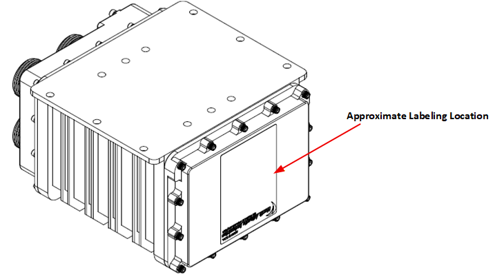
Figure 1. SIU34S Unit Identification Label Location
Label information provided
- Unit Level Part Number Unit
- Level Serial Number Unit
- Level Date Code
Also, typically provided with:
- Slot/Board configuration(s) as applicable
- Slot/Board serial numbers and D/C
- Slot/Board IP address / MAC address (if applicable)
Special labeling requirements are also considered (i.e. UID matrix, customer part number, etc.). Contact factory for special labeling requirements.
Inspection
Inspect the chassis and connectors to ensure that they were not damaged during transit.
MECHANICAL INTERFACE
Mechanical Description
The standard SIU34S is a rugged milled 6061 aerospace grade aluminum alloy stock. The conduction cooled version is expected to be mounted to a thermally conductive surface to maintain the specified temperature. The system thermal management design considerations should ensure that the chassis thermal interface (SIU34S bottom surface) does not exceed 71°C. Mounting holes are provided on the chassis bottom housing flanges (as depicted).
Maximum power and heat dissipation are dependent on the board and function complement chosen. Contact NAI for application guidance. See the reference outline drawing(s) below.
Mounting Requirements
The SIU34S is conduction cooled and must be mounted in accordance with the drawing. The Outline and Installation Drawing (OID) provides recommended hardware, torque, cold-plate flatness and surface finish specifications, and thermal conductivity requirements.
_manua_edits.pdf_OID_1_cropped.png)
Figure 2. SIU34S Conduction Cooled Outline Dimensions & Mounting Pattern (Reference Only)
Notes:
- For reference only.
- Unless otherwise specified, dimensions are in inches (mm); tolerances are:
- 2 PL DEC ±0.01; 3 PL DEC ±0.005
- FRACT ±1/64 (0.4); ANGLES ±1/2 (12.7)
_manua_edits.pdf_OID_2_cropped.PNG)
Figure 3. SIU34S Conduction Cooled w/Fiber Optic Option Outline Dimensions & Mounting Pattern (Reference Only)
Notes:
- For reference only.
- Unless otherwise specified, dimensions are in inches (mm); tolerances are:
- 2 PL DEC ±0.01; 3 PL DEC ±0.005
- FRACT ±1/64 (0.4); ANGLES ±1/2 (12.7)
Chassis (Earth) GND
Chassis ground point threaded insert location is on the connector face (front) of the SIU34S as shown.
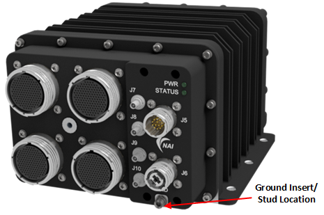
Figure 4. SIU34S Outline Dimensions/Chassis GND location
Note:
A Chassis GND braid or equivalent is expected to be secured by the following hardware or equivalent (delivered/installed with the SIU34S assembly):
- SCREW, SOCKET HEAD CAP, 8-32, ½” LONG, 18-8 SS
- Lock Washer, #8, 0.174” ID, 0.293” OD, 18-8 SS
- Flat Washer, #8, 0.172” ID, 0.375” OD, 18-8 SS
Securing information:
- The chassis is designed/built with a helical insert: NAS1130-08-15 or equivalent (8-32 Helical Insert, 0.246” Length, 18-8 Stainless Steel)
- Maximum screw/insert hole depth is 0.4”
- Recommended torque for the SIU34S Chassis GND screw: 15 in-lbs. (170 N-cm)
Finish
Unless otherwise specified, the following standard finish, or equivalent per NAI process requirements applies:
- PRE-TREATMENT: CHEMICAL FILM COATING IAW MIL-DTL-5541, TYPE II, CLASS 3, ALL OVER.
- PAINT PRIMER COAT: IAW-MIL-DTL-53022F, TYPE IV, CLASS L, WITH A 0.9MIL MINIMUM DRY FILM THICKNESS TO EXTERIOR SURFACES SHOWN IN PAINT MASKING FIGURES.
- PAINT FINISH COAT: APPLY MEDIUM TEXTURE USING PER MIL-PRF-85285, TYPE I, CLASS 2, SEMI-GLOSS BLACK WITH A DRY FILM THICKNESS OF 0.0008 TO 0.0012 TO EXTERIOR SURFACES.
- FINISH NOTES 2 AND 3 OMITTED FROM THERMAL INTERFACE SURFACE INDICATED & FROM ALL HARDWARE.
CONNECTOR DESIGNATIONS, LOCATIONS & DESCRIPTIONS
The Power, I/O Interface and Ethernet connectors are located on the SIU34S front panel housing.
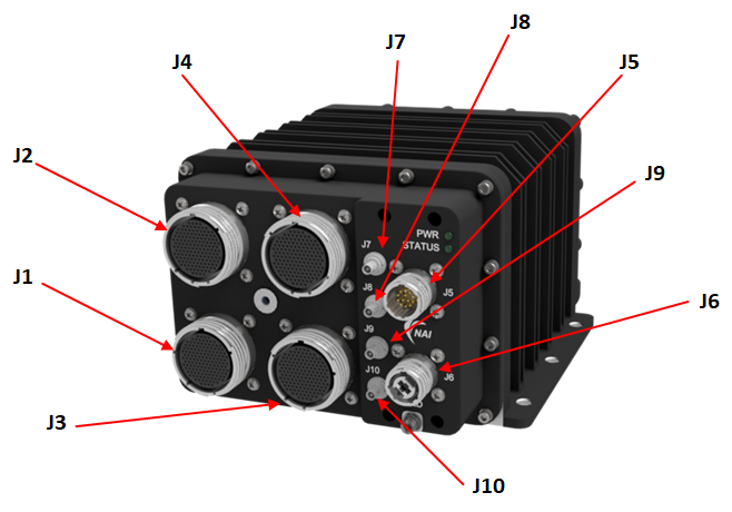
Figure 5. SIU34S (Front Panel Connector Placement)
SIU34S Connector Designation and Description
| REF. DES. | KEY | MANUFACTURER / MIL-DTL SPEC. (or Equiv.) | P/N | MATE P/N |
|---|---|---|---|---|
| J1 | N | AMPHENOL | TVP02RF-23-151S(S2AD) | TV06RF-23-151P |
| J2 | A | AMPHENOL | TVP02RF-23-151SA(S2AD) | TV06RF-23-151PA |
| J3 | D | AMPHENOL | TVP02RF-23-151SD(S2AD) | TV06RF-23-151PD |
| J4 | B | AMPHENOL | TVP02RF-23-151SB(S2AD) | TV06RF-23-151PB |
| J5 | A | MIL-DTL-D38999 Type | D38999/20FB35PA | D38999/26FB35SA |
| J6 (Option) | N | AMPHENOL | CF-594011-01S w/ MALE MT 12 FIBER FERRULE | CF-594611-01P w/ FEMALE MT 12 FIBER FIRRULE |
| J7 (Option) | AMPHENOL | HD-BNC JACK (75 OHM) | HD-BNC JACK (75 OHM) | |
| J8 (Option) | AMPHENOL | HD-BNC JACK (75 OHM) | HD-BNC JACK (75 OHM) | |
| J9 (Option) | AMPHENOL | HD-BNC JACK (75 OHM) | HD-BNC JACK (75 OHM) | |
| J10 (Option) | AMPHENOL | HD-BNC JACK (75 OHM) | HD-BNC JACK (75 OHM) |
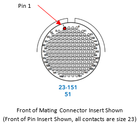
CONNECTOR DETAILS AND PINOUTS
Generic pinout. See module I/O section or contact factory regarding any special module I/O configuration.
J5, Primary Power Connector
Primary input power is supported on the SIU34S via the J5 connector. Power input for the SIU34S: 28 VDC (standard, default).
28 VDC Input Connector
Part Number: D38999/20FB35PA, (w/ 10,000 pf conn filtering)
Shell size 11-35 (Insert 35), “A” key, 13 pins.
Input Mating Connector: D38999/26WB35SA or equivalent
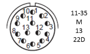 Figure 6. 28 VDC Pin Insert Arrangement, Front View
.28 VDC Pin-out
| J5 Pin | SIU34S Power Input |
| 1, 2, 10, 11 | 28V-PRI |
| 6, 7, 8, 13 | 28V-SEC |
| 3, 4, 5, 12 | 28V-RTN |
| 9 | Chassis GND |
| Each pin is rated at 3 A (max.). | |
I/O Connectors (J1 to J4) and SLOT Designations
Connectors J1 through J4 route all the I/O from the four OpenVPX boards within the SIU34S. The I/O pins from the boards (user defined, and factory configured) are designated from the 3U board slot locations. The Slot-X P1 and P2 connectors of the OpenVPX cards are routed through the backplane to the SIU34S front panel connector rigid-flex assemblies. The specific I/O pin-out information for the J1 through J4 is defined by the configuration of the OpenVPX boards and function modules fitted to the OpenVPX boards.
Unless otherwise specified: MIL-DTL-38999 HD Type III or Equiv. / Electroless Nickel
| Jx Designation | SIU34S Connector MFG. P/N + (or equivalent) | Board # | NAI Conn P/N |
|---|---|---|---|
| J1 | TVP02RF-23-151S(S2AD) | Slot-1 | 05-0473-COM |
| J2 | TVP02RF-23-151SA(S2AD) | Slot-2 | 05-0468-COM |
| J3 | TVP02RF-23-151SD(S2AD) | Slot-3 | 05-0477-COM |
| J4 | TVP02RF-23-151SB(S2AD) | Slot-4 | 05-0469-COM |
| (J5) | (D38999/20FB35PA) | [ PSU (Slot-5) ] | (05-0662-COM) |
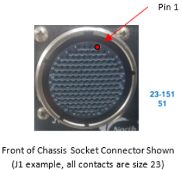
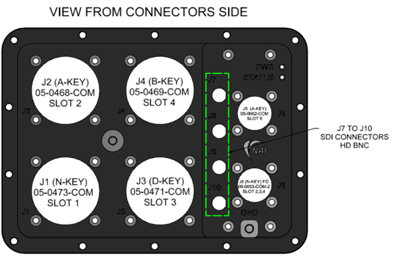
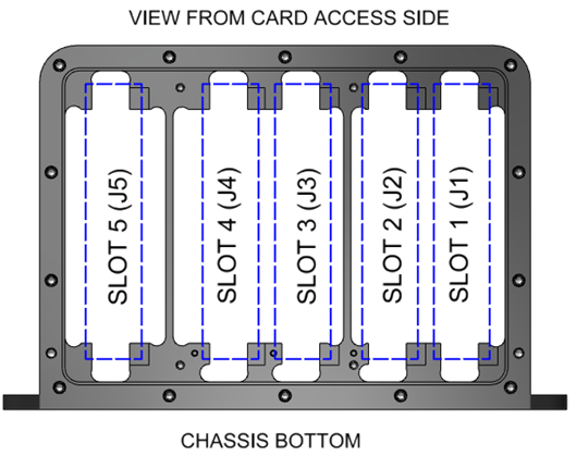
Figure 7. SIU34S Slot and Connector Association Details
Mating Connector Information
Mating Connector Kit; NAI P/N: SIU34S-CONN-KIT
Available as an optional separate line item. The mating connector kit includes 1 each (or equivalent): MIL-DTL-38999 HD Type III or Equiv.
| J1 Mate | NAI P/N: 05-0480-COM |
| HD38999 Type III / TV06RF23-151PN / EN, 151-pin, N-Key | |
| J2 Mate | NAI P/N : 05-0475-COM |
| HD38999 Type III / TV06RF23-151PA / EN, 151-pin, A-Key | |
| J3 Mate | NAI P/N: 05-0478-COM |
| HD38999 Type III / TV06RF23-151PD / EN, 151-pin, D-Key | |
| J4 Mate | NAI P/N : 05-0476-COM |
| HD38999 Type III / TV06RF23-151PB / EN, 151-pin, B-Key | |
| J5 Mate | NAI P/N : 05-0671-COM |
| D38999/26WB35SA / OD, 13-pin, A-Key | |
| J6 Mate (Option) | NAI P/N : 05-0529-COM |
| CONN, MT38999, CIRCULAR, FIBER OPTIC, 11-01, N-Key | |
| J7 - J10 Mate (Option) | NAI P/N : 07-0148 |
| Cable Assembly, BNC Plug to HD-BNC Plug, 75 OHM, Belden 4855R, 78.7" |
POWER-UP AND BASIC OPERATIONS
Panel LEDs & Functions
Front Panel Power & Status LED Indicators
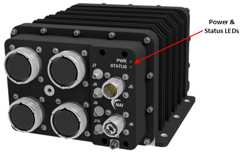
Figure 8. SIU34S Status LEDs Location
SIU34S Status LEDs Function
| LED | STATUS / FUNCTION | |
| ILLUMINATED | EXTINGUISHED | |
| POWER GRN: | Blinking: Initializing Steady On: Power-On/Ready | Power-off |
| *STATUS RED: | Module BIT (Attention required) | No Module BIT Attention Required |
*Status LED operations: Unless otherwise specified, default Status LED operations is controlled by the Slot-1 SBC/Root Complex card over the internal I2C communications link and functionally defined by the customer applied software application (the register is 0x38).
Elapsed Time Counter (ETC)
Integrated within the SIU34S backplane is an Elapsed Time Counter (ETC) IC, which records the accumulated time that the elapsed time recorder’s Event pin has been held high (in 250 ms increments). The ETC is read by the Slot-1 SBC/Root Complex card over the internal I2C communications link (the register is 0x6B).
Basic Operations
The SIU34S is delivered as a tested unit. All pins and operation have been verified. It is recommended that Power and Ethernet connections be made to verify operation of the boards fitted within the SIU34S by making use of NAI’s Embedded Soft Panel based GUI sample application that can be utilized as a board level “exercising” tool (if the SIU34S card configuration supports). The example process below describes the use of NAI’s Ethernet communications software tool.
After applying appropriate power to the SIU34S, connect a host computer (laptop or similar running Windows or Linux), to the appropriate Ethernet enabled/configured board (configured/populated in slot 1) Port A or Port B. The selection of Ethernet Port A or B is dependent on Slot-1 OpenVPX board configuration.
Note
Ethernet port assignments, MAC address, and factory default IP address are indicated on the chassis label.
QUALIFICATION
The SIU34S has been designed to meet the following general specifications. Cooling type, size, weight, power and environmental characteristics may affect the program requirements and the specifications as applied. Contact factory for the SIU34S Qualification Test status.
Environmental
Environmental Qualification Testing Specifications
| *Environmental MIL-STD-810 (1) (unless otherwise specified) | ||||||
| No. | Description | Procedure | Cycles | Table | Figure | Comments |
| 514 | Random Vibe | Method 514.6, 0.1g2/Hz from 100 to 1K Hz., -3dB octave 5-100 Hz and -6dB 1K-2K Hz,(operational) | ||||
| 514 | Sinusoidal Vibe | TBD | ||||
| 501 | Temp (High) | 3 | 3 periods (@ 4 hrs. ea.) within 24 hrs. cycle at 71 ºC baseplate | |||
| 502 | Temp (Low) | 1 | 3 periods (@ 4 hrs. ea.) within 24 hrs. cycle at -40 ºC baseplate | |||
| 503 | Temp (Shock) | 3 | 3 x 1 hr. each hot & cold cycle | |||
| 507 | Humidity | II | 10 | 507.5-7 | 507.5-IX | Cyclic high humidity (Cycle B2) |
| 500 | Altitude (50K) | II | 1 | n/a | n/a | 10m/s to 50,000ft for 1 hr. |
| 513 | Acceleration | II | 1 | 513.6-II | n/a | Carrier-based Aircraft (18g's max) |
| 516 | Shock - Operating | I | 3 | 516.6-I | n/a | 40g's, 1 min each x 6 axis |
| 516 | Shock - Crash | V | 3 | 516.6-I | n/a | 75g's, 1 min each x 6 axis |
| *Ingress Protection IEC 60529 (*1, 2) | ||||||
| No. | Description | Procedure | Cycles | Table | Figure | Comments |
| IP54 | Dust Protection | (other - pending characterization / contact factory) | ||||
| IP54 | Water Splashing | (other - pending characterization / contact factory) | ||||
| IP65 | Dust Tight | (other - pending characterization / contact factory) | ||||
| IP65 | Water Jets | (other - pending characterization / contact factory) | ||||
EMI/EMC Specifications
EMI/EMC Qualification Testing Specifications
| *EMC / MIL-STD-461 (*1, 2) (unless otherwise specified) | ||
| MIL-STD-461F | Method/Curve/Procedure | Comments |
| CE102 | Conducted, Emissions, Power Leads, 10K - 10M Hz | |
| CS101 | Conducted, Susceptibility, Power Leads, 30 - 150K Hz | |
| CS106 | Conducted, Susceptibility, Power Leads | |
| CS114 | Conducted, Susceptibility, Power Leads, 10K - 10M Hz | |
| CS115 | Conducted, Susceptibility, Bulk Injection | |
| CS116 | Conducted, Susceptibility, SIN Transient 10K - 100M Hz | |
| RE101 | Radiated, Emissions, Magnetic Field, 30 - 100K Hz | |
| RE102 | Radiated, Emissions, Electric Field, 10K - 1.25G Hz | |
| RS101 | Radiated, Susceptibility, Magnetic Field, 30 - 100K Hz | |
| RS103 | Radiated, Susceptibility, Electric Field, 2M - 18G Hz | |
Notes:
*1 - Designed to meet / Generic Test Reports Available
*2 - Utilizing proper shielded cables and system grounding practices
HEAT DISSIPATION
The SIU34S is capable of dissipating up to a total of 125 Watts when properly mounted. Generally, the conduction cooled version thermal interface must be maintained at a temperature not to exceed 71°C. Other operating and environmental factors and variable must be considered when specifying for a higher-level system platform integration. The total SIU34S power dissipation is dependent on the configuration of the OpenVPX boards and power supply fitted in the SIU34S.
RELIABILITY
The reliability of the SIU34S is dependent on the configuration of the OpenVPX boards and power supply fitted within it. The Mean Time between Failures is for the SIU34S configured with chassis, backplane, EMI Filter and connectors.
MTBF
The Mean Time between Failures is configuration, environment, and temperature dependent. Please contact factory regarding calculations based on the specific configuration and program requirements.
SIGNAL PIN-OUTS
The following pinout tables provide a general use guideline AS AN EXAMPLE, ONLY. Pinout routing will be dependent on card type/configuration for optimal I/O usage. Consult NAI factory for assistance in determining specific configuration signal definitions as applicable.
Pin-Out / General / I/O Connector (Slot 1)
The following pinout is AN EXAMPLE of a SIU34S Slot-1 populated with a 68INT6-N SBC fitted with a SC3 (8-Channel RS-232/422/485 serial communication) function module and a DT1 (24-Channel discrete input/output) function module.
| J1-MIL Connector | MB - as Configured | MOD-1 / SC3 | MOD-2 / DT1 | Signal Description |
| 1 | MB_P2_TP2P | 10/100/1000BASE-T, ± 2.5V typ. (over twisted pair) | ||
| 2 | MB_P2_TP2N | 10/100/1000BASE-T, ± 2.5V typ. (over twisted pair) | ||
| 3 | MB_P2_TP3P | 10/100/1000BASE-T, ± 2.5V typ. (over twisted pair) | ||
| 4 | MB_P2_TP3N | 10/100/1000BASE-T, ± 2.5V typ. (over twisted pair) | ||
| 5 | ||||
| 6 | ||||
| 7 | MOD2_DATIO06 | DT-IO-GND | 24 CH. Discrete I/O, 0-60 VDC Input/Output, Max Iout 500mA - 2 A, Source/Sink (out) | |
| 8 | MOD2_DATIO11 | VCC2 (7-12) | 24 CH. Discrete I/O, 0-60 VDC Input/Output, Max Iout 500mA - 2 A, Source/Sink (out) | |
| 9 | MOD2_DATIO12 | DT-IO-GND | 24 CH. Discrete I/O, 0-60 VDC Input/Output, Max Iout 500mA - 2 A, Source/Sink (out) | |
| 10 | USB1_SSRXP | USB1-SSRXP | ||
| 11 | USB1_SSRXN | USB1-SSRXP | ||
| 12 | MOD2_DATIO04 | IO-CH04 | 24 CH. Discrete I/O, 0-60 VDC Input/Output, Max Iout 500mA - 2 A, Source/Sink (out) | |
| 13 | MOD2_DATIO03 | IO-CH03 | 24 CH. Discrete I/O, 0-60 VDC Input/Output, Max Iout 500mA - 2 A, Source/Sink (out) | |
| 14 | TTL_CH1 | |||
| 15 | TTL_CH2 | |||
| 16 | MOD2_DATIO05 | VCC1 (1-6) | 24 CH. Discrete I/O, 0-60 VDC Input/Output, Max Iout 500mA - 2 A, Source/Sink (out) | |
| 17 | +5V_USB2 | +5v for USB2 | ||
| 18 | GDISCRETE1 | GDISCRETE1 | ||
| 19 | GND_D | GND | ||
| 20 | ||||
| 21 | ||||
| 22 | VPX_TTL_CH4 | |||
| 23 | VPX_TTL_CH3 | |||
| 24 | MOD2_DATIO16 | IO-CH16 | 24 CH. Discrete I/O, 0-60 VDC Input/Output, Max Iout 500mA - 2 A, Source/Sink (out) | |
| 25 | MOD2_DATIO15 | IO-CH15 | 24 CH. Discrete I/O, 0-60 VDC Input/Output, Max Iout 500mA - 2 A, Source/Sink (out) | |
| 26 | ||||
| 27 | ||||
| 28 | GND_D | GND | ||
| 29 | ||||
| 30 | ||||
| 31 | MOD1_DATIO17 | RXDLO-CH6 | RS-232/422/485 signal levels, programmable | |
| 32 | MOD1_DATIO18 | RXDHI-CH6 | RS-232/422/485 signal levels, programmable | |
| 33 | +5V_USB1 | +5v for USB1 | ||
| 34 | GND_D | GND | ||
| 35 | MOD2_DATIO28 | IO-CH12 | 24 CH. Discrete I/O, 0-60 VDC Input/Output, Max Iout 500mA - 2 A, Source/Sink (out) | |
| 36 | MOD2_DATIO27 | IO-CH11 | 24 CH. Discrete I/O, 0-60 VDC Input/Output, Max Iout 500mA - 2 A, Source/Sink (out) | |
| 37 | ||||
| 38 | ||||
| 39 | ||||
| 40 | MOD2_DATIO31 | IO-CH23 | 24 CH. Discrete I/O, 0-60 VDC Input/Output, Max Iout 500mA - 2 A, Source/Sink (out) | |
| 41 | MOD2_DATIO23 | VCC4 (19-24) | 24 CH. Discrete I/O, 0-60 VDC Input/Output, Max Iout 500mA - 2 A, Source/Sink (out) | |
| 42 | MOD2_DATIO24 | DT-IO-GND | 24 CH. Discrete I/O, 0-60 VDC Input/Output, Max Iout 500mA - 2 A, Source/Sink (out) | |
| 43 | MOD1_DATIO21 | RXDLO-CH7 | RS-232/422/485 signal levels, programmable | |
| 44 | MOD1_DATIO22 | RXDHI-CH7 | RS-232/422/485 signal levels, programmable | |
| 45 | MOD2_DATIO18 | DT-IO-GND | 24 CH. Discrete I/O, 0-60 VDC Input/Output, Max Iout 500mA - 2 A, Source/Sink (out) | |
| 46 | MOD2_DATIO17 | VCC3 (13-18) | 24 CH. Discrete I/O, 0-60 VDC Input/Output, Max Iout 500mA - 2 A, Source/Sink (out) | |
| 47 | MOD2_DATIO19 | IO-CH19 | 24 CH. Discrete I/O, 0-60 VDC Input/Output, Max Iout 500mA - 2 A, Source/Sink (out) | |
| 48 | MOD2_DATIO20 | IO-CH20 | 24 CH. Discrete I/O, 0-60 VDC Input/Output, Max Iout 500mA - 2 A, Source/Sink (out) | |
| 49 | ||||
| 50 | ||||
| 51 | ||||
| 52 | MOD2_DATIO32 | IO-CH24 | 24 CH. Discrete I/O, 0-60 VDC Input/Output, Max Iout 500mA - 2 A, Source/Sink (out) | |
| 53 | MOD1_DATIO02 | RXDHI-CH1 | RS-232/422/485 signal levels, programmable | |
| 54 | MOD1_DATIO01 | RXDLO-CH1 | RS-232/422/485 signal levels, programmable | |
| 55 | GND_D | GND | ||
| 56 | DDP_B1_DN | Video DisplayPort (DDI) HDMI | ||
| 57 | DDP_B1_DP | Video DisplayPort (DDI) HDMI | ||
| 58 | USB2N | USB2N | ||
| 59 | USB2P | USB2P | ||
| 60 | MOD2_DATIO26 | IO-CH06 | 24 CH. Discrete I/O, 0-60 VDC Input/Output, Max Iout 500mA - 2 A, Source/Sink (out) | |
| 61 | MOD2_DATIO25 | IO-CH05 | 24 CH. Discrete I/O, 0-60 VDC Input/Output, Max Iout 500mA - 2 A, Source/Sink (out) | |
| 62 | ||||
| 63 | GND_D | GND | ||
| 64 | VID_PWR | VID-PWR | ||
| 65 | HDMI_HPD | Video DisplayPort (DDI) HDMI | ||
| 66 | ||||
| 67 | GND_D | GND | ||
| 68 | DDP_B3_DN | Video DisplayPort (DDI) HDMI | ||
| 69 | DDP_B3_DP | Video DisplayPort (DDI) HDMI | ||
| 70 | USB1_SSTXN | USB1-SSTXN | ||
| 71 | USB1_SSTXP | USB1-SSTXP | ||
| 72 | MOD2_DATIO13 | IO-CH13 | 24 CH. Discrete I/O, 0-60 VDC Input/Output, Max Iout 500mA - 2 A, Source/Sink (out) | |
| 73 | MOD2_DATIO09 | IO-CH09 | 24 CH. Discrete I/O, 0-60 VDC Input/Output, Max Iout 500mA - 2 A, Source/Sink (out) | |
| 74 | MOD2_DATIO10 | IO-CH10 | 24 CH. Discrete I/O, 0-60 VDC Input/Output, Max Iout 500mA - 2 A, Source/Sink (out) | |
| 75 | ||||
| 76 | ||||
| 77 | ||||
| 78 | ||||
| 79 | ||||
| 80 | ||||
| 81 | VPXCONN_SATA1_TXP | SATA | ||
| 82 | VPXCONN_SATA1_TXN | SATA | ||
| 83 | ||||
| 84 | ||||
| 85 | MOD2_DATIO14 | IO-CH14 | 24 CH. Discrete I/O, 0-60 VDC Input/Output, Max Iout 500mA - 2 A, Source/Sink (out) | |
| 86 | ||||
| 87 | ||||
| 88 | SER_TXD0 | Transmit for Serial Channel 0 | ||
| 89 | SER_RXD0 | Receive for Serial Channel 0 | ||
| 90 | SER_TXD1 | Transmit for Serial Channel 1 | ||
| 91 | SER_RXD1 | Receive for Serial Channel 1 | ||
| 92 | GND_D | GND | ||
| 93 | ||||
| 94 | MOD1_DATIO11 | TXDLO-CH3 | RS-232/422/485 signal levels, programmable | |
| 95 | USB1N | USB1N | ||
| 96 | USB1P | USB1P | ||
| 97 | MOD2_DATIO21 | IO-CH21 | 24 CH. Discrete I/O, 0-60 VDC Input/Output, Max Iout 500mA - 2 A, Source/Sink (out) | |
| 98 | MOD2_DATIO22 | IO-CH22 | 24 CH. Discrete I/O, 0-60 VDC Input/Output, Max Iout 500mA - 2 A, Source/Sink (out) | |
| 99 | ||||
| 100 | GND_D | GND | ||
| 101 | ||||
| 102 | ||||
| 103 | MOD1_DATIO08 | TXDHI-CH2 | RS-232/422/485 signal levels, programmable | |
| 104 | MOD1_DATIO07 | TXDLO-CH2 | RS-232/422/485 signal levels, programmable | |
| 105 | MOD2_DATIO02 | IO-CH02 | 24 CH. Discrete I/O, 0-60 VDC Input/Output, Max Iout 500mA - 2 A, Source/Sink (out) | |
| 106 | MOD2_DATIO01 | IO-CH01 | 24 CH. Discrete I/O, 0-60 VDC Input/Output, Max Iout 500mA - 2 A, Source/Sink (out) | |
| 107 | MOD1_DATIO12 | TXDHI-CH3 | RS-232/422/485 signal levels, programmable | |
| 108 | ||||
| 109 | ||||
| 110 | MOD1_DATIO04 | TXDHI-CH1 | RS-232/422/485 signal levels, programmable | |
| 111 | MOD1_DATIO03 | TXDLO-CH1 | RS-232/422/485 signal levels, programmable | |
| 112 | MOD1_DATIO15 | TXDLO-CH5 | RS-232/422/485 signal levels, programmable | |
| 113 | MOD1_DATIO16 | TXDHI-CH5 | RS-232/422/485 signal levels, programmable | |
| 114 | ||||
| 115 | MOD2_DATIO29 | IO-CH17 | 24 CH. Discrete I/O, 0-60 VDC Input/Output, Max Iout 500mA - 2 A, Source/Sink (out) | |
| 116 | MOD2_DATIO30 | IO-CH18 | 24 CH. Discrete I/O, 0-60 VDC Input/Output, Max Iout 500mA - 2 A, Source/Sink (out) | |
| 117 | ||||
| 118 | MOD1_DATIO20 | TXDHI-CH6 | RS-232/422/485 signal levels, programmable | |
| 119 | MOD1_DATIO19 | TXDLO-CH6 | RS-232/422/485 signal levels, programmable | |
| 120 | MB_P2_TP0N | 10/100/1000BASE-T, ± 2.5V typ. (over twisted pair) | ||
| 121 | MB_P2_TP0P | 10/100/1000BASE-T, ± 2.5V typ. (over twisted pair) | ||
| 122 | MOD1_DATIO09 | RXDLO-CH3 | RS-232/422/485 signal levels, programmable | |
| 123 | MOD1_DATIO10 | RXDHI-CH3 | RS-232/422/485 signal levels, programmable | |
| 124 | MOD1_DATIO05 | RXDLO-CH2 | RS-232/422/485 signal levels, programmable | |
| 125 | MOD1_DATIO06 | RXDHI-CH2 | RS-232/422/485 signal levels, programmable | |
| 126 | MRSTN | MRSTn | ||
| 127 | RTC_STDBY | RTC Standby | ||
| 128 | ||||
| 129 | MOD1_DATIO24 | TXDHI-CH7 | RS-232/422/485 signal levels, programmable | |
| 130 | MOD1_DATIO23 | TXDLO-CH7 | RS-232/422/485 signal levels, programmable | |
| 131 | ||||
| 132 | ||||
| 133 | MOD1_DATIO13 | RXDLO-CH5 | RS-232/422/485 signal levels, programmable | |
| 134 | MOD1_DATIO14 | RXDHI-CH5 | RS-232/422/485 signal levels, programmable | |
| 135 | MOD2_DATIO07 | IO-CH07 | 24 CH. Discrete I/O, 0-60 VDC Input/Output, Max Iout 500mA - 2 A, Source/Sink (out) | |
| 136 | GND_D | GND | ||
| 137 | GND_D | GND | ||
| 138 | HDMI_SCL_AUXP | Video DisplayPort (DDI) HDMI | ||
| 139 | HDMI_SDA_AUXN | Video DisplayPort (DDI) HDMI | ||
| 140 | GND_D | GND | ||
| 141 | VPXCONN_SATA1_RXN | SATA | ||
| 142 | VPXCONN_SATA1_RXP | SATA | ||
| 143 | MOD2_DATIO08 | IO-CH08 | 24 CH. Discrete I/O, 0-60 VDC Input/Output, Max Iout 500mA - 2 A, Source/Sink (out) | |
| 144 | SER_TXD2 | |||
| 145 | SER_RXD2 | SER-RXD Serial Channel 2 RS-232 signal, (+/-12V) typ. | ||
| 146 | MB_P2_TP1N | 10/100/1000BASE-T, ± 2.5V typ. (over twisted pair) | ||
| 147 | MB_P2_TP1P | 10/100/1000BASE-T, ± 2.5V typ. (over twisted pair) | ||
| 148 | DDP_B2_DP | Video DisplayPort (DDI) HDMI | ||
| 149 | DDP_B2_DN | Video DisplayPort (DDI) HDMI | ||
| 150 | DDP_B0_DP | Video DisplayPort (DDI) HDMI | ||
| 151 | DDP_B0_DN | Video DisplayPort (DDI) HDMI |
Pin-Out / General / I/O Connector (Slot 2-4)
The following pinout is AN EXAMPLE of a SIU34S Slot-2 through Slot-4 (SLT-x) populated with a 68G5 fitted with an AD4 (16-Channel Analog-to-Digital) function module, an AR1 (12-Channel ARINC 429/575 Communications) function module and a FTB (2-Channel MIL-STD-1553) function module. Please contact NAI for assistance/consult in generating a configuration specific pinout.
| Jx-MIL Connector | MB - as Configured | MOD-1 / AD4 | MOD-2 / AR1 | MOD-3 / FTB | Signal Description |
| 1 | ETH02-TXP | 10/100/1000BASE-T, ± 2.5V typ. (over twisted pair) | |||
| 2 | ETH02-TXN | 10/100/1000BASE-T, ± 2.5V typ. (over twisted pair) | |||
| 3 | ETH01-RXP | 10/100/1000BASE-T, ± 2.5V typ. (over twisted pair) | |||
| 4 | ETH01-RXN | 10/100/1000BASE-T, ± 2.5V typ. (over twisted pair) | |||
| 5 | ETH02-RXP | 10/100/1000BASE-T, ± 2.5V typ. (over twisted pair) | |||
| 6 | ETH02-RXN | 10/100/1000BASE-T, ± 2.5V typ. (over twisted pair) | |||
| 7 | MOD3-DATIO20 | BUSAN-CH4 | MIL-STD-1553 ,BC, RT, BM, BM/RT, Transformer Coupled | ||
| 8 | MOD3-DATIO07 | BUSAP-CH2 | MIL-STD-1553 ,BC, RT, BM, BM/RT, Transformer Coupled | ||
| 9 | MOD3-DATIO08 | BUSAN-CH2 | MIL-STD-1553 ,BC, RT, BM, BM/RT, Transformer Coupled | ||
| 10 | ETH01-TXP | 10/100/1000BASE-T, ± 2.5V typ. (over twisted pair) | |||
| 11 | ETH01-TXN | 10/100/1000BASE-T, ± 2.5V typ. (over twisted pair) | |||
| 12 | ETH02-TP1P | 10/100/1000BASE-T, ± 2.5V typ. (over twisted pair) | |||
| 13 | ETH02-TP1N | 10/100/1000BASE-T, ± 2.5V typ. (over twisted pair) | |||
| 14 | MOD1-DATIO37 | ||||
| 15 | MOD1-DATIO38 | ||||
| 16 | MOD3-DATIO19 | BUSAP-CH4 | MIL-STD-1553 ,BC, RT, BM, BM/RT, Transformer Coupled | ||
| 17 | MOD1-DATIO03 | IN_CH02+ | A/D, ± 10 V | ||
| 18 | GND_D | GND | |||
| 19 | GND_D | RS232 Serial Debug | |||
| 20 | SER-RXD1 | RS232 Serial Debug | |||
| 21 | SER-TXD1 | RS232 Serial Debug | |||
| 22 | ETH02-TP0P | 10/100/1000BASE-T, ± 2.5V typ. (over twisted pair) | |||
| 23 | ETH02-TP0N | 10/100/1000BASE-T, ± 2.5V typ. (over twisted pair) | |||
| 24 | MOD3-DATIO27 | CH1-RT-ADDR4/BPP1 | MIL-STD-1553 ,BC, RT, BM, BM/RT, Transformer Coupled | ||
| 25 | MOD3-DATIO28 | CH1-RT-PARITY/BPN1 | MIL-STD-1553 ,BC, RT, BM, BM/RT, Transformer Coupled | ||
| 26 | MOD1-DATIO40 | ||||
| 27 | MOD2-DATIO19 | AR429-A-CH10 | ARINC 429, 100 KHz or 12.5 KHz, RX/TX | ||
| 28 | MOD1-DATIO04 | IN_CH02- | A/D, ± 10 V | ||
| 29 | MOD3-DATIO02 | BUSAN-CH1 | MIL-STD-1553 ,BC, RT, BM, BM/RT, Transformer Coupled | ||
| 30 | MOD3-DATIO01 | BUSAP-CH1 | MIL-STD-1553 ,BC, RT, BM, BM/RT, Transformer Coupled | ||
| 31 | MOD3-DATIO18 | CH3-RT-ADDR3/ANN3 | MIL-STD-1553 ,BC, RT, BM, BM/RT, Transformer Coupled | ||
| 32 | MOD3-DATIO17 | CH3-RT-ADDR2/ANP3 | MIL-STD-1553 ,BC, RT, BM, BM/RT, Transformer Coupled | ||
| 33 | ETH02-TP3P | 10/100/1000BASE-T, ± 2.5V typ. (over twisted pair) | |||
| 34 | ETH02-TP3N | 10/100/1000BASE-T, ± 2.5V typ. (over twisted pair) | |||
| 35 | MOD3-DATIO15 | BUSBP-CH3 | MIL-STD-1553 ,BC, RT, BM, BM/RT, Transformer Coupled | ||
| 36 | MOD3-DATIO16 | BUSBN-CH3 | MIL-STD-1553 ,BC, RT, BM, BM/RT, Transformer Coupled | ||
| 37 | MOD1-DATIO39 | ||||
| 38 | MOD2-DATIO20 | AR429-B-CH10 | |||
| 39 | MOD2-DATIO10 | AR429-B-CH05 | ARINC 429, 100 KHz or 12.5 KHz, RX/TX | ||
| 40 | MOD1-DATIO07 | IN_CH05+ | A/D, ± 10 V | ||
| 41 | MOD3-DATIO22 | BUSBN-CH4 | MIL-STD-1553 ,BC, RT, BM, BM/RT, Transformer Coupled | ||
| 42 | MOD3-DATIO21 | BUSBP-CH4 | MIL-STD-1553 ,BC, RT, BM, BM/RT, Transformer Coupled | ||
| 43 | MOD1-DATIO12 | IN_CH08- | A/D, ± 10 V | ||
| 44 | MOD1-DATIO11 | IN_CH08+ | A/D, ± 10 V | ||
| 45 | ETH02-TP2P | 10/100/1000BASE-T, ± 2.5V typ. (over twisted pair) | |||
| 46 | ETH02-TP2N | 10/100/1000BASE-T, ± 2.5V typ. (over twisted pair) | |||
| 47 | MOD3-DATIO25 | CH1-RT-ADDR0/APP1 | MIL-STD-1553 ,BC, RT, BM, BM/RT, Transformer Coupled | ||
| 48 | MOD3-DATIO26 | CH1-RT-ADDR1/APN1 | MIL-STD-1553 ,BC, RT, BM, BM/RT, Transformer Coupled | ||
| 49 | GND_D | GND | |||
| 50 | MOD2-DATIO03 | AR429-A-CH02 | ARINC 429, 100 KHz or 12.5 KHz, RX/TX | ||
| 51 | MOD2-DATIO09 | AR429-A-CH05 | ARINC 429, 100 KHz or 12.5 KHz, RX/TX | ||
| 52 | MOD1-DATIO08 | IN_CH05- | A/D, ± 10 V | ||
| 53 | MOD3-DATIO32 | CH3-PARITY/BPN3 | MIL-STD-1553 ,BC, RT, BM, BM/RT, Transformer Coupled | ||
| 54 | MOD3-DATIO31 | CH3-RT-ADDR4/BPP3 | MIL-STD-1553 ,BC, RT, BM, BM/RT, Transformer Coupled | ||
| 55 | GND_D | ||||
| 56 | MOD1-DATIO24 | IN16- (CMRP) | A/D, ± 10 V | ||
| 57 | MOD1-DATIO23 | IN_CH16+ | A/D, ± 10 V | ||
| 58 | MOD3-DATIO05 | CH1-RT-ADDR2/ANP1 | MIL-STD-1553 ,BC, RT, BM, BM/RT, Transformer Coupled | ||
| 59 | MOD3-DATIO06 | CH1-RT-ADDR3/ANN1 | MIL-STD-1553 ,BC, RT, BM, BM/RT, Transformer Coupled | ||
| 60 | MOD2-DATIO28 | ||||
| 61 | MOD2-DATIO27 | ||||
| 62 | MOD2-DATIO04 | AR429-B-CH02 | ARINC 429, 100 KHz or 12.5 KHz, RX/TX | ||
| 63 | |||||
| 64 | |||||
| 65 | GND_D | GND | |||
| 66 | MOD2-DATIO01 | AR429-A-CH01 | ARINC 429, 100 KHz or 12.5 KHz, RX/TX | ||
| 67 | MOD2-DATIO26 | ||||
| 68 | MOD1-DATIO06 | IN_CH04- | A/D, ± 10 V | ||
| 69 | MOD1-DATIO05 | IN_CH04+ | A/D, ± 10 V | ||
| 70 | MOD3-DATIO09 | BUSBP-CH2 | MIL-STD-1553 ,BC, RT, BM, BM/RT, Transformer Coupled | ||
| 71 | MOD3-DATIO10 | BUSBN-CH2 | MIL-STD-1553 ,BC, RT, BM, BM/RT, Transformer Coupled | ||
| 72 | MOD3-DATIO13 | BUSAP-CH3 | MIL-STD-1553 ,BC, RT, BM, BM/RT, Transformer Coupled | ||
| 73 | MOD3-DATIO04 | BUSBN-CH1 | MIL-STD-1553 ,BC, RT, BM, BM/RT, Transformer Coupled | ||
| 74 | MOD3-DATIO03 | BUSBP-CH1 | MIL-STD-1553 ,BC, RT, BM, BM/RT, Transformer Coupled | ||
| 75 | |||||
| 76 | |||||
| 77 | |||||
| 78 | MOD2-DATIO02 | AR429-B-CH01 | ARINC 429, 100 KHz or 12.5 KHz, RX/TX | ||
| 79 | GND_D | ||||
| 80 | MOD2-DATIO25 | ||||
| 81 | MOD1-DATIO18 | IN_CH12- | A/D, ± 10 V | ||
| 82 | MOD1-DATIO17 | IN_CH12+ | A/D, ± 10 V | ||
| 83 | MOD3-DATIO23 | CH3-STANDARD/BNP3 | MIL-STD-1553 ,BC, RT, BM, BM/RT, Transformer Coupled | ||
| 84 | MOD3-DATIO24 | CH3-MODE0/BNN3 | MIL-STD-1553 ,BC, RT, BM, BM/RT, Transformer Coupled | ||
| 85 | MOD3-DATIO14 | BUSAN-CH3 | MIL-STD-1553 ,BC, RT, BM, BM/RT, Transformer Coupled | ||
| 86 | GND_D | GND | |||
| 87 | |||||
| 88 | |||||
| 89 | MOD1-DATIO02 | IN_CH01- | A/D, ± 10 V | ||
| 90 | MOD2-DATIO08 | AR429-B-CH04 | ARINC 429, 100 KHz or 12.5 KHz, RX/TX | ||
| 91 | MOD2-DATIO07 | AR429-A-CH04 | ARINC 429, 100 KHz or 12.5 KHz, RX/TX | ||
| 92 | MOD3-DATIO30 | CH3-RT-ADDR1/APN3 | MIL-STD-1553 ,BC, RT, BM, BM/RT, Transformer Coupled | ||
| 93 | MOD3-DATIO29 | CH3-RT-ADDR0/APP3 | MIL-STD-1553 ,BC, RT, BM, BM/RT, Transformer Coupled | ||
| 94 | MOD2-DATIO05 | AR429-A-CH03 | ARINC 429, 100 KHz or 12.5 KHz, RX/TX | ||
| 95 | MOD2-DATIO17 | AR429-A-CH09 | ARINC 429, 100 KHz or 12.5 KHz, RX/TX | ||
| 96 | MOD2-DATIO18 | AR429-B-CH09 | ARINC 429, 100 KHz or 12.5 KHz, RX/TX | ||
| 97 | MOD1-DATIO31 | IN_CH15+ | A/D, ± 10 V | ||
| 98 | MOD1-DATIO27 | IN_CH07+ | A/D, ± 10 V | ||
| 99 | |||||
| 100 | |||||
| 101 | MOD1-DATIO01 | IN_CH01+ | A/D, ± 10 V | ||
| 102 | MOD1-DATIO34 | EXT-SYNC- | A/D, ± 10 V | ||
| 103 | MOD1-DATIO33 | EXT-SYNC+ | A/D, ± 10 V | ||
| 104 | MOD2-DATIO16 | AR429-B-CH08 | ARINC 429, 100 KHz or 12.5 KHz, RX/TX | ||
| 105 | MOD2-DATIO13 | AR429-A-CH07 | ARINC 429, 100 KHz or 12.5 KHz, RX/TX | ||
| 106 | MOD2-DATIO14 | AR429-B-CH07 | ARINC 429, 100 KHz or 12.5 KHz, RX/TX | ||
| 107 | MOD2-DATIO06 | AR429-B-CH03 | ARINC 429, 100 KHz or 12.5 KHz, RX/TX | ||
| 108 | MOD3-DATIO11 | CH1-STANDARD/BNP1 | MIL-STD-1553 ,BC, RT, BM, BM/RT, Transformer Coupled | ||
| 109 | MOD3-DATIO12 | CH1-MODE0/BNN1 | MIL-STD-1553 ,BC, RT, BM, BM/RT, Transformer Coupled | ||
| 110 | MOD1-DATIO32 | IN_CH15- | A/D, ± 10 V | ||
| 111 | MOD1-DATIO28 | IN_CH07- | A/D, ± 10 V | ||
| 112 | MOD1-DATIO09 | IN_CH06+ | A/D, ± 10 V | ||
| 113 | MOD1-DATIO14 | IN_CH09- | A/D, ± 10 V | ||
| 114 | MOD2-DATIO30 | ||||
| 115 | MOD1-DATIO19 | IN_CH13+ | A/D, ± 10 V | ||
| 116 | MOD2-DATIO22 | AR429-B-CH11 | ARINC 429, 100 KHz or 12.5 KHz, RX/TX | ||
| 117 | MOD2-DATIO15 | AR429-A-CH08 | ARINC 429, 100 KHz or 12.5 KHz, RX/TX | ||
| 118 | MOD2-DATIO24 | AR429-B-CH12 | ARINC 429, 100 KHz or 12.5 KHz, RX/TX | ||
| 119 | +5V-USB | +5V-USB | |||
| 120 | MOD1-DATIO35 | ||||
| 121 | MOD1-DATIO36 | ||||
| 122 | MOD1-DATIO22 | IN_CH14- | A/D, ± 10 V | ||
| 123 | MOD1-DATIO21 | IN_CH14+ | A/D, ± 10 V | ||
| 124 | MOD1-DATIO10 | IN_CH06- | A/D, ± 10 V | ||
| 125 | MOD1-DATIO13 | IN_CH09+ | A/D, ± 10 V | ||
| 126 | MOD2-DATIO29 | ||||
| 127 | MOD1-DATIO20 | IN_CH13- | A/D, ± 10 V | ||
| 128 | MOD2-DATIO21 | AR429-A-CH11 | ARINC 429, 100 KHz or 12.5 KHz, RX/TX | ||
| 129 | MOD2-DATIO23 | AR429-A-CH12 | ARINC 429, 100 KHz or 12.5 KHz, RX/TX | ||
| 130 | GND_D | ||||
| 131 | MOD2-DATIO12 | AR429-B-CH06 | ARINC 429, 100 KHz or 12.5 KHz, RX/TX | ||
| 132 | MOD2-DATIO11 | AR429-A-CH06 | ARINC 429, 100 KHz or 12.5 KHz, RX/TX | ||
| 133 | MOD1-DATIO25 | IN_CH03+ | A/D, ± 10 V | ||
| 134 | MOD1-DATIO26 | IN_CH03- | A/D, ± 10 V | ||
| 135 | MOD1-DATIO29 | IN_CH11+ | A/D, ± 10 V | ||
| 136 | GND_D | GND | |||
| 137 | MOD2-DATIO31 | ||||
| 138 | MOD2-DATIO32 | ||||
| 139 | USB-DP | USB-DP | |||
| 140 | USB-DM | USB-DM | |||
| 141 | ETH01-TP1N | 10/100/1000BASE-T, ± 2.5V typ. (over twisted pair) | |||
| 142 | ETH01-TP1P | 10/100/1000BASE-T, ± 2.5V typ. (over twisted pair) | |||
| 143 | MOD1-DATIO30 | IN_CH11- | A/D, ± 10 V | ||
| 144 | MOD1-DATIO15 | IN_CH10+ | A/D, ± 10 V | ||
| 145 | MOD1-DATIO16 | IN_CH10- | A/D, ± 10 V | ||
| 146 | ETH01-TP2N | 10/100/1000BASE-T, ± 2.5V typ. (over twisted pair) | |||
| 147 | ETH01-TP2P | 10/100/1000BASE-T, ± 2.5V typ. (over twisted pair) | |||
| 148 | ETH01-TP0N | 10/100/1000BASE-T, ± 2.5V typ. (over twisted pair) | |||
| 149 | ETH01-TP0P | 10/100/1000BASE-T, ± 2.5V typ. (over twisted pair) | |||
| 150 | ETH01-TP3N | 10/100/1000BASE-T, ± 2.5V typ. (over twisted pair) | |||
| 151 | ETH01-TP3P | 10/100/1000BASE-T, ± 2.5V typ. (over twisted pair) |
General System Functions
PS-ON/OFF#
SIU34S PSU is strapped to be always “ON”. The unit will power-on if external +28V power is applied.
SYSRST#
[GND] or Logic-level “Low” (referenced to internal System GND of the SIU34S) initiates/applies an active low assertion to the OpenVPX SYSRST# signal on the cards. Applied and once released, this will effectively introduce a root ‘system/card’ reset. SYSRST# signal is typically accessed from the SLOT-1 card, J1 MIL-connector.
Note
SYSRST# function is dependent on slot 1 card type/configuration; SYSRST# is typically routed to the “MRSTn” reset input of the SBC (root-complex) /Slot-1 card. If/as applicable, the card issues the RSTn signal on the backplane to all other “end-point” cards within the chassis when SYSRST# is asserted.
PART NUMBER DESIGNATION
Standard Product = SIU34S-XXXXX
XXXXX = NAI/Factory assigned unique configuration identifier
Standard Product = SIU34S-XXXXX
| Chassis Family | SIU34S |
| Chassis Version | XXXXX |
| - Standard 3U OpenVPX 4-slot card version (plus dedicated PSU slot). - Pre-Configured Card, Function, Slot Designation and PSU Definitions*. - Unique product specific configuration code assignment / identifier. Contact factory for other than standard version**. | |
NOTES:
*Factory assigned X-digit code will reference the complete SIU configuration information in the NAI Master Code List (MCL) or Part Number Configurator, as assigned and documented at the factory.
SIU mating connector kit part number:
OpenVPX Systems; 4x 151-pin (unique keys) & 1x 13-pin 28 VDC Power: SIU34S-CONN-KIT
**If your configuration option is not listed please contact factory at 1-631-567-1100
DOCS.NAII REVISIONS
| Revision Date | Description |
|---|---|
| 2025-11-24 | Initial publication of SIU34S manual. |
NAI Cares
North Atlantic Industries (NAI) is a leading independent supplier of Embedded I/O Boards, Single Board Computers, Rugged Power Supplies, Embedded Systems and Motion Simulation and Measurement Instruments for the Military, Aerospace and Industrial Industries. We accelerate our clients’ time-to-mission with a unique approach based on a Configurable Open Systems Architecture™ (COSA®) that delivers the best of both worlds: custom solutions from standard COTS components.
We have built a reputation by listening to our customers, understanding their needs, and designing, testing and delivering board and system-level products for their most demanding air, land and sea requirements. If you have any applications or questions regarding the use of our products, please contact us for an expedient solution.
Please visit us at: www.naii.com or select one of the following for immediate assistance:
Documentation
FAQ
Application Notes
http://www.naii.com/applicationnotes
Calibration and Repairs
http://www.naii.com/calibrationrepairs
Call Us
(631) 567-1100
Link to original