
INTRODUCTION
This manual provides information about the North Atlantic Industries, Inc. (NAI) NIU2U System. The NIU2U is a “Nano Interface Unit”; a small, rugged, low-power, self-contained, multifunction I/O system with an integrated power supply that supports two Smart function module slots and a Xilinx Zynq UltraScale+ SoC with Dual or Quad Core ARM® Cortex A53 processor.
NIU2U DATA SHEET
The NIU2U is a compact, rugged, low-power, self-contained multifunction I/O system that can be configured with two smart Configurable Open Systems Architecture™ (COSA®) function modules. It incorporates a dual-core or quad-core ARM® Cortex®-A53 processor to support customer applications, as well as I/O and communications management.
The NIU2U supports two 10/100/1000BASE-T (GbE) Ethernet ports with an option for Fiber optic ports, one USB 2.0 interface and an RS-232 interface for maintenance, diagnostics, or configuration. Designed for rugged military and aerospace applications, the NIU2U provides a COTS-based solution that supports rapid deployment of SWaP-optimized systems across air, land, and sea platforms.
The NIU2U multifunction I/O and communications platform enables scalable system-level architectures for network-centric operations. One module slot supports PCIe-capable COSA modules, including options for single-channel, tri-redundant TTEthernet/AFDX (ARINC 664 Part 7)/best-effort Ethernet, dual 10/100/1000BASE-T Ethernet, or dual-node, three-port FireWire (IEEE 1394).
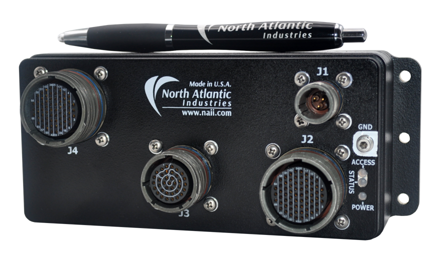
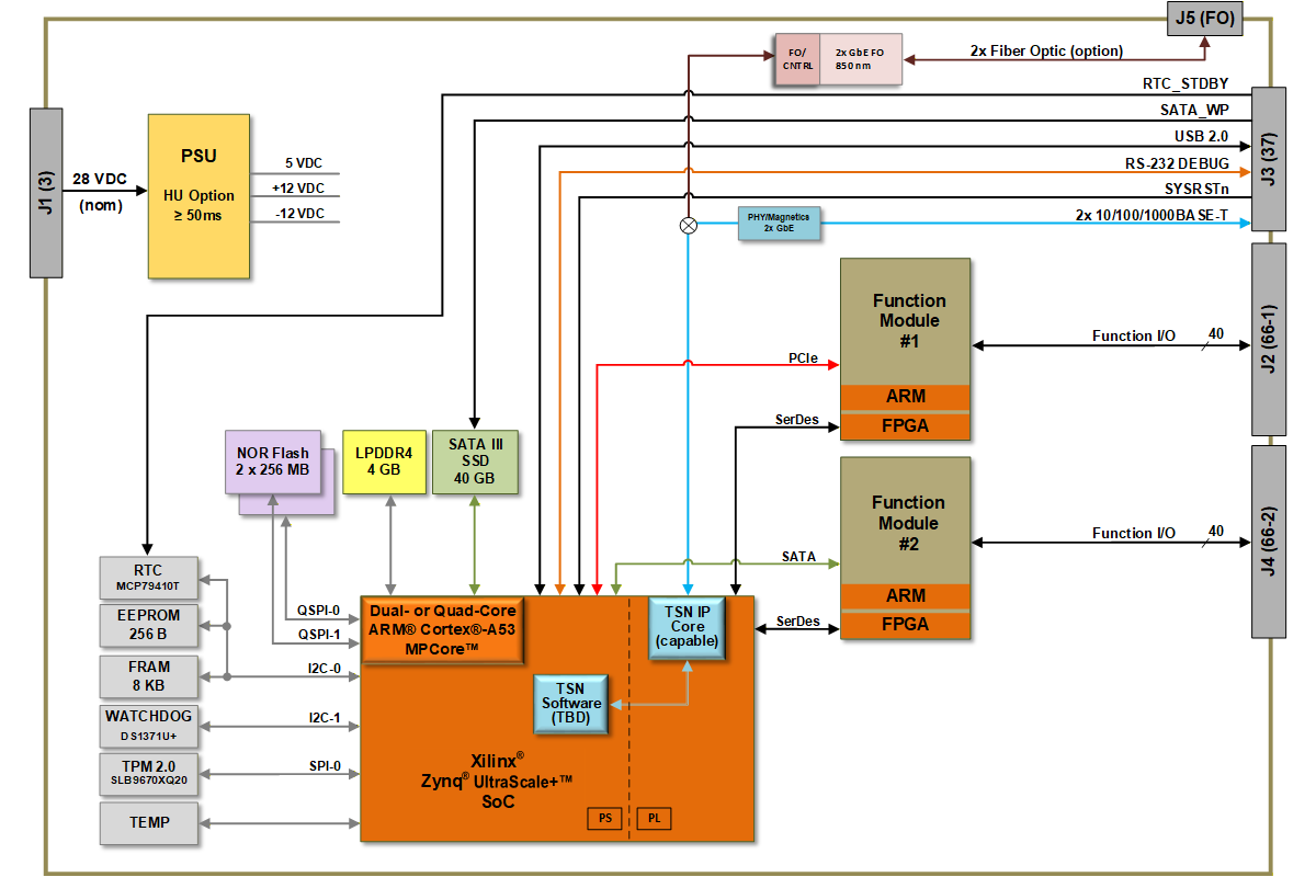
Features
|
Supports two NAI smart I/O function modules
Minimized SWaP Footprint
Ideally suited for:
|
Xilinx Zynq UltraScale+ SoC with Dual/Quad Core ARM-A53
Connectivity
Power Supply Hold-up (Optional)
Continuous Background BIT |
Operating System Support
Commercial and Rugged applications*
*Designed to meet. Characterizations pending. EMI/EMC requires shielded cables and proper grounding practices. |
Available Function Modules
Select 2 independent functions for your application
I/O Modules
| Function | Module | Description |
|---|---|---|
| Analog-to-Digital | AD1 | 12 CH. A/D, ±10 V, Dedicated, 256 kHz (max), Sigma-Delta |
| AD2 | 12 CH. A/D, ±100 V (max), Dedicated, 256 kHz (max), Sigma-Delta | |
| AD3 | 12 CH. A/D, ±25 mA, Dedicated, 256 kHz (max), Sigma-Delta | |
| AD4 | 16 CH. A/D, ± 10 V, Multiplexed, 500 KHz Agg / 8 Ch, SAR | |
| AD5 | 16 CH. A/D, ± 50 V, Multiplexed, 500 KHz Agg / 8 Ch, SAR | |
| AD6 | 16 CH. A/D, ± 100 V, Multiplexed, 500 KHz Agg / 8 Ch, SAR | |
| ADE | 16 CH. A/D, ±10 V, Individual 16-bit SAR, 200 kHz max., Simultaneous Sampling | |
| ADF | 16 CH. A/D, ±100 V, Individual 16-bit SAR, 200 kHz max., Simultaneous Sampling | |
| Digital-to-Analog | DA1 | 12 CH. D/A, ± 10 V, 25 mA Per Channel, Current or Voltage Control |
| DA2 | 16 CH. D/A, ± 10 V, 10 mA Per Channel, No Current Control | |
| DA3 | 4 CH. D/A, ±40 V, ±100 mA, Voltage or Current Output | |
| DA4 | 4 CH. D/A, ± 20 to ± 80, 10 mA, Voltage Control Only | |
| DA5 | 4 CH. D/A, High-Voltage/High-Current Half-Bridge (2 Channels Full-Bridge) External VCC Sourced Outputs | |
| Digital IO - Differential Transceiver | DF1 | 16 CH. Differential I/O, Input: -10 V to +10 V (422), -7 V to +12 V (485) Output: -.25 V to +5 V |
| DF2 | 16 CH. 16 Channel Enhanced Differential I/O | |
| Discrete IO - Multichannel, Programmable | DT1 | 24 CH. Discrete I/O, 0-60 VDC Input/Output, Max Iout 500 mA - 2 A, Source/Sink (out) |
| DT2 | 16 CH. Discrete I/O, ±80 V Input/Output, Max Iout 600 mA, Isolated/Ch Switch (out) | |
| DT3 | 4 CH. Discrete Hi & Lo Side Switch Output @ 65V/2A (max), external individual supplied VCC & VSS per channel pair | |
| DT4 | 24 CH. Enhanced DT1 | |
| DT5 | 16 CH. Enhanced DT2 | |
| Relay | RY1 | 4 CH. Relay, 220V/2A @ 60W/62.5VA (Max), Non Latching |
| RY2 | 4 CH. Relay, 220V/2A @ 60W/62.5VA (Max), Latching | |
| Digital IO - TTL/CMOS | TL1 | 24 CH. TTL I/O, Standard Functionality, Programmable |
| TL2 | 24 CH. TTL I/O, Enhanced Functionality, Programmable | |
| Variable Reluctance | VR1 | 8 CH. Variable Reluctance Signal Input and General-Purpose Pulse Counter, ±100 V, 100 kHz (max) |
Measurement & Simulation Modules
| Function | Module | Description |
|---|---|---|
| AC Reference | AC2 | 2 CH. AC Reference Source, 47 Hz - 20 KHz, ± 3% Acc, 2 – 28 Vrms, 6 VA (Max/Ch) Power |
| AC3 | 2 CH. AC Reference Source, 47 Hz - 2.5 KHz, ± 3% Acc, 28 – 115 Vrms, 6 VA (Max/Ch) Power | |
| LVDT RVDT Measurement and Simulation | LD1 | 4 CH. LVDT/RVDT to Digital, 2-28 Vrms Input, 2-115 Vrms Exc, 47 Hz -1 KHz Freq |
| LD2 | 4 CH. LVDT/RVDT to Digital, 2-28 Vrms Input, 2-115 Vrms Exc, 1 KHz - 5 KHz Freq | |
| LD3 | 4 CH. LVDT/RVDT to Digital, 2-28 Vrms Input, 2-115 Vrms Exc, 5 KHz - 10 KHz Freq | |
| LD4 | 4 CH. LVDT/RVDT to Digital, 2-28 Vrms Input, 2-115 Vrms Exc, 10 KHz - 20 KHz Freq | |
| LD5 | 4 CH. LVDT/RVDT to Digital, 28-90 Vrms Input, 2-115 Vrms Exc, 47 Hz - 1 KHz Freq | |
| Thermocouple and RTD Measurement | RT1 | 8 CH. Resistance Temperature Detectors (RTD), 2, 3, or 4 wire, 16 Bit Res, 16.7 Hz/Ch |
| TC1 | 8 CH. Thermocouple, 4.17 - 470 Hz, ±100 mV A/D | |
| Strain Gauge Measurement | SG1 | 4 CH. Strain Gauge, 4.7 Hz - 4.8 KHz, Measurement, Conventional 4-Arm Bridge |
Communication Modules
| Function | Module | Description |
|---|---|---|
| ARINC Communications | AR1 | 12 CH. ARINC 429, 100 KHz or 12.5 KHz, RX/TX, 256 Word Tx/Rx Buffer |
| AR2 | 1 CH. ARINC 568 (CH-1, RX & TX) & 1 Channel ARINC 579 (CH-2, Programmable RX or TX), 1024-Word TX & RX Buffers per Ch. | |
| CANBus Communications | CB1 | 8 CH. CANBus, CAN 2.0 A/B, 16 K RX/TX Buffer, 1 Mb/s Max Data Rate |
| CB2 | 8 CH. CANBus, J1939, 16 K RX/TX Buffer, 500 kb/s Max Data Rate | |
| CB3 | 8 CH. CANBus, CAN 2.0 A/B (CB1) or J1939 (CB2) protocol layer programmable per channel | |
| MIL-STD-1553B | FTA | 1 CH. MIL-STD-1553 (AMC), BC, RT, BM, BM/RT, 128 KB RAM, Transformer Coupled |
| FTB | 2 CH. MIL-STD-1553 (AMC), BC, RT, BM, BM/RT, 128 KB RAM Per Channel, Transformer Coupled | |
| FTC | 4 CH. MIL-STD-1553 (AMC), BC, RT, BM, BM/RT, 128 KB RAM Per Channel, Transformer Coupled | |
| FTD | 1 CH. MIL-STD-1553 (AMC), BC, RT, BM, BM/RT, 128 KB RAM, Direct Coupled | |
| FTE | 2 CH. MIL-STD-1553 (AMC), BC, RT, BM, BM/RT, 128 KB RAM Per Channel, Direct Coupled | |
| FTF | 4 CH. MIL-STD-1553 (AMC), BC, RT, BM, BM/RT, 128 KB RAM Per Channel, Direct Coupled | |
| MIL-STD-1760 | FTJ | 1 CH. MIL-STD-1760 (1553), BC, RT, BM, BM/RT, 128 KB RAM, Transformer Coupled |
| FTK | 2 CH. MIL-STD-1760 (1553), BC, RT, BM, BM/RT, 128 KB RAM Per Channel, Transformer Coupled | |
| Serial Communications | SC1 | 4 CH. Serial, RS-232/422/423 (MIL-STD-188C)/485, Non Isolated |
| SC3 | 8 CH. (max) RS-232/422/485 Serial Communications or GPIO, Programmable, Non-isolated | |
| SC5 | 4 CH. RS-232/422/485 communications, isolated per channel and from SYS GND | |
| SC6 | 4 CH. RS-232/422/485 communications, individual SYS GND provided per channel (non-isolated) |
Storage
| Function | Module | Description |
|---|---|---|
| SATA Solid State Drive (SSD) | FM2 | 1 CH. 480 GB MLC SATA Flash, extended temp -40°C to 85°C operation |
| FM7 | 1 CH. 1 TB SATA Flash, 3D NAND MLC, 0-70 °C operation | |
| FM8 | 1 CH. 1 TB SATA TLC NAND Flash, Extended Temperature Operation | |
| FM9 | 1 CH. 1.92 TB SATA TLC NAND Flash, Extended Temperature Operation |
Combination Modules
| Function | Module | Description |
|---|---|---|
| Combo | CM5 | 2 CH. Dual-redundant MIL-STD-1553 & 8 Channel ARINC 429/575, 100 KHz or 12.5 KHz, RX or TX, 256 Word Tx/Rx Buffer |
| CM8 | 2 CH. Dual-redundant MIL-STD-1553 & 12 Channel Discrete I/O, 0-60 VDC Input/Output, Max Iout 500 mA - 2 A, Source/Sink (out) | |
| CME | 8 CH. ±10V A/D (ADE-type) & 8 Channels ±10V D/A (DA2-type), Combination |
SOFTWARE SUPPORT
The ENAIBL Software Support Kit (SSK) is supplied with all system platform based board level products. This platform’s SSK contents include html format help documentation which defines board specific library functions and their respective parameter requirements. A board specific library and its source code is provided (module level ‘C’ and header files) to facilitate function implementation independent of user operating system (O/S). Portability files are provided to identify Board Support Package (BSP) dependent functions and help port code to other common system BSPs. With the use of the provided help documentation, these libraries are easily ported to any 32-bit O/S such as RTOS or Linux.
The latest version of a board specific SSK can be downloaded from our website www.naii.com in the software downloads section. Software setup is covered in Choosing the Right SSK and the SSK package guides (SSK 1.x, SSK 2.x); packages are on the Downloads page. For other operating system support, contact factory.
CONVENTIONS USED IN THIS MANUAL

Note
An operating procedure, practice, or condition, etc., that is essential to emphasize.
All numbers are expressed in decimal format unless otherwise noted.
Website
GENERAL SAFETY NOTICES
The following general safety notices supplement the specific warnings and cautions appearing elsewhere in the manual. They are recommended precautions that must be understood and applied during operation and maintenance of the instrument covered herein.
Death or serious injury may result if personnel fail to observe safety precautions. Dependent on configuration, some modules (e.g. Synchro / Resolver or AC signal sources) can generate output signals with high voltages. Be careful not to contact high-voltage connections when installing, operating or maintaining this instrument.

The NIU2U is delivered as a standalone system with no accessible or serviceable parts.
Repair
DO NOT ATTEMPT REPAIR. Under no circumstances should repair of this instrument be attempted. All repairs to this chassis must be accomplished at the factory.
High Voltage

HIGH VOLTAGE may be used in the operation of this equipment.
Input Power Always On

Note
The design of the model NIU2U is such that DC input power is continuously supplied to internal circuits when connected to a main power source. To disconnect the NIU2U from external power, the external power source should first be de-energized. The power input cable can then be disconnected.
SYSTEM SPECIFICATIONS & DETAILS
Introduction
The Nano Interface Unit (NIU2U) is a second-generation, integrated, compact, “nano-sized” subsystem with unprecedented I/O capability configurations. The NIU2U connects to existing platform Ethernet networks, making data available to any system on the network. Optionally, the NIU2U can be delivered with Dual or Quad ARM® Cortex®-A53 access support for standalone or other processor related capability.
The NIU2U easily adds sensor data acquisition and distribution and communication interfaces to mission computers without expensive chassis and backplane redesign. It has been designed with rugged embedded industrial, military and aerospace applications in mind. Leveraging NAI’s field-proven, unique modular architecture, the NIU2U supports a wide selection of different Intelligent I/O, motion simulation/measurement and communications functions such as:
| A/D Converter | D/A Converter | I/O TTL/CMOS | RTD | I/O Discrete |
| I/O Differential Transceiver | Synchro/Resolver LVDT/RVDT Measurement | Synchro/Resolver LVDT/RVDT Simulation | Strain Gage | Encoder |
| Dual-Channel Dual Redundant BC/RT/MT MIL-STD-1553 | High-Speed Sync/Async RS232/422/423/485 | ARINC 429/575 | CANBus | I/O Relay |
| AC Reference | Ethernet Switch | SSD/Flash |
This approach provides unprecedented flexibility for supporting existing or new applications where there are specific interfacing requirements. Significant application benefits include:
- Independent (pre-processed) I/O functionality targeted to specific data acquisition/control areas
- Additional capabilities, technology insertion and sensor interfacing to existing fielded applications
- Minimal integration risk based on current field-proven, deployed technologies
- Only ~ 3.1”H x 2.7”D x 7.3”W @ ~2.17 lbs. (984 g) conduction/convection cooled
- 2x 10/100/1000Base-T Ethernet ports, 1x RS-232 debug port, and 1x USB 2.0 ports
Objectives
This manual provides the user with basic hardware implementation and information regarding the operation and interface of the NIU2U. Each NIU2U is fitted with one or two function modules and an integrated motherboard, power supply unit (PSU) and interface connectors.
Scope
This manual covers the basic operation of the NIU2U as a standalone I/O subsystem with pertinent/specific details relating to the operation/communications from/to the NIU2U with the available function module(s) fitted within the NIU2U.
ON BOARD RESOURCES
Memory
DDR4 SDRAM
The NIU2U provides a total of 4 GB of LPDDR4 memory. This memory is organized as one 1 Gig x 32 MT53E1G32D2FW device (parts may vary). The Ultrascale+™ has an on chip 64-bit DDR4 memory controller. Please consult the Micron data sheet for LP DDR4 device specific details.
NOR Flash
Connected through the local bus, the NIU2U supports 2 x 2 gigabytes of flash. The Flash consists of a stacked (four 512Mb die) Micron® Flash MT25QL02GCBB8E12-0SIT device. Flash features a high-speed SPI-compatible bus interface that utilizes dual QSPI via a two-input logic gate to increase I/O throughput rates four times for each device. The NOR Flash has an erase capacity of 100,000 cycles per sector and typical data retention of 20 years.
FRAM
The FM24CL64B is a 64-kilobit nonvolatile memory employing an advanced ferroelectric process. The ferroelectric random-access memory or FRAM is nonvolatile and performs reads and writes like a RAM. It provides reliable data retention for 38 years. The NIU2U FRAM 64K bits are organized as 8,192 x 8 bits random access memory, connected to the Ultrascale+™ CPU through the I2C controller.
SATA
The Ultrascale+™ CPU is directly connected to an onboard Solid-State Drive (SSD). The SSD contains a single level cell NAND Flash together with a controller in a single Multi-Chip package. The Multi-Chip packaged device is soldered directly to the printed circuit board for reliable electrical and mechanical connection.
The SSD has an internal write protect signal SATA_WP. The SATA_WP signal must be connected or switched to ground to enable any write to the SSD. The SATA_WP signal is pulled up on card by a 4.7 KΩ resistor to the internal 3.3 V supply.
The onboard SATA drive conforms to the follow specifications:
- Complies with Serial ATA 2.5 Specification
- Supports speeds: 1.5 Gbps (first-generation SATA), 3 Gbps (second-generation SATA and eSATA)
- Supports advanced technology attachment packet interface (ATAPI) devices
- Contains high-speed descriptor-based DMA controller
- Supports native command queuing (NCQ) commands
The standard ordering code for the NIU2U includes a 32GB SSD drive. Larger devices are available; please consult the factory for availability.
Peripheral I/O
Ethernet
The NIU2U supports two 10/100/1000Base-TX Ethernet connections using two Marvell Alaska 88E1512 Ethernet PHY devices and the Xilinx Gigabit Ethernet MACs. The PHY-to-MAC interface employs a Reduced Gigabit Media Independent Interface (RGIII) connection using four data lines at 250 Mbps each for a connection speed of 1 Gbps. The NIU2U contains internal magnetics and can directly drive copper CAT5e or CAT6 twisted pairs.
The NIU2U Ethernet ports support:
- Detection and correction of pair swaps (MDI crossover), and pair polarity
- MAC-side and line-side loopback
- Auto-negotiation
Ethernet Port 1 can be routed as 10/100/1000Base-TX Ethernet as a build option.
Ethernet Port 2 can be routed as 10/100/1000Base-TX Ethernet as a build option.
I/O pin outs can be found in the Pinout Details section of this document.
USB
The NIU2U supports one USB 2.0 port. Contact factory for availability.
USB is available on the NIU2U, on connector J2. The USB port can operate as a standalone host.
- Compatible with USB specification, Rev. 2.0
- Supports high-speed (480 Mbps), full-speed (12 Mbps), and low-speed (1.5 Mbps) operations
- Supports operation as a standalone USB host controller
- Supports USB root hub with one downstream-facing port
- Enhanced host controller interface (EHCI)-compatible
- One controller supports operation as a standalone USB device
- Supports one upstream-facing port
- Supports six programmable USB endpoints
I2C
I2C is a two-wire, bidirectional single ended serial bus that provides an efficient method of exchanging data between a master and slave device. The NIU2U has one I2C device for communicating with onboard devices, as shown in the table below.
| Assignment | I2C addresses | Device |
|---|---|---|
| Onboard Devices | 0x68 | Counter |
| Onboard Devices | 0x56 | EEPROM |
| Onboard Devices | 0x53 | FRAM |
Serial Port
The NIU2U has a single, asynchronous serial port. The interface uses a two-wire, TXD, RXD interface (system/power GND referenced). The SER-TXD and SER-RXD RS-232 signals are routed to J3 on the NIU2U.
Software Libraries/Associated Documents
NIU2U BSP Processor Module Library
The NIU2U Processor library package provides function interfaces to the on-module functionality. This package contains Help documentation (in html format) that explains all the functions available in the library. The package also contains the source code (**.h, **.c) files as well as the files needed to build the library using any of the supported operating systems. Example programs are also provided to demonstrate the usage of the libraries in typical applications of the module.
Associated Documents
Check the NAI website or contact factory for the latest downloads and documentation.
SPECIFICATIONS
The NIU2U is designed to meet the following general specifications.
General
| Ethernet Data Transfer: | Data transfers within 1 ms (typical) |
| Input Voltage: | 18 to 36 VDC (28 VDC nominal) |
| Power (Base unit): | ~8 W @ 28 V VDC nominal plus module(s) power (see specific module(s) specifications) I/O Signal GND reference is isolated from main power source return and chassis. |
| Power/Heat Dissipation: | 15 watts (maximum) when properly mounted to a cold-plate, which must be maintained at a temperature not to exceed 71°C. Note: The total NIU2U power dissipation is dependent on the configuration of the modules fitted in the NIU2U. |
| Temperature, Operating: | -40°C to 71°C (conduction cooled - measured at cold plate interface) |
| Temperature, Storage: | -55°C to 105°C |
| Size: | Height: 3.1” (79 mm) Depth: 2.7” (69 mm) Width: 7.3” (185 mm) |
| Weight: | The weight of an NIU2U system is dependent on the configuration. The approximate weight of the NIU2U is based on the selection of the functional module. The approximate weight of a typical fully configured NIU2U (model #) is ~2.17 lbs. (984 g). |
Environmental
| Environmental MIL-STD-810 (*1) | ||||||
| No. | Description | Procedure | Cycles | Table | Figure | Comments |
| 514 | Random Vibe | Method 514.6, 0.1g /Hz from 100 to 1K Hz., -3dB octave 5-100 Hz and -6dB 1K-2K Hz,(operational) | ||||
| 514 | Sinusoidal Vibe | TBD | ||||
| 501 | Temp (High) | 3 | 3 periods (@ 4 hrs. ea.) within 24 hrs. cycle at 71 C baseplate | |||
| 502 | Temp (Low) | 1 | 3 periods (@ 4 hrs. ea.) within 24 hrs. cycle at -40 C baseplate | |||
| 503 | Temp (Shock) | 3 | 3 x 1 hr. each hot & cold cycle | |||
| 507 | Humidity | II | 10 | 507.5-7 | 507.5-IX | Cyclic high humidity (Cycle B2) |
| 500 | Altitude (50K) | II | 1 | n/a | n/a | 10m/s to 50,000ft for 1 hr. |
| 513 | Acceleration | II | 1 | 513.6-II | n/a | Carrier-based Aircraft (18g's max) |
| 516 | Shock - Operating | I | 3 | 516.6-I | n/a | 40g's, 1 min each x 6 axis (total of 18 shock pulses) |
| 516 | Shock - Crash | V | 3 | 516.6-I | n/a | 75g's, 1 min each x 6 axis (total of 18 shock pulses) |
| Ingress Protection IEC 60529 (*1) | ||||||
| No. | Description | Procedure | Cycles | Table | Figure | Comments |
| IP54 | Dust Protection | |||||
| IP54 | Water Splashing | |||||
| IP65 | Dust Tight | |||||
| IP65 | Water Jets | |||||
EMC/EMI
| EMC / MIL-STD-461 (*1, *2) | ||
| MIL-STD-461(G) | Method/Curve/Procedure | Comments |
| CE102 | Conducted emissions, power leads, 30 Hz to 10 kHz. | |
| CS101 | Conducted emissions, power leads, 10 kHz to 10 MHz | |
| CS106 | Conducted susceptibility, power leads, 30 Hz to 150 kHz. | |
| CS114 | Conducted susceptibility, transients, power leads | |
| CS115 | Conducted susceptibility, bulk cable injection, 10 kHz to 200 MHz | |
| CS116 | Conducted susceptibility, bulk cable injection, impulse excitation | |
| RE101 | Conducted susceptibility, damped sinusoidal transients, cables and power leads, 10 kHz to 100 MHz | |
| RE102 | Radiated emissions, magnetic field, 30 Hz to 100 kHz. | |
| RS101 | Radiated emissions, electric field, 10 kHz to 18 GHz. | |
| RS103 | Radiated, susceptibility, magnetic field, 30 Hz - 100 kHz | |
Notes:
*1 - Designed to meet / Generic Test Reports (contact factory for availability).
*2 - Utilizing proper shielded cables and system practices.
Note
Specifications are subject to change without notice.
MTBF
The Mean Time between Failures is configuration, environment, and temperature dependent. Please contact factory regarding calculations based on the specific configuration and program requirements.
UNPACKING & INSPECTION
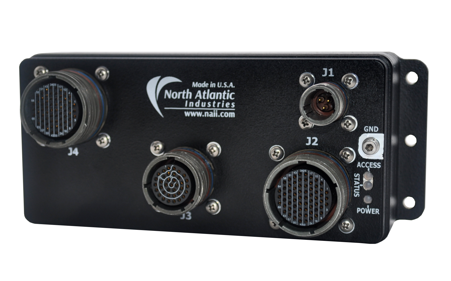
Figure 1. NIU2U
Unpacking
The NIU2U packing materials were designed specifically for transport protection of the NIU2U. When receiving the shipment container, inspect packaging for any evidence of physical damage. If damage is evident, it is recommended that the carrier agent is present when opening the shipping container. It is further recommended that all packing material is retained in the event the NIU2U needs to be shipped elsewhere.
System/Chassis Identification
An identification label, indicating part number, unique serial number, and Ethernet PHY MACs / default IP address(es) is affixed to the top of the system chassis.
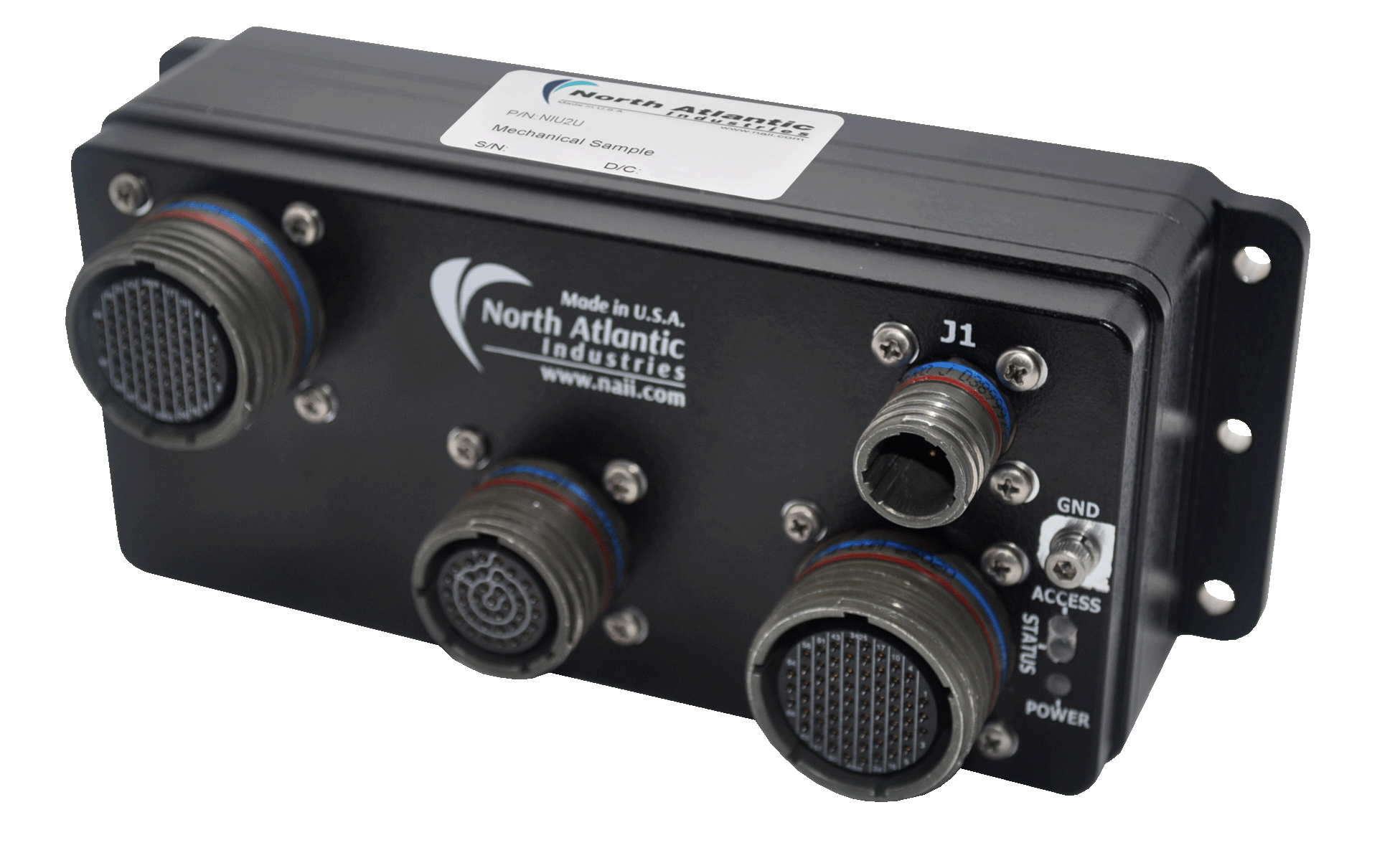
Figure 2. Unit Identification
Inspection
Inspect the chassis and connectors to ensure that they were not damaged during transit.
MECHANICAL INTERFACE
Mechanical Description
The NIU2U is a rugged, aluminum, conduction-cooled system. It must be mounted to a cold plate. The system thermal management design considerations should ensure that the chassis thermal interface (NIU2U bottom surface) does not exceed 71°C. Mounting holes are provided on the chassis bottom housing flanges (as depicted). See the outline drawing below.
Mounting Requirements
Refer to NIU2U Outline and Installation Drawing (OID) for details on mounting and installing the NIU2U. It is available for download from NAI’s website. The NIU2U is conduction cooled and must be mounted in accordance with the drawing. The OID provides recommended hardware, torque, cold-plate flatness and surface finish specifications, and thermal conductivity requirements.
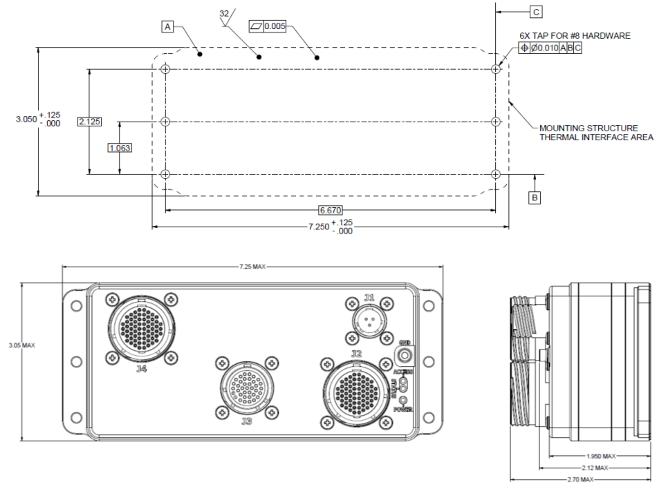
Figure 3. NIU2U Outline Dimensions/Cold Plate Mounting Pattern (Reference Only)
Note
- For reference only (refer to the product web page for the latest revision NIU2U Outline and Installation Drawing (OID).
- Unless otherwise specified, dimensions are in inches (mm); tolerances are:
2 PL DEC ±0.01; 3 PL DEC ±0.005
FRACT ±1/64 (0.4); ANGLES ±1/2 (12.7)
Chassis (Earth) GND
Chassis ground point threaded insert location is on the connector side of the NIU2U as shown.
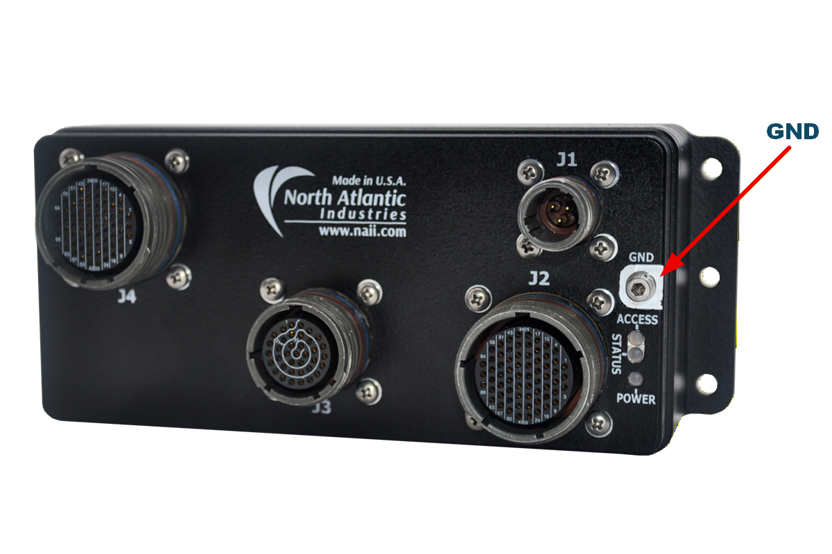
Figure 4. NIU2U Outline Dimensions/Chassis GND location
Note
Chassis GND braid or equivalent to be secured by #6-32 screw/studs (with a depth of 0.3 inches) as end application requires. The NIU2U chassis is provided with #6-32 threaded insert only. The recommended torque for the NIU2U Chassis GND screw is 6 in-lbs. (68 N·cm) min. / 8 in-lbs. (90 N·cm) max.
CONNECTOR DESIGNATION & DESCRIPTION
The Power, I/O Interface and Ethernet connectors are located on the NIU2U front panel housing.
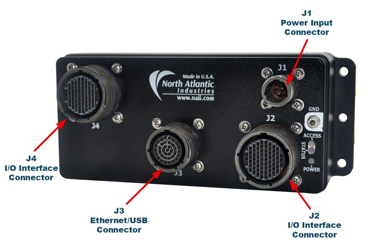
Figure 5. NIU2U (Front Panel Connector Placement)
NIU2U Connector Designation and Description
| Connector Designation | Description |
| J1 | Primary Power Connector, VDC |
| J2 | I/O Connector 1, Smart Module I/O Slot-1 |
| J3 | 2x GbE, Maintenance, Debug (RS-232, System Reset) & extended processor option signals (RS-232, Hardware SATA Write Protect) |
| J4 | I/O Connector 2, Smart Module I/O Slot-2 |
Connector Details and Pinout
Generic pinout. See module I/O section or contact factory regarding any special module I/O configuration.
J1, Primary Power Connector
Primary input power is supported on the NIU2U via the J1 connector. Connectors used are as follows:
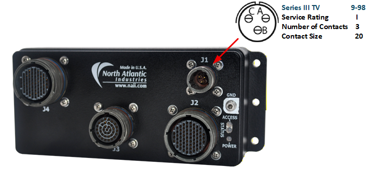
Figure 6. J1 Primary Power Connector Detail
Parts Identification
J1 Primary Power Connector Definition
| Chassis (Box-level) | Mating Cable Connector | ||||
| Designation | MIL-DTL Equivalent Reference | Shell/Insert | Pin-count | MIL-DTL Equivalent Reference | NAI P/N (for reference) |
| J1 | D38999/20WA98PA (10,000 pF, incl. 'c-filter') | 9 / 98 | 3 | D38999/26WA98SA | 05-0297-COM |
Pinout
J1 Primary Power Connector Pinout
| J1 Connector Pin | Signal |
| A | Chassis GND |
| B | 28VDC-RTN |
| C | 28VDC |
J2, I/O, Module 1
The NIU2U supports up to two Smart function modules. The J2 I/O connector supports Module-1 function I/O.
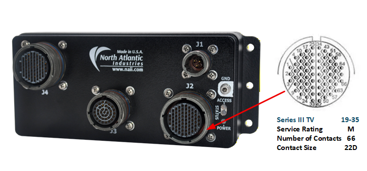
Figure 7. J2 I/O Module-1
Parts Identification
J2 Ethernet Connector Definition
| Chassis (Box-level) | Mating Cable Connector | ||||
| Designation | MIL-DTL Equivalent Reference | Shell/Insert | Pin-count | MIL-DTL Equivalent Reference | NAI P/N (for reference) |
| J2 | D38999/20WF35SN | 19 / 35 | 66 | D38999/26WF35PN | 05-0284 |
Pinout
Generic pinout. See module I/O section or contact factory regarding any special module I/O configuration.
| J2 Connector Pin | Signal | Notes |
| 1 | MOD1-DATIO24 | |
| 2 | MOD1-DATIO14 | |
| 3 | MOD1-DATIO13 | |
| 4 | MOD1-DATIO31 | |
| 5 | MOD1-DATIO23 | |
| 6 | MOD1-DATIO12 | |
| 7 | MOD1-DATIO11 | |
| 8 | MOD1-DATIO08 | |
| 9 | MOD1-DATIO07 | |
| 10 | MOD1-DATIO32 | |
| 11 | MOD1-DATIO22 | |
| 12 | MOD1-DATIO21 | |
| 13 | MOD1-DATIO10 | |
| 14 | MOD1-DATIO09 | |
| 15 | MOD1-DATIO06 | |
| 16 | MOD1-DATIO05 | |
| 17 | MOD1-DATIO34 | |
| 18 | MOD1-DATIO33 | |
| 19 | MOD1-DATIO20 | |
| 20 | MOD1-DATIO19 | |
| 21 | MOD1-DATIO04 | |
| 22 | MOD1-DATIO03 | |
| 23 | MOD1-DATIO02 | |
| 24 | MOD1-DATIO01 | |
| 25 | MOD1-DATIO36 | |
| 26 | MOD1-DATIO35 | |
| 27 | MOD1-DATIO18 | |
| 28 | MOD1-DATIO17 | |
| 29 | MOD1-DATIO16 | |
| 30 | MOD1-ETH3-TP3N | *1 |
| 31 | MOD1-ETH3-TP3P | *1 |
| 32 | MOD1-ETH3-TP1N | *1 |
| 33 | MOD1-ETH3-TP1P | *1 |
| 34 | MOD1-DATIO38 | |
| 35 | MOD1-DATIO37 | |
| 36 | MOD1-DATIO26 | |
| 37 | MOD1-DATIO25 | |
| 38 | MOD1-DATIO15 | |
| 39 | MOD1-ETH3-TP2N | *1 |
| 40 | MOD1-ETH3-TP2P | *1 |
| 41 | MOD1-ETH3-TP0N | *1 |
| 42 | MOD1-ETH3-TP0P | *1 |
| 43 | MOD1-DATIO40 | |
| 44 | MOD1-DATIO39 | |
| 45 | MOD1-DATIO28 | |
| 46 | MOD1-DATIO27 | |
| 47 | MOD1-ETH2_4-TP3_2N | *1 |
| 48 | MOD1-ETH2_4-TP3_2P | *1 |
| 49 | MOD1-ETH2_4-TP1_0N | *1 |
| 50 | MOD1-ETH2_4-TP1_0P | *1 |
| 51 | GND | Signal/System Ground |
| 52 | MOD1-DATIO30 | |
| 53 | MOD1-DATIO29 | |
| 54 | MOD1-ETH2-TP2N | *1 |
| 55 | MOD1-ETH2-TP2P | *1 |
| 56 | MOD1-ETH2-TP0N | *1 |
| 57 | MOD1-ETH2-TP0P | *1 |
| 58 | GND | Signal/System Ground |
| 59 | MOD1-ETH1-TP2N | *1 |
| 60 | MOD1-ETH1-TP3N | *1 |
| 61 | MOD1-ETH1-TP3P | *1 |
| 62 | MOD1-ETH1-TP1N | *1 |
| 63 | MOD1-ETH1-TP1P | *1 |
| 64 | MOD1-ETH1-TP2P | *1 |
| 65 | MOD1-ETH1-TP0N | *1 |
| 66 | MOD1-ETH1-TP0P | *1 |
Note
*1: Defines and utilized only for special “high-speed” module I/O pinout (supports modules e.g. TE1, TE2, FW1, EM1, etc.)
J3, Ethernet Communications & Debug
The NIU2U supports up to two 10/100/1000Base-T ports (when appropriately configured) and debug/maintenance signals. The debug/maintenance signals provided are an RS-232 console port and System Reset (for a soft reset/reload). Additionally, typically for ARM/processor optioned configurations, a USB 2.0 port, Hardware Write Protect (for SATA accessibility) and a Real Time Clock Standby (i.e. auxiliary 3.3V/battery backup for the real time clock) are also provided.
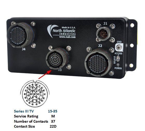
Figure 8. J3 Ethernet Communications & Debug Connector Detail
Parts Identification
J3 Ethernet Communications & Debug Connector Definition
| Chassis (Box-level) | Mating Cable Connector | ||||
| Designation | MIL-DTL Equivalent Reference | Shell/Insert | Pin-count | MIL-DTL Equivalent Reference | NAI P/N (for reference) |
| J3 | D38999/20WD35SN | 15 / 35 | 37 | D38999/26WD35PN | 05-0302 |
Pinouts
J3 Ethernet Communications & Debug Connector Pinout
| J3 Connector Pin | Signal | Notes |
| 1 | ETH2-TP2+ | *7 |
| 2 | ETH2-TP0+ | *7 |
| 3 | ETH2-TP1+ | *7 |
| 4 | ETH2-TP1- | *7 |
| 5 | ETH1-TP0+ | *7 |
| 6 | ETH1-TP0- | *7 |
| 7 | ETH1-TP3+ | *7 |
| 8 | ETH1-TP3- | *7 |
| 9 | ETH1-TP1+ | *7 |
| 10 | ETH1-TP1- | *7 |
| 11 | (+)5V-USB | *4 |
| 12 | USB-GND | *4, 6 |
| 13 | USB-DM | *4 |
| 14 | USB-DP | *4 |
| 15 | RTC_STDBY | *5 |
| 16 | SER-GND | *2, 6 |
| 17 | SER-RXD1 | *2 |
| 18 | SER-TXD1 | *2 |
| 19 | ETH2-TP2- | *7 |
| 20 | ETH2-TP0- | *7 |
| 21 | ETH2-TP3+ | *7 |
| 22 | ETH2-TP3- | *7 |
| 23 | ETH1-TP2+ | *7 |
| 24 | ETH1-TP2- | *7 |
| 25 | GND | *6 |
| 26 | (J3-26) | *8 |
| 27 | (J3-27) | *8 |
| 28 | SYSRSTn | *1 |
| 29 | HDW_WP | *3 |
| 30 | GND | *6 |
| 31 | GND | *6 |
| 32 | GND | *6 |
| 33 | GND | *6 |
| 34 | (J3-34) | *8 |
| 35 | (J3-35) | *8 |
| 36 | (J3-36) | *8 |
| 37 | GND | *6 |
Notes
-
SYSRSTn: An active “low” or GND logic level (as referenced to System GND of the NIU2U) assertion of the SYSRST# signal (internally pulled ‘high’) on the NIU2U processor and module cards will initiate an NIU2U system reset.
-
Debug: RS-232 Serial Communications Console port
-
Hardware-Write Protect: Used for SATA Flash write enable/disable on the processor accessible version of the NIU2U. OPEN for Write Protect, GND for Write Enable. (ARM option only)
-
USB: USB 2.0 compatibility - accessible with processor accessible version of the NIU2U.(ARM option only).
-
RTC_STDBY: +3.3V (nom) battery backup for Real Time Clock (RTC) circuit. GND (System GND referenced). (ARM option only)
-
GND, SER-GND, USB-GND: All the identified GNDs are referenced to the same internal signal GND (System GND).
-
ETHx-TPyz: Standard NIU2U configuration provides 2x 10/100/1000Base-T Ethernet ports. If the Gigabit Fiber Optic (Gb FO) connection is specified, the Ethernet functionality will not be available These signals are considered no-connects (N/C).
-
(J3-xx): Signals are undefined in the standard NIU2U configurations. These signals are considered no-connects (N/C).
J4, I/O, Module 2
The NIU2U supports up to two Smart function modules. The J4 I/O connector supports Module-2 function I/O.
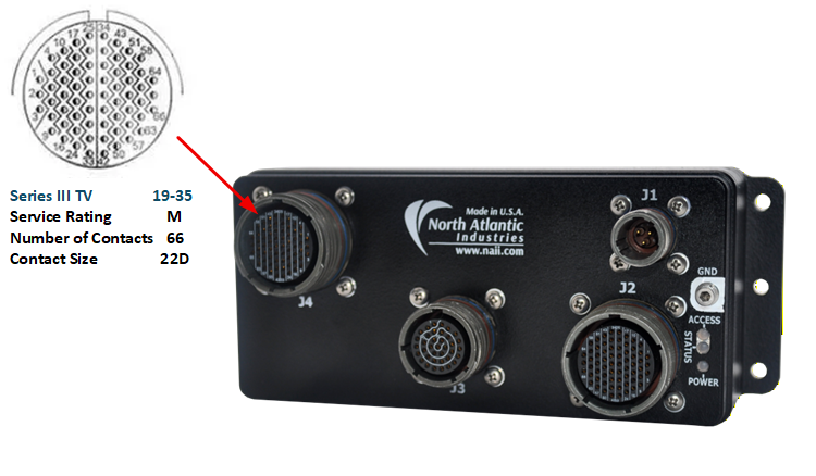
Figure 9. J4 I/O Module-2 Connector Detail
Parts Identification
J4 I/O Module-2 Connector Definition
| Chassis (Box-level) | Mating Cable Connector | ||||
| Designation | MIL-DTL Equivalent Reference | Shell/Insert | Pin-count | MIL-DTL Equivalent Reference | NAI P/N (for reference) |
| J4 | D38999/20WF35SA | 19 / 35 | 66 | D38999/26WF35PA | 05-0285 |
Pinout
Generic pinout. See module I/O section or contact factory regarding any special module I/O configuration.
J4 I/O Module-2 Connector Pinout
| J4 Connector Pin | Signal | Notes |
| 1 | MOD2-ETH1-TP0N | *1 |
| 2 | MOD2-ETH1-TP0P | *1 |
| 3 | MOD2-ETH1-TP2N | *1 |
| 4 | MOD2-ETH1-TP1P | *1 |
| 5 | MOD2-ETH1-TP1N | *1 |
| 6 | MOD2-ETH1-TP3P | *1 |
| 7 | MOD2-ETH1-TP3N | *1 |
| 8 | MOD2-ETH1-TP2P | *1 |
| 9 | GND | Signal/System Ground |
| 10 | MOD2-ETH2-TP0P | *1 |
| 11 | MOD2-ETH2-TP0N | *1 |
| 12 | MOD2-ETH2-TP2P | *1 |
| 13 | MOD2-ETH2-TP2N | *1 |
| 14 | MOD2-DATIO27 | |
| 15 | MOD2-DATIO28 | |
| 16 | GND | Signal/System Ground |
| 17 | MOD2-ETH2_4-TP1_0P | *1 |
| 18 | MOD2-ETH2_4-TP1_0N | *1 |
| 19 | MOD2-ETH2_4-TP3_2P | *1 |
| 20 | MOD2-ETH2_4-TP3_2N | *1 |
| 21 | MOD2-DATIO26 | |
| 22 | MOD2-DATIO25 | |
| 23 | MOD2-DATIO40 | |
| 24 | MOD2-DATIO39 | |
| 25 | MOD2-ETH3-TP0P | *1 |
| 26 | MOD2-ETH3-TP0N | *1 |
| 27 | MOD2-ETH3-TP2P | *1 |
| 28 | MOD2-ETH3-TP2N | *1 |
| 29 | MOD2-DATIO11 | |
| 30 | MOD2-DATIO22 | |
| 31 | MOD2-DATIO21 | |
| 32 | MOD2-DATIO38 | |
| 33 | MOD2-DATIO37 | |
| 34 | MOD2-ETH3-TP1P | *1 |
| 35 | MOD2-ETH3-TP1N | *1 |
| 36 | MOD2-ETH3-TP3P | *1 |
| 37 | MOD2-ETH3-TP3N | *1 |
| 38 | MOD2-DATIO09 | |
| 39 | MOD2-DATIO20 | |
| 40 | MOD2-DATIO19 | |
| 41 | MOD2-DATIO36 | |
| 42 | MOD2-DATIO35 | |
| 43 | MOD2-DATIO12 | |
| 44 | MOD2-DATIO10 | |
| 45 | MOD2-DATIO08 | |
| 46 | MOD2-DATIO07 | |
| 47 | MOD2-DATIO17 | |
| 48 | MOD2-DATIO18 | |
| 49 | MOD2-DATIO34 | |
| 50 | MOD2-DATIO33 | |
| 51 | MOD2-DATIO01 | |
| 52 | MOD2-DATIO04 | |
| 53 | MOD2-DATIO03 | |
| 54 | MOD2-DATIO16 | |
| 55 | MOD2-DATIO15 | |
| 56 | MOD2-DATIO32 | |
| 57 | MOD2-DATIO31 | |
| 58 | MOD2-DATIO02 | |
| 59 | MOD2-DATIO05 | |
| 60 | MOD2-DATIO14 | |
| 61 | MOD2-DATIO13 | |
| 62 | MOD2-DATIO30 | |
| 63 | MOD2-DATIO29 | |
| 64 | MOD2-DATIO06 | |
| 65 | MOD2-DATIO24 | |
| 66 | MOD2-DATIO23 |
Notes
*1: Defines special “high-speed” module I/O pinout (includes special modules e.g. TE1, TE2, FW1, EM1, etc.)
POWER-UP & OPERATIONAL DESCRIPTION
Panel LEDs & Functions
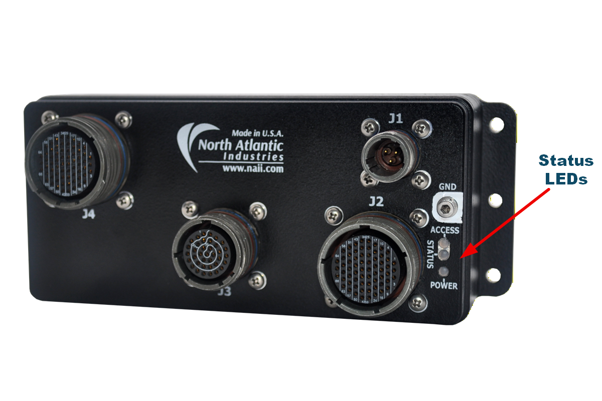
Figure 10. NIU2U Status LEDs Location
NIU2U Status LEDs Function
| LED | STATUS / FUNCTION | |
| ILLUMINATED | EXTINGUISHED | |
| POWER (GRN:) | Blinking: Initializing Steady On: Power-On/Ready | Power-off |
| ACCESS (YEL): | Blinking: Unit Access (GbE activity) | No Unit Access or Activity |
| STATUS (RED): | Module BIT (Attention required) | No Module BIT Attention Required |
Basic Operations
Primary SBC/host/mission computer communications interface to the NIU2U is via the Gig-E port(s). Full command/control/register data query is requested and sent as a TCP/IP or UDP type message to the NIU2U via NAI Ethernet protocol structure, i.e. the NIU2U receives a message command and replies accordingly. In addition to direct read/write function module register access, once initialized the protocol can also support multi-register block read/writes as well as generate interrupt driven output messages or timed interval data ‘dump’ messages. For detailed supplement, please visit the NIU2U model page and refer to:
NAI Ethernet Interface for Generation 5 SBC and Embedded IO Boards Software Specification
The NIU2U is delivered as a tested unit. All operations have been verified. It is recommended that Power and Ethernet connections be made to verify operation of the function module(s) fitted within the NIU2U by making use of NAI’s “Embedded Soft Panel” (ESP), which can be utilized as a board/module level debugging tool (if the NIU2U function module configuration supports).
For more information on using the ESP and accessing the appropriate development resources and documentation for the product, please refer to NAI’s Product Documentation site.
REGISTER MEMORY MAP ADDRESSING
The register map address consists of the following:
- cPCI/PCIe BAR or Base Address for the Board
- Module Slot Base Address
- Function Offset Address
Board Base Address
The table below lists the BAR used for access to the motherboard and module registers. The second BAR is used internally for motherboard and module firmware updates. The other cPCI/PCIe BARs not listed are not used.
| NAI Boards | Device ID | Bus | Motherboard and Module Register Access | Motherboard and Module Firmware Updates |
| Slave Boards | ||||
| NIU2U | N/A | N/A | Direct Memory Access | Internal Direct Memory Access |
Module Slot and Function Address
The memory map for the modules are dependent on the types of modules on the board and the order in which the modules are installed on the board as well as the firmware installed on the motherboard. The function modules are enumerated allowing for dynamic memory space allocation and therefore the “start” address of the module function register area is factory pre-defined (and read from) the Module Address register.
Register Memory Map Addressing Example for NIU2U
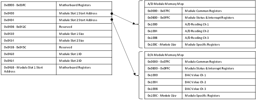
Figure 12. Register Memory Map Addressing Example for NIU2U
Address Calculation
Motherboard Registers:
Read/Write access to the motherboard registers starts with the base address for the board and then the motherboard base offset address.
For example, to address Module Slot 1 Start Address register (i.e. register address = 0x0400):
- Start with the base address for the board.
- Add the motherboard base register address offset.
| Motherboard Address = | Base Address + | Motherboard Address Offset | = 0x9000 0400 |
| 0x9000 0000 | 0x0400 |
Module Registers:
Read/Write access to the Function module’s registers start with the base address of the board. Add the “content” for the Module Start Address and then, add the specific module function register offset.
For example, to address an appropriate/specific function module with a register offset:
- Start with the base address for the board.
- Add the value (contents) from the module base address offset register (contents/value of Motherboard Memory register for Module 1 (i.e., @ 0x0400) = 0x4000.
- Then add the specific module function Register Offset of interest (i.e., 0x1000)
| (Function Specific) Address = | Base Address + | Module Base Address Offset + | Function Register Offset | = 0x9000 5000 |
| 0x9000 0000 | 0x4000 | 0x1000 |
REGISTER DESCRIPTIONS
Module Information Registers
The Module Slot Address, Module Slot Size and Module Slot ID provide information about the modules detected on the board.
| Module Slot Addressing Ready | |
| Function: | Indicates that the module slots are ready to be addressed. |
| Type: | unsigned binary word (32-bit) |
| Data Range: | 0x0000 0000 to 0xFFFF FFFF |
| Read/Write: | R |
| Initialized Value: | 0xA5A5A5A5 |
| Operational Settings: | This register will contain the value of 0xA5A5A5A5 when the module addresses have been determined. |
| Module Slot Address | |
| Function: | Specifies the Base Address for the module in the specific slot position. |
| Type: | unsigned binary word (32-bit) |
| Data Range: | 0x0000 0000 to 0xFFFF FFFF |
| Read/Write: | R |
| Initialized Value: | Based on board's module configuration. |
| Operational Settings: | 0x0000 0000 indicates no Module found. |
| Module Slot Size | |
| Function: | Specifies the Memory Size (in bytes) allocated for the module in the specific slot position. |
| Type: | unsigned binary word (32-bit) |
| Range: | 0x0000 0000 to 0xFFFF FFFF |
| Read/Write: | R |
| Initialized Value: | Assigned by factory for the module. |
| Operational Settings: | 0x0000 0000 indicates no Module found. |
| Module Slot ID | |
| Function: | Specifies the Model ID for the module in the specified slot position. |
| Type: | 4-character ASCII string |
| Data Range: | 0x0000 0000 to 0xFFFF FFFF |
| Read/Write: | R |
| Initialized Value: | Assigned by factory for the module. |
| Operational Settings: | The Module ID is formatted as four ASCII bytes: three characters followed by a space. Module IDs are in little-endian order with a single space following the first three characters. For example, 'TL1' is '1LT', 'SC1' is '1CS' and so forth. Example below is for “TL1” (MSB justified). All value of 0000 0000 indicates no Module found. |
| D31 | D30 | D29 | D28 | D27 | D26 | D25 | D24 | D23 | D22 | D21 | D20 | D19 | D18 | D17 | D16 |
| ASCII Character (ex: 'T' - 0x54) | ASCII Character (ex: 'L' - 0x4C) | ||||||||||||||
| D15 | D14 | D13 | D12 | D11 | D10 | D9 | D8 | D7 | D6 | D5 | D4 | D3 | D2 | D1 | D0 |
| ASCII Character (ex: '1' - 0x31) | ASCII Space (' ' - 0x20) | ||||||||||||||
Hardware Information Registers
The registers identified in this section provide information about the board’s hardware.
| Product Serial Number | |
| Function: | Specifies the Board Serial Number. |
| Type: | unsigned binary word (32-bit) |
| Data Range: | 0x0000 0000 to 0xFFFF FFFF |
| Read/Write: | R |
| Initialized Value: | Serial number assigned by factory for the board. |
| Operational Settings: | N/A |
| Platform | |
| Function: | Specifies the Board Platform Identifier. Values are for the ASCII characters for the NAI valid platforms (Identifiers). |
| Type: | 4-character ASCII string |
| Data Range: | See table below. |
| Read/Write: | R |
| Initialized Value: | ASCII code is for the Platform Identifier of the board |
| Operational Settings: | NAI platform for this board is shown below: |
| NAI Platform | Platform Identifier | 4-character ASCII string |
| NIU | 00 | 0x0000 3030 |
| Model | |
| Function: | Specifies the Board Model Identifier. Values are for the ASCII characters for the NAI valid models. |
| Type: | 4-character ASCII string |
| Data Range: | See table below. |
| Read/Write: | R |
| Initialized Value: | ASCII code is for the Model Identifier of the board |
| Operational Settings: | NAI model for this board is shown below: |
| NAI Model | 4-character ASCII string |
| NIU | 0x0055 494E |
| Generation | |
| Function: | Specifies the Board Generation Identifier. Values are for the ASCII characters for the NAI valid generation identifiers. |
| Type: | 4-character ASCII string |
| Data Range: | See table below. |
| Read/Write: | R |
| Initialized Value: | ASCII code is for the Generation Identifier of the board |
| Operational Settings: | NAI generation for this board is shown below: |
| NAI Generation | 4-character ASCII string |
| 2U | 0x0000 5532 |
| Processor Count/Ethernet Interface Count | |
| Function: | Specifies the Processor Count and Ethernet Interface Count |
| Type: | unsigned binary word (32-bit) |
| Data Range: | See table below. |
| Read/Write: | R |
| Operational Settings: | Processor Count - Indicates the number of unique processor types on the motherboard Ethernet Interface Count - Indicates the number of Ethernet interfaces on the product motherboard. For example, Single Ethernet = 1; Dual Ethernet = 2. |
| NAI Board | Processor Count | Description | |
| Nano | NIU2U | 1 | Xilinx Zynq UltraScale+ |
| D31 | D30 | D29 | D28 | D27 | D26 | D25 | D24 | D23 | D22 | D21 | D20 | D19 | D18 | D17 | D16 |
| Processor Count (See Table) | |||||||||||||||
| D15 | D14 | D13 | D12 | D11 | D10 | D9 | D8 | D7 | D6 | D5 | D4 | D3 | D2 | D1 | D0 |
| Ethernet Count (Based on Part Number Ethernet Options) | |||||||||||||||
| Maximum Module Slot Count/ARM Platform Type | |
| Function: | Specifies the Maximum Module Slot Count and ARM Platform Type. |
| Type: | unsigned binary word (32-bit) |
| Data Range: | See table below. |
| Read/Write: | R |
| Operational Settings: | Indicates the number of modules that can be installed on the product. ARM Platform Type - Altera = 1; Xilinx X1 = 2; Xilinx X2 = 3; UltraScale = 4 |
| NAI Board | Maximum Module Slot Count | ARM Platform Type | |
| Nano | NIU2U | 2 | UltraScale = 4 |
| D31 | D30 | D29 | D28 | D27 | D26 | D25 | D24 | D23 | D22 | D21 | D20 | D19 | D18 | D17 | D16 |
| Maximum Module Slot Count (See Table) | |||||||||||||||
| D15 | D14 | D13 | D12 | D11 | D10 | D9 | D8 | D7 | D6 | D5 | D4 | D3 | D2 | D1 | D0 |
| ARM Platform Type (See Table) | |||||||||||||||
Processor Operating System Registers
The registers in this section provide information about the Operating System that is running on the host processor on the motherboard. For boards that have more than one processor (ex. 75PPC1, 75INT2, 68PPC2, etc), the host processor would be the Power-PC or Intel processor.
| ARM Processor Platform | |
| Function: | Specifies the ARM Processor on the motherboard. Values are for the ASCII characters for the NAI host processor platforms specified by the Operating System. |
| Type: | 8-character ASCII string - Two (2) unsigned binary word (32-bit) |
| Data Range: | N/A |
| Read/Write: | R |
| Initialized Value: | ASCII code is for the Host Platform Identifier of the board |
| Operational Settings: | Valid NAI platforms based on Operating System loaded to host processor. |
| Processor Platform (Note: 8-character ASCII string) (“aarch64”) | |||||||||||||||
| Word 1 (0x6372 6161 = “craa”) | |||||||||||||||
| D31 | D30 | D29 | D28 | D27 | D26 | D25 | D24 | D23 | D22 | D21 | D20 | D19 | D18 | D17 | D16 |
| 'c' (0x63) | 'r' (0x72) | ||||||||||||||
| D15 | D14 | D13 | D12 | D11 | D10 | D9 | D8 | D7 | D6 | D5 | D4 | D3 | D2 | D1 | D0 |
| 'a' (0x61) | 'a' (0x61) | ||||||||||||||
| Word 2 (0x0034 3668 = “ 46h”) | |||||||||||||||
| D31 | D30 | D29 | D28 | D27 | D26 | D25 | D24 | D23 | D22 | D21 | D20 | D19 | D18 | D17 | D16 |
| null (0x00) | '4' (0x34) | ||||||||||||||
| D15 | D14 | D13 | D12 | D11 | D10 | D9 | D8 | D7 | D6 | D5 | D4 | D3 | D2 | D1 | D0 |
| '6' (0x36) | 'h' (0x68) | ||||||||||||||
| Processor Operating System | |
| Function: | Specifies the Operating System installed for the host processor. Values are for the ASCII characters for the NAI supported operating systems. |
| Type: | 12-character ASCII string - Three (3) unsigned binary word (32-bit) |
| Data Range: | N/A |
| Read/Write: | R |
| Operational Settings: | ASCII, 12 characters; ('Linux', 'VxWorks', 'RTOS', ...) |
| Processor Platform (Note: 12-character ASCII string) (“Linux”) | |||||||||||||||
| Word 1 (0x756E 694C = “uniL”) | |||||||||||||||
| D31 | D30 | D29 | D28 | D27 | D26 | D25 | D24 | D23 | D22 | D21 | D20 | D19 | D18 | D17 | D16 |
| 'u' (0x75) | 'n' (0x6E) | ||||||||||||||
| D15 | D14 | D13 | D12 | D11 | D10 | D9 | D8 | D7 | D6 | D5 | D4 | D3 | D2 | D1 | D0 |
| 'i' (0x69) | 'L' (0x4C) | ||||||||||||||
| Word 2 (0x0000 0078 = “ x”) | |||||||||||||||
| D31 | D30 | D29 | D28 | D27 | D26 | D25 | D24 | D23 | D22 | D21 | D20 | D19 | D18 | D17 | D16 |
| null (0x00) | null (0x00) | ||||||||||||||
| D15 | D14 | D13 | D12 | D11 | D10 | D9 | D8 | D7 | D6 | D5 | D4 | D3 | D2 | D1 | D0 |
| null (0x00) | 'x' (0x78) | ||||||||||||||
| Word 3 (0x0000 0000 = “ ”) | |||||||||||||||
| D31 | D30 | D29 | D28 | D27 | D26 | D25 | D24 | D23 | D22 | D21 | D20 | D19 | D18 | D17 | D16 |
| null (0x00) | null (0x00) | ||||||||||||||
| D15 | D14 | D13 | D12 | D11 | D10 | D9 | D8 | D7 | D6 | D5 | D4 | D3 | D2 | D1 | D0 |
| null (0x00) | null (0x00) | ||||||||||||||
Motherboard Firmware Information Registers
The registers in this section provide information on the revision of the firmware installed on the motherboard.
| Motherboard Core Firmware Version | |
| Function: | Specifies the Version of the NAI factory provided Motherboard Core Application installed on the board. |
| Type: | Two (2) unsigned binary word (32-bit) |
| Data Range: | 0x0000 0000 to 0xFFFF FFFF |
| Read/Write: | R |
| Operational Settings: | The motherboard firmware version consists of four components: Major, Minor, Minor 2 and Minor 3. |
| Motherboard Core Firmware Version (Note: little-endian order in register) (ex. 4.50.0.0) | |||||||||||||||
| Word 1 (Ex. 0050 0004 = 4.50 (Major.Minor) | |||||||||||||||
| D31 | D30 | D29 | D28 | D27 | D26 | D25 | D24 | D23 | D22 | D21 | D20 | D19 | D18 | D17 | D16 |
| Minor (ex: 0x0050 = 50) | |||||||||||||||
| D15 | D14 | D13 | D12 | D11 | D10 | D9 | D8 | D7 | D6 | D5 | D4 | D3 | D2 | D1 | D0 |
| Major (ex: 0x0004 = 4) | |||||||||||||||
| Word 2 (Ex. 0x0000 0000 = 0000 = 0.0 (Minor2.Minor3)) | |||||||||||||||
| D31 | D30 | D29 | D28 | D27 | D26 | D25 | D24 | D23 | D22 | D21 | D20 | D19 | D18 | D17 | D16 |
| Minor 3 (ex: 0x000 = 0) | |||||||||||||||
| D15 | D14 | D13 | D12 | D11 | D10 | D9 | D8 | D7 | D6 | D5 | D4 | D3 | D2 | D1 | D0 |
| Minor 2 (ex: 0x000 = 0) | |||||||||||||||
| Motherboard Firmware Build Date/Time | |
| Function: | Specifies the Build Date/Time of the NAI factory provided Motherboard Core Application installed on the board. |
| Type: | Two (2) unsigned binary word (32-bit) |
| Data Range: | N/A |
| Read/Write: | R |
| Operational Settings: | The motherboard firmware time consists of the Build Date and Build Time. NOTE: On some builds the the Date/Time fields are fixed to 0000 0000 to maintain binary consistency across builds. |
| Motherboard Firmware Build Time (Note: little-endian order in register) | |||||||||||||||
| Word 1 - Build Date (ex. 0x1006 07E5 = 2021-6-16) | |||||||||||||||
| D31 | D30 | D29 | D28 | D27 | D26 | D25 | D24 | D23 | D22 | D21 | D20 | D19 | D18 | D17 | D16 |
| Day (ex: 0x10 = 1624) | Month (ex: 0x06 = 6) | ||||||||||||||
| D15 | D14 | D13 | D12 | D11 | D10 | D9 | D8 | D7 | D6 | D5 | D4 | D3 | D2 | D1 | D0 |
| Year (ex: 0x07E5 = 2021) | |||||||||||||||
| Word 2 - Build Time (ex. 0x001A 1A10 = 16:26:26) | |||||||||||||||
| D31 | D30 | D29 | D28 | D27 | D26 | D25 | D24 | D23 | D22 | D21 | D20 | D19 | D18 | D17 | D16 |
| null (0x00) | Seconds (ex: 0x1A = 26) | ||||||||||||||
| D15 | D14 | D13 | D12 | D11 | D10 | D9 | D8 | D7 | D6 | D5 | D4 | D3 | D2 | D1 | D0 |
| Minutes (ex: 0x1A = 26) | Hours (ex: 0x10 = 16) | ||||||||||||||
| Motherboard FPGA Firmware Version | |
| Function: | Specifies the Version of the NAI factory provided Motherboard FPGA installed on the board. |
| Type: | unsigned binary word (32-bit) |
| Data Range: | 0x0000 0000 to 0xFFFF FFFF |
| Read/Write: | R |
| Operational Settings: | The motherboard FPGA firmware version consists of two components: Major, Minor |
| Motherboard FPGA Firmware Version (ex. 0x0005 0009 = 5.9) | |||||||||||||||
| D31 | D30 | D29 | D28 | D27 | D26 | D25 | D24 | D23 | D22 | D21 | D20 | D19 | D18 | D17 | D16 |
| Major (ex: 0x0005 = 5) | |||||||||||||||
| D15 | D14 | D13 | D12 | D11 | D10 | D9 | D8 | D7 | D6 | D5 | D4 | D3 | D2 | D1 | D0 |
| Minor (ex: 0x0009 = 9) | |||||||||||||||
| Motherboard FPGA Firmware Compile Date/Time | |
| Function: | Specifies the Compile Date/Time of the NAI factory provided Motherboard FPGA installed on the board. |
| Type: | unsigned binary word (32-bit) |
| Data Range: | N/A |
| Read/Write: | R |
| Operational Settings: | The motherboard firmware time consists of the Build Date and Time in the following format: |
| Motherboard FPGA Compile Time (ex. 0xC32B 2923 = 06/24/21 18:36:35) | |||||||||||||||
| D31 | D30 | D29 | D28 | D27 | D26 | D25 | D24 | D23 | D22 | D21 | D20 | D19 | D18 | D17 | D16 |
| Day (D31:D27) | Month (D26:D23) | Year (D22:D17) | |||||||||||||
| ex. 0xC | ex. 0x3 | 0x2 | 0xB | ||||||||||||
| 1 | 1 | 0 | 0 | 0 | 0 | 1 | 1 | 0 | 0 | 1 | 0 | 1 | 0 | 1 | 10 |
| Day = 0x18 = 24 | Month = 0x6 = 6 | Year = 0x15 = 21 | |||||||||||||
| D15 | D14 | D13 | D12 | D11 | D10 | D9 | D8 | D7 | D6 | D5 | D4 | D3 | D2 | D1 | D0 |
| Hour (D16:D12) | Minutes (D11:D6) | Seconds (D5:D0) | |||||||||||||
| ex. 0x2 | ex. 0x9 | ex. 0x2B | ex. 0x3 | ||||||||||||
| 0 | 0 | 1 | 0 | 1 | 0 | 0 | 1 | 0 | 0 | 1 | 0 | 0 | 0 | 1 | 1 |
| Hour = 0x12 = 18 | Minutes = 0x24 = 36 | Seconds = 0x23 = 35 | |||||||||||||
Motherboard Monitoring Registers
The registers in this provide motherboard temperature measurement information.
Temperature Readings Register
The temperature registers provide the current, maximum (from power-up) and minimum (from power-up) for the processor and PCB for the UltraScale processor.
These registers are only available on Xilinx Generation 5 platforms, and are periodically populated by the motherboard core application, which only runs in Petalinux and BareMetal. For other operating systems, refer to the naibrd Software Support Kit (SSK) naibsp_system_Monitor_Temperature_Get() routine to manually retrieve the temperature (NOTE: this feature is typically utilized for development/factory use only; contact the factory for additional details on potential use, if required).
| Temperature Readings Register | |
| Function: | Specifies the Measured Temperatures on Motherboard. |
| Type: | signed byte (8-bits) for each temperature reading - Six (6) 32-bit words |
| Data Range: | 0x0000 0000 to 0xFFFF 0000 |
| Read/Write: | R |
| Initialized Value: | Value corresponding to the measured temperatures based on the table below. |
| Operational Settings: | The 8-bit temperature readings are signed bytes. For example, if the following register contains the value 0x0000 2B2B: |
Example:
| Word 1 (Current UltraScale Temperatures) | |||||||||||||||
| D31 | D30 | D29 | D28 | D27 | D26 | D25 | D24 | D23 | D22 | D21 | D20 | D19 | D18 | D17 | D16 |
| UltraScale Core Temperature | UltraScale PCB Temperature | ||||||||||||||
| D15 | D14 | D13 | D12 | D11 | D10 | D9 | D8 | D7 | D6 | D5 | D4 | D3 | D2 | D1 | D0 |
| 0x00 | 0x00 | ||||||||||||||
The values would represent the following temperatures:
| Temperature Measurements | Data Bits | Value | Temperature (Celsius) |
| UltraScale Core Temperature | D31:D24 | 0x2B | +43° |
| UltraScale PCB Temperature | D23:D16 | 0x2B | +43° |
| Temperature Readings | |||||||||||||||
| Word 1 (Current UltraScale Temperatures) | |||||||||||||||
| D31 | D30 | D29 | D28 | D27 | D26 | D25 | D24 | D23 | D22 | D21 | D20 | D19 | D18 | D17 | D16 |
| UltraScale Core Temperature | UltraScale PCB Temperature | ||||||||||||||
| D15 | D14 | D13 | D12 | D11 | D10 | D9 | D8 | D7 | D6 | D5 | D4 | D3 | D2 | D1 | D0 |
| 0x00 | 0x00 | ||||||||||||||
| Word 2 (Reserved) | |||||||||||||||
| D31 | D30 | D29 | D28 | D27 | D26 | D25 | D24 | D23 | D22 | D21 | D20 | D19 | D18 | D17 | D16 |
| 0x00 | 0x00 | ||||||||||||||
| D15 | D14 | D13 | D12 | D11 | D10 | D9 | D8 | D7 | D6 | D5 | D4 | D3 | D2 | D1 | D0 |
| 0x00 | 0x00 | ||||||||||||||
| Word 3 (Max UltraScale Temperatures) | |||||||||||||||
| D31 | D30 | D29 | D28 | D27 | D26 | D25 | D24 | D23 | D22 | D21 | D20 | D19 | D18 | D17 | D16 |
| Max UltraScale Core Temperature | Max UltraScale PCB Temperature | ||||||||||||||
| D15 | D14 | D13 | D12 | D11 | D10 | D9 | D8 | D7 | D6 | D5 | D4 | D3 | D2 | D1 | D0 |
| 0x00 | 0x00 | ||||||||||||||
| Word 4 (Reserved) | |||||||||||||||
| D31 | D30 | D29 | D28 | D27 | D26 | D25 | D24 | D23 | D22 | D21 | D20 | D19 | D18 | D17 | D16 |
| 0x00 | 0x00 | ||||||||||||||
| D15 | D14 | D13 | D12 | D11 | D10 | D9 | D8 | D7 | D6 | D5 | D4 | D3 | D2 | D1 | D0 |
| 0 | 0 | 0 | 0 | 0 | 0 | 0 | 0 | 0 | 0 | 0 | 0 | 0 | 0 | 0 | 0 |
| Word 5 (Min UltraScale Temperatures) | |||||||||||||||
| D31 | D30 | D29 | D28 | D27 | D26 | D25 | D24 | D23 | D22 | D21 | D20 | D19 | D18 | D17 | D16 |
| Min UltraScale Core Temperature | Min UltraScale PCB Temperature | ||||||||||||||
| D15 | D14 | D13 | D12 | D11 | D10 | D9 | D8 | D7 | D6 | D5 | D4 | D3 | D2 | D1 | D0 |
| 0 | 0 | 0 | 0 | 0 | 0 | 0 | 0 | 0 | 0 | 0 | 0 | 0 | 0 | 0 | 0 |
| Word 6 (Reserved) | |||||||||||||||
| D31 | D30 | D29 | D28 | D27 | D26 | D25 | D24 | D23 | D22 | D21 | D20 | D19 | D18 | D17 | D16 |
| 0x00 | 0x00 | ||||||||||||||
| D15 | D14 | D13 | D12 | D11 | D10 | D9 | D8 | D7 | D6 | D5 | D4 | D3 | D2 | D1 | D0 |
| 0 | 0 | 0 | 0 | 0 | 0 | 0 | 0 | 0 | 0 | 0 | 0 | 0 | 0 | 0 | 0 |
Higher Precision Temperature Readings Register
These registers provide higher precision readings of the current UltraScale and PCB temperatures.
| Higher Precision UltraScale Core Temperature | |
| Function: | Specifies the Higher Precision Measured UltraScale Core temperature on Motherboard Board. |
| Type: | signed word (16-bits) for integer part and unsigned word (16-bits) for fractional part |
| Data Range: | 0x0000 0000 to 0xFFFF FFFF |
| Read/Write: | R |
| Initialized Value: | Measured UltraScale Core temperature on Motherboard Board |
| Operational Settings: | The upper 16-bits represent the signed integer part of the temperature and the lower 16-bits represent the fractional part of the temperature with the resolution of 1/1000 of degree Celsius. For example, if the register contains the value 0x002B 02FF, this represents UltraScale Core Temperature = 43.767° Celsius, and value 0xFFF6 0177 represents -10.375° Celsius. |
| D31 | D30 | D29 | D28 | D27 | D26 | D25 | D24 | D23 | D22 | D21 | D20 | D19 | D18 | D17 | D16 |
| Signed Integer Part of Temperature | |||||||||||||||
| D15 | D14 | D13 | D12 | D11 | D10 | D9 | D8 | D7 | D6 | D5 | D4 | D3 | D2 | D1 | D0 |
| Fractional Part of Temperature | |||||||||||||||
| Higher Precision Motherboard PCB Temperature | |
| Function: | Specifies the Higher Precision Measured Motherboard PCB temperature. |
| Type: | signed word (16-bits) for integer part and unsigned word (16-bits) for fractional part |
| Data Range: | 0x0000 0000 to 0xFFFF FFFF |
| Read/Write: | R |
| Initialized Value: | Measured Motherboard PCB temperature |
| Operational Settings: | The upper 16-bits represent the signed integer part of the temperature and the lower 16-bits represent the fractional part of the temperature with the resolution of 1/1000 of degree Celsius. For example, if the register contains the value 0x002B 02FF, this represents Interface PCB Temperature = 43.767° Celsius, and value 0xFFE8 036B represents -24.875° Celsius. |
| D31 | D30 | D29 | D28 | D27 | D26 | D25 | D24 | D23 | D22 | D21 | D20 | D19 | D18 | D17 | D16 |
| Signed Integer Part of Temperature | |||||||||||||||
| D15 | D14 | D13 | D12 | D11 | D10 | D9 | D8 | D7 | D6 | D5 | D4 | D3 | D2 | D1 | D0 |
| Fractional Part of Temperature | |||||||||||||||
Motherboard Health Monitoring Registers
The registers in this section provide a summary of motherboard temperature sensors and their corresponding bits. Additionally, this section provides an overview of the registers allocated to those sensors, which are used to monitor current/minimum/maximum temperature readings, upper & lower critical/warning temperature thresholds, and whether or not a programmed temperature threshold has been exceeded.
These registers are only available on Xilinx Generation 5 platforms, and are periodically populated by the motherboard core application, which only runs in Petalinux and BareMetal. For other operating systems, refer to the naibrd Software Support Kit (SSK) naibsp_system_Monitor_Temperature_Get() routine to manually retrieve the temperature (NOTE: this feature is typically utilized for development/factory use only; contact the factory for additional details on potential use, if required).
| Motherboard Sensor Summary Alarm | |
| Function: | The corresponding sensor bit is set if the sensor has crossed any of its thresholds. |
| Type: | unsigned binary word (32-bits) |
| Data Range: | See table below |
| Read/Write: | R |
| Initialized Value: | 0 |
| Operational Settings: | This register provides a summary for motherboard sensors. When the corresponding sensor bit is set, the Sensor Threshold Status register for that sensor will indicate the threshold condition that triggered the event. |
| Bit(s) | Sensor |
| D31:D5 | Reserved |
| D4 | Motherboard PCB Temperature |
| D3 | US+ Core Temperature |
| D2:D0 | Reserved |
Motherboard Sensor Registers
The registers listed in this section apply to each module sensor listed for the Motherboard Sensor Summary Status register. Each individual sensor register provides a group of registers for monitoring motherboard temperatures readings. From these registers, a user can read the current temperature of the sensor in addition to the minimum and maximum temperature readings since power-up. Upper and lower critical/warning temperature thresholds can be set and monitored from these registers. When a programmed temperature threshold is crossed, the Sensor Threshold Status register will set the corresponding bit for that threshold. The figure below shows the functionality of this group of registers when accessing the UltraScale Core Temperature sensor as an example.
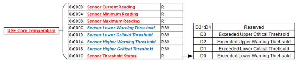
| Sensor Threshold Status | |
| Function: | Reflects which threshold has been crossed |
| Type: | unsigned binary word (32-bits) |
| Data Range: | See table below |
| Read/Write: | R |
| Initialized Value: | 0 |
| Operational Settings: | The associated bit is set when the sensor reading exceed the corresponding threshold settings. |
| Bit(s) | Description |
| D31:D4 | Reserved |
| D3 | Exceeded Upper Critical Threshold |
| D2 | Exceeded Upper Warning Threshold |
| D1 | Exceeded Lower Critical Threshold |
| D0 | Exceeded Lower Warning Threshold |
| Sensor Current Reading | |
| Function: | Reflects current reading of temperature sensor |
| Type: | Single Precision Floating Point Value (IEEE-754) |
| Data Range: | Single Precision Floating Point Value (IEEE-754) |
| Read/Write: | R |
| Initialized Value: | N/A |
| Operational Settings: | The register represents current sensor reading as a single precision floating point value. For example, for a temperature sensor, register value 0x41C6 0000 represents temperature = 24.75° Celsius. |
| Sensor Minimum Reading | |
| Function: | Reflects minimum value of temperature sensor since power up |
| Type: | Single Precision Floating Point Value (IEEE-754) |
| Data Range: | Single Precision Floating Point Value (IEEE-754) |
| Read/Write: | R |
| Initialized Value: | N/A |
| Operational Settings: | The register represents minimum sensor value as a single precision floating point value. For example, for a temperature sensor, register value 0x41C6 0000 represents temperature = 24.75° Celsius. |
| Sensor Maximum Reading | |
| Function: | Reflects maximum value of temperature/voltage/current sensor since power up |
| Type: | Single Precision Floating Point Value (IEEE-754) |
| Data Range: | Single Precision Floating Point Value (IEEE-754) |
| Read/Write: | R |
| Initialized Value: | N/A |
| Operational Settings: | The register represents maximum sensor value as a single precision floating point value. For example, for a temperature sensor, register value 0x41C6 0000 represents temperature = 24.75° Celsius. |
| Sensor Lower Warning Threshold | |
| Function: | Reflects lower warning threshold of temperature sensor |
| Type: | Single Precision Floating Point Value (IEEE-754) |
| Data Range: | Single Precision Floating Point Value (IEEE-754) |
| Read/Write: | R/W |
| Initialized Value: | Default lower warning threshold (value dependent on specific sensor) |
| Operational Settings: | The register represents sensor lower warning threshold as a single precision floating point value. For example, for a temperature sensor, register value 0xC220 0000 represents temperature = -40.0° Celsius. |
| Sensor Lower Critical Threshold | |
| Function: | Reflects lower critical threshold of temperature sensor |
| Type: | Single Precision Floating Point Value (IEEE-754) |
| Data Range: | Single Precision Floating Point Value (IEEE-754) |
| Read/Write: | R/W |
| Initialized Value: | Default lower critical threshold (value dependent on specific sensor) |
| Operational Settings: | The register represents sensor lower critical threshold as a single precision floating point value. For example, for a temperature sensor, register value 0xC25C 0000 represents temperature = -55.0° Celsius. |
| Sensor Upper Warning Threshold | |
| Function: | Reflects upper warning threshold of temperature sensor |
| Type: | Single Precision Floating Point Value (IEEE-754) |
| Data Range: | Single Precision Floating Point Value (IEEE-754) |
| Read/Write: | R/W |
| Initialized Value: | Default upper warning threshold (value dependent on specific sensor) |
| Operational Settings: | The register represents sensor upper warning threshold as a single precision floating point value. For example, for a temperature sensor, register value 0x42AA 0000 represents temperature = 85.0° Celsius. |
| Sensor Upper Critical Threshold | |
| Function: | Reflects upper critical threshold of temperature sensor |
| Type: | Single Precision Floating Point Value (IEEE-754) |
| Data Range: | Single Precision Floating Point Value (IEEE-754) |
| Read/Write: | R/W |
| Initialized Value: | Default upper critical threshold (value dependent on specific sensor) |
| Operational Settings: | The register represents sensor upper critical threshold as a single precision floating point value. For example, for a temperature sensor, register value 0x42FA 0000 represents temperature = 125.0° Celsius. |
Ethernet Configuration Registers
The registers in this section provide information about the Ethernet Configuration for the two ports on the board.
Important
Regardless if the board is configured for one or two Ethernet ports, the second IP address cannot be on the same Subnet as the First IP Address. The table below provides examples of valid and invalid IP Addresses and Subnet Mask Addresses.
| First Port (A) IP Address | First Port (A) Subnet Mask | Second Port (B) IP Address | Second Port (B) Subnet Mask | Result |
| 192.168.1.5 | 255.255.255.0 | 192.168.2.5 | 255.255.255.0 | Good |
| 192.168.1.5 | 255.255.0.0 | 192.168.2.5 | 255.255.0.0 | Conflict |
| 192.168.1.5 | 255.255.0.0 | 192.168.2.5 | 255.255.255.0 | Conflict |
| 10.0.0.15 | 255.0.0.0 | 192.168.1.5 | 255.255.255.0 | Good |
| Ethernet MAC Address and Ethernet Settings | |
| Function: | Specifies the Ethernet MAC Address and Ethernet Settings for the Ethernet port. |
| Type: | Two (2) unsigned binary word (32-bit) |
| Data Range: | See table. |
| Read/Write: | R |
| Operational Settings: | The Ethernet MAC Address consists of six octets. The Ethernet Settings are defined in table. |
| Bits | Description | Values |
| D31:D23 | Reserved | 0 |
| D22:D21 | Duplex | 00 = Not Specified 01 = Half Duplex 10 = Full Duplex 11 = Reserved |
| D20:D18 | Speed | 000 = Not Specified 001 = 10 Mbps 010 = 100 Mbps 011 = 1000 Mbps 100 = 2500 Mbps 101 = 10000 Mbps 110 = Reserved 111 = Reserved |
| D17 | Auto Negotiate | 0 = Enabled 1 = Disabled |
| D16 | Static IP Address | 0 = Enabled 1 = Disabled |
| Ethernet MAC Address and Ethernet Settings (Note: little-endian order in register) | |||||||||||||||
| Word 1 (Ethernet MAC Address (Octets 1-4)) (ex: aa:bb:cc:dd:ee:ff) | |||||||||||||||
| D31 | D30 | D29 | D28 | D27 | D26 | D25 | D24 | D23 | D22 | D21 | D20 | D19 | D18 | D17 | D16 |
| MAC Address Octet 4 (ex: 0xDD) | MAC Address Octet 3 (ex: 0xCC) | ||||||||||||||
| D15 | D14 | D13 | D12 | D11 | D10 | D9 | D8 | D7 | D6 | D5 | D4 | D3 | D2 | D1 | D0 |
| MAC Address Octet 2 (ex: 0xBB) | MAC Address Octet 1 (ex: 0xAA) | ||||||||||||||
| Word 2 (Ethernet MAC Address (Octets 5-6) and Ethernet Settings) | |||||||||||||||
| D31 | D30 | D29 | D28 | D27 | D26 | D25 | D24 | D23 | D22 | D21 | D20 | D19 | D18 | D17 | D16 |
| Ethernet Settings (See table) | |||||||||||||||
| D15 | D14 | D13 | D12 | D11 | D10 | D9 | D8 | D7 | D6 | D5 | D4 | D3 | D2 | D1 | D0 |
| MAC Address Octet 6 (ex: 0xFF) | MAC Address Octet 5 (ex: 0xEE) | ||||||||||||||
| Ethernet Interface Name | |
| Function: | Specifies the Ethernet Interface Name for the Ethernet port. |
| Type: | 8-character ASCII string |
| Data Range: | See table. |
| Read/Write: | R |
| Operational Settings: | The Ethernet Interface Name (eth0, eth1, etc) for the Ethernet port. |
| Ethernet Interface Name (Note: ascii string in register) (ex. “eth0”) | |||||||||||||||
| Word 1 (Bit 0-31) (ex: 0x3068 7465 = “0hte”) | |||||||||||||||
| D31 | D30 | D29 | D28 | D27 | D26 | D25 | D24 | D23 | D22 | D21 | D20 | D19 | D18 | D17 | D16 |
| ASCII Character (ex: '0' - 0x30) | ASCII Character (ex: 'h' - 0x68) | ||||||||||||||
| D15 | D14 | D13 | D12 | D11 | D10 | D9 | D8 | D7 | D6 | D5 | D4 | D3 | D2 | D1 | D0 |
| ASCII Character (ex: 't' - 0x74) | ASCII Character (ex: 'e' - 0x65) | ||||||||||||||
| Word 2 (Bit 32-63) (ex: 0x0000 0000) | |||||||||||||||
| D31 | D30 | D29 | D28 | D27 | D26 | D25 | D24 | D23 | D22 | D21 | D20 | D19 | D18 | D17 | D16 |
| ASCII Character (ex: null - 0x00) | ASCII Character (ex: null - 0x00) | ||||||||||||||
| D15 | D14 | D13 | D12 | D11 | D10 | D9 | D8 | D7 | D6 | D5 | D4 | D3 | D2 | D1 | D0 |
| ASCII Character (ex: null - 0x00) | ASCII Character (ex: null - 0x00) | ||||||||||||||
| Ethernet IPv4 Address | |
| Function: | Specifies the Ethernet IPv4 Address for the Ethernet port. |
| Type: | Three (3) unsigned binary word (32-bit) |
| Data Range: | See table. |
| Read/Write: | R |
| Operational Settings: | The Ethernet IPv4 Address consists of three parts: IPv4 Address, IPv4 Subnet Mask and IPv4 Gateway. |
| Ethernet IPv4 Address (Note: little-endian order in register) | |||||||||||||||
| Word 1 (Ethernet IPv4 Address) (ex: 0x1001 A8C0 = 192.168.1.16) | |||||||||||||||
| D31 | D30 | D29 | D28 | D27 | D26 | D25 | D24 | D23 | D22 | D21 | D20 | D19 | D18 | D17 | D16 |
| IPv4 Address Octet 4 (ex: 0x10 = 16) | IPv4 Address Octet 3 (ex: 0x01 = 1) | ||||||||||||||
| D15 | D14 | D13 | D12 | D11 | D10 | D9 | D8 | D7 | D6 | D5 | D4 | D3 | D2 | D1 | D0 |
| IPv4 Address Octet 2 (ex: 0xA8 = 168) | IPv4 Address Octet 1 (ex: 0xC0 = 192) | ||||||||||||||
| Word 2 (Ethernet IPv4 Subnet) (ex: 0x00FF FFFF = 255.255.255.0) | |||||||||||||||
| D31 | D30 | D29 | D28 | D27 | D26 | D25 | D24 | D23 | D22 | D21 | D20 | D19 | D18 | D17 | D16 |
| IPv4 Subnet Octet 4 (ex: 0x00 = 0) | IPv4 Subnet Octet 3 (ex: 0xFF = 255) | ||||||||||||||
| D15 | D14 | D13 | D12 | D11 | D10 | D9 | D8 | D7 | D6 | D5 | D4 | D3 | D2 | D1 | D0 |
| IPv4 Subnet Octet 2 (ex: 0xFF = 255) | IPv4 Subnet Octet 1 (ex: 0xFF = 255) | ||||||||||||||
| Word 3 (Ethernet IPv4 Gateway) (ex: 0x0101 A8C0 = 192.168.1.1) | |||||||||||||||
| D31 | D30 | D29 | D28 | D27 | D26 | D25 | D24 | D23 | D22 | D21 | D20 | D19 | D18 | D17 | D16 |
| IPv4 Gateway Octet 4 (ex: 0x01 = 1) | IPv4 Gateway Octet 3 (ex: 0x01 = 1) | ||||||||||||||
| D15 | D14 | D13 | D12 | D11 | D10 | D9 | D8 | D7 | D6 | D5 | D4 | D3 | D2 | D1 | D0 |
| IPv4 Gateway Octet 2 (ex: 0xA8 = 168) | IPv4 Gateway Octet 1 (ex: 0xC0 = 192) | ||||||||||||||
| Ethernet IPv6 Address | |
| Function: | Specifies the Ethernet IPv6 Address for the Ethernet port. |
| Type: | Five (5) unsigned binary word (32-bit) |
| Data Range: | See table. |
| Read/Write: | R |
| Operational Settings: | The IPv6 Prefix length indicates the network portion of an IPv6 address using the following format:
|
The following is an illustration of IPv6 addressing with IPv6 Prefix length of 64.
| 64 bits | 64 bits | ||||||
| Prefix | Interface ID | ||||||
| Prefix 1 | Prefix 2 | Prefix 3 | Subnet ID | Interface ID 1 | Interface ID 2 | Interface ID 3 | Interface ID 4 |
| Example: 2002:c0a8:101:0:7c99:d118:9058:1235/64 | |||||||
| 2002 | C0A8 | 0101 | 0000 | 7C99 | D118 | 9058 | 1235 |
| Ethernet IPv6 Address (Note: little-endian order within 32-bit and 16-bit words in register) (ex. IPv6 Address: 2002:c0a8:201:0:7c99:d118:9058:1235 IPv6 Prefix: 64) | |||||||||||||||
| Word 1 (Ethernet IPv6 Address (Prefix 1-2)) (ex:0xA8C0 0220 = 2002 C0A8) | |||||||||||||||
| D31 | D30 | D29 | D28 | D27 | D26 | D25 | D24 | D23 | D22 | D21 | D20 | D19 | D18 | D17 | D16 |
| Prefix 2 (ex: 0xA8C0 = C0A8) | |||||||||||||||
| D15 | D14 | D13 | D12 | D11 | D10 | D9 | D8 | D7 | D6 | D5 | D4 | D3 | D2 | D1 | D0 |
| Prefix 1 (ex: 0x0220 = 2002) | |||||||||||||||
| Word 2 (Ethernet IPv6 Address (Prefix 3/Subnet ID)) (ex:0x000 0201 = 0201 0000) | |||||||||||||||
| D31 | D30 | D29 | D28 | D27 | D26 | D25 | D24 | D23 | D22 | D21 | D20 | D19 | D18 | D17 | D16 |
| Subnet ID (ex: 0x0000 = 0000) | |||||||||||||||
| D15 | D14 | D13 | D12 | D11 | D10 | D9 | D8 | D7 | D6 | D5 | D4 | D3 | D2 | D1 | D0 |
| Prefix 3 (ex: 0x0201 = 0201) | |||||||||||||||
| Word 3 (Ethernet IPv6 Address (Interface ID 1-2)) (ex: 0x18D1 997C = 7C99 D118) | |||||||||||||||
| D31 | D30 | D29 | D28 | D27 | D26 | D25 | D24 | D23 | D22 | D21 | D20 | D19 | D18 | D17 | D16 |
| Interface ID 2 (ex: 0x18D1 = D118) | |||||||||||||||
| D15 | D14 | D13 | D12 | D11 | D10 | D9 | D8 | D7 | D6 | D5 | D4 | D3 | D2 | D1 | D0 |
| Interface ID 1 (ex: 0x997C = 7C99) | |||||||||||||||
| Word 4 (Ethernet IPv6 Address (Interface ID 3-4)) (ex: 0x3512 5890 = 9058 1235) | |||||||||||||||
| D31 | D30 | D29 | D28 | D27 | D26 | D25 | D24 | D23 | D22 | D21 | D20 | D19 | D18 | D17 | D16 |
| Interface ID 4 (ex: 0x3512 = 1235) | |||||||||||||||
| D15 | D14 | D13 | D12 | D11 | D10 | D9 | D8 | D7 | D6 | D5 | D4 | D3 | D2 | D1 | D0 |
| Interface ID 3 (ex: 0x5890 = 9058) | |||||||||||||||
| Word 5 (Ethernet IPv6 Prefix Length) (ex:0x0000 0040) | |||||||||||||||
| D31 | D30 | D29 | D28 | D27 | D26 | D25 | D24 | D23 | D22 | D21 | D20 | D19 | D18 | D17 | D16 |
| 0 | 0 | 0 | 0 | 0 | 0 | 0 | 0 | 0 | 0 | 0 | 0 | 0 | 0 | 0 | 0 |
| D15 | D14 | D13 | D12 | D11 | D10 | D9 | D8 | D7 | D6 | D5 | D4 | D3 | D2 | D1 | D0 |
| Prefix Length (ex: 0x0040 = 64) | |||||||||||||||
Interrupt Vector and Steering
When interrupts are enabled, the interrupt vector associated with the specific interrupt can be programmed (typically with a unique number/identifier) such that it can be utilized in the Interrupt Service Routine (ISR) to identify the type of interrupt. When an interrupt occurs, the contents of the Interrupt Vector registers is reported as part of the interrupt mechanism. In addition to specifying the interrupt vector, the interrupt can be directed (“steered”) to the native bus or to the application running on the onboard ARM processor.
Note
The Interrupt Vector and Interrupt Steering registers are mapped to the Motherboard Common Memory and these registers are associated with the Module Slot position (refer to Function Register Map).
| Interrupt Vector | |
| Function: | Set an identifier for the interrupt. |
| Type: | unsigned binary word (32-bit) |
| Data Range: | 0x0000 0000 to 0xFFFF FFFF |
| Read/Write: | R/W |
| Initialized Value: | 0 |
| Operational Settings: | When an interrupt occurs, this value is reported as part of the interrupt mechanism. |
| Interrupt Steering | |
| Function: | Sets where to direct the interrupt. |
| Type: | unsigned binary word (32-bit) |
| Data Range: | See table |
| Read/Write: | R/W |
| Initialized Value: | 0 |
| Operational Settings: | When an interrupt occurs, the interrupt is sent as specified: |
| Direct Interrupt to VME | 1 |
| Direct Interrupt to ARM Processor (via SerDes) (Custom App on ARM or NAI Ethernet Listener App) | 2 |
| Direct Interrupt to PCIe Bus | 5 |
| Direct Interrupt to cPCI Bus | 6 |
Modules Control Command Requests
| Modules Control Command Requests | |
| Function: | Provides the ability to command individual Modules to Reset, Power-down, or Power-up. |
| Type: | unsigned binary word (32-bit) |
| Data Range: | 0x0000 0000 to 0xFFFF FFFF |
| Read/Write: | R |
| Operational Settings: | The Module Control Commands registers provide the ability to request individual Modules to perform one of the following functions - Reset, Power-down, Power-up. Only one command can be requested at a time per Module. For example, one can't request a Reset and a Power-down at the same time for the same Module. Once the command is recognized and handled, the bit will be cleared. NOTE: Clearing of the command request bit only indicates the command has been recognized and initiated, it does not indicate that the command action has been completed. There is one Control Command Request register per Module. Each register is Bit-mapped as shown in the table below: |
| Bit(s) | Description |
| D31:D3 | Reserved |
| D2 | Module Power-up |
| D1 | Module Power-down |
| D0 | Module Reset |
Modules Health Monitoring Registers
| Module Communications Status | |
| Function: | Provides the ability to monitor factors may effect communication status of a Module. |
| Type: | unsigned binary word (32-bit) |
| Data Range: | 0x0000 0000 to 0xFFFF FFFF |
| Read/Write: | R |
| Operational Settings: | The Module Communications registers provide the ability to monitor factors that may effect the Communications Status of individual Modules. There is one register per Module. Each communication factor is bit mapped to the register as shown in the table below: |
| Bit(s) | Description |
| D31:D5 | Reserved |
| D4 | Module Communications Error Detected |
| D3 | Module Firmware Not Ready |
| D2 | Module LinkInit Not Done |
| D1 | Module Not Detected |
| D0 | Module Powered-down |
Module Powered-down: The user can request an individual Module be powered-down (see Module Control Command Requests). Once the request is detected and acted upon, this bit will be set. Once powered-down, you will not be able to communicate with the Module.
Module Not Detected: If a Module in this slot has not been detected, you will not be able to communicate with the Module.
Module LinkInit Not Done: Module communications is accomplished via SERDES. LinkInit is required to establish a connection to the Module. If the LinkInit has not been successfully completed, you will not be able to communicate with the Module.
Module Firmware Not Ready: Each Module has Firmware that is ready from Module QSPI and loaded for execution. If this Firmware was not loaded and started successfully, you may not be able to communicate with the Module.
Module Communications Error Detected: If at some point during run-time, communications with the Module has failed, this bit will be set.
| Module BIT Status | |
| Function: | Provides the ability to monitor the individual Module BIT Status. |
| Type: | unsigned binary word (32-bit) |
| Data Range: | 0x0000 0000 to 0xFFFF FFFF |
| Read/Write: | R |
| Operational Settings: | The Module BIT Status registers provide the ability to monitor individual Module BIT results as Latched and current value. A 1 is any bit field indicates BIT failure for the Module in that slot. |
| Bit(s) | Description |
| D31:D19 | Reserved |
| D18 | Module Slot 2 BIT Failure (current value) |
| D17 | Module Slot 1 BIT Failure (current value) |
| D16 | Reserved |
| D15:D3 | Reserved |
| D2 | Module Slot 2 BIT Failure - Latched |
| D1 | Module Slot 1 BIT Failure - Latched |
| D0 | Reserved |
Scratchpad Area
| Scratchpad Area | |
| Function: | Registers reserved as scratch pad for customer use |
| Type: | unsigned binary word (32-bit) |
| Data Range: | 0x0000 0000 to 0xFFFF FFFF |
| Read/Write: | R/W |
| Operational Settings: | This area in memory is reserved for customer use or POST FRAM results. |
MOTHERBOARD FUNCTION REGISTER MAP
KEY
| Configuration/Control |
| Measurement/Status/Board Information |
| MODULE INFORMATION REGISTERS | |||||
| OFFSET | REGISTER NAME | ACCESS | OFFSET | REGISTER NAME | ACCESS |
| 0x03FC | Module Slot Addressing Ready | R | |||
| 0x0400 | Module Slot 1 Address | R | 0x0430 | Module Slot 1 Size | R |
| 0x0404 | Module Slot 2 Address | R | 0x0434 | Module Slot 2 Size | R |
| 0x0460 | Module Slot 1 ID | R | |||
| 0x0464 | Module Slot 2 ID | R | |||
| HARDWARE INFORMATION REGISTERS | |||||
| OFFSET | REGISTER NAME | ACCESS | OFFSET | REGISTER NAME | ACCESS |
| 0x0020 | Product Serial Number | R | |||
| 0x0024 | Platform | R | 0x0030 | Processor Count/Ethernet Count | R |
| 0x0028 | Model | R | 0x0034 | Maximum Module Slot Count/ARM Platform Type | R |
| 0x002C | Generation | R | |||
| 0x0038 | Processor Platform (Bit 0-31) | R | 0x0040 | Processor Operating System (Bit 0-31) | R |
| 0x003C | Processor Platform (Bit 32-63) | R | 0x0044 | Processor Operating System (Bit 32-63) | R |
| 0x0048 | Processor Operating System (Bit 64-95) | R | |||
| 0x004C | Processor Operating System Version (Bit 0-31) | R | |||
| 0x0050 | Processor Operating System Version (Bit 32-63) | R | |||
| MOTHERBOARD FIRMWARE INFORMATION REGISTERS | |||||
| OFFSET | REGISTER NAME | ACCESS | OFFSET | REGISTER NAME | ACCESS |
| Motherboard Core Information | Motherboard FPGA Information | ||||
| 0x0100 | MB Core Major/Minor Version | R | 0x0270 | MB FPGA Revision | R |
| 0x0104 | MB Core Minor 2/3 Version | R | 0x0274 | MB FPGA Compile Date/Time | R |
| 0x0108 | MB Core Build Date (Bit 0-31) | R | |||
| 0x010C | MB Core Build Date (Bit 32-63) | R | |||
| MOTHERBOARD MEASUREMENTS REGISTERS | |||||
| OFFSET | REGISTER NAME | ACCESS | OFFSET | REGISTER NAME | ACCESS |
| Temperature Readings | High Precision Temperature Readings | ||||
| 0x0200 | Current UltraScale Temperatures | R | 0x0230 | Current UltraScale Core Temperature | R |
| 0x0204 | Reserved | R | 0x0234 | Current Motherboard PCB Temperature | R |
| 0x0208 | Max UltraScale Temp | R | |||
| 0x020C | Reserved | R | |||
| 0x0210 | Min UltraScale Temperatures | R | |||
| 0x0214 | Reserved | R | |||
| MOTHERBOARD HEALTH MONITORING REGISTERS | |||||
| OFFSET | REGISTER NAME | ACCESS | OFFSET | REGISTER NAME | ACCESS |
| 0x20F8 | Motherboard Sensor Summary Status | R | |||

| ETHERNET CONFIGURATION REGISTERS | |||||
| OFFSET | REGISTER NAME | ACCESS | OFFSET | REGISTER NAME | ACCESS |
| Ethernet A | Ethernet B | ||||
| 0x0070 | Ethernet A MAC (Octets 1-4) | R | 0x00A0 | Ethernet B MAC (Octets 1-4) | R |
| 0x0074 | Ethernet A MAC (Octets 5-6)/Misc Settings | R | 0x00A4 | Ethernet B MAC (Octets 5-6)/Misc Settings | R |
| 0x0078 | Ethernet A Interface Name (Bit 0-31) | R | 0x00A8 | Ethernet B Interface Name (Bit 0-31) | R |
| 0x007C | Ethernet A Interface Name (Bit 32-63) | R | 0x00AC | Ethernet B Interface Name (Bit 32-63) | R |
| 0x0080 | Ethernet A IPv4 Address | R | 0x00B0 | Ethernet B IPv4 Address | R |
| 0x0084 | Ethernet A IPv4 Subnet Mask | R | 0x00B4 | Ethernet B IPv4 Subnet Mask | R |
| 0x0088 | Ethernet A IPv4 Gateway | R | 0x00B8 | Ethernet B IPv4 Gateway | R |
| 0x008C | Ethernet A IPv6 Address (Prefix 1-2) | R | 0x00BC | Ethernet B IPv6 Address (Prefix 1-2) | R |
| 0x0090 | Ethernet A IPv6 Address (Prefix 3/Subnet ID) | R | 0x00C0 | Ethernet B IPv6 Address (Prefix 3/Subnet ID) | R |
| 0x0094 | Ethernet A IPv6 Address (Interface ID 1-2) | R | 0x00C4 | Ethernet B IPv6 Address (Interface ID 1-2) | R |
| 0x0098 | Ethernet A IPv6 Address (Interface ID 3-4) | R | 0x00C8 | Ethernet B IPv6 Address (Interface ID 3-4) | R |
| 0x009C | Ethernet A IPv6 Prefix Length | R | 0x00CC | Ethernet B IPv6 Prefix Length | R |
| INTERRUPT REGISTERS | |||||
| OFFSET | REGISTER NAME | ACCESS | OFFSET | REGISTER NAME | ACCESS |
| 0x0500 - 0x057C | Module 1 Interrupt Vector 1 - 32 | R/W | 0x0600 - 0x067C | Module 1 Interrupt Steering 1 - 32 | R/W |
| 0x0700 - 0x077C | Module 2 Interrupt Vector 1 - 32 | R/W | 0x0800 - 0x087C | Module 2 Interrupt Steering 1 - 32 | R/W |
| MODULE CONTROL COMMAND REQUEST REGISTERS | |||||
| OFFSET | REGISTER NAME | ACCESS | OFFSET | REGISTER NAME | ACCESS |
| 0x01D8 | Module Slot 1 Command Request | R | |||
| 0x01DC | Module Slot 2 Command Request | R | |||
| MODULES HEALTH MONITORING REGISTERS | |||||
| OFFSET | REGISTER NAME | ACCESS | OFFSET | REGISTER NAME | ACCESS |
| 0x01B8 | Module Slot 1 Communications Status | R | 0x0128 | Module BIT Status (current and latched) | R |
| 0x01BC | Module Slot 2 Communications Status | R | |||
| SCRATCHPAD REGISTERS | |||||
| OFFSET | REGISTER NAME | ACCESS | OFFSET | REGISTER NAME | ACCESS |
| 0x3800 - 0x3BFF | Scratchpad Registers | R/W | |||
ETHERNET
(For detailed supplement, please visit the NAI web-site specific product page and refer to: Ethernet Interface for Generation 5 SBC and Embedded IO Boards Specification)
Note
For products capable of 10/100/1000Base-KX functionality – the product Ethernet PHY supports 1000BASE-X. Product interoperability with 10/100/1000BASE-KX is supported with 1000BASE-X (provided that auto-negotiation is disabled).
The Ethernet Interface Option allows communications and control access to all function modules either via the system BUS or Ethernet ports 1 or 2.
| Ethernet 1 | Ethernet 2 | Ethernet 3* | Ethernet 4* | |
| (REF PORT A) | (REF PORT B) | (REF PORT C) | (REF PORT D) | |
| The default IP address: | 192.168.1.16 | 192.168.2.16 | 192.168.3.16 | 192.168.4.16 |
| The default subnet: | 255.255.255.0 | 255.255.255.0 | 255.255.255.0 | 255.255.255.0 |
| The default gateway: | 192.168.1.1 | 192.168.2.1 | 192.168.3.1 | 192.168.4.1 |
*see Part Number Designation for applicability.
Note
Actual “as shipped” card Ethernet default IP addresses may vary based upon final ATP configuration(s).
The NAI interface supports IPv4 and IPv6 and both the TCP and UDP protocols. The Ethernet Operation Mode Command Listener application running on the motherboard host processor implements the operation interface. The listener is operational on startup through the nai_MBStartup process and listen on specific ports for commands to process. The default ports are listed below:
- TCP1 - Port 52801
- TCP2 - Port 52802
- UDP1 - Port 52801
- UDP2 - Port 52802
While the listener is active, note that interrupts from the motherboard do not trigger. The listener can be disabled by turning off the nai_MBStartup process through the Motherboard EEPROM. To turn off nai_MBStartup use the command mbeeprom_util set MBStartupInitOnlyFlag 1 in the console, either by serial port or telnet to the motherboard, and then reboot the system. To turn on the nai_MBStartup use the command mbeeprom_util set MBStartupInitOnlyFlag 0 in the console, either by serial port or telnet to the motherboard, and then reboot the system.
Ethernet Message Framework
The interface uses a specific message framework for all commands and responses. All messages begin with a Preamble code and end with a Postamble code. The message framework is shown below.
| Preamble 2 bytes Always 0xD30F | SequenceNo 2 bytes | Type Code 2 byte | Message Length (2 bytes) | Payload (0..1414 bytes) | Postamble 2 bytes Always 0xF03D |
Message Elements
| Preamble | The Preamble is used to delineate the beginning of a message frame. The Preamble is always 0xD30F. |
| SequenceNo | The SequenceNo is used to associate Commands with Responses. |
| Type Code | Type Codes are used to define the type of Command or Response the message contains. |
| Message Length | The Message Length is the number of bytes in the complete message frame starting with and including the Preamble and ending with and including the Postamble. |
| Payload | The Payload contains the unique data that makes up the command or response. Payloads vary based on command type. |
| Postamble | The Postamble is use to delineate the end of a message frame. The Postamble is always 0xF03D. |
Notes
- The messaging protocol applies only to card products.
- Messaging is managed by the connected (client) computer. The client computer will send a single message and wait for a reply from the card. Multiple cards may be managed from a single computer, subject to channel and computer capacity.
Board Addressing
The interface provides two main addressing areas: Onboard and Off-board.
Onboard addressing refers to accessing resources located on the board that is implementing the operation interface (including its modules).
Off-board addressing refers to accessing resources located on another board reachable via VME, PCI, or other bus. Off-board addressing requires a Master/Slave configuration.
The user must always specify if a particular address is Onboard or Off-board. See the command descriptions for the onboard and off-board flags.
Within a particular board (Onboard or Off-board), the address space is broken up into two areas: Motherboard Common Address Space and Module Address Space. All addresses are 32-bit.
Motherboard Common Address Space starts at 0x00000000 and ends at 0x00004000. This is a 4Kx32-bit address space (16 kbytes).
Module Address Space starts at 0x00004000. Module addressing is dynamically configured at startup. NAI boards support between 1 and 6 modules. The minimum module address space size is 4Kx32 (16 kbytes) and module sizes are always a multiple of 4Kx32.
Module addressing is dynamic and cumulative. The first detected module (starting with Slot 1) is given an address of 0x00004000. The 2nd detected Module is given an address of:
First_Detected_Module_Address + First_Detected_Module_Size
Note
Slots do not define addresses.
If no module is detected in a module slot, that slot is not given an address. Therefore, if the first detected Module is in Slot 2, then that module address will be 0x00004000. If the next detected module is in Slot 4, then the address of that Module will be:
Second_Detected_Module_Address = First_Detected_Module_Address + First_Detected_Module_Size
If a 3rd Module is detected in Slot 6, then the address of that Module will be:
Third_Detected_Module_Address = Second_Detected_Module_Address + Second_Detected_Module_Size
Note
Module addresses are calculated at each board startup when the modules are detected. Therefore, if a module should fail to be detected due to malfunction or because it was removed from the motherboard, the addresses of the modules that follow it in the slot sequence will be altered. This is important to note when programming to this interface.
Users can always retrieve the Module Addresses, Module Sizes and Module IDs from the fixed Motherboard Common address area. This data is set upon each board startup. While the Module Addressing is dynamic, the address where these addresses are stored is fixed. For example, to find the startup address of the module location in Slot 3, refer to the MB Common Address 0x00000408 from the Motherboard Common Addresses table that follows.
Ethernet Wiring Convention
| RJ-45 Pin | T568A Color | T568B Color | 10/100Base-T | 1000BASE-T | NAI wiring convention |
| 1 | white/green stripe | white/orange stripe | TX+ | DA+ | ETH-TP0+ |
| 2 | green | orange | TX- | DA- | ETH-TP0- |
| 3 | white/orange stripe | white/green stripe | RX+ | DB+ | ETH-TP1+ |
| 4 | blue | blue | DC+ | ETH-TP2+ | |
| 5 | white/blue stripe | white/blue stripe | DC- | ETH-TP2- | |
| 6 | orange | green | RX- | DB- | ETH-TP1- |
| 7 | white/brown stripe | white/brown stripe | DD+ | ETH-TP3+ | |
| 8 | brown | brown | DD- | ETH-TP3- |
NIU2U I/O MAPPING
NIU2U I/O Mapping (for reference) is shown below, with respect to DATAIO. Additional information on pin-outs can be found in the Module Operational Manuals or by contacting the factory (NOTE: ‘N/C’ indicates pin not available at Jx I/O connector).
| Internal Reference Only | MOD1 (J2 - I/O) | MOD2 (J4 - I/O) |
| MOD-DATIO01 | 24 | 51 |
| MOD-DATIO02 | 23 | 58 |
| MOD-DATIO03 | 22 | 53 |
| MOD-DATIO04 | 21 | 52 |
| MOD-DATIO05 | 16 | 59 |
| MOD-DATIO06 | 15 | 64 |
| MOD-DATIO07 | 9 | 46 |
| MOD-DATIO08 | 8 | 45 |
| MOD-DATIO09 | 14 | 38 |
| MOD-DATIO10 | 13 | 44 |
| MOD-DATIO11 | 7 | 29 |
| MOD-DATIO12 | 6 | 43 |
| MOD-DATIO13 | 3 | 61 |
| MOD-DATIO14 | 2 | 60 |
| MOD-DATIO15 | 38 | 55 |
| MOD-DATIO16 | 29 | 54 |
| MOD-DATIO17 | 28 | 47 |
| MOD-DATIO18 | 27 | 48 |
| MOD-DATIO19 | 20 | 40 |
| MOD-DATIO20 | 19 | 39 |
| MOD-DATIO21 | 12 | 31 |
| MOD-DATIO22 | 11 | 30 |
| MOD-DATIO23 | 5 | 66 |
| MOD-DATIO24 | 1 | 65 |
| MOD-DATIO25 | 37 | 22 |
| MOD-DATIO26 | 36 | 21 |
| MOD-DATIO27 | 46 | 14 |
| MOD-DATIO28 | 45 | 15 |
| MOD-DATIO29 | 53 | 63 |
| MOD-DATIO30 | 52 | 62 |
| MOD-DATIO31 | 4 | 57 |
| MOD-DATIO32 | 10 | 56 |
| MOD-DATIO33 | 18 | 50 |
| MOD-DATIO34 | 17 | 49 |
| MOD-DATIO35 | 26 | 42 |
| MOD-DATIO36 | 25 | 41 |
| MOD-DATIO37 | 35 | 33 |
| MOD-DATIO38 | 34 | 32 |
| MOD-DATIO39 | 44 | 24 |
| MOD-DATIO40 | 43 | 23 |
| N/C | ||
| N/C | ||
| N/C | ||
| SYSTEM-GND | 51 | 9 |
| SYSTEM-GND | 58 | 16 |
NIU2U PART NUMBER DESIGNATION
| Standard Product: NIU2U-AAABBBPIDC0H-XX |
|---|
| PROD ID | M1 | M2 | P | MEM | OBIO | SW/OS | RES | RES | (-XX) | Configuration and Option Descriptions |
| NIU2U- | Xilinx Zynq UltraScale SoC 2x 10/100/1000BASE-T Ethernet 2x COSA Module Slots | |||||||||
| AAA | Function Module Slot 1 (M1) Z00 = No Module | |||||||||
| BBB | Function Module Slot 2 (M2) Z00 = No Module | |||||||||
| P | Processor Type (Local processing requires OS) 1 = Dual-core Arm® Cortex®-A53 MPCore @ 1.2 GHz 2 = Quad-core Arm® Cortex®-A53 MPCore @ 1.2 GHz | |||||||||
| I | On-board Memory Support (DDR4 SDRAM / SATA SSD) 1 = 4 GB LPDDR4 / 40 GB | |||||||||
| D | On-board I/O 1 = 2 x 10/100/1000 Base-T & USB 2.0(default) 2 = Reserved 3 = TSN capable, 2x 10/100/1000 (Pending) | |||||||||
| C | Processor / OS (Note 1) (OS options are applicable w/ ARM processor access only) 0 = Remote Ethernet Server (RES) 1 = PetaLinux 2023.2 (default) 2 = BIT / PetaLinux 2023.2 (Pending) 3 -5 = Reserved 6 = BIT / VxWorks 7 (Pending) 7 = U-Boot (for VxWorks 7) A = Deos 653 (Pending) | |||||||||
| 0 | Fiber Optic 0 = (default) 1 = 2x 100/1000 Base-SR | |||||||||
| H | Power Supply Hold-up (HU) 0 = No HU (default) H = HU Installed | |||||||||
| XX | Special Option Code (assigned at factory, or leave blank) |
| 1. | 0= RES; Remote server (listener application) installed - Ethernet communications via NAI Ethernet Protocol. Otherwise, select desired OS w/ARM processor access (user application capable). |
| 2. | NAI P/N: NIU2U-CONN-KIT; Mating Connector Kit: The mating connector kit includes 1 each (or equivalent): J1 Mate: NAI P/N: 05-0297-COM D38999/26WA98SA / 3-pin, A-key J2 Mate: NAI P/N: 05-0284-COM D38999/26WF35PN / 66-pin, N-key J3 Mate: NAI P/N: 05-0302-COM D38999/26WD35PN / 37-pin, N-key J4 Mate: NAI P/N: 05-0285-COM |
SYNCHRO/RESOLVER AND LVDT/RVDT SIMULATION MODULE CODE TABLES
Select the Digital-to-Synchro (DSx), Digital-to-Resolver (DRx) or Digital-to-LVDT/RVDT (DLx) module ID corresponding to the application operating parameters required from the following code table (where x = the specific module ID designator). Customer should indicate the actual frequency applicable the design to assure that the correct default band width is set at the factory. All Input and Reference voltages are auto ranging. Frequency/voltage band tolerances +/- 10%. For availability and ranges other than those listed contact the factory. Specifications may be subject to change.
- Single Channel module pending availability (contact factory)
| Module ID | Format | Channel(s) | Output Voltage VL-L (Vrms) | Reference Voltage (Vrms) | Frequency Range (Hz) | Power / CH maximum (VA) | Notes |
| DS1 | SYN | 1* | 2 - 28 | 2 - 115 | 47 - 1 K | 3 | |
| DR1 | RSL | ||||||
| DL1 | LVDT/RVDT | ||||||
| DS2 | SYN | 1* | 2 - 28 | 2 - 115 | 1 K - 5 K | 3 | |
| DR2 | RSL | ||||||
| DL2 | LVDT/RVDT | ||||||
| DS3 | SYN | 1* | 2 - 28 | 2 - 115 | 5 K - 10 K | 3 | |
| DR3 | RSL | ||||||
| DL3 | LVDT/RVDT | ||||||
| DS4 | SYN | 1* | 2 - 28 | 2 - 115 | 10 K - 20 K | 3 | |
| DR4 | RSL | ||||||
| DL4 | LVDT/RVDT | ||||||
| DS5 | SYN | 1* | 28 - 90 | 2 - 115 | 47 - 1 K | 3 | |
| DR5 | RSL | ||||||
| DL5 | LVDT/RVDT | ||||||
| DSX | SYN | 1* | X | X | X | X | X = TBD; special configuration, requires special part number code designation, contact factory |
| DRX | RSL | ||||||
| DLX | LVDT/RVDT | ||||||
| DSA | SYN | 2 | 2 - 28 | 2 - 115 | 47 - 1 K | 1.5 | |
| DRA | RSL | ||||||
| DLA | LVDT/RVDT | ||||||
| DSB | SYN | 2 | 2 - 28 | 2 - 115 | 1 K - 5 K | 1.5 | |
| DRB | RSL | ||||||
| DLB | LVDT/RVDT | ||||||
| DSC | SYN | 2 | 2 - 28 | 2 - 115 | 5 K - 10 K | 1.5 | |
| DRC | RSL | ||||||
| DLC | LVDT/RVDT | ||||||
| DSD | SYN | 2 | 2 - 28 | 2 - 115 | 10 K - 20 K | 1.5 | |
| DRD | RSL | ||||||
| DLD | LVDT/RVDT | ||||||
| DSE | SYN | 2 | 28 - 90 | 2 - 115 | 47 - 1 K | 2.2 | |
| DRE | RSL | ||||||
| DLE | LVDT/RVDT | ||||||
| DSY | SYN | 2 | Y | Y | Y | Y | Y = TBD; special configuration, requires special part number code designation, contact factory |
| DRY | RSL | ||||||
| DLY | LVDT/RVDT | ||||||
| DSJ | SYN | 3 | 2 - 28 | 2 - 115 | 47 - 1 K | 0.5 | |
| DRJ | RSL | ||||||
| DLJ | LVDT/RVDT | ||||||
| DSK | SYN | 3 | 2 - 28 | 2 - 115 | 1 K - 5 K | 0.5 | |
| DRK | RSL | ||||||
| DLK | LVDT/RVDT | ||||||
| DSL | SYN | 3 | 2 - 28 | 2 - 115 | 5 K - 10 K | 0.5 | |
| DRL | RSL | ||||||
| DLL | LVDT/RVDT | ||||||
| DSM | SYN | 3 | 2 - 28 | 2 - 115 | 10 K - 20 K | 0.5 | |
| DRM | RSL | ||||||
| DLM | LVDT/RVDT | ||||||
| DSN | SYN | 3 | 28 - 90 | 2 - 115 | 47 - 1 K | 0.5 | |
| DRN | RSL | ||||||
| DLN | LVDT/RVDT | ||||||
| DSZ | SYN | 3 | Z | Z | Z | Z | Z = TBD; special configuration, requires special part number code designation, contact factory |
| DRZ | RSL | ||||||
| DLZ | LVDT/RVDT |
SYNCHRO/RESOLVER AND LVDT/RVDT MEASUREMENT MODULE CODE TABLES
SYN/RSL Four-Channel Measurement (Field Programmable SYN/RSL)
Select the Synchro/Resolver-to-Digital (SDx) module ID corresponding to the application operating parameters required from the following code table (where x = the specific module ID designator). Customer should indicate the actual frequency applicable to the design to assure that the correct default band width is set at the factory. All Input and Reference voltages are auto ranging. For availability and ranges other than those listed contact the factory. Specifications may be subject to change.
Frequency/voltage band tolerances +/- 10%.
| Module ID | Input Voltage V (Vrms) | Reference Voltage + (Vrms) | Frequency Range + (Hz) | Notes |
| SD1 | 2 - 28 | 2 - 115 | 47 - 1 K | |
| SD2 | 2 - 28 | 2 - 115 | 1K - 5 K | |
| SD3 | 2 - 28 | 2 - 115 | 5K - 10 K | |
| SD4* | 2 - 28 | 2 - 115 | 10K - 20 K | |
| SD5 | 28 - 90 | 2 - 115 | 47 - 1 K | |
| SDX* | X | X | X | X = TBD; special configuration, requires special part number code designation, contact factory |
*Consult factory for availability
LVDT/RVDT Four-Channel Measurement (Field Programmable 2, 3 or 4-Wire)
Select the LVDT/RVDT-to-Digital (LDx) module ID corresponding to the application operating parameters required from the following code table (where x = the specific module ID designator). Customer should indicate the actual frequency applicable to the design to assure that the correct default band width is set at the factory. All Input and Excitation voltages are auto ranging. For availability and ranges other than those listed contact the factory. Specifications may be subject to change.
Frequency/voltage band tolerances +/- 10%.
| Module ID | Input Signal Voltage V (Vrms) | Excitation Voltage (Vrms) | Frequency Range (Hz) | Notes |
| LD1 | 2 - 28 | 2 - 115 | 47 - 1 K | |
| LD2 | 2 - 28 | 2 - 115 | 1K - 5 K | |
| LD3 | 2 - 28 | 2 - 115 | 5K - 10 K | |
| LD4* | 2 - 28 | 2 - 115 | 10K - 20 K | |
| LD5 | 28 - 90 | 2 - 115 | 47 - 1 K | |
| LDX* | X | X | X | X = TBD; special configuration, requires special part number code designation, contact factory |
*Consult factory for availability
REVISION HISTORY
| Revision Date | Description |
|---|---|
| 2026-09-30 | Initial publication of NIU2U manual. |
NAI Cares
North Atlantic Industries (NAI) is a leading independent supplier of Embedded I/O Boards, Single Board Computers, Rugged Power Supplies, Embedded Systems and Motion Simulation and Measurement Instruments for the Military, Aerospace and Industrial Industries. We accelerate our clients’ time-to-mission with a unique approach based on a Configurable Open Systems Architecture™ (COSA®) that delivers the best of both worlds: custom solutions from standard COTS components.
We have built a reputation by listening to our customers, understanding their needs, and designing, testing and delivering board and system-level products for their most demanding air, land and sea requirements. If you have any applications or questions regarding the use of our products, please contact us for an expedient solution.
Please visit us at: www.naii.com or select one of the following for immediate assistance:
Documentation
FAQ
Application Notes
http://www.naii.com/applicationnotes
Calibration and Repairs
http://www.naii.com/calibrationrepairs
Call Us
(631) 567-1100
Link to original