
68SR1 DATA SHEET
Solid-State Power Switch Output; 3-Modules supporting up to 4-Channels each
The 68SR1 3U OpenVPX configurable open systems architecture motherboard can be configured with up to three NAI Solid-State Power Controller/Relay (switching) modules, each capable of supporting up to four isolated high current & voltage discrete output switching channels. External command and control is provided via one PCIe x1 backplane interface and one Ethernet port, which can be factory configured to support 10/100/1000BASE-T or 1000BASE-X. Ideally suited for rugged Mil-Aero applications, the 68SR1 delivers off-the-shelf solutions that accelerate deployment of SWaP-optimized systems in air, land and sea applications.
The board platform provides support for (3) different NAI solid-state power controller switching relay function module types:
| Module ID / Type | # of Channels | Description |
|---|---|---|
| SW1 | 4 | Normally Open (NO), Low-V, ±100V @ 6A continuous (max./Ch.) |
| SW2 | 4 | Normally Open (NO), High-V, ±200V @ 4A continuous (max./Ch.) |
| SW3 | 2 | Normally Closed (NC), Low-V, ±100V @ 3A continuous (max./Ch.) |
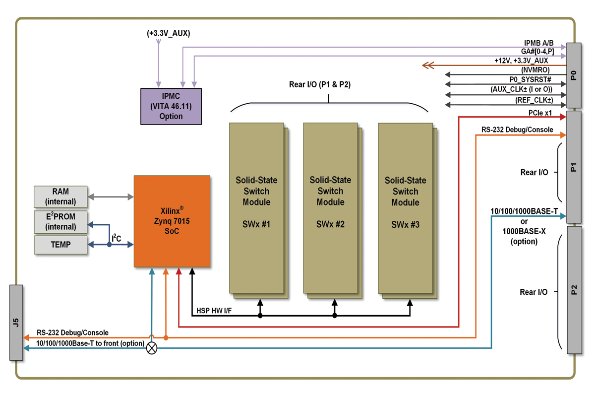
68SR1 Simplified Block Diagram
Features Summary
|
3U OpenVPX Profile supported
Data and Control Interfaces
IPMC support (configured option)
|
Supports 3 independent Solid-State SWx modules
Rear I/O utilized standard VPX connectors RS-232 debug/console port |
Software Support Kit (SSK) Provided
Commercial or Rugged Applications
|
Specifications*
Motherboard
| Signal Logic Level: | Supports PCIe ver. 2.0 bus (x1) |
| Power (Motherboard): | 12 V (VS1) @ 225 mA (does not include load power) 3.3V_AUX @ 98 mA (max) Then add power for each individual SWx module |
| Temperature, Operating: | “C” = 0°C to +70°C, “H” = -40°C to +85°C (see part number) Each board is cycled from -40°C to +85°C (option “H”) |
| Storage Temperature: | -55°C to +105°C |
| General size: | Height: 3.94” / 100 mm (3U) Width: 0.8” / 20.3 mm (4HP) conduction cooled with wedgelocks or front panel air-cooled option or 1.0” / 25.4 mm (5HP) front panel air-cooled option Depth: 6.3” / 160 mm deep |
| Weight (est.): | 8.5 oz. (241 g) unpopulated (approx.) (convection or conduction cooled) >> then add weight for each module (typically 2.5 oz. (71 g) each) |
Solid-State Power Controller Relay Switch Module Details
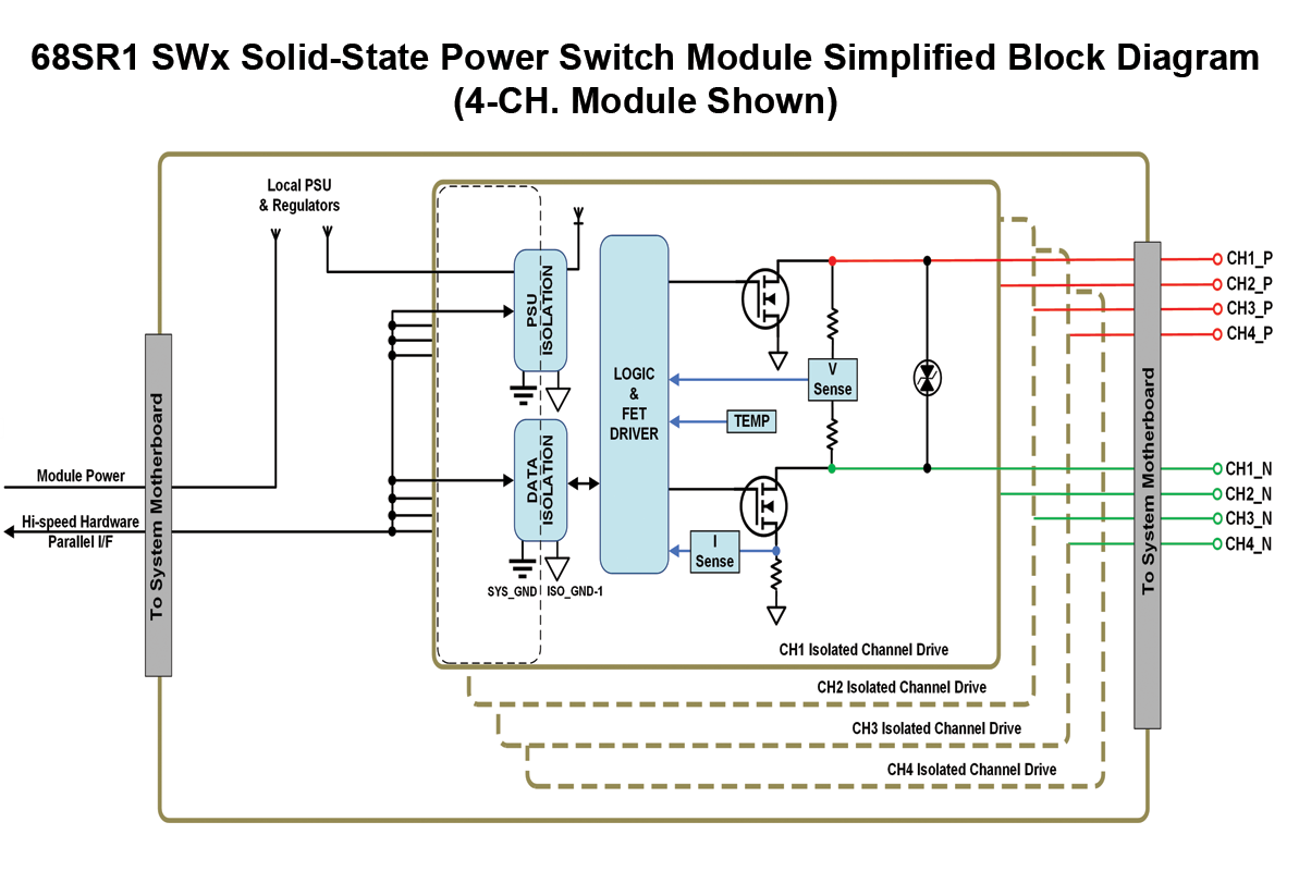
68SR1 SWx (4-Ch.) Solid-State Power Switch Module Simplified Block Diagram
Module Characteristics / Module Type
| Module ID: | Channels: | Description / Default Type, Voltage Range @ Current (max./Ch.): |
|---|---|---|
| SW1 | 4 | Normally Open (NO) / Low-V, ±100V @ 6A continuous |
| SW2 | 4 | Normally Open (NO), High-V, ±200V @ 4A continuous |
| SW3 | 2 | Normally Closed (NC), Low-V, ±100V @ 3A continuous |
| Overvoltage Surge Protection: | 15% Rated VDC max. (clamped) |
| Output Mode Format: (programmable per channel) | Command Output Drive = OPEN or CLOSED |
| Channel OPEN Output Impedance: | High-Z (>1 MΩ) |
| Channel CLOSED Output Impedance: | <0.1 Ω |
| System Protection: | All output(s) are set to “Default” (at Power-ON and reset). No voltage transients on power-on or power-off. |
| Load & Channel Protection: | Short circuit protected. Channel shuts “off” and a flag is set when current exceeds programmable overcurrent setting (max 6A) > 10ms. Channel over-current reset by control/status register command. |
| Open-Switch Voltage Measurement: | Voltage: LSB = 100 mV; Accuracy: ±1V |
| Closed-Switch Current Measurement: | User can read current of each channel. Current: LSB = 20 mA; Accuracy: ±100 mA |
| Parallel Operation: | All channels (within the module) can be paralleled for current share. (pending) |
| Isolation: | Module power source (ISO-GND) and I/O to system ground is ≥500 VDC |
| Power: | SW1: 12 VDC / 320 mA (max) (does not include source powered load) SW2: 12 VDC / 320 mA (max) (does not include source powered load) SW3: 12 VDC / 160 mA (max) (does not include source powered load) |
| Weight (est.): | SW1: 2.5 oz. (71 g) SW2: 2.5 oz. (71 g) SW3: 2.5 oz. (71 g) |
*(All) specifications pending design verifications and qualification. Specifications listed are defined at/to the module boundary.
All specifications are subject to change without notice. All product and company names are trademarks or registered trademarks of their respective holders.
INTRODUCTION
NAI is a leading manufacturer of rugged embedded boards, including the 68SR1 3U OpenVPX Solid-State Power Controller Relay Board. The 68SR1 is a configurable open systems architecture (COSA®) motherboard that can be populated with up to three NAI Solid-State Power Controller/Relay (SWx) switching modules, each supporting up to four isolated, high-current and high-voltage discrete output switching channels. Three module types are available:
* SW1 (4-channel, normally open, ±100 V @ 6 A)
* SW2 (4-channel, normally open, ±200 V @ 4 A)
* SW3 (2-channel, normally closed, ±100 V @ 3 A)
Each module provides continuous background Built-In-Test (BIT), per-channel voltage and current measurement, programmable overcurrent protection, and ≥500 VDC isolation between the module power source and system ground. External command and control is provided through a PCIe x1 backplane interface and a single Ethernet port, factory-configurable for 10/100/1000BASE-T or 1000BASE-X, with an optional VITA 46.11 IPMC. Available in air-cooled and conduction-cooled configurations with commercial and extended temperature ranges, the 68SR1 meets the rigorous demands of military and aerospace applications and delivers an off-the-shelf solution that accelerates deployment of SWaP-optimized systems in air, land, and sea platforms.
68SR1 Overview
The 68SR1 3U OpenVPX Solid-State Power Controller Relay Board offers a variety of features designed to meet the needs of complex and time-critical sense and response requirements for I/O-intensive, mission-critical applications. Key features of the 68SR1 include:
- 3U Profiles supported: This board is compatible with both VPX and OpenVPX standards, with module and slot profiles specified as MOD3- PER-1U-16.3.3-2 and SLT3-PER-1U-14.3.3, respectively. This allows for interoperability with a wide range of systems.
- PCIe (x1): The board features PCIe (x1) connectivity for fast and efficient data transfer.
- Control via Gig-E or PCIe interface: The 68SR1 provides easy integration into a system by way of Gig-E or PCIe interface control capability. Gig-E interface is ideal for systems requiring high-speed communication, while PCIe interface is an excellent option for data-intensive applications.
- Support for three solid-state power controller/relay modules: The board can support up to three NAI Solid-State Power Controller/Relay (switching) modules. Each module is capable of supporting up to four isolated high current and voltage discrete output switching channels. Continuous Background Built-In-Test (BIT) continually checks and reports on the health of each channel, allowing for preventative maintenance and reducing the likelihood of downtime.
- 1x 10/100/1000Base-T or 1000Base-X Ethernet: The board has one 10/100/1000Base-T or 1000Base-X Ethernet port, with the option to have the port to the rear or to the front I/O. This port provides enhanced data communication capabilities and faster network connectivity for advanced control and data acquisition applications.
- RS-232 debug/console port: An RS-232 debug/console port (front and rear) that provides a standard interface for communicating with the board for maintenance and debugging purposes. This serial port can be used for configuring the board or accessing diagnostic information and logs.
- Intelligent I/O library support included: The 68SR1 comes with intelligent I/O library support to help manage and control the I/O capabilities of the board.
- Background Built-In-Test (BIT): The board’s BIT continually checks and reports on the health of each channel, allowing for preventative maintenance and reducing the likelihood of downtime.
- Software Support Kits (SSKs) and drivers available: SSKs and drivers are available to make the board easier to integrate into a system and develop software.
- Commercial and rugged models: The 68SR1 is available in both commercial and rugged models, making it suitable for a wide range of applications.
- Operating temperature: The board has a wide operating temperature range, with a commercial model operating from 0° C to 70° C, and a rugged model operating from -40° C to +85° C. This makes it suitable for use in a wide range of environments.
Overall, the 68SR1 3U OpenVPX Solid-State Power Controller Relay Board is a reliable and versatile solution for demanding computing environments that require high-performance and flexible I/O capabilities.
SOFTWARE SUPPORT
The ENAIBL Software Support Kit (SSK) is supplied with all system platform based board level products. This platform’s SSK contents include html format help documentation which defines board specific library functions and their respective parameter requirements. A board specific library and its source code is provided (module level ‘C’ and header files) to facilitate function implementation independent of user operating system (O/S). Portability files are provided to identify Board Support Package (BSP) dependent functions and help port code to other common system BSPs. With the use of the provided help documentation, these libraries are easily ported to any 32-bit O/S such as RTOS or Linux.
The latest version of a board specific SSK can be downloaded from our website www.naii.com in the software downloads section. Software setup is covered in Choosing the Right SSK and the SSK package guides (SSK 1.x, SSK 2.x); packages are on the Downloads page. For other operating system support, contact factory.
Link to original
SPECIFICATIONS
General for the Motherboard
See Motherboard section in 68SR1 Data Sheet.
Environmental
Unless otherwise specified, the following table outlines the general Environmental Specifications design guidelines for board level products of North Atlantic Industries. All our cPCI, VME and OpenVPX boards are designed for either air or conduction cooling. All boards also incorporate appropriate stiffening to ensure performance during shock and vibration but also to assure reliable operation (lower fatigue stresses) over the service life of the product.
| Parameters | Level | ||
| 1 / Commercial-AC (Air Cooled) | 2 / Rugged-AC (Air Cooled) | 3 / Rugged-CC (Conduction Cooled) | |
| Temperature - Operating | 0° C to 70° C, AmbientH | -40° C to 85° C, AmbientI | -40° C to 85° C, at wedge lock thermal interface |
| Temperature - Storage | -40° C to 85° C | -55° C to 105° C | -55° C to 105° C |
| Humidity - Operating | 0 to 95%, non-condensing | 0 to 95%, non-condensing | 0 to 95%, non-condensing |
| Humidity - Storage | 0 to 95%, non-condensing | 0 to 95%, non-condensing | 0 to 95%, non-condensing |
| Vibration - SineA | 2 g peak, 15 Hz - 2 kHzB | 6 g peak, 15 Hz - 2 kHzB | 10 g peak, 15 Hz - 2 kHzC |
| Vibration - RandomD | .002 g2 /Hz, 15 Hz - 2 kHz | 0.04 g2 /Hz, 15 Hz - 2 kHz | 0.1 g2 /Hz, 15 Hz - 2 kHzE |
| ShockF | 20 g peak, half-sine, 11 ms | 30 g peak, half-sine 11 ms | 40 g peak, half-sine, 11 ms |
| Low PressureG | Up to 15,000 ft. | Up to 50,000 ft. | Up to 50,000 ft. |
Notes:
A. Based on sweep duration of ten minutes per axis on each of the three mutually perpendicular axes.
B. Displacement limited to 0.10 D.A. from 15 to 44 Hz.
C. Displacement limited to 0.436 D.A. from 15 to 21 Hz.
D. 60 minutes per axis on each of the three mutually perpendicular axes.
E. Per MIL-STD-810G, Method 5.14.6 Procedure I, Fig.514.6C-6 Category 7 tailored (11.65 Grms): 15 Hz - 2 kHz; ASD (PSD) at 0.04 g2/Hz
between 15 Hz - 150 Hz, increasing @ 4 dB/octave from 0.04 g2/Hz to 0.1 g /Hz between 150 Hz - 300 Hz, 0.1 g2/Hz between 300 Hz -
1000 Hz, decreasing @ 6 dB/octave from 0.1 g2/Hz to 0.025 g2/Hz between 1000 Hz - 2000 Hz. Three hits per direction per axis (total of
18 hits).
F. Three hits per direction per axis (total of 18 hits).
G. For altitudes higher than 50,000 ft., contact NAI.
H. High temperature operation requires 350 lfm minimum air flow across cover/heatsink (module dependent).
I. High temperature operation requires 600 lfm minimum air flow across cover/heatsink (module dependent).
Specifications subject to change without notice
REGISTER MEMORY MAP ADDRESSING
The register map address consists of the following:
• cPCI/PCIe BAR or Base Address for the Board
• Module Slot Base Address
• Function Offset Address
Board Base Address
The table below lists the BAR used for access to the motherboard and module registers. The second BAR is used internally for motherboard and module firmware updates. The other cPCI/PCIe BARs not listed are not used.
| NAI Boards | Device ID | Bus | Motherboard and Module Register Access | Motherboard and Module Firmware Updates |
| Slave Boards | ||||
| 68SR1 | 0x688A | PCIe | BAR 1 Size: Module Dependent (minimum 64K Bytes) | BAR 2 Size: 1M Bytes |
Module Slot and Function Addresses
The memory map for the modules are dependent on the types of modules on the board and the order in which the modules are installed on the board as well as the firmware installed on the motherboard. The function modules are enumerated allowing for dynamic memory space allocation and therefore the “start” address of the module function register area is factory pre-defined (and read from) the Module Address register. Refer to Figure 1 for an example.
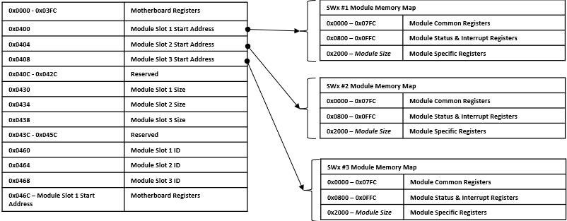
Figure 1. Register Memory Map Addressing for Motherboards with 3 Modules
Address Calculation
Motherboard Registers
Read/Write access to the motherboard registers starts with the base address for the board and then the motherboard base offset address.
For example, to address Module Slot 1 Start Address register (i.e. register address = 0x0400):
- Start with the base address for the board.
- Add the motherboard register address offset.
| Motherboard Address = | Base Address + | Motherboard Address Offset | = 0x0000 0400 |
| 0x0000 0000 | 0x0400 |
Module Registers:
Read/Write access to the Function module’s registers start with the base address of the board. Add the “content” for the Module Start Address and then, add the specific module function register offset.
For example, to address an appropriate/specific function module with a register offset:
- Start with the base address for the board.
- Add the value (contents) from the module base address offset register (contents/value of Motherboard Memory register for Module 1 (i.e., @ 0x0400) = 0x4000.
- Then add the specific module function Register Offset of interest (i.e., A/D Reading Ch 1 @ 0x1000)
| (Function Specific) Address = | Base Address + | Module Base Address Offset + | Function Register Offset | = 0x0000 5000 |
| 0x0000 0000 | 0x4000 | 0x1000 |
REGISTER DESCRIPTIONS
Module Information Registers
The Module Slot Address, Module Slot Size and Module Slot ID provide information about the modules detected on the board.
Link to original
Module Slot Addressing Ready Function: Indicates that the module slots are ready to be addressed. Type: unsigned binary word (32-bit) Data Range: 0x0000 0000 to 0xFFFF FFFF Read/Write: R Initialized Value: 0xA5A5A5A5 Operational Settings: This register will contain the value of 0xA5A5A5A5 when the module addresses have been determined.
Link to original
Module Slot Address Function: Specifies the Base Address for the module in the specific slot position. Type: unsigned binary word (32-bit) Data Range: 0x0000 0000 to 0xFFFF FFFF Read/Write: R Initialized Value: Based on board's module configuration. Operational Settings: 0x0000 0000 indicates no Module found.
Link to original
Module Slot Size Function: Specifies the Memory Size (in bytes) allocated for the module in the specific slot position. Type: unsigned binary word (32-bit) Range: 0x0000 0000 to 0xFFFF FFFF Read/Write: R Initialized Value: Assigned by factory for the module. Operational Settings: 0x0000 0000 indicates no Module found.
Module Slot ID Function: Specifies the Model ID for the module in the specified slot position. Type: 4-character ASCII string Data Range: 0x0000 0000 to 0xFFFF FFFF Read/Write: R Initialized Value: Assigned by factory for the module. Operational Settings: The Module ID is formatted as four ASCII bytes: three characters followed by a space. Module IDs are in little-endian order with a single space following the first three characters. For example, 'TL1' is '1LT', 'SC1' is '1CS' and so forth. Example below is for “TL1” (MSB justified). All value of 0000 0000 indicates no Module found. Link to original
D31 D30 D29 D28 D27 D26 D25 D24 D23 D22 D21 D20 D19 D18 D17 D16 ASCII Character (ex: 'T' - 0x54) ASCII Character (ex: 'L' - 0x4C) D15 D14 D13 D12 D11 D10 D9 D8 D7 D6 D5 D4 D3 D2 D1 D0 ASCII Character (ex: '1' - 0x31) ASCII Space (' ' - 0x20)
Hardware Information Registers
The registers identified in this section provide information about the board’s hardware.
Link to original
Product Serial Number Function: Specifies the Board Serial Number. Type: unsigned binary word (32-bit) Data Range: 0x0000 0000 to 0xFFFF FFFF Read/Write: R Initialized Value: Serial number assigned by factory for the board. Operational Settings: N/A
| Platform | |
| Function: | Specifies the Board Platform Identifier. Values are for the ASCII characters for the NAI valid platforms (Identifiers). |
| Type: | unsigned binary word (32-bit) |
| Data Range: | See table below. |
| Read/Write: | R |
| Initialized Value: | ASCII code is for the Platform Identifier of the board |
| Operational Settings: | Valid NAI platform and the associated value for the platform is shown below: |
| NAI Platform | Platform Identifier | ASCII Binary Values (Note: little-endian order of ascii values) |
| 3U VPX | 68 | 0x0000 3836 |
| Model | |
| Function: | Specifies the Board Model Identifier. Values are for the ASCII characters for the NAI valid models. |
| Type: | unsigned binary word (32-bit) |
| Data Range: | See table below. |
| Read/Write: | R |
| Initialized Value: | ASCII code is for the Model Identifier of the board |
| Operational Settings: | Example of NAI model and the associated value for the model is shown below: |
| NAI Model | ASCII Binary Values (Note: little-endian order of ascii values) |
| SR | 0x0000 5253 |
| Generation | |
| Function: | Specifies the Board Generation Identifier. Values are for the ASCII characters for the NAI valid generation identifiers. |
| Type: | unsigned binary word (32-bit) |
| Data Range: | See table below. |
| Read/Write: | R |
| Initialized Value: | ASCII code is for the Generation Identifier of the board |
| Operational Settings: | Example of NAI generation and the associated value for the generation is shown below: |
| NAI Generation | ASCII Binary Values (Note: little-endian order of ascii values) |
| 1 | 0x0000 0031 |
| Processor Count/Ethernet Interface Count | |
| Function: | Specifies the Processor Count and Ethernet Interface Count |
| Type: | unsigned binary word (32-bit) |
| Data Range: | See table below. |
| Read/Write: | R |
| Operational Settings: | Processor Count - Indicates the number of unique processor types on the motherboard Ethernet Interface Count - Indicates the number of Ethernet interfaces on the product motherboard. For example, Single Ethernet = 1; Dual Ethernet = 2. |
| NAI Board | Processor Count | Description | |
| 3U-VPX | 68SR1 | 1 | Xilinx Zynq 7015 |
| D31 | D30 | D29 | D28 | D27 | D26 | D25 | D24 | D23 | D22 | D21 | D20 | D19 | D18 | D17 | D16 |
| Processor Count (See Table) | |||||||||||||||
| D15 | D14 | D13 | D12 | D11 | D10 | D9 | D8 | D7 | D6 | D5 | D4 | D3 | D2 | D1 | D0 |
| Ethernet Count (Based on Part Number Ethernet Options) | |||||||||||||||
| Maximum Module Slot Count/ARM Platform Type | |
| Function: | Specifies the Maximum Module Slot Count and ARM Platform Type. |
| Type: | unsigned binary word (32-bit) |
| Data Range: | See table below. |
| Read/Write: | R |
| Operational Settings: | Indicates the number of modules that can be installed on the product. ARM Platform Type - Altera = 1; Xilinx X1 = 2; Xilinx X2 = 3; UltraScale = 4 |
| NAI Board | Maximum Module Slot Count | ARM Platform Type | |
| 3U-VPX | 68SR1 | 3 | Xilinx X2 = 3 |
| D31 | D30 | D29 | D28 | D27 | D26 | D25 | D24 | D23 | D22 | D21 | D20 | D19 | D18 | D17 | D16 |
| Maximum Module Slot Count (See Table) | |||||||||||||||
| D15 | D14 | D13 | D12 | D11 | D10 | D9 | D8 | D7 | D6 | D5 | D4 | D3 | D2 | D1 | D0 |
| ARM Platform Type (See Table) | |||||||||||||||
Motherboard Firmware Information Registers
The registers in this section provide information on the revision of the firmware installed on the motherboard.
Motherboard Core (MBCore) Firmware Version Function: Specifies the Version of the NAI factory provided Motherboard Core Application installed on the board. Type: Two (2) unsigned binary word (32-bit) Data Range: 0x0000 0000 to 0xFFFF FFFF Read/Write: R Operational Settings: The motherboard firmware version consists of four components: Major, Minor, Minor 2 and Minor 3. Link to original
Motherboard Core Firmware Version (Note: little-endian order in register) (ex. 4.7.0.0) Word 1 (Ex. 0007 0004 = 4.7 (Major.Minor) D31 D30 D29 D28 D27 D26 D25 D24 D23 D22 D21 D20 D19 D18 D17 D16 Minor (ex: 0x0007 = 7) D15 D14 D13 D12 D11 D10 D9 D8 D7 D6 D5 D4 D3 D2 D1 D0 Major (ex: 0x0004 = 4) Word 2 (Ex. 0x0000 0000 = 0000 = 0.0 (Minor2.Minor3)) D31 D30 D29 D28 D27 D26 D25 D24 D23 D22 D21 D20 D19 D18 D17 D16 Minor 3 (ex: 0x000 = 0) D15 D14 D13 D12 D11 D10 D9 D8 D7 D6 D5 D4 D3 D2 D1 D0 Minor 2 (ex: 0x000 = 0)
Motherboard Firmware Build Time/Date Function: Specifies the Build Date/Time of the NAI factory provided Motherboard Core Application installed on the board. Type: Two (2) unsigned binary word (32-bit) Data Range: N/A Read/Write: R Operational Settings: The motherboard firmware time consists of the Build Date and Build Time. NOTE: On some builds the the Date/Time fields are fixed to 0000 0000 to maintain binary consistency across builds. Link to original
Motherboard Firmware Build Time (Note: little-endian order in register) Word 1 - Build Date (ex. 0x030C 07E2 = 2018-12-03) D31 D30 D29 D28 D27 D26 D25 D24 D23 D22 D21 D20 D19 D18 D17 D16 Day (ex: 0x03 = 3) Month (ex: 0x0C = 12) D15 D14 D13 D12 D11 D10 D9 D8 D7 D6 D5 D4 D3 D2 D1 D0 Year (ex: 0x07E2 = 2018) Word 2 - Build Time (ex. 0x001B 3B0A = 10:59:27) D31 D30 D29 D28 D27 D26 D25 D24 D23 D22 D21 D20 D19 D18 D17 D16 null (0x00) Seconds (ex: 0x1B = 27) D15 D14 D13 D12 D11 D10 D9 D8 D7 D6 D5 D4 D3 D2 D1 D0 Minutes (ex: 0x3B = 59) Hours (ex: 0x0A = 10)
Motherboard FPGA Revision Function: Specifies the Version of the NAI factory provided Motherboard FPGA installed on the board. Type: unsigned binary word (32-bit) Data Range: 0x0000 0000 to 0xFFFF FFFF Read/Write: R Operational Settings: The motherboard FPGA firmware version consists of two components: Major, Minor. Link to original
Motherboard FPGA Firmware Version (ex. 0x0005 0008 = 5.8) D31 D30 D29 D28 D27 D26 D25 D24 D23 D22 D21 D20 D19 D18 D17 D16 Major (ex: 0x0005 = 5) D15 D14 D13 D12 D11 D10 D9 D8 D7 D6 D5 D4 D3 D2 D1 D0 Minor (ex: 0x0008 = 8)
Motherboard FPGA Compile Date/Time Function: Specifies the Compile Date/Time of the NAI factory provided Motherboard FPGA installed on the board. Type: unsigned binary word (32-bit) Data Range: N/A Read/Write: R Operational Settings: The motherboard firmware time consists of the Build Date and Time in the following format: Link to original
Motherboard FPGA Compile Time (ex. 0xD12A 01B8 = 02/26/21 00:06:56) D31 D30 D29 D28 D27 D26 D25 D24 D23 D22 D21 D20 D19 D18 D17 D16 Day (D31:D27) Month (D26:D23) Year (D22:D17) ex. 0xD ex. 0x1 0x2 0xA 1 1 0 1 0 0 1 0 0 0 1 0 1 0 1 1 Day = 0x1A = 26 Month = 0x2 = 2 Year = 0x15 = 21 D15 D14 D13 D12 D11 D10 D9 D8 D7 D6 D5 D4 D3 D2 D1 D0 Hour (D16:D12) Minutes (D11:D6) Seconds (D5:D0) ex. 0x0 ex. 0x1 ex. 0xB ex. 0x8 Hour = 0x00 = 0 Minutes = 0x06 = 06 Seconds = 0x38 = 56
Motherboard Monitoring Registers
The registers in this provide motherboard temperature measurement information.
Temperature Readings Register
The temperature registers provide the current, maximum (from power-up) and minimum (from power-up) for the processor and PCB for Zynq processor.
These registers are only available on Xilinx Generation 5 platforms, and are periodically populated by the motherboard core application, which only runs in Petalinux and BareMetal. For other operating systems, refer to the naibrd Software Support Kit (SSK) naibsp_system_Monitor_Temperature_Get() routine to manually retrieve the temperature (NOTE: this feature is typically utilized for development/factory use only; contact the factory for additional details on potential use, if required).
Temperature Readings Register Function: Specifies the Measured Temperatures on Motherboard. Type: signed byte (8-bits) for each temperature reading - Six (6) 32-bit words Data Range: 0x0000 0000 to 0xFFFF 0000 Read/Write: R Initialized Value: Value corresponding to the measured temperatures based on the table below. Operational Settings: The 8-bit temperature readings are signed bytes. For example, if the following register contains the value 0x6955 0000:
Word 3 (Max Zynq Temperatures) D31 D30 D29 D28 D27 D26 D25 D24 D23 D22 D21 D20 D19 D18 D17 D16 Max Zynq Core Temperature Max Zynq PCB Temperature D15 D14 D13 D12 D11 D10 D9 D8 D7 D6 D5 D4 D3 D2 D1 D0 0x00 0x00 The values would represent the following temperatures:
Temperature Measurements Data Bits Value Temperature (Celsius) Max Zynq Core Temperature D31:D24 0x69 +105° Max Zynq PCB Temperature D23:D16 0x55 +85° Link to original
Temperature Readings Word 1 (Current Zynq Temperatures) D31 D30 D29 D28 D27 D26 D25 D24 D23 D22 D21 D20 D19 D18 D17 D16 Zynq Core Temperature Zynq PCB Temperature D15 D14 D13 D12 D11 D10 D9 D8 D7 D6 D5 D4 D3 D2 D1 D0 0x00 0x00 Word 2 (Reserved) D31 D30 D29 D28 D27 D26 D25 D24 D23 D22 D21 D20 D19 D18 D17 D16 0x00 0x00 D15 D14 D13 D12 D11 D10 D9 D8 D7 D6 D5 D4 D3 D2 D1 D0 0x00 0x00 Word 3 (Max Zynq Temperatures) D31 D30 D29 D28 D27 D26 D25 D24 D23 D22 D21 D20 D19 D18 D17 D16 Max Zynq Core Temp Max Zynq PCB Temp D15 D14 D13 D12 D11 D10 D9 D8 D7 D6 D5 D4 D3 D2 D1 D0 0x00 0x00 Word 4 (Reserved) D31 D30 D29 D28 D27 D26 D25 D24 D23 D22 D21 D20 D19 D18 D17 D16 0x00 0x00 D15 D14 D13 D12 D11 D10 D9 D8 D7 D6 D5 D4 D3 D2 D1 D0 0 0 0 0 0 0 0 0 0 0 0 0 0 0 0 0 Word 5 (Min Zynq Temperatures) D31 D30 D29 D28 D27 D26 D25 D24 D23 D22 D21 D20 D19 D18 D17 D16 Min Zynq Core Temperature Min Zynq PCB Temperature D15 D14 D13 D12 D11 D10 D9 D8 D7 D6 D5 D4 D3 D2 D1 D0 0 0 0 0 0 0 0 0 0 0 0 0 0 0 0 0 Word 6 (Reserved) D31 D30 D29 D28 D27 D26 D25 D24 D23 D22 D21 D20 D19 D18 D17 D16 0x00 0x00 D15 D14 D13 D12 D11 D10 D9 D8 D7 D6 D5 D4 D3 D2 D1 D0 0 0 0 0 0 0 0 0 0 0 0 0 0 0 0 0
Higher Precision Temperature Readings Register
These registers provide higher precision readings of the current Zynq and PCB temperatures.
Higher Precision Zynq Core Temperature Function: Specifies the Higher Precision Measured Zynq Core temperature on Interface Board. Type: signed word (16-bits) for integer part and unsigned word (16-bits) for fractional part Data Range: 0x0000 0000 to 0xFFFF FFFF Read/Write: R Initialized Value: Measured Zynq Core temperature on Interface Board Operational Settings: The upper 16-bits represent the signed integer part of the temperature and the lower 16-bits represent the fractional part of the temperature with the resolution of 1/1000 of degree Celsius. For example, if the register contains the value 0x002B 0271, this represents Zynq Core Temperature = 43.625° Celsius, and value 0xFFF6 0177 represents -10.375° Celsius. Link to original
D31 D30 D29 D28 D27 D26 D25 D24 D23 D22 D21 D20 D19 D18 D17 D16 Signed Integer Part of Temperature D15 D14 D13 D12 D11 D10 D9 D8 D7 D6 D5 D4 D3 D2 D1 D0 Fractional Part of Temperature
Higher Precision Motherboard PCB Temperature Function: Specifies the Higher Precision Measured Motherboard PCB temperature. Type: signed word (16-bits) for integer part and unsigned word (16-bits) for fractional part Data Range: 0x0000 0000 to 0xFFFF FFFF Read/Write: R Initialized Value: Measured Motherboard PCB temperature Operational Settings: The upper 16-bits represent the signed integer part of the temperature and the lower 16-bits represent the fractional part of the temperature with the resolution of 1/1000 of degree Celsius. For example, if the register contains the value 0x0020 007D, this represents Interface PCB Temperature = 32.125° Celsius, and value 0xFFE8 036B represents -24.875° Celsius. Link to original
D31 D30 D29 D28 D27 D26 D25 D24 D23 D22 D21 D20 D19 D18 D17 D16 Signed Integer Part of Temperature D15 D14 D13 D12 D11 D10 D9 D8 D7 D6 D5 D4 D3 D2 D1 D0 Fractional Part of Temperature
Motherboard Health Monitoring Registers
The registers in this section provide a summary of motherboard temperature sensors and their corresponding bits. Additionally, this section provides an overview of the registers allocated to those sensors, which are used to monitor current/minimum/maximum temperature readings, upper & lower critical/warning temperature thresholds, and whether or not a programmed temperature threshold has been exceeded.
These registers are only available on Xilinx Generation 5 platforms, and are periodically populated by the motherboard core application, which only runs in Petalinux and BareMetal. For other operating systems, refer to the naibrd Software Support Kit (SSK) naibsp_system_Monitor_Temperature_Get() routine to manually retrieve the temperature (NOTE: this feature is typically utilized for development/factory use only; contact the factory for additional details on potential use, if required).
Motherboard Sensor Summary Alarm Function: The corresponding sensor bit is set if the sensor has crossed any of its thresholds. Type: unsigned binary word (32-bits) Data Range: See table below Read/Write: R Initialized Value: 0 Operational Settings: This register provides a summary for motherboard sensors. When the corresponding sensor bit is set, the Sensor Threshold Status register for that sensor will indicate the threshold condition that triggered the event. Link to original
Bit(s) Sensor D31:D5 Reserved D4 Motherboard PCB Temperature D3 Zynq Core Temperature D2:D0 Reserved
Motherboard Sensor Registers
The registers listed in this section apply to each module sensor listed for the Motherboard Sensor Summary Status register. Each individual sensor register provides a group of registers for monitoring motherboard temperatures readings. From these registers, a user can read the current temperature of the sensor in addition to the minimum and maximum temperature readings since power-up. Upper and lower critical/warning temperature thresholds can be set and monitored from these registers. When a programmed temperature threshold is crossed, the Sensor Threshold Status register will set the corresponding bit for that threshold. The figure below shows the functionality of this group of registers when accessing the Zynq Core Temperature sensor as an example.
Link to original

Sensor Threshold Status Function: Reflects which threshold has been crossed Type: unsigned binary word (32-bits) Data Range: See table below Read/Write: R Initialized Value: 0 Operational Settings: The associated bit is set when the sensor reading exceed the corresponding threshold settings. Link to original
Bit(s) Description D31:D4 Reserved D3 Exceeded Upper Critical Threshold D2 Exceeded Upper Warning Threshold D1 Exceeded Lower Critical Threshold D0 Exceeded Lower Warning Threshold
Link to original
Sensor Current Reading Function: Reflects current reading of temperature sensor Type: Single Precision Floating Point Value (IEEE-754) Data Range: Single Precision Floating Point Value (IEEE-754) Read/Write: R Initialized Value: N/A Operational Settings: The register represents current sensor reading as a single precision floating point value. For example, for a temperature sensor, register value 0x41C6 0000 represents temperature = 24.75° Celsius.
Link to original
Sensor Minimum Reading Function: Reflects minimum value of temperature sensor since power up Type: Single Precision Floating Point Value (IEEE-754) Data Range: Single Precision Floating Point Value (IEEE-754) Read/Write: R Initialized Value: N/A Operational Settings: The register represents minimum sensor value as a single precision floating point value. For example, for a temperature sensor, register value 0x41C6 0000 represents temperature = 24.75° Celsius.
Link to original
Sensor Maximum Reading Function: Reflects maximum value of temperature sensor since power up Type: Single Precision Floating Point Value (IEEE-754) Data Range: Single Precision Floating Point Value (IEEE-754) Read/Write: R Initialized Value: N/A Operational Settings: The register represents maximum sensor value as a single precision floating point value. For example, for a temperature sensor, register value 0x41C6 0000 represents temperature = 24.75° Celsius.
Link to original
Sensor Lower Warning Threshold Function: Reflects lower warning threshold of temperature sensor Type: Single Precision Floating Point Value (IEEE-754) Data Range: Single Precision Floating Point Value (IEEE-754) Read/Write: R/W Initialized Value: Default lower warning threshold (value dependent on specific sensor) Operational Settings: The register represents sensor lower warning threshold as a single precision floating point value. For example, for a temperature sensor, register value 0xC220 0000 represents temperature = -40.0° Celsius.
Link to original
Sensor Lower Critical Threshold Function: Reflects lower critical threshold of temperature sensor Type: Single Precision Floating Point Value (IEEE-754) Data Range: Single Precision Floating Point Value (IEEE-754) Read/Write: R/W Initialized Value: Default lower critical threshold (value dependent on specific sensor) Operational Settings: The register represents sensor lower critical threshold as a single precision floating point value. For example, for a temperature sensor, register value 0xC25C 0000 represents temperature = -55.0° Celsius.
Link to original
Sensor Upper Warning Threshold Function: Reflects upper warning threshold of temperature sensor Type: Single Precision Floating Point Value (IEEE-754) Data Range: Single Precision Floating Point Value (IEEE-754) Read/Write: R/W Initialized Value: Default upper warning threshold (value dependent on specific sensor) Operational Settings: The register represents sensor upper warning threshold as a single precision floating point value. For example, for a temperature sensor, register value 0x42AA 0000 represents temperature = 85.0° Celsius.
Link to original
Sensor Upper Critical Threshold Function: Reflects upper critical threshold of temperature sensor Type: Single Precision Floating Point Value (IEEE-754) Data Range: Single Precision Floating Point Value (IEEE-754) Read/Write: R/W Initialized Value: Default upper critical threshold (value dependent on specific sensor) Operational Settings: The register represents sensor upper critical threshold as a single precision floating point value. For example, for a temperature sensor, register value 0x42FA 0000 represents temperature = 125.0° Celsius.
Ethernet Configuration Registers
The registers in this section provide information about the Ethernet Configuration for the two ports on the board.
Important: Regardless if the board is configured for one or two Ethernet ports, the second IP address cannot be on the same Subnet as the First IP Address. The table below provides examples of valid and invalid IP Addresses and Subnet Mask Addresses.
Link to original
First Port (A) IP Address First Port (A) Subnet Mask Second Port (B) IP Address Second Port (B) Subnet Mask Result 192.168.1.5 255.255.255.0 192.168.2.5 255.255.255.0 Good 192.168.1.5 255.255.0.0 192.168.2.5 255.255.0.0 Conflict 192.168.1.5 255.255.0.0 192.168.2.5 255.255.255.0 Conflict 10.0.0.15 255.0.0.0 192.168.1.5 255.255.255.0 Good
Ethernet MAC Address and Ethernet Settings Function: Specifies the Ethernet MAC Address and Ethernet Settings for the Ethernet port. Type: Two (2) unsigned binary word (32-bit) Data Range: See table. Read/Write: R Operational Settings: The Ethernet MAC Address consists of six octets. The Ethernet Settings are defined in table.
Bits Description Values D31:D23 Reserved 0 D22:D21 Duplex 00 = Not Specified
01 = Half Duplex
10 = Full Duplex
11 = ReservedD20:D18 Speed 000 = Not Specified
001 = 10 Mbps
010 = 100 Mbps
011 = 1000 Mbps
100 = 2500 Mbps
101 = 10000 Mbps
110 = Reserved
111 = ReservedD17 Auto Negotiate 0 = Enabled
1 = DisabledD16 Static IP Address 0 = Enabled
1 = DisabledLink to original
Ethernet MAC Address and Ethernet Settings (Note: little-endian order in register) Word 1 (Ethernet MAC Address (Octets 1-4)) (ex: aa:bb:cc:dd:ee:ff) D31 D30 D29 D28 D27 D26 D25 D24 D23 D22 D21 D20 D19 D18 D17 D16 MAC Address Octet 4 (ex: 0xDD) MAC Address Octet 3 (ex: 0xCC) D15 D14 D13 D12 D11 D10 D9 D8 D7 D6 D5 D4 D3 D2 D1 D0 MAC Address Octet 2 (ex: 0xBB) MAC Address Octet 1 (ex: 0xAA) Word 2 (Ethernet MAC Address (Octets 5-6) and Ethernet Settings) D31 D30 D29 D28 D27 D26 D25 D24 D23 D22 D21 D20 D19 D18 D17 D16 Ethernet Settings (See table) D15 D14 D13 D12 D11 D10 D9 D8 D7 D6 D5 D4 D3 D2 D1 D0 MAC Address Octet 6 (ex: 0xFF) MAC Address Octet 5 (ex: 0xEE)
Ethernet Interface Name Function: Specifies the Ethernet Interface Name for the Ethernet port. Type: 8-character ASCII string Data Range: See table. Read/Write: R Operational Settings: The Ethernet Interface Name (eth0, eth1, etc) for the Ethernet port. Link to original
Ethernet Interface Name (Note: ascii string in register) (ex. “eth0”) Word 1 (Bit 0-31) (ex: 0x3068 7465 = “0hte”) D31 D30 D29 D28 D27 D26 D25 D24 D23 D22 D21 D20 D19 D18 D17 D16 ASCII Character (ex: '0' - 0x30) ASCII Character (ex: 'h' - 0x68) D15 D14 D13 D12 D11 D10 D9 D8 D7 D6 D5 D4 D3 D2 D1 D0 ASCII Character (ex: 't' - 0x74) ASCII Character (ex: 'e' - 0x65) Word 2 (Bit 32-63) (ex: 0x0000 0000) D31 D30 D29 D28 D27 D26 D25 D24 D23 D22 D21 D20 D19 D18 D17 D16 ASCII Character (ex: null - 0x00) ASCII Character (ex: null - 0x00) D15 D14 D13 D12 D11 D10 D9 D8 D7 D6 D5 D4 D3 D2 D1 D0 ASCII Character (ex: null - 0x00) ASCII Character (ex: null - 0x00)
Ethernet IPv4 Address Function: Specifies the Ethernet IPv4 Address for the Ethernet port. Type: Three (3) unsigned binary word (32-bit) Data Range: See table. Read/Write: R Operational Settings: The Ethernet IPv4 Address consists of three parts: IPv4 Address, IPv4 Subnet Mask and IPv4 Gateway. Link to original
Ethernet IPv4 Address (Note: little-endian order in register) Word 1 (Ethernet IPv4 Address) (ex: 0x1001 A8C0 = 192.168.1.16) D31 D30 D29 D28 D27 D26 D25 D24 D23 D22 D21 D20 D19 D18 D17 D16 IPv4 Address Octet 4 (ex: 0x10 = 16) IPv4 Address Octet 3 (ex: 0x01 = 1) D15 D14 D13 D12 D11 D10 D9 D8 D7 D6 D5 D4 D3 D2 D1 D0 IPv4 Address Octet 2 (ex: 0xA8 = 168) IPv4 Address Octet 1 (ex: 0xC0 = 192) Word 2 (Ethernet IPv4 Subnet) (ex: 0x00FF FFFF = 255.255.255.0) D31 D30 D29 D28 D27 D26 D25 D24 D23 D22 D21 D20 D19 D18 D17 D16 IPv4 Subnet Octet 4 (ex: 0x00 = 0) IPv4 Subnet Octet 3 (ex: 0xFF = 255) D15 D14 D13 D12 D11 D10 D9 D8 D7 D6 D5 D4 D3 D2 D1 D0 IPv4 Subnet Octet 2 (ex: 0xFF = 255) IPv4 Subnet Octet 1 (ex: 0xFF = 255) Word 3 (Ethernet IPv4 Gateway) (ex: 0x0101 A8C0 = 192.168.1.1) D31 D30 D29 D28 D27 D26 D25 D24 D23 D22 D21 D20 D19 D18 D17 D16 IPv4 Gateway Octet 4 (ex: 0x01 = 1) IPv4 Gateway Octet 3 (ex: 0x01 = 1) D15 D14 D13 D12 D11 D10 D9 D8 D7 D6 D5 D4 D3 D2 D1 D0 IPv4 Gateway Octet 2 (ex: 0xA8 = 168) IPv4 Gateway Octet 1 (ex: 0xC0 = 192)
Ethernet IPv6 Address Function: Specifies the Ethernet IPv6 Address for the Ethernet port. Type: Five (5) unsigned binary word (32-bit) Data Range: See table. Read/Write: R Operational Settings: The IPv6 Prefix length indicates the network portion of an IPv6 address using the following format: IPv6 address/prefix length ` Prefix length can range from 0 to 128 ` * Typical prefix length is 64 The following is an illustration of IPv6 addressing with IPv6 Prefix length of 64.
64 bits 64 bits Prefix Interface ID Prefix 1 Prefix 2 Prefix 3 Subnet ID Interface ID 1 Interface ID 2 Interface ID 3 Interface ID 4 Example: 2002:c0a8:101:0:7c99:d118:9058:1235/64 2002 C0A8 0101 0000 7C99 D118 9058 1235 Link to original
Ethernet IPv6 Address (Note: little-endian order within 32-bit and 16-bit words in register) (ex. IPv6 Address: 2002:c0a8:201:0:7c99:d118:9058:1235 IPv6 Prefix: 64) Word 1 (Ethernet IPv6 Address (Prefix 1-2)) (ex:0xA8C0 0220 = 2002 C0A8) D31 D30 D29 D28 D27 D26 D25 D24 D23 D22 D21 D20 D19 D18 D17 D16 Prefix 2 (ex: 0xA8C0 = C0A8) D15 D14 D13 D12 D11 D10 D9 D8 D7 D6 D5 D4 D3 D2 D1 D0 Prefix 1 (ex: 0x0220 = 2002) Word 2 (Ethernet IPv6 Address (Prefix 3/Subnet ID)) + (ex:0x000 0101 = 0101 0000) D31 D30 D29 D28 D27 D26 D25 D24 D23 D22 D21 D20 D19 D18 D17 D16 Subnet ID (ex: 0x0000 = 0000) D15 D14 D13 D12 D11 D10 D9 D8 D7 D6 D5 D4 D3 D2 D1 D0 Prefix 3 (ex: 0x0101 = 0101) Word 3 (Ethernet IPv6 Address (Interface ID 1-2)) + (ex: 0x18D1 997C = 7C99 D118) D31 D30 D29 D28 D27 D26 D25 D24 D23 D22 D21 D20 D19 D18 D17 D16 Interface ID 2 (ex: 0x18D1 = D118) D15 D14 D13 D12 D11 D10 D9 D8 D7 D6 D5 D4 D3 D2 D1 D0 Interface ID 1 (ex: 0x997C = 7C99) Word 4 (Ethernet IPv6 Address (Interface ID 3-4)) + (ex: 0x3512 5890 = 9058 1235) D31 D30 D29 D28 D27 D26 D25 D24 D23 D22 D21 D20 D19 D18 D17 D16 Interface ID 4 (ex: 0x3512 = 1235) D15 D14 D13 D12 D11 D10 D9 D8 D7 D6 D5 D4 D3 D2 D1 D0 Interface ID 3 (ex: 0x5890 = 9058) Word 5 (Ethernet IPv6 Prefix Length) + (ex:0x0000 0040) D31 D30 D29 D28 D27 D26 D25 D24 D23 D22 D21 D20 D19 D18 D17 D16 0 0 0 0 0 0 0 0 0 0 0 0 0 0 0 0 D15 D14 D13 D12 D11 D10 D9 D8 D7 D6 D5 D4 D3 D2 D1 D0 Prefix Length (ex: 0x0040 = 64)
Interrupt Vector and Steering
When interrupts are enabled, the interrupt vector associated with the specific interrupt can be programmed (typically with a unique number/identifier) such that it can be utilized in the Interrupt Service Routine (ISR) to identify the type of interrupt. When an interrupt occurs, the contents of the Interrupt Vector registers is reported as part of the interrupt mechanism. In addition to specifying the interrupt vector, the interrupt can be directed (“steered”) to the native bus or to the application running on the onboard ARM processor.
Note
The Interrupt Vector and Interrupt Steering registers are mapped to the Motherboard Common Memory and these registers are associated with the Module Slot position (refer to Function Register Map).
Interrupt Vector Function: Set an identifier for the interrupt. Type: unsigned binary word (32-bit) Data Range: 0x0000 0000 to 0xFFFF FFFF Read/Write: R/W Initialized Value: 0 Operational Settings: When an interrupt occurs, this value is reported as part of the interrupt mechanism.
Interrupt Steering Function: Sets where to direct the interrupt. Type: unsigned binary word (32-bit) Data Range: See table Read/Write: R/W Initialized Value: 0 Operational Settings: When an interrupt occurs, the interrupt is sent as specified: Link to original
Direct Interrupt to VME 1 Direct Interrupt to ARM Processor (via SerDes)
(Custom App on ARM or NAI Ethernet Listener App)2 Direct Interrupt to PCIe Bus 5 Direct Interrupt to cPCI Bus 6
Module Control Command Registers
Modules Control Command Requests Function: Provides the ability to command individual Modules to Reset, Power-down, or Power-up. Type: unsigned binary word (32-bit) Data Range: 0x0000 0000 to 0xFFFF FFFF Read/Write: R/W Operational Settings: The Module Control Commands registers provide the ability to request individual Modules to perform one of the following functions - Reset, Power-down, Power-up. Only one command can be requested at a time per Module. For example, one can't request a Reset and a Power-down at the same time for the same Module. Once the command is recognized and handled, the bit will be cleared. Note
Clearing of the command request bit only indicates the command has been recognized and initiated, it does not indicate that the command action has been completed.
There is one Control Command Request register per Module. Each register is Bit-mapped as shown in the table below:
Link to original
Bit(s) Description D31:D3 Reserved D2 Module Power-up D1 Module Power-down D0 Module Reset
Modules Health Monitoring Registers
Module Communications Status Function: Provides the ability to monitor factors may effect communication status of a Module. Type: unsigned binary word (32-bit) Data Range: 0x0000 0000 to 0xFFFF FFFF Read/Write: R Operational Settings: The Module Communications registers provide the ability to monitor factors that may effect the Communications Status of individual Modules. There is one register per Module. Each communication factor is bit mapped to the register as shown in the table below:
Bit(s) Description D31:D5 Reserved D4 Module Communications Error Detected D3 Module Firmware Not Ready D2 Module LinkInit Not Done D1 Module Not Detected D0 Module Powered-down Module Powered-down: The user can request an individual Module be powered-down (see Module Control Command Requests). Once the request is detected and acted upon, this bit will be set. Once powered-down, you will not be able to communicate with the Module.
Module Not Detected: If a Module in this slot has not been detected, you will not be able to communicate with the Module.
Module LinkInit Not Done: Module communications is accomplished via SERDES. LinkInit is required to establish a connection to the Module. If the LinkInit has not been successfully completed, you will not be able to communicate with the Module.
Module Firmware Not Ready: Each Module has Firmware that is ready from Module QSPI and loaded for execution. If this Firmware was not loaded and started successfully, you may not be able to communicate with the Module.
Module Communications Error Detected: If at some point during run-time, communications with the Module has failed, this bit will be set.
Link to original
Module BIT Status Function: Provides the ability to monitor the individual Module BIT Status. Type: unsigned binary word (32-bit) Data Range: 0x0000 0000 to 0xFFFF FFFF Read/Write: R Operational Settings: The Module BIT Status registers provide the ability to monitor individual Module BIT results as Latched and current value. A 1 is any bit field indicates BIT failure for the Module in that slot. Link to original
Bit(s) Description D31:D20 Reserved D19 Module Slot 3 BIT Failure (current value) D18 Module Slot 2 BIT Failure (current value) D17 Module Slot 1 BIT Failure (current value) D16 Reserved D15:D4 Reserved D3 Module Slot 3 BIT Failure - Latched D2 Module Slot 2 BIT Failure - Latched D1 Module Slot 1 BIT Failure - Latched D0 Reserved
Scratchpad Area
Link to original
Scratchpad Area Function: Registers reserved as scratch pad for customer use. Type: unsigned binary word (32-bit) Data Range: 0x0000 0000 to 0xFFFF FFFF Read/Write: R/W Operational Settings: This area in memory is reserved for customer use.
MOTHERBOARD FUNCTION REGISTER MAP
Key:
| Configuration/Control |
| Measurement/Status/Board Information |
| MODULE INFORMATION REGISTERS | |||||
| OFFSET | REGISTER NAME | ACCESS | OFFSET | REGISTER NAME | ACCESS |
| 0x03FC | Module Slot Addressing Ready | R | |||
| 0x0400 | Module Slot 1 Address | R | 0x0430 | Module Slot 1 Size | R |
| 0x0404 | Module Slot 2 Address | R | 0x0434 | Module Slot 2 Size | R |
| 0x0408 | Module Slot 3 Address | R | 0x0438 | Module Slot 3 Size | R |
| 0x0460 | Module Slot 1 ID | R | |||
| 0x0464 | Module Slot 2 ID | R | |||
| 0x0468 | Module Slot 3 ID | R | |||
| HARDWARE INFORMATION REGISTERS | |||||
| OFFSET | REGISTER NAME | ACCESS | OFFSET | REGISTER NAME | ACCESS |
| 0x0020 | Product Serial Number | R | |||
| 0x0024 | Platform | R | 0x0030 | Processor Count/Ethernet Count | R |
| 0x0028 | Model | R | 0x0034 | Maximum Module Slot Count/ARM Platform Type | R |
| 0x002C | Generation | R | |||
| MOTHERBOARD FIRMWARE INFORMATION REGISTERS | |||||
| OFFSET | REGISTER NAME | ACCESS | OFFSET | REGISTER NAME | ACCESS |
| Motherboard Core Information | Motherboard FPGA Information | ||||
| 0x0100 | MB Core Major/Minor Version | R | 0x0270 | MB FPGA Revision | R |
| 0x0104 | MB Core Minor 2/3 Version | R | 0x0274 | MB FPGA Compile Date/Time | R |
| 0x0108 | MB Core Build Date | R | |||
| MOTHERBOARD MONITORING REGISTERS | |||||
| OFFSET | REGISTER NAME | ACCESS | OFFSET | REGISTER NAME | ACCESS |
| Temperature Readings | High Precision Temperature Readings | ||||
| 0x0200 | Current Zynq Temperatures | R | 0x0230 | Current Zynq Core Temperature | R |
| 0x0204 | Reserved | R | 0x0234 | Current Zynq PCB Temperature | R |
| 0x0208 | Max Zynq Temp | R | |||
| 0x020C | Reserved | R | |||
| 0x0210 | Min Zynq Temperatures | R | |||
| 0x0214 | Reserved | R | |||
| MOTHERBOARD HEALTH MONITORING REGISTERS | |||||
| OFFSET | REGISTER NAME | ACCESS | OFFSET | REGISTER NAME | ACCESS |
| 0x20F8 | Motherboard Sensor Summary Status | R | |||

| ETHERNET CONFIGURATION REGISTERS | |||||
| OFFSET | REGISTER NAME | ACCESS | OFFSET | REGISTER NAME | ACCESS |
| ETHERNET A (LEFT) / ETHERNET B (RIGHT) | |||||
| 0x0070 | Ethernet A MAC (Octets 1-4) | R | 0x00A0 | Ethernet B MAC (Octets 1-4) | R |
| 0x0074 | Ethernet A MAC (Octets 5-6)/Misc Settings | R | 0x00A4 | Ethernet B MAC (Octets 5-6)/Misc Settings | R |
| 0x0078 | Ethernet A Interface Name (Bit 0-31) | R | 0x00A8 | Ethernet B Interface Name (Bit 0-31) | R |
| 0x007C | Ethernet A Interface Name (Bit 32-63) | R | 0x00AC | Ethernet B Interface Name (Bit 32-63) | R |
| 0x0080 | Ethernet A IPv4 Address | R | 0x00B0 | Ethernet B IPv4 Address | R |
| 0x0084 | Ethernet A IPv4 Subnet Mask | R | 0x00B4 | Ethernet B IPv4 Subnet Mask | R |
| 0x0088 | Ethernet A IPv4 Gateway | R | 0x00B8 | Ethernet B IPv4 Gateway | R |
| 0x008C | Ethernet A IPv6 Address (Prefix 1-2) | R | 0x00BC | Ethernet B IPv6 Address (Prefix 1-2) | R |
| 0x0090 | Ethernet A IPv6 Address (Prefix 3/Subnet ID) | R | 0x00C0 | Ethernet B IPv6 Address (Prefix 3/Subnet ID) | R |
| 0x0094 | Ethernet A IPv6 Address (Interface ID 1-2) | R | 0x00C4 | Ethernet B IPv6 Address (Interface ID 1-2) | R |
| 0x0098 | Ethernet A IPv6 Address (Interface ID 3-4) | R | 0x00C8 | Ethernet B IPv6 Address (Interface ID 3-4) | R |
| 0x009C | Ethernet A IPv6 Prefix Length | R | 0x00CC | Ethernet B IPv6 Prefix Length | R |
| INTERRUPT REGISTERS | |||||
| OFFSET | REGISTER NAME | ACCESS | OFFSET | REGISTER NAME | ACCESS |
| 0x0500 - 0x057C | Module 1 Interrupt Vector 1 - 32 | R/W | 0x0600 - 0x067C | Module 1 Interrupt Steering 1 - 32 | R/W |
| 0x0700 - 0x077C | Module 2 Interrupt Vector 1 - 32 | R/W | 0x0800 - 0x087C | Module 2 Interrupt Steering 1 - 32 | R/W |
| 0x0900 - 0x097C | Module 3 Interrupt Vector 1 - 32 | R/W | 0x0A00 - 0x0A7C | Module 3 Interrupt Steering 1 - 32 | R/W |
| MODULE CONTROL COMMAND REQUEST REGISTERS | |||||
| OFFSET | REGISTER NAME | ACCESS | OFFSET | REGISTER NAME | ACCESS |
| 0x01D8 | Module Slot 1 Command Request | R/W | |||
| 0x01DC | Module Slot 2 Command Request | R/W | |||
| 0x01E0 | Module Slot 3 Command Request | R/W | |||
| MODULES HEALTH MONITORING REGISTERS | |||||
| OFFSET | REGISTER NAME | ACCESS | OFFSET | REGISTER NAME | ACCESS |
| 0x01B8 | Module Slot 1 Communications Status | R | 0x0128 | Module BIT Status (current and latched) | R |
| 0x01BC | Module Slot 2 Communications Status | R | |||
| 0x01C0 | Module Slot 3 Communications Status | R | |||
| SCRATCHPAD REGISTERS | |||||
| OFFSET | REGISTER NAME | ACCESS | OFFSET | REGISTER NAME | ACCESS |
| 0x3800 - 0x3BFF | Scratchpad Registers | R/W | |||
ETHERNET
(For detailed supplement, please visit the NAI web-site specific product page and refer to: Ethernet Interface for Generation 5 SBC and Embedded IO Boards Specification)
Note
For products capable of 10/100/1000Base-KX functionality - the product Ethernet PHY supports 1000BASE-X. Product interoperability with 10/100/1000BASE-KX is supported with 1000BASE-X (provided that auto-negotiation is disabled).
The Ethernet Interface Option allows communications and control access to all function modules either via the system BUS or Ethernet ports 1 or 2.
Ethernet 1 Ethernet 2 Ethernet 3* Ethernet 4* (REF PORT A) (REF PORT B) (REF PORT C) (REF PORT D) The default IP address: 192.168.1.16 192.168.2.16 192.168.3.16 192.168.4.16 The default subnet: 255.255.255.0 255.255.255.0 255.255.255.0 255.255.255.0 The default gateway: 192.168.1.1 192.168.2.1 192.168.3.1 192.168.4.1 *see Part Number Designation for applicability.
Note
Actual “as shipped” card Ethernet default IP addresses may vary based upon final ATP configuration(s).
The NAI interface supports IPv4 and IPv6 and both the TCP and UDP protocols. The Ethernet Operation Mode Command Listener application running on the motherboard host processor implements the operation interface. The listener is operational on startup through the nai_MBStartup process and listen on specific ports for commands to process. The default ports are listed below:
- TCP1 - Port 52801
- TCP2 - Port 52802
- UDP1 - Port 52801
- UDP2 - Port 52802
While the listener is active, note that interrupts from the motherboard do not trigger. The listener can be disabled by turning off the nai_MBStartup process through the Motherboard EEPROM. To turn off nai_MBStartup use the command mbeeprom_util set MBStartupInitOnlyFlag 1 in the console, either by serial port or telnet to the motherboard, and then reboot the system. To turn on the nai_MBStartup use the command mbeeprom_util set MBStartupInitOnlyFlag 0 in the console, either by serial port or telnet to the motherboard, and then reboot the system.
Ethernet Message Framework
The interface uses a specific message framework for all commands and responses. All messages begin with a Preamble code and end with a Postamble code. The message framework is shown below.
Preamble
2 bytes
Always
0xD30FSequenceNo
2 bytesType Code
2 byteMessage Length
(2 bytes)Payload
(0..1414 bytes)Postamble
2 bytes
Always
0xF03DMessage Elements
Preamble The Preamble is used to delineate the beginning of a message frame.
The Preamble is always 0xD30F.SequenceNo The SequenceNo is used to associate Commands with Responses. Type Code Type Codes are used to define the type of Command or Response the message contains. Message Length The Message Length is the number of bytes in the complete message frame starting with and including the
Preamble and ending with and including the Postamble.Payload The Payload contains the unique data that makes up the command or response.
Payloads vary based on command type.Postamble The Postamble is use to delineate the end of a message frame.
The Postamble is always 0xF03D.Notes
- The messaging protocol applies only to card products.
- Messaging is managed by the connected (client) computer. The client computer will send a single message and wait for a reply from the card. Multiple cards may be managed from a single computer, subject to channel and computer capacity.
Board Addressing
The interface provides two main addressing areas: Onboard and Off-board.
Onboard addressing refers to accessing resources located on the board that is implementing the operation interface (including its modules).
Off-board addressing refers to accessing resources located on another board reachable via VME, PCI, or other bus. Off-board addressing requires a Master/Slave configuration.
The user must always specify if a particular address is Onboard or Off-board. See the command descriptions for the onboard and off-board flags.
Within a particular board (Onboard or Off-board), the address space is broken up into two areas: Motherboard Common Address Space and Module Address Space. All addresses are 32-bit.
Motherboard Common Address Space starts at 0x00000000 and ends at 0x00004000. This is a 4Kx32-bit address space (16 kbytes).
Module Address Space starts at 0x00004000. Module addressing is dynamically configured at startup. NAI boards support between 1 and 6 modules. The minimum module address space size is 4Kx32 (16 kbytes) and module sizes are always a multiple of 4Kx32.
Module addressing is dynamic and cumulative. The first detected module (starting with Slot 1) is given an address of 0x00004000. The 2nd detected Module is given an address of:
First_Detected_Module_Address + First_Detected_Module_Size
Note
Slots do not define addresses.
If no module is detected in a module slot, that slot is not given an address. Therefore, if the first detected Module is in Slot 2, then that module address will be 0x00004000. If the next detected module is in Slot 4, then the address of that Module will be:
Second_Detected_Module_Address = First_Detected_Module_Address + First_Detected_Module_Size
If a 3rd Module is detected in Slot 6, then the address of that Module will be:
Third_Detected_Module_Address = Second_Detected_Module_Address + Second_Detected_Module_Size
Note
Module addresses are calculated at each board startup when the modules are detected. Therefore, if a module should fail to be detected due to malfunction or because it was removed from the motherboard, the addresses of the modules that follow it in the slot sequence will be altered. This is important to note when programming to this interface.
Users can always retrieve the Module Addresses, Module Sizes and Module IDs from the fixed Motherboard Common address area. This data is set upon each board startup. While the Module Addressing is dynamic, the address where these addresses are stored is fixed. For example, to find the startup address of the module location in Slot 3, refer to the MB Common Address 0x00000408 from the Motherboard Common Addresses table that follows.
Ethernet Wiring Convention
Link to original
RJ-45 Pin T568A Color T568B Color 10/100Base-T 1000BASE-T NAI wiring convention 1 white/green stripe white/orange stripe TX+ DA+ ETH-TP0+ 2 green orange TX- DA- ETH-TP0- 3 white/orange stripe white/green stripe RX+ DB+ ETH-TP1+ 4 blue blue DC+ ETH-TP2+ 5 white/blue stripe white/blue stripe DC- ETH-TP2- 6 orange green RX- DB- ETH-TP1- 7 white/brown stripe white/brown stripe DD+ ETH-TP3+ 8 brown brown DD- ETH-TP3-
68SR1 CONNECTOR/PIN-OUT INFORMATION
Front and Rear Panel Connectors
The 68SR1 3U OpenVPX Multifunction I/O board is available in two configurations: convection-cooled and conduction-cooled. The 68SR1 follows the OpenVPX “Payload Slot Profile” configured as:
Slot profile: SLT3-PER-1U-14.3.3
Module profile: MOD3-PER-1U-16.3.3-2
User I/O is available through the (J3, J4) front panel connectors when card is configured with front panel I/O and through the OpenVPX user defined rear I/O connectors P1, P2 (see part number and pin-out information).
Utility Connector J5
Industry standard mini-HDMI type (type-C receptacle).
Panel LEDs
Front Panel LEDs indications (only available on air-cooled units).
| LED | ILLUMINATED | EXTINGUISHED |
| GRN: | Blinking: Initializing Steady On: Power-On / Ready | Power off |
| RED: | Module BIT error | No BIT fault |
| YEL: (flash) | Card access (bus or Gig-E activity) | No card activity |
Chassis Ground
Front Panel: No dedicated chassis GND pins available. Jack screw sockets are chassis GND. Rear connector key guides are chassis ground.
Front I/O Utility Connector J5 (Convection and Conduction-Cooled)
The 68SR1 utilizes a Mini-HDMI type card edge connector J5, available on either convection or conduction-cooled configurations that provides the following signals:
-
Serial (port 1)
-
Ethernet port 1 (factory configuration option - Ethernet port1 may be redirected to rear I/O J2)
NAI also provides an optional “breakout” adapter board (NAI P/N 75SBC4-BB) with a mini-HDMI to mini-HDMI type cable. The “breakout” adapter board and a Micro-HDMI cable (NAI P/N 75SBC4-BB) allow for standard I/O connections to Ethernet and asynchronous serial (DB9). Consult the factory for availability.
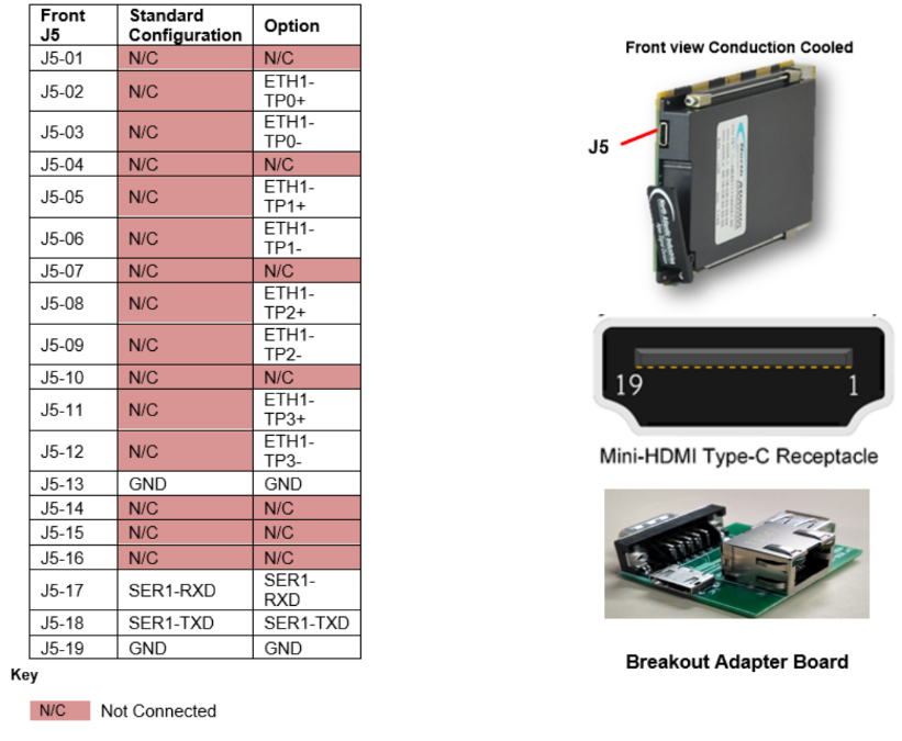
Signal Descriptions J5
| Signal Name | Description |
|---|---|
| ETH1-TPx | Ethernet port 1 signals (4 pair) 10/100/1000 twisted pair signals (Optional - available only if NOT re-directed to rear I/O (see part number configuration options) |
| SER1-TXD | Asynchronous transmit serial data port 1 (out) / RS232 debug/console port only |
| SER1-RXD | Asynchronous received serial data port 1 (in) / RS232 debug/console port only |
| GND | System Ground (return) |
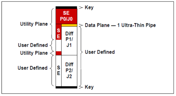
Rear I/O VPX Connectors P0-P2 (Conduction-Cooled)
The 68SR1 3U OpenVPX multifunction I/O board provides interface via the rear VPX connectors.
Rear I/O Summary
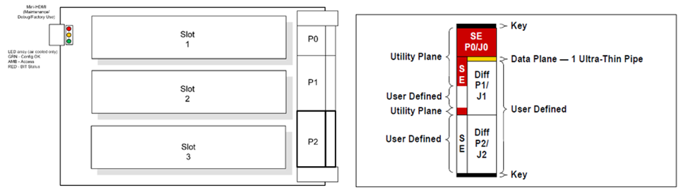
P0 - Utility plane. Contains the following signal definitions:
| Power | Primary +12V, +3.3V_AUX, and System GND |
| Geographical Address Pins | GA0# - GA4#, GAP# |
| Card reset | SYSRST# signal |
| VPX AUX/REF CLK | (Not used) |
P1 - Defined as primarily Data/Control Planes (User defined I/O secondary)
| High Speed Switched Fabric Interface | One ultra-thin pipe option (PCIe ver. 2.0 (x1) or SRIO (1x)). |
| Ethernet | Dual Gig-E port option(s) are available and defined (See Part Number Designation section) |
P2 - User defined I/O (primary)
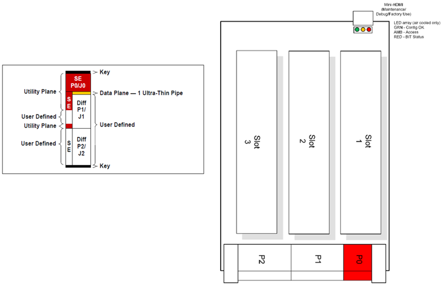
Rear I/O Utility Plane (P0)
The P0 (Utility) Plane contains the primary power, bus and utility signals for the OpenVPX board. Additionally, several of the user defined pins can be utilized for Geographical Addressing and a parallel SYSRST# signal. Signals defined as N/C currently have no functionality associated and is not required for general operation.
| UTILITY | Row | Row | Row | Row | Row | Row | Row |
| P0 | G | F | E | D | C | B | A |
| 1 | (+)12V (VS1) | (+)12V (VS1) | (+)12V (VS1) | N/C (NCD1) | N/C (VS2) | N/C (VS2) | N/C (VS2) |
| 2 | (+)12V (VS1) | (+)12V (VS1) | (+)12V (VS1) | N/C (NCD2) | N/C (VS2) | N/C (VS2) | N/C (VS2) |
| 3 | N/C (VS3) | N/C (VS3) | N/C (VS3) | N/C (NCD3) | N/C (VS3) | N/C (VS3) | N/C (VS3) |
| 4 | IMPB-SCL-B (N/C) | IMPB-SDA-B (N/C) | GND | N/C (-12V-AUX) | GND | SYSRST# | NVMRO (N/C) |
| 5 | GAP# | GA4# | GND | (+)3.3V (+3.3V-AUX) | GND | IMPB-SCL-A (N/C) | IMPB-SDA-A (N/C) |
| 6 | GA3# | GA2# | GND | N/C (+12V-AUX) | GND | GA1# | GA0# |
| 7 | N/C (TCK) | GND | N/C (TDO) | N/C (TDI) | GND | N/C (TMS) | N/C (TRST) |
| 8 | GND | (REFCLK-25MHz-) | (REFCLK-25MHz+) | GND | N/C (AUX-CLK-) | N/C (AUX-CLK+) | GND |
| = Motherboard reserved | |
| = Maintenance reserved |
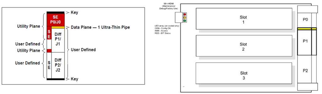
Rear I/O Data/Control Planes (P1)
The 68SR1 has the configuration option for specifying a high-speed serial interface fabric bus connections - PCIe ver. 2.0 (x1). As defined in the OpenVPX bridge or payload slot specifications, the 68SR1 requires only one ‘ultra-thin pipe’ (one Tx and one Rx differential pair), which provides additional user I/O definition opportunity. Additionally, the 68SR1 can be commanded/controlled via dual port Gig-E (options for either 10/100/1000Base-T and/or 1000Base-KX (SerDes) Interfaces). Additional module I/O is also defined on the P1 user defined plane. Signals defined as N/C currently have no functionality associated or are considered optional and are not required for general operation.
| Data Plane | Row | Row | Row | Row | Row | Row | Row |
| P1 | G | F | E | D | C | B | A |
| 1 | GDiscrete1 | GND | PCIE1-SRIO-TXN | PCIE1-SRIO-TXP | GND | PCIE1-SRIO-RXN | PCIE1-SRIO-RXP |
| 2 | GND | IO-D-MOD3N | IO-D-MOD3P | GND | IO-D-MOD3N | IO-D-MOD3P | GND |
| 3 | N/C | GND | IO-D-MOD3N | IO-D-MOD3P | GND | IO-D-MOD3N | IO-D-MOD3P |
| 4 | GND | IO-C-MOD3N | IO-C-MOD3P | GND | IO-C-MOD3N | IO-C-MOD3P | GND |
| 5 | N/C | GND | IO-C-MOD3N | IO-C-MOD3P | GND | IO-C-MOD3N | IO-C-MOD3P |
| 6 | GND | IO-C-MOD3N | IO-C-MOD3P | GND | IO-C-MOD3N | IO-C-MOD3P | GND |
| 7 | N/C | GND | IO-B-MOD3N | IO-B-MOD3P | GND | IO-B-MOD3N | IO-B-MOD3P |
| 8 | IO-B-MOD3N | IO-B-MOD3P | GND | IO-B-MOD3N | IO-B-MOD3P | GND | |
| 9 | SER-RXD1 | GND | IO-A-MOD3N | IO-A-MOD3P | GND | IO-B-MOD3N | IO-B-MOD3P |
| 10 | GND | IO-A-MOD3N | IO-A-MOD3P | GND | IO-A-MOD3N | IO-A-MOD3P | GND |
| 11 | SER-TXD1 | GND | IO-A-MOD3N | IO-A-MOD3P | GND | IO-A-MOD3N | IO-A-MOD3P |
| 12 | GND | IO-A-MOD2P | IO-A-MOD2N | GND | IO-A-MOD2P | IO-A-MOD2N | GND |
| 13 | SER-GND | GND | IO-A-MOD2P | IO-A-MOD2N | GND | IO-A-MOD2P | IO-A-MOD2N |
| 14 | GND | N/C | N/C | GND | IO-A-MOD2P | IO-A-MOD2N | GND |
| 15 | N/C | GND | ETH-TP3N | ETH-TP3P | GND | ETH-TP2N | ETH-TP2P |
| 16 | GND | ETH-TP1N | ETH-TP1P | GND | ETH-TP0N | ETH-TP0P | GND |
| ETH-TXN | ETH-TXP | ETH-RXN | ETH-RXP |
N/C: Pin function(s) are undefined (consider as “no connect”)
| = PCIe (x1) | = MOD 2 IO | = MOD 3 IO | |||
| = Motherboard reserved | = RS232 Console/Debug | = 10/100/1000Base-T (Option) | |||
| = 1000Base-KX (Option) |
USER I/O - Defined Area (User Defined I/O) (P2)
The following pages contain the ‘user defined’ I/O data area front and rear panel pin-outs with their respective signal designations for all module types currently offered/configured for the 68SR1 platform. The card is designed to route the function module I/O signals to the front and rear I/O connector. The following I/O connector pin-out is based upon the function module designated in the module slot. Signals defined as N/C currently have no functionality associated or are considered optional and are not required for general operation.
| Data Plane | Row | Row | Row | Row | Row | Row | Row |
| P1 | G | F | E | D | C | B | A |
| 1 | IO-B-MOD2P | GND | IO-B-MOD2P | IO-B-MOD2N | GND | IO-B-MOD2P | IO-B-MOD2N |
| 2 | GND | IO-B-MOD2P | IO-B-MOD2N | GND | IO-B-MOD2P | IO-B-MOD2N | GND |
| 3 | IO-B-MOD2N | GND | IO-C-MOD2P | IO-C-MOD2N | GND | IO-C-MOD2P | IO-C-MOD2N |
| 4 | GND | IO-C-MOD2P | IO-C-MOD2N | GND | IO-C-MOD2P | IO-C-MOD2N | GND |
| 5 | IO-D-MOD2P | GND | IO-C-MOD2P | IO-C-MOD2N | GND | IO-D-MOD2P | IO-D-MOD2N |
| 6 | GND | IO-D-MOD2P | IO-D-MOD2N | GND | IO-D-MOD2P | IO-D-MOD2N | GND |
| 7 | IO-D-MOD2N | GND | IO-D-MOD2P | IO-D-MOD2N | GND | IO-A-MOD1P | IO-A-MOD1N |
| 8 | GND | IO-A-MOD1P | IO-A-MOD1N | GND | IO-A-MOD1P | IO-A-MOD1N | GND |
| 9 | IO-B-MOD1P | GND | IO-A-MOD1P | IO-A-MOD1N | GND | IO-A-MOD1P | IO-A-MOD1N |
| 10 | GND | IO-B-MOD1P | IO-B-MOD1N | GND | IO-B-MOD1P | IO-B-MOD1N | GND |
| 11 | IO-B-MOD1N | GND | IO-B-MOD1P | IO-B-MOD1N | GND | IO-B-MOD1P | IO-B-MOD1N |
| 12 | GND | IO-C-MOD1P | IO-C-MOD1N | GND | IO-C-MOD1P | IO-C-MOD1N | GND |
| 13 | N/C | GND | IO-C-MOD1P | IO-C-MOD1N | GND | IO-C-MOD1P | IO-C-MOD1N |
| 14 | GND | IO-C-MOD1P | IO-C-MOD1N | GND | IO-D-MOD1P | IO-D-MOD1N | GND |
| 15 | N/C | GND | IO-D-MOD1P | IO-D-MOD1N | GND | IO-D-MOD1P | IO-D-MOD1N |
| 16 | GND | IO-D-MOD1P | IO-D-MOD1N | GND | IO-D-MOD1P | IO-D-MOD1N | GND |
N/C: Pin function(s) are undefined (consider as “no connect”)
| = MOD 1 IO | = MOD 2 IO |
MECHANICAL DETAILS
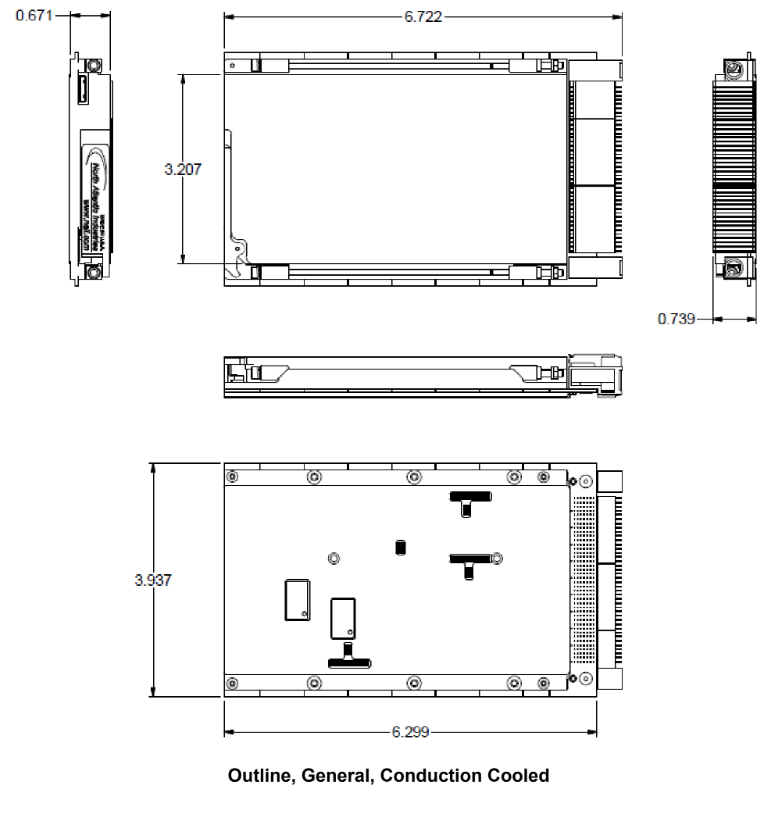
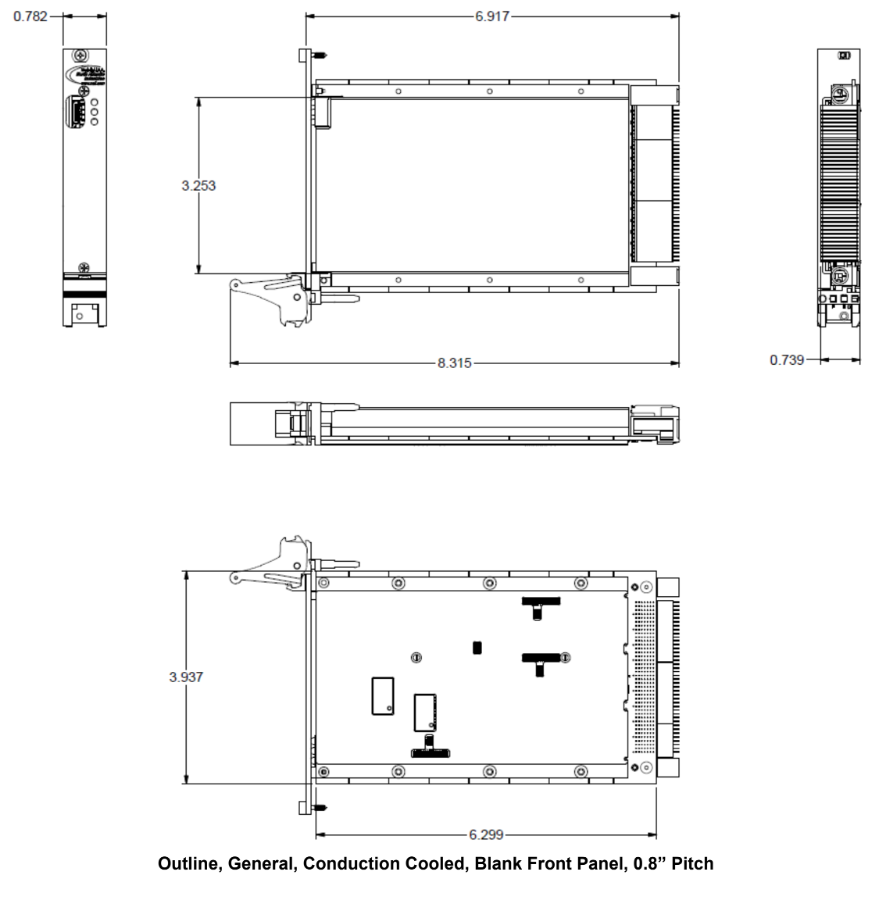
General - Outline
Note
The following mechanical outline detail examples are provided for reference only. Dimensions are in inches unless otherwise specified.
Conduction Cooled
Convection Cooled
68SR1 PART NUMBER DESIGNATION
| Standard Product: 68SR1-AAABBBCCCMTEHI |
|---|
| PROD ID | M1 | M2 | M3 | MECH | TEMP | ETH | HSI | IPMC | Configuration and Option Descriptions |
| 68SR1- | 3U OpenVPX Solid-State Power Controller Relay Board 1x PCIe x1 Data Plane Interface 1x 10/100/1000BASE-T (or 1000BASE-KX) Ethernet 3x COSA Solid-State Power Switch (SWx) Module Slots | ||||||||
| AAA | Module Slot 1 (M1) (See Available Function Modules) Z00 = No Module (See Note 1) | ||||||||
| BBB | Module Slot 2 (M2) (See Available Function Modules) Z00 = No Module (See Note 1) | ||||||||
| CCC | Module Slot 3 (M3) (See Available Function Modules) Z00 = No Module (See Note 1) | ||||||||
| M | Mechanical Options P = Blank Front Panel, (4HP, 0.8" pitch) and Rear I/O K = Blank Front Panel (5HP, 1.0" pitch) and Rear I/O W = Conduction Cooled with Wedgelocks | ||||||||
| T | Temperature/Environmental Options (All boards are Conformal Coated) C = 0ᵒC – 70ᵒC H = -40ᵒC – 85ᵒC | ||||||||
| E | Ethernet Options 0 = No Ethernet 1 = MB Port A (10/100/1000Base-T) to Front 2 = MB Port A (10/100/1000Base-T) to Rear A = MB Port A (1000Base-KX (SerDes) Interface) to Rear | ||||||||
| H | High Speed Serial Switched Fabric Interface 0 = None (Ethernet Only) 5 = PCIe (x1, P1 wafer row-1, default) | ||||||||
| I | IPMC Option (See Note 2) 0 = None 1 = IPMC (VITA 46.11 Tier 2 compliant; basic) |
Specifications are subject to change without notice.
NOTES
| 1 | Module Slot 1 - 3 (AAA – CCC) (See Available Function Modules, Module ID) |
| 2 | IPMC Definition 0. OPTION “0”: DEFAULT. The board will not provide IPMC functionality. The board in this default configuration will boot normally without a Chassis Manager being present. 1. OPTION “1”: The board will provide VITA 46.11 Tier 2 compliant basic IPMC functionality. The board will be configured expecting Chassis Manager communication on boot-up and requires the +3.3V-AUX power supply (PS) to be available on the backplane (provision of +3.3V-AUX is a VPX requirement). |
AVAILABLE FUNCTION MODULES
| Module ID / Type | # of Channels | Description |
|---|---|---|
| SW1 | 4 | Normally Open (NO), Low-V, ±100V @ 6A continuous (max./Ch.) |
| SW2 | 4 | Normally Open (NO), High-V, ±200V @ 4A continuous (max./Ch.) |
| SW3 | 2 | Normally Closed (NC), Low-V, ±100V @ 3A continuous (max./Ch.) |
SWx SOLID-STATE POWER CONTROLLER/RELAY (SWITCHING MODULES)
The 68SR1 3U OpenVPX configurable open systems architecture motherboard can be configured with up to three different Solid-State Power Controller/Relay (switching) modules types, each capable of supporting up to four isolated high current & voltage discrete output switching channels:
| Module ID / Type | # of Channels | Description |
|---|---|---|
| SW1 | 4 | Normally Open (NO), Low-V, ±100V @ 6A continuous (max./Ch.) |
| SW2 | 4 | Normally Open (NO), High-V, ±200V @ 4A continuous (max./Ch.) |
| SW3 | 2 | Normally Closed (NC), Low-V, ±100V @ 3A continuous (max./Ch.) |
Principle of Operation
The Solid-State Power Switch Function Module (SWx) provides up to 4 independent, isolated, programmable solid-state switch channels that can pass through up to 6A max per channel with +/-200V max. With the switch closed, the current through the switch is monitored. These modules include diode clamping on each channel. Clamping is useful for inductive loads, such as relays and short circuit protection.
All 4 channels are galvanically isolated from each other and from system ground. Each channel’s two-wire connection functions as an isolated voltage sensor or as an isolated bi-directional switch. A channel can control valves mechanical relays, indicators, etc. without concern about grounding. This module provides an automatic background built-in-test (BIT) for each channel. The BIT functions are always enabled and continually check that each channel is functioning properly.
Voltage sensing measures both AC and DC input voltages. When the channel is commanded closed, measurements for current through the switch closure are available.
The module design utilizes state of the art galvanic isolation that is superior to alternatives such as optocoupler devices. The galvanic isolation eliminates typical optocoupler design concerns such as uncertain current transfer ratios, nonlinear transfer functions and temperature/lifetime degradation effects.
Output/Switch Interface
Each channel contains an isolated MOSFET pair, configured as isolated Solid-State Relay (SSR). The SSR is energized, so both AC and DC current can flow through the channels I/O pins. The MOSFET presents a low ~0.5Ω on-impedance. The module contains circuitry to measure the current through the SSR and the voltage present on the I/O pins.
Automatic Background Built-In Test (BIT)/Diagnostic Capability
BIT is always enabled and continually checks the health of each channel. This is accomplished by internal test circuitry that is incorporated into each 2- (or 4-) channel modules. Each channel checks that the command, switch open or switch closed, reflects the actual state of the switch. Additionally, each channel is continuously checked for overcurrent. The overcurrent threshold is programmable for each channel. If the switch is open and current reading is greater than 0A +/- spec tolerance, a BIT error will occur. If the switch is closed and voltage is greater than 0V +/- spec tolerance, a BIT error will occur.
Status and Interrupts
The Solid-State Power Switch Function Module provides registers that indicate faults or events. Refer to “Status and Interrupts Module Manual” for the Principle of Operation description.
Module Common Registers
The Solid-State Power Switch Function Module includes module common registers that provide access to module-level bare metal/FPGA revisions & compile times, unique serial number information, and temperature/voltage/current monitoring. Refer to “Module Common Registers Module Manual” for the detailed information.
Register Descriptions
The register descriptions provide the register name, Type, Data Range, Read or Write information, Initialized Value, a description of the function and, in most cases, a data table.
Solid State Power Switch Output Registers
The Switch Command register commands the switch open or closed. The AC/DC Readings Select register sets the output voltage readings.
| Switch Command | |
| Function: | Opens/closes the switch for each channel. |
| Type: | unsigned binary word (32-bit) |
| Data Range: | 0x0 - 0xF (SW1 / SW2) 0x0 - 0x3 (SW3) |
| Read/Write: | R/W |
| Initialized Value: | 0x0 (all channels open) |
| Operational Settings: | Write a 0 to open the switch; write a 1 to close the switch. |
| D31 | D30 | D29 | D28 | D27 | D26 | D25 | D24 | D23 | D22 | D21 | D20 | D19 | D18 | D17 | D16 |
| 0 | 0 | 0 | 0 | 0 | 0 | 0 | 0 | 0 | 0 | 0 | 0 | 0 | 0 | 0 | 0 |
| D15 | D14 | D13 | D12 | D11 | D10 | D9 | D8 | D7 | D6 | D5 | D4 | D3 | D2 | D1 | D0 |
| 0 | 0 | 0 | 0 | 0 | 0 | 0 | 0 | 0 | 0 | 0 | 0 | Ch.4 | Ch.3 | Ch.2 | Ch.1 |
| AC/DC Readings Select | |
| Function: | Sets voltage readings as AC or DC. |
| Type: | unsigned binary word (32-bit) |
| Data Range: | 0 or 1 |
| Read/Write: | R/W |
| Initialized Value: | 0x0 (DC) |
| Operational Settings: | Write a 0 to set voltage readings as DC Write a 1 to set voltage readings as AC |
| D31 | D30 | D29 | D28 | D27 | D26 | D25 | D24 | D23 | D22 | D21 | D20 | D19 | D18 | D17 | D16 |
| 0 | 0 | 0 | 0 | 0 | 0 | 0 | 0 | 0 | 0 | 0 | 0 | 0 | 0 | 0 | 0 |
| D15 | D14 | D13 | D12 | D11 | D10 | D9 | D8 | D7 | D6 | D5 | D4 | D3 | D2 | D1 | D0 |
| 0 | 0 | 0 | 0 | 0 | 0 | 0 | 0 | 0 | 0 | 0 | 0 | Ch.4 | Ch.3 | Ch.2 | Ch.1 |
Solid State Power Switch Measurement Registers
The measured voltage and current applied at or across the I/O pins for each channel can be read from the Voltage Reading and Current Reading registers. The measured temperature of the switch can be read from the Temperature register.
| Voltage Reading | |
| Function: | Reads voltage across the P & N pins per channel. |
| Type: | signed binary dword (32-bit) |
| Data Range: | 0xFFFF FC18 - 0x3E8 (SW1 / SW3) 0xFFFF F830 - 0x7D0 (SW2) |
| Read/Write: | R |
| Initialized Value: | N/A |
| Operational Settings: | Value is a signed binary 32-bit word, where LSB = 100 mV. Data is read as 2's complement number. For example, if the voltage word is 0x00F0 (240d), the actual voltage is 24.0 V. |
| D31 | D30 | D29 | D28 | D27 | D26 | D25 | D24 | D23 | D22 | D21 | D20 | D19 | D18 | D17 | D16 |
| D | D | D | D | D | D | D | D | D | D | D | D | D | D | D | D |
| D15 | D14 | D13 | D12 | D11 | D10 | D9 | D8 | D7 | D6 | D5 | D4 | D3 | D2 | D1 | D0 |
| D | D | D | D | D | D | D | D | D | D | D | D | D | D | D | D |
| Current Reading | |
| Function: | Reads current through the I/O pins per individual channel. |
| Type: | signed binary dword (32-bit) |
| Data Range: | 0xFFFF FED4 - 0x12C (SW1) 0xFFFF FF38 - 0xC8 (SW2) 0xFFFF FF6A - 0x96 (SW3) |
| Read/Write: | R |
| Initialized Value: | N/A |
| Operational Settings: | Value is a signed binary 32-bit word, where LSB = 20 mA. Data is read as 2's complement number. For example, if output current reads 0x0064 (100d), the actual current is 2A. |
| D31 | D30 | D29 | D28 | D27 | D26 | D25 | D24 | D23 | D22 | D21 | D20 | D19 | D18 | D17 | D16 |
| D | D | D | D | D | D | D | D | D | D | D | D | D | D | D | D |
| D15 | D14 | D13 | D12 | D11 | D10 | D9 | D8 | D7 | D6 | D5 | D4 | D3 | D2 | D1 | D0 |
| D | D | D | D | D | D | D | D | D | D | D | D | D | D | D | D |
| Temperature | |
| Function: | Measures the temperature of the solid-state power switch. |
| Type: | signed binary dword (32-bit) |
| Data Range: | 0xFFFF FE70 - 0x514 (-40°C - 130°C) |
| Read/Write: | R |
| Initialized Value: | N/A |
| Operational Settings: | Solid-state power switch temperature in degrees Celsius, where LSB = 0.1 ºC. Data is read as 2's complement number. |
| D31 | D30 | D29 | D28 | D27 | D26 | D25 | D24 | D23 | D22 | D21 | D20 | D19 | D18 | D17 | D16 |
| D | D | D | D | D | D | D | D | D | D | D | D | D | D | D | D |
| D15 | D14 | D13 | D12 | D11 | D10 | D9 | D8 | D7 | D6 | D5 | D4 | D3 | D2 | D1 | D0 |
| D | D | D | D | D | D | D | D | D | D | D | D | D | D | D | D |
Solid State Power Switch Control Registers
The registers in this section program the open and close times for the switch, and the programmed delay before those actions occur. Each channel also measures the over/undervoltage values while the switch is set to open. The overcurrent threshold can be set in the Overcurrent Value register.
| Close Time | |
| Function: | Sets the time it will take for the switch to close from an open state. This function is useful for large loads (soft close) to mitigate inrush current. |
| Type: | unsigned binary word (32-bit) |
| Data Range: | 0x0 (immediate) - 0xC8 (200ms) |
| Read/Write: | R/W |
| Initialized Value: | 0x1 (1ms) |
| Operational Settings: | LSB = 1ms. |
| D31 | D30 | D29 | D28 | D27 | D26 | D25 | D24 | D23 | D22 | D21 | D20 | D19 | D18 | D17 | D16 |
| D | D | D | D | D | D | D | D | D | D | D | D | D | D | D | D |
| D15 | D14 | D13 | D12 | D11 | D10 | D9 | D8 | D7 | D6 | D5 | D4 | D3 | D2 | D1 | D0 |
| D | D | D | D | D | D | D | D | D | D | D | D | D | D | D | D |
| Open Time | |
| Function: | Sets the time it will take for the switch to open from a closed state. This function is useful for large loads (soft open) to mitigate inrush current. |
| Type: | unsigned binary word (32-bit) |
| Data Range: | 0x0 (immediate) - 0xC8 (200ms) |
| Read/Write: | R/W |
| Initialized Value: | 0x (1ms) |
| Operational Settings: | LSB = 1ms. |
| D31 | D30 | D29 | D28 | D27 | D26 | D25 | D24 | D23 | D22 | D21 | D20 | D19 | D18 | D17 | D16 |
| D | D | D | D | D | D | D | D | D | D | D | D | D | D | D | D |
| D15 | D14 | D13 | D12 | D11 | D10 | D9 | D8 | D7 | D6 | D5 | D4 | D3 | D2 | D1 | D0 |
| D | D | D | D | D | D | D | D | D | D | D | D | D | D | D | D |
| Overcurrent Value | |
| Function: | Sets the overcurrent value for each channel. |
| Type: | signed binary dword (32-bit) |
| Data Range: | 0x0 - 0x12C (SW1: 6A max) 0x0 - 0xC8 (SW2: 4A max) 0x0 - 0x96 (SW3: 3A max) |
| Read/Write: | R/W |
| Initialized Value: | 0x12C (SW1) 0xC8 (SW2) 0x96 (SW3) |
| Operational Settings: | LSB = 20mA |
| D31 | D30 | D29 | D28 | D27 | D26 | D25 | D24 | D23 | D22 | D21 | D20 | D19 | D18 | D17 | D16 |
| D | D | D | D | D | D | D | D | D | D | D | D | D | D | D | D |
| D15 | D14 | D13 | D12 | D11 | D10 | D9 | D8 | D7 | D6 | D5 | D4 | D3 | D2 | D1 | D0 |
| D | D | D | D | D | D | D | D | D | D | D | D | D | D | D | D |
| Overcurrent Reset | |
| Function: | Resets disabled channels in Overcurrent Latched Status register following an overcurrent condition as measured by the Current Reading register. |
| Type: | unsigned binary word (32-bit) |
| Data Range: | 0x0 to 0xF |
| Read/Write: | W |
| Initialized Value: | 0 |
| Operational Settings: | Write a 1 to reset disabled channels. The FPGA will write a 0 back to the Overcurrent Reset register when reset process is complete. |
| D31 | D30 | D29 | D28 | D27 | D26 | D25 | D24 | D23 | D22 | D21 | D20 | D19 | D18 | D17 | D16 |
| 0 | 0 | 0 | 0 | 0 | 0 | 0 | 0 | 0 | 0 | 0 | 0 | 0 | 0 | 0 | 0 |
| D15 | D14 | D13 | D12 | D11 | D10 | D9 | D8 | D7 | D6 | D5 | D4 | D3 | D2 | D1 | D0 |
| 0 | 0 | 0 | 0 | 0 | 0 | 0 | 0 | 0 | 0 | 0 | 0 | Ch.4 | Ch.3 | Ch.2 | Ch.1 |
| Overvoltage Value (Switch Open) | |
| Function: | Sets the overvoltage threshold value per channel. Applicable when the switch is open. If the measured voltage rises above this value, the status bit for overvoltage will be set. This is an absolute-value comparison. |
| Type: | unsigned binary word (32-bit) |
| Data Range: | 0x0 - 0x3E8 (SW1 / SW3) 0x0 - 0x7D0 (SW2) |
| Read/Write: | R/W |
| Initialized Value: | 0x3E8 (SW1 / SW3: 100V) 0x7D0 (SW2: 200V) |
| Operational Settings: | The switch fault detection circuitry will report a fault in the Overvoltage (Switch Open) register when the measured voltage is above the value set in Overvoltage Value (Switch Open) register. LSB = 100 mV. |
| Undervoltage Value (Switch Open) | |
| Function: | Sets the undervoltage threshold value per channel. Applicable when the switch is open. If the measured voltage drops below this value, the status bit for undervoltage will be set. This is an absolute-value comparison. |
| Type: | unsigned binary word (32-bit) |
| Data Range: | 0x0 - 0x3E8 (SW1 / SW3) 0x0 - 0x7D0 (SW2) |
| Read/Write: | R/W |
| Initialized Value: | 0x5 (0.5V) |
| Operational Settings: | The switch fault detection circuitry will report a fault in the Undervoltage (Switch Open) register when the measured voltage is below the value set in Undervoltage Value (Switch Open) register. LSB = 100 mV. |
| Close Delay Time | |
| Function: | Sets the time delay before the switch will close from an open state. This delay is triggered upon writing to the Switch Command register. |
| Type: | unsigned binary word (32-bit) |
| Data Range: | 0x0 - 0xFFFF FFFF |
| Read/Write: | R/W |
| Initialized Value: | 0x0 (no delay) |
| Operational Settings: | If the value is set to 0 (no delay), the channel will immediately respond when commanded to close. LSB = 1 us. |
| D31 | D30 | D29 | D28 | D27 | D26 | D25 | D24 | D23 | D22 | D21 | D20 | D19 | D18 | D17 | D16 |
| D | D | D | D | D | D | D | D | D | D | D | D | D | D | D | D |
| D15 | D14 | D13 | D12 | D11 | D10 | D9 | D8 | D7 | D6 | D5 | D4 | D3 | D2 | D1 | D0 |
| D | D | D | D | D | D | D | D | D | D | D | D | D | D | D | D |
| Open Delay Time | |
| Function: | Sets the time delay before the switch will open from a closed state. This delay is triggered upon writing to the Switch Command register. |
| Type: | unsigned binary word (32-bit) |
| Data Range: | 0x0 - 0xFFFF FFFF |
| Read/Write: | R/W |
| Initialized Value: | 0x0 (no delay) |
| Operational Settings: | If the value is set to 0 (no delay), the channel will immediately respond when commanded to open. LSB = 1 us. |
| D31 | D30 | D29 | D28 | D27 | D26 | D25 | D24 | D23 | D22 | D21 | D20 | D19 | D18 | D17 | D16 |
| D | D | D | D | D | D | D | D | D | D | D | D | D | D | D | D |
| D15 | D14 | D13 | D12 | D11 | D10 | D9 | D8 | D7 | D6 | D5 | D4 | D3 | D2 | D1 | D0 |
| D | D | D | D | D | D | D | D | D | D | D | D | D | D | D | D |
Module Common Registers
Refer to ‘Module Common Registers Module Manual’ for the register descriptions.
Status and Interrupt Registers
The SWx Module provides registers for BIT, Overcurrent, Warning Temperature, Over-Temperature, Overvoltage (Switch Open), Undervoltage (Switch Open) and Summary status.
BIT Status
There are four registers associated with the BIT Status: Dynamic Status, Latched Status, Interrupt Enable, and Set Edge/Level Interrupt.
| BIT Status | |
| Function: | Sets the corresponding bit associated with the channel's BIT error. |
| Type: | unsigned binary word (32-bits) |
| Data Range: | 0x0000 0000 to 0x0000 000F |
| Read/Write: | R (Dynamic), R/W (Latched, Interrupt Enable, Edge/Level Interrupt) |
| Initialized Value: | 0 |
| BIT Dynamic Status | |||||||||||||||
| BIT Latched Status | |||||||||||||||
| BIT Interrupt Enable | |||||||||||||||
| BIT Set Edge/Level Interrupt | |||||||||||||||
| D31 | D30 | D29 | D28 | D27 | D26 | D25 | D24 | D23 | D22 | D21 | D20 | D19 | D18 | D17 | D16 |
| 0 | 0 | 0 | 0 | 0 | 0 | 0 | 0 | 0 | 0 | 0 | 0 | 0 | 0 | 0 | 0 |
| D15 | D14 | D13 | D12 | D11 | D10 | D9 | D8 | D7 | D6 | D5 | D4 | D3 | D2 | D1 | D0 |
| 0 | 0 | 0 | 0 | 0 | 0 | 0 | 0 | 0 | 0 | 0 | 0 | Ch4 | Ch3 | Ch2 | Ch1 |
Overcurrent Status
There are four registers associated with the Overcurrent Status: Dynamic Status, Latched Status, Interrupt Enable, and Set Edge/Level Interrupt.
| Overcurrent Status | |
| Function: | Sets the corresponding bit associated with the channel's Overcurrent error. |
| Type: | unsigned binary word (32-bits) |
| Data Range: | 0x0000 0000 to 0x0000 000F |
| Read/Write: | R (Dynamic), R/W (Latched, Interrupt Enable, Edge/Level Interrupt) |
| Initialized Value: | 0 |
| Overcurrent Dynamic Status | |||||||||||||||
| Overcurrent Latched Status | |||||||||||||||
| Overcurrent Interrupt Enable | |||||||||||||||
| Overcurrent Set Edge/Level Interrupt | |||||||||||||||
| D31 | D30 | D29 | D28 | D27 | D26 | D25 | D24 | D23 | D22 | D21 | D20 | D19 | D18 | D17 | D16 |
| 0 | 0 | 0 | 0 | 0 | 0 | 0 | 0 | 0 | 0 | 0 | 0 | 0 | 0 | 0 | 0 |
| D15 | D14 | D13 | D12 | D11 | D10 | D9 | D8 | D7 | D6 | D5 | D4 | D3 | D2 | D1 | D0 |
| 0 | 0 | 0 | 0 | 0 | 0 | 0 | 0 | 0 | 0 | 0 | 0 | Ch4 | Ch3 | Ch2 | Ch1 |
Warning Temperature Status
There are four registers associated with the Warning Temperature Status: Dynamic Status, Latched Status, Interrupt Enable, and Set Edge/Level Interrupt.
| Warning Temperature Status | |
| Function: | Sets the corresponding bit associated with the channel's Warning Temperature event. |
| Type: | unsigned binary word (32-bits) |
| Data Range: | 0x0000 0000 to 0x0000 000F |
| Read/Write: | R (Dynamic), R/W (Latched, Interrupt Enable, Edge/Level Interrupt) |
| Initialized Value: | 0 |
| Warning Temperature Dynamic Status | |||||||||||||||
| Warning Temperature Latched Status | |||||||||||||||
| Warning Temperature Interrupt Enable | |||||||||||||||
| Warning Temperature Set Edge/Level Interrupt | |||||||||||||||
| D31 | D30 | D29 | D28 | D27 | D26 | D25 | D24 | D23 | D22 | D21 | D20 | D19 | D18 | D17 | D16 |
| 0 | 0 | 0 | 0 | 0 | 0 | 0 | 0 | 0 | 0 | 0 | 0 | 0 | 0 | 0 | 0 |
| D15 | D14 | D13 | D12 | D11 | D10 | D9 | D8 | D7 | D6 | D5 | D4 | D3 | D2 | D1 | D0 |
| 0 | 0 | 0 | 0 | 0 | 0 | 0 | 0 | 0 | 0 | 0 | 0 | Ch4 | Ch3 | Ch2 | Ch1 |
Over Temperature Status
There are four registers associated with the Over Temperature Status: Dynamic Status, Latched Status, Interrupt Enable, and Set Edge/Level Interrupt.
| Over Temperature Status | |
| Function: | Sets the corresponding bit associated with the channel's Over Temperature error. |
| Type: | unsigned binary word (32-bits) |
| Data Range: | 0x0000 0000 to 0x0000 000F |
| Read/Write: | R (Dynamic), R/W (Latched, Interrupt Enable, Edge/Level Interrupt) |
| Initialized Value: | 0 |
| Over Temperature Dynamic Status | |||||||||||||||
| Over Temperature Latched Status | |||||||||||||||
| Over Temperature Interrupt Enable | |||||||||||||||
| Over Temperature Set Edge/Level Interrupt | |||||||||||||||
| D31 | D30 | D29 | D28 | D27 | D26 | D25 | D24 | D23 | D22 | D21 | D20 | D19 | D18 | D17 | D16 |
| 0 | 0 | 0 | 0 | 0 | 0 | 0 | 0 | 0 | 0 | 0 | 0 | 0 | 0 | 0 | 0 |
| D15 | D14 | D13 | D12 | D11 | D10 | D9 | D8 | D7 | D6 | D5 | D4 | D3 | D2 | D1 | D0 |
| 0 | 0 | 0 | 0 | 0 | 0 | 0 | 0 | 0 | 0 | 0 | 0 | Ch4 | Ch3 | Ch2 | Ch1 |
Overvoltage (Switch Open) Status
There are four registers associated with the Overvoltage (Switch Open) Status: Dynamic Status, Latched Status, Interrupt Enable, and Set Edge/Level Interrupt.
| Overvoltage (Switch Open) Status | |
| Function: | Sets the corresponding bit associated with the channel's Overvoltage (Switch Open) error. |
| Type: | unsigned binary word (32-bits) |
| Data Range: | 0x0000 0000 to 0x0000 000F |
| Read/Write: | R (Dynamic), R/W (Latched, Interrupt Enable, Edge/Level Interrupt) |
| Initialized Value: | 0 |
| Overvoltage (Switch Open) Dynamic Status | |||||||||||||||
| Overvoltage (Switch Open) Latched Status | |||||||||||||||
| Overvoltage (Switch Open) Interrupt Enable | |||||||||||||||
| Overvoltage (Switch Open) Set Edge/Level Interrupt | |||||||||||||||
| D31 | D30 | D29 | D28 | D27 | D26 | D25 | D24 | D23 | D22 | D21 | D20 | D19 | D18 | D17 | D16 |
| 0 | 0 | 0 | 0 | 0 | 0 | 0 | 0 | 0 | 0 | 0 | 0 | 0 | 0 | 0 | 0 |
| D15 | D14 | D13 | D12 | D11 | D10 | D9 | D8 | D7 | D6 | D5 | D4 | D3 | D2 | D1 | D0 |
| 0 | 0 | 0 | 0 | 0 | 0 | 0 | 0 | 0 | 0 | 0 | 0 | Ch4 | Ch3 | Ch2 | Ch1 |
Undervoltage (Switch Open) Status
There are four registers associated with the Undervoltage (Switch Open) Status: Dynamic Status, Latched Status, Interrupt Enable, and Set Edge/Level Interrupt.
| Undervoltage (Switch Open) Status | |
| Function: | Sets the corresponding bit associated with the channel's Undervoltage (Switch Open) error. |
| Type: | unsigned binary word (32-bits) |
| Data Range: | 0x0000 0000 to 0x0000 000F |
| Read/Write: | R (Dynamic), R/W (Latched, Interrupt Enable, Edge/Level Interrupt) |
| Initialized Value: | 0 |
| Undervoltage (Switch Open) Dynamic Status | |||||||||||||||
| Undervoltage (Switch Open) Latched Status | |||||||||||||||
| Undervoltage (Switch Open) Interrupt Enable | |||||||||||||||
| Undervoltage (Switch Open) Set Edge/Level Interrupt | |||||||||||||||
| D31 | D30 | D29 | D28 | D27 | D26 | D25 | D24 | D23 | D22 | D21 | D20 | D19 | D18 | D17 | D16 |
| 0 | 0 | 0 | 0 | 0 | 0 | 0 | 0 | 0 | 0 | 0 | 0 | 0 | 0 | 0 | 0 |
| D15 | D14 | D13 | D12 | D11 | D10 | D9 | D8 | D7 | D6 | D5 | D4 | D3 | D2 | D1 | D0 |
| 0 | 0 | 0 | 0 | 0 | 0 | 0 | 0 | 0 | 0 | 0 | 0 | Ch4 | Ch3 | Ch2 | Ch1 |
Summary Status
There are four registers associated with the BIT Status: Dynamic Status, Latched Status, Interrupt Enable, and Set Edge/Level Interrupt.
| Summary Status | |
| Function: | Sets the corresponding bit when a fault is detected for BIT, Overcurrent, Warning Temperature, Over Temperature, Overvoltage/Undervoltage (Open Switch) on that channel. |
| Type: | unsigned binary word (32-bits) |
| Data Range: | 0x0000 0000 to 0x0000 000F |
| Read/Write: | R (Dynamic), R/W (Latched, Interrupt Enable, Edge/Level Interrupt) |
| Initialized Value: | 0 |
| Summary Dynamic Status | |||||||||||||||
| Summary Latched Status | |||||||||||||||
| Summary Interrupt Enable | |||||||||||||||
| Summary Set Edge/Level Interrupt | |||||||||||||||
| D31 | D30 | D29 | D28 | D27 | D26 | D25 | D24 | D23 | D22 | D21 | D20 | D19 | D18 | D17 | D16 |
| 0 | 0 | 0 | 0 | 0 | 0 | 0 | 0 | 0 | 0 | 0 | 0 | 0 | 0 | 0 | 0 |
| D15 | D14 | D13 | D12 | D11 | D10 | D9 | D8 | D7 | D6 | D5 | D4 | D3 | D2 | D1 | D0 |
| 0 | 0 | 0 | 0 | 0 | 0 | 0 | 0 | 0 | 0 | 0 | 0 | Ch4 | Ch3 | Ch2 | Ch1 |
Function Register Map
KEY
| Configuration/Control |
| Measurement/Status |
| SOLID STATE POWER SWITCH OUTPUT REGISTERS | |||||
| OFFSET | REGISTER NAME | ACCESS | OFFSET | REGISTER NAME | ACCESS |
| 0x1000 | Switch Control Ch 1-4 | R/W | 0x1008 | AC/DC Readings Select Ch 1-4 | R/W |
| SOLID STATE POWER SWITCH MEASUREMENT REGISTERS | |||||
| OFFSET | REGISTER NAME | ACCESS | OFFSET | REGISTER NAME | ACCESS |
| 0x2000 | Voltage Reading Ch 1 | R | 0x2004 | Current Reading Ch 1 | R |
| 0x2100 | Voltage Reading Ch 2 | R | 0x2104 | Current Reading Ch 2 | R |
| 0x2200 | Voltage Reading Ch 3 | R | 0x2204 | Current Reading Ch 3 | R |
| 0x2300 | Voltage Reading Ch 4 | R | 0x2304 | Current Reading Ch 4 | R |
| 0x2008 | Temperature Ch 1 | R | |||
| 0x2108 | Temperature Ch 2 | R | |||
| 0x2208 | Temperature Ch 3 | R | |||
| 0x2308 | Temperature Ch 4 | R | |||
| SOLID STATE POWER SWITCH CONTROL REGISTERS | |||||
| OFFSET | REGISTER NAME | ACCESS | OFFSET | REGISTER NAME | ACCESS |
| 0x200C | Close Time Ch 1 | R/W | 0x2010 | Open Time Ch 1 | R/W |
| 0x210C | Close Time Ch 2 | R/W | 0x2110 | Open Time Ch 2 | R/W |
| 0x220C | Close Time Ch 3 | R/W | 0x2210 | Open Time Ch 3 | R/W |
| 0x230C | Close Time Ch 4 | R/W | 0x2310 | Open Time Ch 4 | R/W |
| 0x2014 | Overcurrent Value Ch 1 | R/W | 0x1004 | Overcurrent Reset Ch 1-4 | R/W |
| 0x2114 | Overcurrent Value Ch 2 | R/W | |||
| 0x2214 | Overcurrent Value Ch 3 | R/W | |||
| 0x2314 | Overcurrent Value Ch 4 | R/W | |||
| 0x2018 | Overvoltage Value (Switch Open) Ch 1 | R/W | 0x201C | Undervoltage Value (Switch Open) Ch 1 | R/W |
| 0x2118 | Overvoltage Value (Switch Open) Ch 2 | R/W | 0x211C | Undervoltage Value (Switch Open) Ch 2 | R/W |
| 0x2218 | Overvoltage Value (Switch Open) Ch 3 | R/W | 0x221C | Undervoltage Value (Switch Open) Ch 3 | R/W |
| 0x2318 | Overvoltage Value (Switch Open) Ch 4 | R/W | 0x231C | Undervoltage Value (Switch Open) Ch 4 | R/W |
| 0x2020 | Close Delay Time Ch 1 | R/W | 0x2024 | Open Delay Time Ch 1 | R/W |
| 0x2120 | Close Delay Time Ch 2 | R/W | 0x2124 | Open Delay Time Ch 2 | R/W |
| 0x2220 | Close Delay Time Ch 3 | R/W | 0x2224 | Open Delay Time Ch 3 | R/W |
| 0x2320 | Close Delay Time Ch 4 | R/W | 0x2324 | Open Delay Time Ch 4 | R/W |
| MODULE COMMON REGISTERS | |||||
| Refer to “Module Common Registers Module Manual” for the Module Common Registers Function Register Map. |
| STATUS REGISTERS* | |||||
| *When an event is detected, the bit associated with the event is set in this register and will remain set until the user clears the event bit. Clearing the bit requires writing a 1 back to the specific bit that was set when read (i.e., write-1-to-clear, writing a “1” to a bit set to “1” will set the bit to “0). | |||||
| OFFSET | REGISTER NAME | ACCESS | OFFSET | REGISTER NAME | ACCESS |
| BIT | Overcurrent | ||||
| 0x0800 | Dynamic Status | R | 0x0810 | Dynamic Status | R |
| 0x0804 | Latched Status* | R/W | 0x0814 | Latched Status* | R/W |
| 0x0808 | Interrupt Enable | R/W | 0x0818 | Interrupt Enable | R/W |
| 0x080C | Set Edge/Level Interrupt | R/W | 0x081C | Set Edge/Level Interrupt | R/W |
| Warning Temperature | Overtemperature | ||||
| 0x0820 | Dynamic Status | R | 0x0830 | Dynamic Status | R |
| 0x0824 | Latched Status* | R/W | 0x0834 | Latched Status* | R/W |
| 0x0828 | Interrupt Enable | R/W | 0x0838 | Interrupt Enable | R/W |
| 0x082C | Set Edge/Level Interrupt | R/W | 0x083C | Set Edge/Level Interrupt | R/W |
| Overvoltage (Switch Open) | Undervoltage (Switch Open) | ||||
| 0x0840 | Dynamic Status | R | 0x0850 | Dynamic Status | R |
| 0x0844 | Latched Status* | R/W | 0x0854 | Latched Status* | R/W |
| 0x0848 | Interrupt Enable | R/W | 0x0858 | Interrupt Enable | R/W |
| 0x084C | Set Edge/Level Interrupt | R/W | 0x085C | Set Edge/Level Interrupt | R/W |
| Summary | |||||
| 0x09A0 | Dynamic Status | R | |||
| 0x09A4 | Latched Status* | R/W | |||
| 0x09A8 | Interrupt Enable | R/W | |||
| 0x09AC | Set Edge/Level Interrupt | R/W | |||
DOCS.NAII REVISIONS
| Revision Date | Description |
|---|---|
| 2026-10-05 | Initial release of 68SR1 board manual. |
STATUS AND INTERRUPTS
Status registers indicate the detection of faults or events. The status registers can be channel bit-mapped or event bit-mapped. An example of a channel bit-mapped register is the BIT status register, and an example of an event bit-mapped register is the FIFO status register.
For those status registers that allow interrupts to be generated upon the detection of the fault or the event, there are four registers associated with each status: Dynamic, Latched, Interrupt Enabled, and Set Edge/Level Interrupt.
Dynamic Status: The Dynamic Status register indicates the current condition of the fault or the event. If the fault or the event is momentary, the contents in this register will be clear when the fault or the event goes away. The Dynamic Status register can be polled, however, if the fault or the event is sporadic, it is possible for the indication of the fault or the event to be missed.
Latched Status: The Latched Status register indicates whether the fault or the event has occurred and keeps the state until it is cleared by the user. Reading the Latched Status register is a better alternative to polling the Dynamic Status register because the contents of this register will not clear until the user commands to clear the specific bit(s) associated with the fault or the event in the Latched Status register. Once the status register has been read, the act of writing a 1 back to the applicable status register to any specific bit (channel/event) location will “clear” the bit (set the bit to 0). When clearing the channel/event bits, it is strongly recommended to write back the same bit pattern as read from the Latched Status register. For example, if the channel bit-mapped Latched Status register contains the value 0x0000 0005, which indicates fault/event detection on channel 1 and 3, write the value 0x0000 0005 to the Latched Status register to clear the fault/event status for channel 1 and 3. Writing a “1” to other channels that are not set (example 0x0000 000F) may result in incorrectly “clearing” incoming faults/events for those channels (example, channel 2 and 4).
Interrupt Enable: If interrupts are preferred upon the detection of a fault or an event, enable the specific channel/event interrupt in the Interrupt Enable register. The bits in Interrupt Enable register map to the same bits in the Latched Status register. When a fault or event occurs, an interrupt will be fired. Subsequent interrupts will not trigger until the application acknowledges the fired interrupt by clearing the associated channel/event bit in the Latched Status register. If the interruptible condition is still persistent after clearing the bit, this may retrigger the interrupt depending on the Edge/Level setting.
Set Edge/Level Interrupt: When interrupts are enabled, the condition on retriggering the interrupt after the Latch Register is “cleared” can be specified as “edge” triggered or “level” triggered. Note, the Edge/Level Trigger also affects how the Latched Register value is adjusted after it is “cleared” (see below).
Edge triggered: An interrupt will be retriggered when the Latched Status register change from low (0) to high (1) state. Uses for edge-triggered interrupts would include transition detections (Low-to-High transitions, High-to-Low transitions) or fault detections. After “clearing” an interrupt, another interrupt will not occur until the next transition or the re-occurrence of the fault again.
Level triggered: An interrupt will be generated when the Latched Status register remains at the high (1) state. Level-triggered interrupts are used to indicate that something needs attention.
Interrupt Vector and Steering
When interrupts are enabled, the interrupt vector associated with the specific interrupt can be programmed with a unique number/identifier defined by the user such that it can be utilized in the Interrupt Service Routine (ISR) to identify the type of interrupt. When an interrupt occurs, the contents of the Interrupt Vector registers is reported as part of the interrupt mechanism. In addition to specifying the interrupt vector, the interrupt can be directed (“steered”) to the native bus or to the application running on the onboard ARM processor.
Interrupt Trigger Types
In most applications, limiting the number of interrupts generated is preferred as interrupts are costly, thus choosing the correct Edge/Level interrupt trigger to use is important.
Example 1: Fault detection
This example illustrates interrupt considerations when detecting a fault like an “open” on a line. When an “open” is detected, the system will receive an interrupt. If the “open” on the line is persistent and the trigger is set to “edge”, upon “clearing” the interrupt, the system will not regenerate another interrupt. If, instead, the trigger is set to “level”, upon “clearing” the interrupt, the system will re-generate another interrupt. Thus, in this case, it will be better to set the trigger type to “edge”.
Example 2: Threshold detection
This example illustrates interrupt considerations when detecting an event like reaching or exceeding the “high watermark” threshold value. In a communication device, when the number of elements received in the FIFO reaches the high-watermark threshold, an interrupt will be generated. Normally, the application would read the count of the number of elements in the FIFO and read this number of elements from the FIFO. After reading the FIFO data, the application would “clear” the interrupt. If the trigger type is set to “edge”, another interrupt will be generated only if the number of elements in FIFO goes below the “high watermark” after the “clearing” the interrupt and then fills up to reach the “high watermark” threshold value. Since receiving communication data is inherently asynchronous, it is possible that data can continue to fill the FIFO as the application is pulling data off the FIFO. If, at the time the interrupt is “cleared”, the number of elements in the FIFO is at or above the “high watermark”, no interrupts will be generated. In this case, it will be better to set the trigger type to “level”, as the purpose here is to make sure that the FIFO is serviced when the number of elements exceeds the high watermark threshold value. Thus, upon “clearing” the interrupt, if the number of elements in the FIFO is at or above the “high watermark” threshold value, another interrupt will be generated indicating that the FIFO needs to be serviced.
Dynamic and Latched Status Registers Examples
The examples in this section illustrate the differences in behavior of the Dynamic Status and Latched Status registers as well as the differences in behavior of Edge/Level Trigger when the Latched Status register is cleared.
Figure 1. Example of Module's Channel-Mapped Dynamic and Latched Status States
No Clearing of
Latched StatusClearing of Latched Status
(Edge-Triggered)Clearing of Latched Status
(Level-Triggered)Time Dynamic Status Latched Status Action Latched Status Action Latched T0 0x0 0x0 Read Latched Register 0x0 Read Latched Register 0x0 T1 0x1 0x1 Read Latched Register 0x1 0x1 T1 0x1 0x1 Write 0x1 to Latched Register Write 0x1 to Latched Register T1 0x1 0x1 0x0 0x1 T2 0x0 0x1 Read Latched Register 0x0 Read Latched Register 0x1 T2 0x0 0x1 Read Latched Register 0x0 Write 0x1 to Latched Register T2 0x0 0x1 Read Latched Register 0x0 0x0 T3 0x2 0x3 Read Latched Register 0x2 Read Latched Register 0x2 T3 0x2 0x3 Write 0x2 to Latched Register Write 0x2 to Latched Register T3 0x2 0x3 0x0 0x2 T4 0x2 0x3 Read Latched Register 0x1 Read Latched Register 0x3 T4 0x2 0x3 Write 0x1 to Latched Register Write 0x3 to Latched Register T4 0x2 0x3 0x0 0x2 T5 0xC 0xF Read Latched Register 0xC Read Latched Register 0xE T5 0xC 0xF Write 0xC to Latched Register Write 0xE to Latched Register T5 0xC 0xF 0x0 0xC T6 0xC 0xF Read Latched Register 0x0 Read Latched 0xC T6 0xC 0xF Read Latched Register 0x0 Write 0xC to Latched Register T6 0xC 0xF Read Latched Register 0x0 0xC T7 0x4 0xF Read Latched Register 0x0 Read Latched Register 0xC T7 0x4 0xF Read Latched Register 0x0 Write 0xC to Latched Register T7 0x4 0xF Read Latched Register 0x0 0x4 T8 0x4 0xF Read Latched Register 0x0 Read Latched Register 0x4 Interrupt Examples
The examples in this section illustrate the interrupt behavior with Edge/Level Trigger.
Figure 2. Illustration of Latched Status State for Module with 4-Channels with Interrupt Enabled
Time Latched Status
(Edge-Triggered -
Clear Multi-Channel)Latched Status
(Edge-Triggered -
Clear Single Channel)Latched Status
(Level-Triggered -
Clear Multi-Channel)Action Latched Action Latched Action Latched T1
(Int 1)Interrupt Generated
Read Latched Registers0x1 Interrupt Generated
Read Latched Registers0x1 Interrupt Generated
Read Latched Registers0x1 T1
(Int 1)Write 0x1 to Latched Register Write 0x1 to Latched Register Write 0x1 to Latched Register T1
(Int 1)0x0 0x0 Interrupt re-triggers
Note, interrupt re-triggers after
each clear until T2.0x1 T3
(Int 2)Interrupt Generated
Read Latched Registers0x2 Interrupt Generated
Read Latched Registers0x2 Interrupt Generated
Read Latched Registers0x2 T3
(Int 2)Write 0x2 to Latched Register Write 0x2 to Latched Register Write 0x2 to Latched Register T3
(Int 2)0x0 0x0 Interrupt re-triggers
Note, interrupt re-triggers after
each clear until T7.0x2 T4
(Int 3)Interrupt Generated
Read Latched Registers0x1 Interrupt Generated
Read Latched Registers0x1 Interrupt Generated
Read Latched Registers0x3 T4
(Int 3)Write 0x1 to Latched Register Write 0x1 to Latched Register Write 0x3 to Latched Register T4
(Int 3)0x0 0x0 Interrupt re-triggers
Note, interrupt re-triggers after
each clear and 0x3 is reported
in Latched Register until T5.0x3 T4
(Int 3)0x0 0x0 Interrupt re-triggers
Note, interrupt re-triggers after
each clear until T7.0x2 T6
(Int 4)Interrupt Generated
Read Latched Registers0xC Interrupt Generated
Read Latched Registers0xC Interrupt Generated
Read Latched Registers0xE T6
(Int 4)Write 0xC to Latched Register Write 0x4 to Latched Register Write 0xE to Latched Register T6
(Int 4)0x0 Interrupt re-triggers
Write 0x8 to Latched Register0x8 Interrupt re-triggers
Note, interrupt re-triggers after
each clear and 0xE is
reported in Latched Register until T7.0xE T6
(Int 4)0x0 0x0 Interrupt re-triggers
Note, interrupt re-triggers after
each clear and 0xC is
reported in Latched Register until T8.0xC T6
(Int 4)0x0 0x0 Interrupt re-triggers
Note, interrupt re-triggers after
each clear and 0x4 is
reported in Latched Register always.0x4 REVISION HISTORY
Motherboard Manual - Status and Interrupts Revision History Revision Revision Date Description C 2021-11-30 C08896; Transition manual to docbuilder format - no technical info change. Link to original
DOCS.NAII REVISIONS Revision Date Description 2026-03-02 Formatting updates to document; no technical changes. 2026-05-18 Fixed formatting issues from conversion to new doc site format. 2026-05-19 Fixed minor formatting issue with Interrupt Examples table structure (removed extraneous cell). 2026-07-15 Revised image files for image quality.
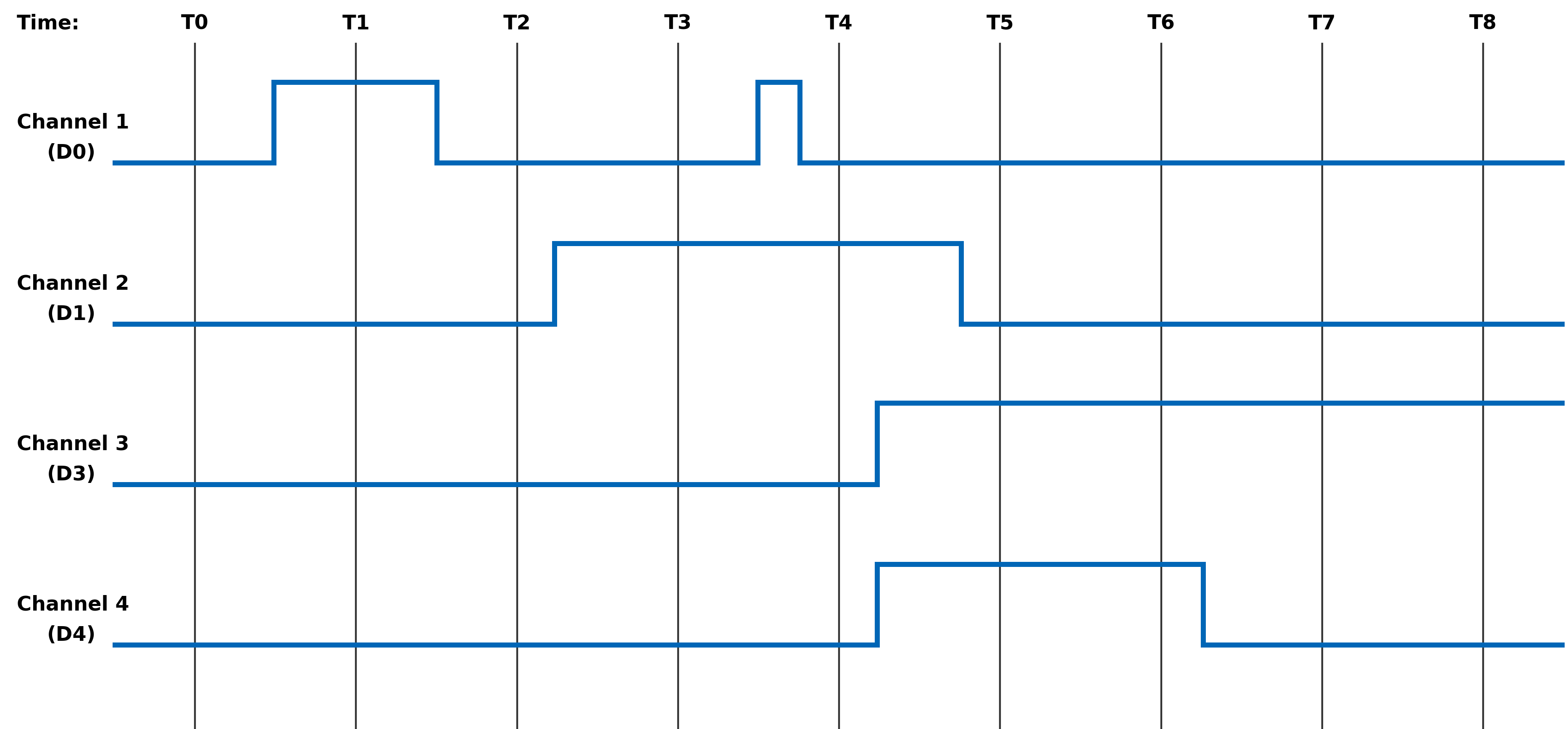
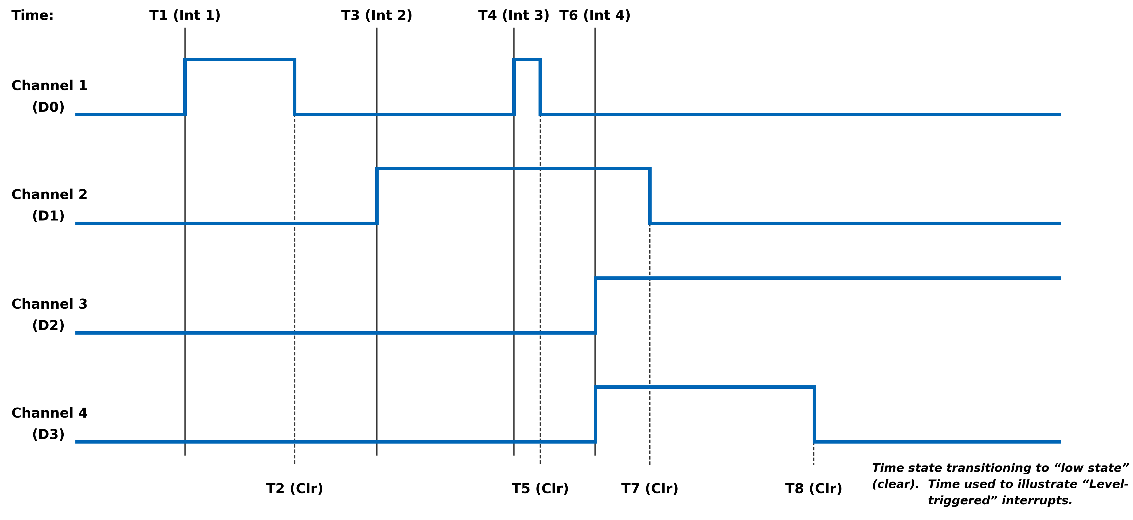
MODULE COMMON REGISTERS
The registers described in this document are common to all NAI Generation 5 modules.
Module Information Registers
The registers in this section provide module information such as firmware revisions, capabilities and unique serial number information.
FPGA Version Registers
The FPGA firmware version registers include registers that contain the Revision, Compile Timestamp, SerDes Revision, Template Revision and Zynq Block Revision information.
FPGA Revision Function: FPGA firmware revision Type: unsigned binary word (32-bit) Data Range: 0x0000 0000 to 0xFFFF FFFF Read/Write: R Initialized Value: Value corresponding to the revision of the board's FPGA Operational Settings: The upper 16-bits are the major revision and the lower 16-bits are the minor revision.
D31 D30 D29 D28 D27 D26 D25 D24 D23 D22 D21 D20 D19 D18 D17 D16 Major Revision Number D15 D14 D13 D12 D11 D10 D9 D8 D7 D6 D5 D4 D3 D2 D1 D0 Minor Revision Number
FPGA Compile Timestamp Function: Compile Timestamp for the FPGA firmware. Type: unsigned binary word (32-bit) Data Range: N/A Read/Write: R Initialized Value: Value corresponding to the compile timestamp of the board's FPGA Operational Settings: The 32-bit value represents the Day, Month, Year, Hour, Minutes and Seconds as formatted in the table:
D31 D30 D29 D28 D27 D26 D25 D24 D23 D22 D21 D20 D19 D18 D17 D16 day (5-bits) month (4-bits) year (6-bits) hr D15 D14 D13 D12 D11 D10 D9 D8 D7 D6 D5 D4 D3 D2 D1 D0 hour (5-bits) minutes (6-bits) seconds (6-bits)
FPGA SerDes Revision Function: FPGA SerDes revision Type: unsigned binary word (32-bit) Data Range: 0x0000 0000 to 0xFFFF FFFF Read/Write: R Initialized Value: Value corresponding to the SerDes revision of the board's FPGA Operational Settings: The upper 16-bits are the major revision, and the lower 16-bits are the minor revision.
D31 D30 D29 D28 D27 D26 D25 D24 D23 D22 D21 D20 D19 D18 D17 D16 Major Revision Number D15 D14 D13 D12 D11 D10 D9 D8 D7 D6 D5 D4 D3 D2 D1 D0 Minor Revision Number
FPGA Template Revision Function: FPGA Template revision Type: unsigned binary word (32-bit) Data Range: 0x0000 0000 to 0xFFFF FFFF Read/Write: R Initialized Value: Value corresponding to the template revision of the board's FPGA Operational Settings: The upper 16-bits are the major revision, and the lower 16-bits are the minor revision.
D31 D30 D29 D28 D27 D26 D25 D24 D23 D22 D21 D20 D19 D18 D17 D16 Major Revision Number D15 D14 D13 D12 D11 D10 D9 D8 D7 D6 D5 D4 D3 D2 D1 D0 Minor Revision Number
FPGA Zynq Block Revision Function: FPGA Zynq Block revision Type: unsigned binary word (32-bit) Data Range: 0x0000 0000 to 0xFFFF FFFF Read/Write: R Initialized Value: Value corresponding to the Zynq block revision of the board's FPGA Operational Settings: The upper 16-bits are the major revision, and the lower 16-bits are the minor revision.
D31 D30 D29 D28 D27 D26 D25 D24 D23 D22 D21 D20 D19 D18 D17 D16 Major Revision Number D15 D14 D13 D12 D11 D10 D9 D8 D7 D6 D5 D4 D3 D2 D1 D0 Minor Revision Number Bare Metal Version Registers
The Bare Metal firmware version registers include registers that contain the Revision and Compile Time information.
Bare Metal Revision Function: Bare Metal firmware revision Type: unsigned binary word (32-bit) Data Range: 0x0000 0000 to 0xFFFF FFFF Read/Write: R Initialized Value: Value corresponding to the revision of the board's Bare Metal Operational Settings: The upper 16-bits are the major revision and the lower 16-bits are the minor revision.
D31 D30 D29 D28 D27 D26 D25 D24 D23 D22 D21 D20 D19 D18 D17 D16 Major Revision Number D15 D14 D13 D12 D11 D10 D9 D8 D7 D6 D5 D4 D3 D2 D1 D0 Minor Revision Number
Bare Metal Compile Time Function: Provides an ASCII representation of the Date/Time for the Bare Metal compile time. Type: 24-character ASCII string - Six (6) unsigned binary word (32-bit) Data Range: N/A Read/Write: R Initialized Value: Value corresponding to the ASCII representation of the compile time of the board's Bare Metal Operational Settings: The six 32-bit words provide an ASCII representation of the Date/Time. The hexadecimal values in the field below represent: May 17 2019 at 15:38:32 Note
little-endian order of ASCII values
Word 1 (Ex. 0x2079614D) D31 D30 D29 D28 D27 D26 D25 D24 D23 D22 D21 D20 D19 D18 D17 D16 Space (0x20) Month ('y' - 0x79) D15 D14 D13 D12 D11 D10 D9 D8 D7 D6 D5 D4 D3 D2 D1 D0 Month ('a' - 0x61) Month ('M' - 0x4D) Word 2 (Ex. 0x32203731) D31 D30 D29 D28 D27 D26 D25 D24 D23 D22 D21 D20 D19 D18 D17 D16 Year ('2' - 0x32) Space (0x20) D15 D14 D13 D12 D11 D10 D9 D8 D7 D6 D5 D4 D3 D2 D1 D0 Day ('7' - 0x37) Day ('1' - 0x31) Word 3 (Ex. 0x20393130) D31 D30 D29 D28 D27 D26 D25 D24 D23 D22 D21 D20 D19 D18 D17 D16 Space (0x20) Year ('9' - 0x39) D15 D14 D13 D12 D11 D10 D9 D8 D7 D6 D5 D4 D3 D2 D1 D0 Year ('1' - 0x31) Year ('0' - 0x30) Word 4 (Ex. 0x31207461) D31 D30 D29 D28 D27 D26 D25 D24 D23 D22 D21 D20 D19 D18 D17 D16 Hour ('1' - 0x31) Space (0x20) D15 D14 D13 D12 D11 D10 D9 D8 D7 D6 D5 D4 D3 D2 D1 D0 'a' (0x74) 't' (0x61) Word 5 (Ex. 0x38333A35) D31 D30 D29 D28 D27 D26 D25 D24 D23 D22 D21 D20 D19 D18 D17 D16 Minute ('8' - 0x38) Minute ('3' - 0x33) D15 D14 D13 D12 D11 D10 D9 D8 D7 D6 D5 D4 D3 D2 D1 D0 ':' (0x3A) Hour ('5' - 0x35) Word 6 (Ex. 0x0032333A) D31 D30 D29 D28 D27 D26 D25 D24 D23 D22 D21 D20 D19 D18 D17 D16 NULL (0x00) Seconds ('2' - 0x32) D15 D14 D13 D12 D11 D10 D9 D8 D7 D6 D5 D4 D3 D2 D1 D0 Seconds ('3' - 0x33) ':' (0x3A) FSBL Version Registers
The FSBL version registers include registers that contain the Revision and Compile Time information for the First Stage Boot Loader (FSBL).
FSBL Revision Function: FSBL firmware revision Type: unsigned binary word (32-bit) Data Range: 0x0000 0000 to 0xFFFF FFFF Read/Write: R Initialized Value: Value corresponding to the revision of the board's FSBL Operational Settings: The upper 16-bits are the major revision, and the lower 16-bits are the minor revision.
D31 D30 D29 D28 D27 D26 D25 D24 D23 D22 D21 D20 D19 D18 D17 D16 Major Revision Number D15 D14 D13 D12 D11 D10 D9 D8 D7 D6 D5 D4 D3 D2 D1 D0 Minor Revision Number
FSBL Compile Time Function: Provides an ASCII representation of the Date/Time for the FSBL compile time. Type: 24-character ASCII string - Six (6) unsigned binary word (32-bit) Data Range: N/A Read/Write: R Initialized Value: Value corresponding to the ASCII representation of the Compile Time of the board's FSBL Operational Settings: The six 32-bit words provide an ASCII representation of the Date/Time. The hexadecimal values in the field below represent: May 17 2019 at 15:38:32
Note
little-endian order of ASCII values
Word 1 (Ex. 0x2079614D) D31 D30 D29 D28 D27 D26 D25 D24 D23 D22 D21 D20 D19 D18 D17 D16 Space (0x20) Month ('y' - 0x79) D15 D14 D13 D12 D11 D10 D9 D8 D7 D6 D5 D4 D3 D2 D1 D0 Month ('a' - 0x61) Month ('M' - 0x4D) Word 2 (Ex. 0x32203731) D31 D30 D29 D28 D27 D26 D25 D24 D23 D22 D21 D20 D19 D18 D17 D16 Year ('2' - 0x32) Space (0x20) D15 D14 D13 D12 D11 D10 D9 D8 D7 D6 D5 D4 D3 D2 D1 D0 Day ('7' - 0x37) Day ('1' - 0x31) Word 3 (Ex. 0x20393130) D31 D30 D29 D28 D27 D26 D25 D24 D23 D22 D21 D20 D19 D18 D17 D16 Space (0x20) Year ('9' - 0x39) D15 D14 D13 D12 D11 D10 D9 D8 D7 D6 D5 D4 D3 D2 D1 D0 Year ('1' - 0x31) Year ('0' - 0x30) Word 4 (Ex. 0x31207461) D31 D30 D29 D28 D27 D26 D25 D24 D23 D22 D21 D20 D19 D18 D17 D16 Hour ('1' - 0x31) Space (0x20) D15 D14 D13 D12 D11 D10 D9 D8 D7 D6 D5 D4 D3 D2 D1 D0 'a' (0x74) 't' (0x61) Word 5 (Ex. 0x38333A35) D31 D30 D29 D28 D27 D26 D25 D24 D23 D22 D21 D20 D19 D18 D17 D16 Minute ('8' - 0x38) Minute ('3' - 0x33) D15 D14 D13 D12 D11 D10 D9 D8 D7 D6 D5 D4 D3 D2 D1 D0 ':' (0x3A) Hour ('5' - 0x35) Word 6 (Ex. 0x0032333A) D31 D30 D29 D28 D27 D26 D25 D24 D23 D22 D21 D20 D19 D18 D17 D16 NULL (0x00) Seconds ('2' - 0x32) D15 D14 D13 D12 D11 D10 D9 D8 D7 D6 D5 D4 D3 D2 D1 D0 Seconds ('3' - 0x33) ':' (0x3A) Module Serial Number Registers
The Module Serial Number registers include registers that contain the Serial Numbers for the Interface Board and the Functional Board of the module.
Interface Board Serial Number Function: Unique 128-bit identifier used to identify the interface board. Type: 16-character ASCII string - Four (4) unsigned binary words (32-bit) Data Range: N/A Read/Write: R Initialized Value: Serial number of the interface board Operational Settings: This register is for information purposes only.
Functional Board Serial Number Function: Unique 128-bit identifier used to identify the functional board. Type: 16-character ASCII string - Four (4) unsigned binary words (32-bit) Data Range: N/A Read/Write: R Initialized Value: Serial number of the functional board Operational Settings: This register is for information purposes only.
Module Capability Function: Provides indication for whether or not the module can support the following: SerDes block reads, SerDes FIFO block reads, SerDes packing (combining two 16-bit values into one 32-bit value) and floating point representation. The purpose for block access and packing is to improve the performance of accessing larger amounts of data over the SerDes interface. Type: unsigned binary word (32-bit) Data Range: 0x0000 0000 to 0x0000 0107 Read/Write: R Initialized Value: 0x0000 0107 Operational Settings: A “1” in the bit associated with the capability indicates that it is supported.
D31 D30 D29 D28 D27 D26 D25 D24 D23 D22 D21 D20 D19 D18 D17 D16 0 0 0 0 0 0 0 0 0 0 0 0 0 0 0 0 D15 D14 D13 D12 D11 D10 D9 D8 D7 D6 D5 D4 D3 D2 D1 D0 0 0 0 0 0 0 0 Flt-Pt 0 0 0 0 0 Pack FIFO Blk Blk
Module Memory Map Revision Function: Module Memory Map revision Type: unsigned binary word (32-bit) Data Range: 0x0000 0000 to 0xFFFF FFFF Read/Write: R Initialized Value: Value corresponding to the Module Memory Map Revision Operational Settings: The upper 16-bits are the major revision and the lower 16-bits are the minor revision.
D31 D30 D29 D28 D27 D26 D25 D24 D23 D22 D21 D20 D19 D18 D17 D16 Major Revision Number D15 D14 D13 D12 D11 D10 D9 D8 D7 D6 D5 D4 D3 D2 D1 D0 Minor Revision Number Module Measurement Registers
The registers in this section provide module temperature measurement information.
Temperature Readings Registers
The temperature registers provide the current, maximum (from power-up) and minimum (from power-up) Zynq and PCB temperatures.
Interface Board Current Temperature Function: Measured PCB and Zynq Core temperatures on Interface Board. Type: signed byte (8-bits) for PCB and signed byte (8-bits) for Zynq core temperatures Data Range: 0x0000 0000 to 0x0000 FFFF Read/Write: R Initialized Value: Value corresponding to the measured PCB and Zynq core temperatures based on the table below Operational Settings: The upper 16-bits are not used, and the lower 16-bits are the PCB and Zynq Core Temperatures. For example, if the register contains the value 0x0000 202C, this represents PCB Temperature = 32° Celsius and Zynq Temperature = 44° Celsius.
D31 D30 D29 D28 D27 D26 D25 D24 D23 D22 D21 D20 D19 D18 D17 D16 0 0 0 0 0 0 0 0 0 0 0 0 0 0 0 0 D15 D14 D13 D12 D11 D10 D9 D8 D7 D6 D5 D4 D3 D2 D1 D0 PCB Temperature Zynq Core Temperature
Functional Board Current Temperature Function: Measured PCB temperature on Functional Board. Type: signed byte (8-bits) for PCB Data Range: 0x0000 0000 to 0x0000 00FF Read/Write: R Initialized Value: Value corresponding to the measured PCB on the table below Operational Settings: The upper 24-bits are not used, and the lower 8-bits are the PCB Temperature. For example, if the register contains the value 0x0000 0019, this represents PCB Temperature = 25° Celsius.
D31 D30 D29 D28 D27 D26 D25 D24 D23 D22 D21 D20 D19 D18 D17 D16 0 0 0 0 0 0 0 0 0 0 0 0 0 0 0 0 D15 D14 D13 D12 D11 D10 D9 D8 D7 D6 D5 D4 D3 D2 D1 D0 0 0 0 0 0 0 0 0 PCB Temperature
Interface Board Maximum Temperature Function: Maximum PCB and Zynq Core temperatures on Interface Board since power-on. Type: signed byte (8-bits) for PCB and signed byte (8-bits) for Zynq core temperatures Data Range: 0x0000 0000 to 0x0000 FFFF Read/Write: R Initialized Value: Value corresponding to the maximum measured PCB and Zynq core temperatures since power-on based on the table below Operational Settings: The upper 16-bits are not used, and the lower 16-bits are the maximum PCB and Zynq Core Temperatures. For example, if the register contains the value 0x0000 5569, this represents maximum PCB Temperature = 85° Celsius and maximum Zynq Temperature = 105° Celsius.
D31 D30 D29 D28 D27 D26 D25 D24 D23 D22 D21 D20 D19 D18 D17 D16 0 0 0 0 0 0 0 0 0 0 0 0 0 0 0 0 D15 D14 D13 D12 D11 D10 D9 D8 D7 D6 D5 D4 D3 D2 D1 D0 PCB Temperature Zynq Core Temperature
Interface Board Minimum Temperature Function: Minimum PCB and Zynq Core temperatures on Interface Board since power-on. Type: signed byte (8-bits) for PCB and signed byte (8-bits) for Zynq core temperatures Data Range: 0x0000 0000 to 0x0000 FFFF Read/Write: R Initialized Value: Value corresponding to the minimum measured PCB and Zynq core temperatures since power-on based on the table below Operational Settings: The upper 16-bits are not used, and the lower 16-bits are the minimum PCB and Zynq Core Temperatures. For example, if the register contains the value 0x0000 D8E7, this represents minimum PCB Temperature = -40° Celsius and minimum Zynq Temperature = -25° Celsius.
D31 D30 D29 D28 D27 D26 D25 D24 D23 D22 D21 D20 D19 D18 D17 D16 0 0 0 0 0 0 0 0 0 0 0 0 0 0 0 0 D15 D14 D13 D12 D11 D10 D9 D8 D7 D6 D5 D4 D3 D2 D1 D0 PCB Temperature Zynq Core Temperature
Functional Board Maximum Temperature Function: Maximum PCB temperature on Functional Board since power-on. Type: signed byte (8-bits) for PCB Data Range: 0x0000 0000 to 0x0000 00FF Read/Write: R Initialized Value: Value corresponding to the measured PCB on the table below Operational Settings: The upper 24-bits are not used, and the lower 8-bits are the PCB Temperature. For example, if the register contains the value 0x0000 0055, this represents PCB Temperature = 85° Celsius.
D31 D30 D29 D28 D27 D26 D25 D24 D23 D22 D21 D20 D19 D18 D17 D16 0 0 0 0 0 0 0 0 0 0 0 0 0 0 0 0 D15 D14 D13 D12 D11 D10 D9 D8 D7 D6 D5 D4 D3 D2 D1 D0 0 0 0 0 0 0 0 0 PCB Temperature
Functional Board Minimum Temperature Function: Minimum PCB temperature on Functional Board since power-on. Type: signed byte (8-bits) for PCB Data Range: 0x0000 0000 to 0x0000 00FF Read/Write: R Initialized Value: Value corresponding to the measured PCB on the table below Operational Settings: The upper 24-bits are not used, and the lower 8-bits are the PCB Temperature. For example, if the register contains the value 0x0000 00D8, this represents PCB Temperature = -40° Celsius.
D31 D30 D29 D28 D27 D26 D25 D24 D23 D22 D21 D20 D19 D18 D17 D16 0 0 0 0 0 0 0 0 0 0 0 0 0 0 0 0 D15 D14 D13 D12 D11 D10 D9 D8 D7 D6 D5 D4 D3 D2 D1 D0 0 0 0 0 0 0 0 0 PCB Temperature Higher Precision Temperature Readings Registers
These registers provide higher precision readings of the current Zynq and PCB temperatures.
Higher Precision Zynq Core Temperature Function: Higher precision measured Zynq Core temperature on Interface Board. Type: signed word (16-bits) for integer part and unsigned word (16-bits) for fractional part Data Range: 0x0000 0000 to 0xFFFF FFFF Read/Write: R Initialized Value: Measured Zynq Core temperature on Interface Board Operational Settings: The upper 16-bits represent the signed integer part of the temperature and the lower 16-bits represent the fractional part of the temperature with the resolution of 1/1000 of degree Celsius. For example, if the register contains the value 0x002B 0271, this represents Zynq Core Temperature = 43.625° Celsius, and value 0xFFF6 0177 represents -10.375° Celsius.
D31 D30 D29 D28 D27 D26 D25 D24 D23 D22 D21 D20 D19 D18 D17 D16 Signed Integer Part of Temperature D15 D14 D13 D12 D11 D10 D9 D8 D7 D6 D5 D4 D3 D2 D1 D0 Fractional Part of Temperature
Higher Precision Interface PCB Temperature Function: Higher precision measured Interface PCB temperature. Type: signed word (16-bits) for integer part and unsigned word (16-bits) for fractional part Data Range: 0x0000 0000 to 0xFFFF FFFF Read/Write: R Initialized Value: Measured Interface PCB temperature Operational Settings: The upper 16-bits represent the signed integer part of the temperature and the lower 16-bits represent the fractional part of the temperature with the resolution of 1/1000 of degree Celsius. For example, if the register contains the value 0x0020 007D, this represents Interface PCB Temperature = 32.125° Celsius, and value 0xFFE8 036B represents -24.875° Celsius.
D31 D30 D29 D28 D27 D26 D25 D24 D23 D22 D21 D20 D19 D18 D17 D16 Signed Integer Part of Temperature D15 D14 D13 D12 D11 D10 D9 D8 D7 D6 D5 D4 D3 D2 D1 D0 Fractional Part of Temperature
Higher Precision Functional PCB Temperature Function: Higher precision measured Functional PCB temperature. Type: signed word (16-bits) for integer part and unsigned word (16-bits) for fractional part Data Range: 0x0000 0000 to 0xFFFF FFFF Read/Write: R Initialized Value: Measured Functional PCB temperature Operational Settings: The upper 16-bits represent the signed integer part of the temperature and the lower 16-bits represent the fractional part of the temperature with the resolution of 1/100 of degree Celsius. For example, if the register contains the value 0x0018 004B, this represents Functional PCB Temperature = 24.75° Celsius, and value 0xFFD9 0019 represents -39.25° Celsius.
D31 D30 D29 D28 D27 D26 D25 D24 D23 D22 D21 D20 D19 D18 D17 D16 Signed Integer Part of Temperature D15 D14 D13 D12 D11 D10 D9 D8 D7 D6 D5 D4 D3 D2 D1 D0 Fractional Part of Temperature Module Health Monitoring Registers
The registers in this section provide module temperature measurement information. If the temperature measurements reaches the Lower Critical or Upper Critical conditions, the module will automatically reset itself to prevent damage to the hardware.
Module Sensor Summary Status Function: The corresponding sensor bit is set if the sensor has crossed any of its thresholds. Type: unsigned binary word (32-bits) Data Range: See table below Read/Write: R Initialized Value: 0 Operational Settings: This register provides a summary for module sensors. When the corresponding sensor bit is set, the Sensor Threshold Status register for that sensor will indicate the threshold condition that triggered the event.
Bit(s) Sensor D31:D6 Reserved D5 Functional Board PCB Temperature D4 Interface Board PCB Temperature D3:D0 Reserved Module Sensor Registers
The registers listed in this section apply to each module sensor listed for the Module Sensor Summary Status register. Each individual sensor register provides a group of registers for monitoring module temperatures readings. From these registers, a user can read the current temperature of the sensor in addition to the minimum and maximum temperature readings since power-up. Upper and lower critical/warning temperature thresholds can be set and monitored from these registers. When a programmed temperature threshold is crossed, the Sensor Threshold Status register will set the corresponding bit for that threshold. The figure below shows the functionality of this group of registers when accessing the Interface Board PCB Temperature sensor as an example.
Sensor Threshold Status Function: Reflects which threshold has been crossed Type: unsigned binary word (32-bits) Data Range: See table below Read/Write: R Initialized Value: 0 Operational Settings: The associated bit is set when the sensor reading exceed the corresponding threshold settings.
Bit(s) Description D31:D4 Reserved D3 Exceeded Upper Critical Threshold D2 Exceeded Upper Warning Threshold D1 Exceeded Lower Critical Threshold D0 Exceeded Lower Warning Threshold
Sensor Current Reading Function: Reflects current reading of temperature sensor Type: Single Precision Floating Point Value (IEEE-754) Data Range: Single Precision Floating Point Value (IEEE-754) Read/Write: R Initialized Value: N/A Operational Settings: The register represents current sensor reading as a single precision floating point value. For example, for a temperature sensor, register value 0x41C6 0000 represents temperature = 24.75° Celsius.
Sensor Minimum Reading Function: Reflects minimum value of temperature sensor since power up Type: Single Precision Floating Point Value (IEEE-754) Data Range: Single Precision Floating Point Value (IEEE-754) Read/Write: R Initialized Value: N/A Operational Settings: The register represents minimum sensor value as a single precision floating point value. For example, for a temperature sensor, register value 0x41C6 0000 represents temperature = 24.75° Celsius.
Sensor Maximum Reading Function: Reflects maximum value of temperature sensor since power up Type: Single Precision Floating Point Value (IEEE-754) Data Range: Single Precision Floating Point Value (IEEE-754) Read/Write: R Initialized Value: N/A Operational Settings: The register represents maximum sensor value as a single precision floating point value. For example, for a temperature sensor, register value 0x41C6 0000 represents temperature = 24.75° Celsius.
Sensor Lower Warning Threshold Function: Reflects lower warning threshold of temperature sensor Type: Single Precision Floating Point Value (IEEE-754) Data Range: Single Precision Floating Point Value (IEEE-754) Read/Write: R/W Initialized Value: Default lower warning threshold (value dependent on specific sensor) Operational Settings: The register represents sensor lower warning threshold as a single precision floating point value. For example, for a temperature sensor, register value 0xC220 0000 represents temperature = -40.0° Celsius.
Sensor Lower Critical Threshold Function: Reflects lower critical threshold of temperature sensor Type: Single Precision Floating Point Value (IEEE-754) Data Range: Single Precision Floating Point Value (IEEE-754) Read/Write: R/W Initialized Value: Default lower critical threshold (value dependent on specific sensor) Operational Settings: The register represents sensor lower critical threshold as a single precision floating point value. For example, for a temperature sensor, register value 0xC25C 0000 represents temperature = -55.0° Celsius.
Sensor Upper Warning Threshold Function: Reflects upper warning threshold of temperature sensor Type: Single Precision Floating Point Value (IEEE-754) Data Range: Single Precision Floating Point Value (IEEE-754) Read/Write: R/W Initialized Value: Default upper warning threshold (value dependent on specific sensor) Operational Settings: The register represents sensor upper warning threshold as a single precision floating point value. For example, for a temperature sensor, register value 0x42AA 0000 represents temperature = 85.0° Celsius.
Sensor Upper Critical Threshold Function: Reflects upper critical threshold of temperature sensor Type: Single Precision Floating Point Value (IEEE-754) Data Range: Single Precision Floating Point Value (IEEE-754) Read/Write: R/W Initialized Value: Default upper critical threshold (value dependent on specific sensor) Operational Settings: The register represents sensor upper critical threshold as a single precision floating point value. For example, for a temperature sensor, register value 0x42FA 0000 represents temperature = 125.0° Celsius. FUNCTION REGISTER MAP
KEY
Configuration/Control Measurement/Status/Board Information
MODULE INFORMATION REGISTERS OFFSET REGISTER NAME ACCESS OFFSET REGISTER NAME ACCESS 0x003C FPGA Revision R 0x0074 Bare Metal Revision R 0x0030 FPGA Compile Timestamp R 0x0080 Bare Metal Compile Time (Bit 0-31) R 0x0034 FPGA SerDes Revision R 0x0084 Bare Metal Compile Time (Bit 32-63) R 0x0038 FPGA Template Revision R 0x0088 Bare Metal Compile Time (Bit 64-95) R 0x0040 FPGA Zynq Block Revision R 0x008C Bare Metal Compile Time (Bit 96-127) R 0x0090 Bare Metal Compile Time (Bit 128-159) R 0x0094 Bare Metal Compile Time (Bit 160-191) R 0x007C FSBL Revision R 0x00B0 FSBL Compile Time (Bit 0-31) R 0x00B4 FSBL Compile Time (Bit 32-63) R 0x00B8 FSBL Compile Time (Bit 64-95) R 0x00BC FSBL Compile Time (Bit 96-127) R 0x00C0 FSBL Compile Time (Bit 128-159) R 0x00C4 FSBL Compile Time (Bit 160-191) R 0x0000 Interface Board Serial Number (Bit 0-31) R 0x0010 Functional Board Serial Number (Bit 0-31) R 0x0034 Interface Board Serial Number (Bit 32-63) R 0x0014 Functional Board Serial Number (Bit 32-63) R 0x0008 Interface Board Serial Number (Bit 64-95) R 0x0018 Functional Board Serial Number (Bit 64-95) R 0x000C Interface Board Serial Number (Bit 96-127) R 0x001C Functional Board Serial Number (Bit 96-127) R 0x0070 Module Capability R 0x01FC Module Memory Map Revision R
MODULE MEASUREMENTS REGISTERS OFFSET REGISTER NAME ACCESS OFFSET REGISTER NAME ACCESS 0x0200 Interface Board PCB/Zynq Current Temp R 0x0208 Functional Board PCB Current Temp R 0x0218 Interface Board PCB/Zynq Max Temp R 0x0228 Functional Board PCB Max Temp R 0x0220 Interface Board PCB/Zynq Min Temp R 0x0230 Functional Board PCB Min Temp R 0x02C0 Higher Precision Zynq Core Temperature R 0x02C4 Higher Precision Interface PCB Temperature R 0x02E0 Higher Precision Functional PCB Temperature R
MODULE HEALTH MONITORING REGISTERS OFFSET REGISTER NAME ACCESS OFFSET REGISTER NAME ACCESS 0x07F8 Module Sensor Summary Status R
REVISION HISTORY
Motherboard Manual - Module Common Registers Revision History Revision Revision Date Description C 2023-08-11 ECO C10649, initial release of module common registers manual. C1 2024-05-15 ECO C11522, removed Zynq Core/Aux/DDR Voltage register descriptions from Module Measurement Registers. Pg.16, updated Module Sensor Summary Status register to add PS references; updated Bit Table to change voltage/current bits to 'reserved'. Pg.16, updated Module/Power Supply Sensor Registers description to better describe register functionality and to add figure. Pg.17, added 'Exceeded' to threshold bit descriptions. Pg.17-18, removed voltage/current references from sensor descriptions. Pg.20, removed Zynq Core/Aux/DDR Voltage register offsets from Module Measurement Registers. Pg.20, updated Module Health Monitoring Registers offset tables. C2 2024-07-10 ECO C11701, pg.16, updated Module Sensor Summary Status register to remove PS references;updated Bit Table to change PS temperature bits to 'reserved'. Pg.16, updated Module SensorRegisters description to remove PS references. Pg.20, updated Module Health MonitoringRegisters offset tables to remove PS temperature register offsets. Link to original
DOCS.NAII REVISIONS Revision Date Description 2025-11-05 Corrected register offsets for Interface Board Min Temp and Function Board Min & Max Temps. 2026-03-02 Formatting updates to document; no technical changes. 2026-05-20 Minor formatting fixes (non-technical changes). 2026-07-15 Updated images for online quality; minor additional formatting updates (no technical changes).


NAI Cares
North Atlantic Industries (NAI) is a leading independent supplier of Embedded I/O Boards, Single Board Computers, Rugged Power Supplies, Embedded Systems and Motion Simulation and Measurement Instruments for the Military, Aerospace and Industrial Industries. We accelerate our clients’ time-to-mission with a unique approach based on a Configurable Open Systems Architecture™ (COSA®) that delivers the best of both worlds: custom solutions from standard COTS components.
We have built a reputation by listening to our customers, understanding their needs, and designing, testing and delivering board and system-level products for their most demanding air, land and sea requirements. If you have any applications or questions regarding the use of our products, please contact us for an expedient solution.
Please visit us at: www.naii.com or select one of the following for immediate assistance:
Documentation
FAQ
Application Notes
http://www.naii.com/applicationnotes
Calibration and Repairs
http://www.naii.com/calibrationrepairs
Call Us
(631) 567-1100
Link to original