VR1 DATA SHEET
Click here for the VR1 data sheet
INTRODUCTION
This module manual provides information about the North Atlantic Industries, Inc. (NAI) Variable Reluctance and General-Purpose Pulse Counter Module: VR1. This module is compatible with all NAI Generation 5 motherboards.
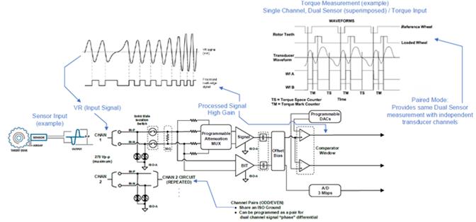
VRS (Variable Reluctance Speed) sensors are designed to detect the speed and position of rotating shafts. These passive VRS sensors are simple, rugged devices that do not require an external voltage source for operation. A permanent magnet in the sensor establishes a fixed magnetic field. The approach and passing of a ferrous metal target near the sensor’s pole piece (sensing area) changes the flux of the magnetic field, dynamically changing its strength. This change in magnetic field strength induces a current into a coil winding which is attached to the output terminals. The output signal of a VRS sensor is an AC voltage that varies in amplitude and frequency as the speed of the monitored device changes and is usually expressed in peak-to-peak voltage (Vp-p). One complete cycle occurs as each tooth passes the sensor’s pole piece.
The signal characteristics of the VR sensor can vary greatly with the speed and proximity of the sensor pickup in relation to the shaft. The VR1 sensor interface is ideal for speed sensing for aircraft, marine or automotive crankshafts, camshafts, brake or gear rotors, transmission shafts, etc. The VR1 provides the measurement basis for linear velocity, angular velocity, and torque. The VR1 interface channels are uniquely designed to compensate for the inherent, typically ‘less-than-ideal’, sensor output signal characteristics. The VR1 integrates a programmable high-gain front end precision amplifier and comparator with adaptive threshold and conditioning circuits that discern and re-define the pulses, even in the presence of substantial system noise or extremely weak VR signals. In paired mode, the conditioned channel pulses, with high slew rates, provide channel-to-channel pulse alignment, eliminating sources of timing error. Paired mode provides the ability to calculate shaft torque by measuring the shaft ‘twist angle’ resulting from the period measurement between the two channel pulses.
The VR1 is also uniquely designed to process signals as general-purpose counter, that can operate and process a wide variety of AC and Pulse input signals as high as ±100 V*. The VR1 is capable of measurements with signal frequencies to 1 MHz (4 MHz is potentially achievable based upon settings e.g. minimal filtering). With auto threshold and auto ranging modes enabled, max operational frequencies to 20 kHz is achievable.
Note
for modules with FPGA rev 1.x, the input voltage range is ±60 V.
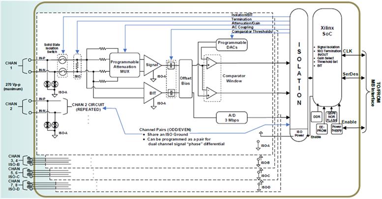
The VR1 provides eight isolated, wide voltage input range Variable Reluctance (VR) signal or general-purpose Pulse Counter measurement interfaces. Channels can be programmed to operate individually or combined in pairs.
Clarifying Terms:
VR (variable reluctance) sensors are known by many other application-specific names. A few examples are:
Magnetic-pickups, Speed sensors, Motion sensors, Pulse generators, Frequency generators, Transducers, Magnetic probes, Timing probes, Monopoles and Pickoffs.
Clarifying Operation Modes:
Monopole sensor type = single sensor pulse train
Dipole sensor type = dual sensor pulse train (can be a single channel interlaced input on Monopole type/mode dual paired channels). Dipoles typically refers to any measurements involving phase (twist, torque), whether in the single channel or dual paired channels modes.
The VR1 can be used for the following signal/pulse measurements:
“Monopole” is defined as the Single Sensor Pulse Train signal type (typically, for measuring RPM, frequency, etc.) - this is defined as a reference term within this document.
“Dipole” will be defined as the Double Pulse signal type (typically, for discerning phase between the double signal pulses for torque/twist measurement) - this is defined as a reference term within this document.
Note
The “Dipole” signal type can be generated (and will be measured) via a single independent composite signal (one signal, with two interlaced sensor inputs)
A dual set of independent signals (two distinct, yet dependent, synchronized signal inputs) where one can manage the measurement with the unique “paired channel mode”.
VR1 Overview
The VR1 module offers a wide range of features designed to suit a variety of system requirements. Some of the key features include:
Variable Reluctance Interface:
-
Eight (8) isolated, differential input channels: These channels provide flexibility in interfacing with various sensor types, ensuring compatibility with the user’s specific application requirements.
-
Independent or paired mode: The VR1 module allows you to configure these input channels independently or in paired mode, enhancing versatility in data acquisition.
-
Large voltage range input: With a range of ±100 V, the VR1 module accommodates a wide range of signal amplitudes, making it suitable for diverse applications.
-
Large pulse train detection: Achieve precise pulse counting with an effective resolution of 8 ns in 1 ns step settings, ensuring accurate data capture even in high-speed scenarios.
General Purpose Counter:
-
32-bit pulse counter: The VR1 boasts a 32-bit counter that enables high-resolution pulse counting.
-
Single channel increment: The VR1 module simplifies pulse counting by incrementing on a single channel, streamlining data acquisition tasks.
-
Frequency: The VR1 module is capable of measurements with signal frequencies up to 1 MHz (maximum, continuous).
Note
Depending on some settings, such as filtering, 4 Mbps is potentially achievable. With auto threshold and auto ranging modes enabled, the frequency limit reaches 20 kHz for a broader range of frequency measurement capabilities.
-
Independent channel configuration: Tailor the VR1 module to interface seamlessly with different sensor types by adjusting programmable parameters. Choose between independent or paired mode configurations to suit your specific application needs.
-
Isolated channels: The VR1 module incorporates isolated channels to minimize the risk of false trigger counts due to electrical noise, ensuring data accuracy.
-
Built-in Test: The VR1 module comes with a built-in test feature, providing assurance of its operational integrity and reliability.
PRINCIPLE OF OPERATION
The VR1 module provides both Variable Reluctance and General-Purpose Counter capability. Programmable parameters allow for this module to be used on many different sensor types. In addition, the VR1 module includes internal built-in tests that provide monitoring of the circuitry.
Variable Reluctance
Variable Reluctance Measurements
The VR1 provides several measurements of the signal characteristics including:
Monopole type/mode:
- Signal Amplitude measured as the absolute value of the maximum positive or negative peak
- Signal Frequency
- Period of the signal
- RPM based on number of teeth on wheel sensor
Dipole type/mode:
- Phase measurement between interposed signal trains (either single or paired channel mode)
Monopole/Dipole
When operating in Dipole mode, the VR1 measures the relative phase between the two Dipole pulses on a single channel, reporting the smaller phase measurement to determine the change in phase from a user reference phase setting. This change is used to calculate the percentage torque reading.
For measurement stability, dipole phase readings crossing through the 0.0/180-degree transitions should be avoided. Optimal configuration is achieved with phase measurements centered about 90 degrees.
When operating in Monopole mode, the VR1 measures the relative phase between pulses on individual channels within channel pairs, reports the phase measurement, and determines the change in phase from a user reference phase setting. This is used for calculation of the percentage torque on a shaft.
For measurement stability, monopole phase readings crossing through the 0.0/360-degree transitions should be avoided. Optimal configuration is achieved with phase measurements centered about 180 degrees.
Sensor Characteristic Compensation
The following sensor signal parameters are programmable to adjust for different sensor type characteristics.
-
Programmable Voltage Range
-
Automatic Gain Control, to adjust amplifier gain, based on measured signal level.
-
Input transition High Threshold
-
Input transition Low Threshold
-
Polarity Select - Measure time from rising or falling edges.
-
AC-coupling Enable
-
Input Termination Enable
-
Measurement Averaging Time
-
Debounce Time
-
Monopole/Dipole Mode
General Purpose Counter
The VR1 can also be used as a general counter for a variety of AC or pulsed signal sensors including Hall effect sensors. Count up mode is presently supported by the module.
Built-In Test
Initiated Built-In Test
The initiated BIT test is initiated by the user, momentarily taking the specified test channels offline for a duration of 1ms. An internal reference signal is measured and verified for accuracy, with the test result displayed in the BIT status register.
Status and Interrupts
The Variable Reluctance and General-Purpose Counter Function Module provide registers that indicate faults or events. Refer to “Status and Interrupts Module Manual” for the Principle of Operation description.
Module Common Registers
The Variable Reluctance and General-Purpose Counter Function Module include module common registers that provide access to module-level bare metal/FPGA revisions & compile times, unique serial number information, and temperature/voltage/current monitoring. Refer to “Module Common Registers Module Manual” for the detailed information.
REGISTER DESCRIPTIONS
The register descriptions provide the register name, Type, Data Range, Read or Write information, Initialized Value, a description of the function and, in most cases, a data table.
VR/Counter Measurement Registers
The measurements of the input signal to the Variable Reluctance/Counter can be read from the registers described in this section.
Measured Period
| Function: | This value is the measured period of the input signal per individual channel. |
| Type: | unsigned binary word (32-bit) (Integer Mode) or Single Precision Floating Point Value (IEEE-754) (Floating Point Mode) |
| Data Range: | (Integer Mode): 0x0000 0000 to 0xFFFF FFFF + (Floating Point Mode): Single Precision Floating Point Value (IEEE-754) |
| Read/Write: | R |
| Initialized Value: | N/A |
| Operational Settings: | Integer Mode: LSB is 1 nanosecond. + Floating Point Mode: Read as a Single Precision Floating Point Value (IEEE-754) where the units are in seconds. |
Measured Phase
| Function: | This value is the phase measurement of a Dipole input signal per individual channel or if the Dipole Enable register is set for Monopole mode, this is the phase measurement with respect to the channel it is paired with (when using Paired Channel Mode) |
|---|---|
| Type: | unsigned binary word (32-bit) (Integer Mode) or Single Precision Floating Point Value (IEEE-754) (Floating Point Mode) |
| Data Range: | (Integer Mode): 0x0000 0000 to 0x0005 7E3F (0 to 359.999º) + (Floating Point Mode): Single Precision Floating Point Value (IEEE-754) |
| Read/Write: | R |
| Initialized Value: | N/A |
| Operational Settings: | Integer Mode: LSB is 0.001°. + Floating Point Mode: Read as a Single Precision Floating Point Value (IEEE-754) where the units are in degrees. |
Measured Percent Torque
| Function: | This value is the percent torque measurement of the input signal per individual channel calculated as follows: Percent Torque = 100 * (Phase Measurement - Zero Torque Signal Phase) / Max Torque Signal Phase |
|---|---|
| Type: | unsigned binary word (32-bit) (Integer Mode) or Single Precision Floating Point Value (IEEE-754) (Floating Point Mode) |
| Data Range: | (Integer Mode): 0x0000 0000 to 0xFFFF FFFF + (Floating Point Mode): Single Precision Floating Point Value (IEEE-754) |
| Read/Write: | R |
| Initialized Value: | N/A |
| Operational Settings: | Integer Mode: LSB is 0.001%. + Floating Point Mode: Read as a Single Precision Floating Point Value (IEEE-754) where the units are in percent. |
Measured Amplitude
| Function: | This value is the absolute value of the maximum positive or negative signal peak amplitude of the input signal per individual channel measured by peak sampling of the input signal. Peak detected values are recorded on an ongoing basis at 1 second intervals. |
|---|---|
| Type: | unsigned binary word (32-bit) (Integer Mode) or Single Precision Floating Point Value (IEEE-754) (Floating Point Mode) |
| Data Range: | (Integer Mode): 0x0000 0000 to 0xFFFF FFFF + (Floating Point Mode): Single Precision Floating Point Value (IEEE-754) |
| Read/Write: | R |
| Initialized Value: | N/A |
| Operational Settings: | Integer Mode: LSB is 1 mV. + Floating Point Mode: Read as a Single Precision Floating Point Value (IEEE-754) in volts. |
Measured Frequency
| Function: | This value is the measured frequency of the input signal per individual channel. NOTE: the frequency readings in dipole mode will be half the apparent frequency as dual-timing references are assumed to be interleaved on the single channel. |
|---|---|
| Type: | unsigned binary word (32-bit) (Integer Mode) or Single Precision Floating Point Value (IEEE-754) (Floating Point Mode) |
| Data Range: | (Integer Mode): 0x0000 0000 to 0xFFFF FFFF + (Floating Point Mode): Single Precision Floating Point Value (IEEE-754) |
| Read/Write: | R |
| Initialized Value: | N/A |
| Operational Settings: | Integer Mode: LSB is 0.001 Hz. + Floating Point Mode: Read as a Single Precision Floating Point Value (IEEE-754) in hertz. |
Measured RPM
| Function: | This value is the measured velocity in RPM (rotations/minute) of the shaft per individual channel. The velocity is based the on Number of Teeth setting for the individual channel. |
|---|---|
| Type: | unsigned binary word (32-bit) (Integer Mode) or Single Precision Floating Point Value (IEEE-754) (Floating Point Mode) |
| Data Range: | (Integer Mode): 0x0000 0000 to 0xFFFF FFFF + (Floating Point Mode): Single Precision Floating Point Value (IEEE-754) |
| Read/Write: | R |
| Initialized Value: | N/A |
| Operational Settings: | Integer Mode: LSB is 0.001 RPM. + Floating Point Mode: Read as a Single Precision Floating Point Value (IEEE-754) in RPM. |
Measured Cycle Count
| Function: | Reads the cycle counter, which counts the number of signal transitions of the channel since it was last reset. The cycle counter will roll over to a ‘0’ count on the next count following a 0xFFFF FFFF terminal count. |
|---|---|
| Type: | unsigned binary word (32-bit) (Integer Mode) or Single Precision Floating Point Value (IEEE-754) (Floating Point Mode) |
| Read/Write: | R |
| Initialized Value: | 0x0000 0000 |
| Data Range: | (Integer Mode): 0x0000 0000 to 0xFFFF FFFF + (Floating Point Mode): Single Precision Floating Point Value (IEEE-754) |
| Operational Settings: | Integer Mode: LSB is 1 cycle. + Floating Point Mode: Read as a Single Precision Floating Point Value (IEEE-754), where 1 = 1 cycle. |
VR/Counter Control Registers
Control of the Variable Reluctance/Counter features are based on the configuration of the registers in this section.
Power Supply Enable
| Function: | Enables the VR1 module. |
|---|---|
| Type: | unsigned binary word (32-bit) |
| Data Range: | 0x0000 0000 to 0x0000 0001 |
| Read/Write: | R/W |
| Initialized Value: | 0x0000 0001 (Channel power is enabled) |
| Operational Settings: | Set bit to 1 to enable the power. Set bit to 0 to disable the power. |
| D31 | D30 | D29 | D28 | D27 | D26 | D25 | D24 | D23 | D22 | D21 | D20 | D19 | D18 | D17 | D16 |
|---|---|---|---|---|---|---|---|---|---|---|---|---|---|---|---|
| 0 | 0 | 0 | 0 | 0 | 0 | 0 | 0 | 0 | 0 | 0 | 0 | 0 | 0 | 0 | 0 |
| D15 | D14 | D13 | D12 | D11 | D10 | D9 | D8 | D7 | D6 | D5 | D4 | D3 | D2 | D1 | D0 |
| 0 | 0 | 0 | 0 | 0 | 0 | 0 | 0 | 0 | 0 | 0 | 0 | 0 | 0 | 0 | D |
Channel Enable
| Function: | Enables the channel. |
|---|---|
| Type: | unsigned binary word (32-bit) |
| Data Range: | 0x0000 0000 to 0x0000 00FF |
| Read/Write: | R/W |
| Initialized Value: | 0x0000 00FF (all channels enabled) |
| Operational Settings: | Set bit to 1 to enable the channel. Set bit to 0 to disable the channel. When both channels of an unused channel pair are disabled, channel operations are suspended for a reduction in power requirements. |
| D31 | D30 | D29 | D28 | D27 | D26 | D25 | D24 | D23 | D22 | D21 | D20 | D19 | D18 | D17 | D16 |
|---|---|---|---|---|---|---|---|---|---|---|---|---|---|---|---|
| 0 | 0 | 0 | 0 | 0 | 0 | 0 | 0 | 0 | 0 | 0 | 0 | 0 | 0 | 0 | 0 |
| D15 | D14 | D13 | D12 | D11 | D10 | D9 | D8 | D7 | D6 | D5 | D4 | D3 | D2 | D1 | D0 |
| 0 | 0 | 0 | 0 | 0 | 0 | 0 | 0 | Ch8 | Ch7 | Ch6 | Ch5 | Ch4 | Ch3 | Ch2 | Ch1 |
Dipole Enable
| Function: | Enables a single channel to be used for reading a dipole VR sensor. |
|---|---|
| Type: | unsigned binary word (32-bit) |
| Data Range: | 0x0000 0000 to 0x0000 00FF |
| Read/Write: | R/W |
| Initialized Value: | 0x0000 0000 (default is considered “paired channel mode” or “combined signal disabled”) |
| Operational Settings: | Sets what type of sensor is being interfaced to, where 0 = Monopole and 1 = Dipole. In default Monopole mode (Dipole Enable = 0), the channel 1’s phase is measured with respect to channel 2 (a.k.a Paired Mode). Channels are paired in groups of two. Pairs are (1,2) (3,4) (5,6) (7,8). Setting this bit (Dipole Enable = 1) makes the channel independent of its paired channel and assumes that both signals are combined on the selected channel. |
| D31 | D30 | D29 | D28 | D27 | D26 | D25 | D24 | D23 | D22 | D21 | D20 | D19 | D18 | D17 | D16 |
|---|---|---|---|---|---|---|---|---|---|---|---|---|---|---|---|
| 0 | 0 | 0 | 0 | 0 | 0 | 0 | 0 | 0 | 0 | 0 | 0 | 0 | 0 | 0 | 0 |
| D15 | D14 | D13 | D12 | D11 | D10 | D9 | D8 | D7 | D6 | D5 | D4 | D3 | D2 | D1 | D0 |
| 0 | 0 | 0 | 0 | 0 | 0 | 0 | 0 | Ch8 | Ch7 | Ch6 | Ch5 | Ch4 | Ch3 | Ch2 | Ch1 |
Falling Edge Measurement Enable
| Function: | Sets the signal edge on which to take measurements on the channel. |
|---|---|
| Type: | unsigned binary word (32-bit) |
| Data Range: | 0x0000 0000 to 0x0000 00FF |
| Read/Write: | R/W |
| Initialized Value: | 0x0000 0000 (rising edge) |
| Operational Settings: | Set bit to 1 to measure on falling edge for that channel. Set bit to 0 to measure on rising edge. |
| D31 | D30 | D29 | D28 | D27 | D26 | D25 | D24 | D23 | D22 | D21 | D20 | D19 | D18 | D17 | D16 |
|---|---|---|---|---|---|---|---|---|---|---|---|---|---|---|---|
| 0 | 0 | 0 | 0 | 0 | 0 | 0 | 0 | 0 | 0 | 0 | 0 | 0 | 0 | 0 | 0 |
| D15 | D14 | D13 | D12 | D11 | D10 | D9 | D8 | D7 | D6 | D5 | D4 | D3 | D2 | D1 | D0 |
| 0 | 0 | 0 | 0 | 0 | 0 | 0 | 0 | Ch8 | Ch7 | Ch6 | Ch5 | Ch4 | Ch3 | Ch2 | Ch1 |
Termination Enable
| Function: | Enables Termination on the channel. |
|---|---|
| Type: | unsigned binary word (32-bit) |
| Data Range: | 0x0000 0000 to 0x0000 00FF |
| Read/Write: | R/W |
| Initialized Value: | 0x0000 0000 (all channels unterminated) |
| Operational Settings: Set bit to 1 to enable a 50Ω (nominal) termination on the channel. Set bit to 0 for high impedance channel input. |
| D31 | D30 | D29 | D28 | D27 | D26 | D25 | D24 | D23 | D22 | D21 | D20 | D19 | D18 | D17 | D16 |
|---|---|---|---|---|---|---|---|---|---|---|---|---|---|---|---|
| 0 | 0 | 0 | 0 | 0 | 0 | 0 | 0 | 0 | 0 | 0 | 0 | 0 | 0 | 0 | 0 |
| D15 | D14 | D13 | D12 | D11 | D10 | D9 | D8 | D7 | D6 | D5 | D4 | D3 | D2 | D1 | D0 |
| 0 | 0 | 0 | 0 | 0 | 0 | 0 | 0 | Ch8 | Ch7 | Ch6 | Ch5 | Ch4 | Ch3 | Ch2 | Ch1 |
AC Couple Enable
| Function: | Enables AC Coupling on the channel. |
|---|---|
| Type: | unsigned binary word (32-bit) |
| Data Range: | 0x0000 0000 to 0x0000 00FF |
| Read/Write: | R/W |
| Initialized Value: | 0x0000 0000 (all channels DC coupled) |
| Operational Settings: | Set bit to 1 to enable AC coupling on the channel. Set bit to 0 for DC coupling. |
| D31 | D30 | D29 | D28 | D27 | D26 | D25 | D24 | D23 | D22 | D21 | D20 | D19 | D18 | D17 | D16 |
|---|---|---|---|---|---|---|---|---|---|---|---|---|---|---|---|
| 0 | 0 | 0 | 0 | 0 | 0 | 0 | 0 | 0 | 0 | 0 | 0 | 0 | 0 | 0 | 0 |
| D15 | D14 | D13 | D12 | D11 | D10 | D9 | D8 | D7 | D6 | D5 | D4 | D3 | D2 | D1 | D0 |
| 0 | 0 | 0 | 0 | 0 | 0 | 0 | 0 | Ch8 | Ch7 | Ch6 | Ch5 | Ch4 | Ch3 | Ch2 | Ch1 |
Range Select
| Function: | Selects the signal gain, which sets the effective measuring range on the channel. |
|---|---|
| Type: | unsigned binary word (32-bit) |
| Data Range: | 0x0000 0000 to 0xFFFF FFFF |
| Read/Write: | R/W |
| Initialized Value: | 0x0000 0000 (auto range) |
| Operational Settings: | Set 4-bit groups to select the signal gain for the specified channel. e.g. 0xAA0 will set channels 2 and 3 to 50V range. Set bit group to 0 for auto ranging. |
| D31 | D30 | D29 | D28 | D27 | D26 | D25 | D24 | D23 | D22 | D21 | D20 | D19 | D18 | D17 | D16 |
|---|---|---|---|---|---|---|---|---|---|---|---|---|---|---|---|
| Ch8 | Ch8 | Ch8 | Ch8 | Ch7 | Ch7 | Ch7 | Ch7 | Ch6 | Ch6 | Ch6 | Ch6 | Ch5 | Ch5 | Ch5 | Ch5 |
| D15 | D14 | D13 | D12 | D11 | D10 | D9 | D8 | D7 | D6 | D5 | D4 | D3 | D2 | D1 | D0 |
| Ch4 | Ch4 | Ch4 | Ch4 | Ch3 | Ch3 | Ch3 | Ch3 | Ch2 | Ch2 | Ch2 | Ch2 | Ch1 | Ch1 | Ch1 | Ch1 |
| Channel Value | Range |
|---|---|
| 0x0 | Auto Range |
| 0x1 | ±50mV |
| 0x2 | ±100mV |
| 0x3 | ±250mV |
| 0x4 | ±500mV |
| 0x5 | ±1V |
| 0x6 | ±2.5V |
| 0x7 | ±5V |
| 0x8 | ±12.5V |
| 0x9 | ±25V |
| 0xA | ±50V |
| 0xB | ±100V |
Auto Down-Range Time
| Function: | Sets the amount of time for the auto-ranging detection to down-range (increase the gain). |
|---|---|
| Type: | unsigned binary word (32-bit) |
| Data Range: | 0x0000 0000 to 0xFFFF FFFF |
| Read/Write: | R/W |
| Initialized Value: | 0x2 (1s) |
| Operational Settings: Upward range changes in response to peaks exceeding 90% of current range will take effect immediately and will not be delayed by this selection. Downward range changes in response to troughs below 40% of the next lower range (delayed by auto down-range time setting). |
| D31 | D30 | D29 | D28 | D27 | D26 | D25 | D24 | D23 | D22 | D21 | D20 | D19 | D18 | D17 | D16 |
|---|---|---|---|---|---|---|---|---|---|---|---|---|---|---|---|
| 0 | 0 | 0 | 0 | 0 | 0 | 0 | 0 | 0 | 0 | 0 | 0 | 0 | 0 | 0 | 0 |
| D15 | D14 | D13 | D12 | D11 | D10 | D9 | D8 | D7 | D6 | D5 | D4 | D3 | D2 | D1 | D0 |
| 0 | 0 | 0 | 0 | 0 | 0 | 0 | 0 | Ch8 | Ch7 | Ch6 | Ch5 | Ch4 | Ch3 | Ch2 | Ch1 |
| Channel Value | Range |
|---|---|
| 0x0 | 100 ms |
| 0x1 | 500 ms |
| 0x2 | 1 s |
| 0x3 | 2 s |
| 0x4 | 5 s |
| 0x5 | 10 s |
Number of Teeth
| Function: | Sets the number of teeth on the reluctor ring, which is used for RPM calculations. |
|---|---|
| Type: | unsigned binary word (32-bit) (Integer Mode) or Single Precision Floating Point Value (IEEE-754) (Floating Point Mode) |
| Data Range: | (Integer Mode): 0x0000 0000 to 0xFFFF FFFF (Floating Point Mode): Single Precision Floating Point Value (IEEE-754) Integer Mode: LSB is 1 tooth. Floating Point Mode: Read as a Single Precision Floating Point Value (IEEE-754), where 1 = 1 tooth. |
| Read/Write: | R/W |
| Initialized Value: | 0x0000 0001 |
| Operational Settings: | Sets the number of teeth for the channel. |
Zero Torque Signal Phase
| Function: | Sets the zero-torque signal phase value to use for torque calculations of the channel. |
|---|---|
| Type: | unsigned binary word (32-bit) (Integer Mode) or Single Precision Floating Point Value (IEEE-754) (Floating Point Mode) |
| Data Range: | (Integer Mode): 0x0000 0000 to 0xFFFF FFFF (Floating Point Mode): Single Precision Floating Point Value (IEEE-754) Integer Mode: LSB is .001°. Floating Point Mode: Read as a Single Precision Floating Point Value (IEEE-754), where 1 = 1°. |
| Read/Write: | R/W |
| Initialized Value: | 0x0000 0000 (0°) |
| Operational Settings: | Sets the zero-torque signal reference used for torque calculations. This register can be also set automatically by strobing the set zero torque signal phase register, to transfer the current reading and null the torque value. |
Zero Torque Signal Phase to Phase Reading
| Function: | Sets the current phase as the zero-torque signal phase value for the channels. |
|---|---|
| Type: | unsigned binary word (32-bit) |
| Data Range: | 0x0000 0000 to 0x0000 00FF Read/Write: |
| Read/Write: | W (always reads 0x0000 0000) |
| Initialized Value: | 0x0000 0000 |
| Operational Settings: | Set bit to 1 to transfer the present phase readings to the zero-torque signal phase settings for the specified channels. This allows for nulling of the torque reading to zero for the present conditions. |
| D31 | D30 | D29 | D28 | D27 | D26 | D25 | D24 | D23 | D22 | D21 | D20 | D19 | D18 | D17 | D16 |
|---|---|---|---|---|---|---|---|---|---|---|---|---|---|---|---|
| 0 | 0 | 0 | 0 | 0 | 0 | 0 | 0 | 0 | 0 | 0 | 0 | 0 | 0 | 0 | 0 |
| D15 | D14 | D13 | D12 | D11 | D10 | D9 | D8 | D7 | D6 | D5 | D4 | D3 | D2 | D1 | D0 |
| 0 | 0 | 0 | 0 | 0 | 0 | 0 | 0 | Ch8 | Ch7 | Ch6 | Ch5 | Ch4 | Ch3 | Ch2 | Ch1 |
Max Torque Signal Phase
| Function: | Sets the max torque signal phase value to use for torque calculations for the channel. This is a scaling value that represents the amount of change in the phase measurement from the Zero Torque Signal Phase reference setting for 100% torque. |
|---|---|
| Type: | unsigned binary word (32-bit) (Integer Mode) or Single Precision Floating Point Value (IEEE-754) (Floating Point Mode) |
| Data Range: | (Integer Mode): 0x0000 0000 to 0xFFFF FFFF (Floating Point Mode): Single Precision Floating Point Value (IEEE-754) Integer Mode: LSB is .001°. Floating Point Mode: Read as a Single Precision Floating Point Value (IEEE-754), where 1 = 1°. |
| Read/Write: | R/W |
| Initialized Value: | 0x0000 03E8 (1°) |
| Operational Settings: | Sets the max torque signal value to use for torque calculations for the channel. |
Averaging Time
| Function: | Sets the averaging time for all readings of the channel. |
|---|---|
| Type: | unsigned binary word (32-bit) (Integer Mode) or Single Precision Floating Point Value (IEEE-754) (Floating Point Mode) |
| Data Range: | 0x0000 0000 to 0xFFFF FFFF |
| Read/Write: | R/W |
| Initialized Value: | 0x0000 0000 (no averaging) |
| Operational Settings: | Sets the averaging time for the channel. Higher averaging times provide improved accuracy and measurement stability, with longer update rates. |
| Data Range: | (Integer Mode): 0x0000 0000 to 0xFFFF FFFF (Floating Point Mode): Single Precision Floating Point Value (IEEE-754) Integer Mode: LSB is 1us. Floating Point Mode: Read as a Single Precision Floating Point Value (IEEE-754), where 1 = 1 second. |
Debounce Time
| Function: | Sets the debounce time for all readings of the channel. |
|---|---|
| Type: | unsigned binary word (32-bit) (Integer Mode) or Single Precision Floating Point Value (IEEE-754) (Floating Point Mode) |
| Data Range: | (Integer Mode): 0x0000 0000 to 0xFFFF FFFF (Floating Point Mode): Single Precision Floating Point Value (IEEE-754) Integer Mode: LSB is 1ns, with effective debounce gradations of 8ns implemented. Floating Point Mode: Read as a Single Precision Floating Point Value (IEEE-754), where 1 = 1 second. |
| Read/Write: | R/W |
| Initialized Value: | 0x0000 0000 (no debounce) |
| Operational Settings: | Sets the debounce time for the channel, to reject spurious noise transitions. |
Voltage Threshold High
| Function: | Sets the high threshold voltage, used in the input comparator of the channel. |
|---|---|
| Type: | 2’s compliment (Integer Mode) or Single Precision Floating Point Value (IEEE-754) (Floating Point Mode) |
| Data Range: | (Integer Mode): 0x0000 0000 to 0x0001 7318 (Floating Point Mode): Single Precision Floating Point Value (IEEE-754) Integer Mode: LSB is 1mV. Floating Point Mode: Read as a Single Precision Floating Point Value (IEEE-754), where 1 = 1V. |
| Read/Write: | R/W |
| Initialized Value: | 0x0000 0000 (0V) |
| Operational Settings: | Sets the high threshold trigger voltage for the channel. The operational range should be limited to +95V. |
Voltage Threshold Low
| Function: | Sets the low threshold voltage, used for the input comparator of the channel. |
|---|---|
| Type: | 2’s compliment (Integer Mode) or Single Precision Floating Point Value (IEEE-754) (Floating Point Mode) |
| Data Range: | (Integer Mode): 0xFFFE 8CE8 to 0xFFFF FFFF (Floating Point Mode): Single Precision Floating Point Value (IEEE-754) Integer Mode: LSB is 1mV. Floating Point Mode: Read as a Single Precision Floating Point Value (IEEE-754), where 1 = 1V. |
| Read/Write: | R/W |
| Initialized Value: | 0x0000 0000 (0V) |
| Operational Settings: | Sets the Voltage Threshold Low for the channel. The operational range should be limited to -95V. |
Minimum Amplitude
| Function: | Sets the minimum amplitude threshold for triggering a signal loss status on the channel. |
|---|---|
| Type: | unsigned binary word (32-bit) (Integer Mode) or Single Precision Floating Point Value (IEEE-754) (Floating Point Mode) |
| Data Range: | (Integer Mode): 0x0000 0000 to 0xFFFF FFFF (Floating Point Mode): Single Precision Floating Point Value (IEEE-754) Integer Mode: LSB is 1mV. Floating Point Mode: Read as a Single Precision Floating Point Value (IEEE-754), where 1 = 1V. |
| Read/Write: | R/W |
| Initialized Value: | 0x0000 0000 (0V) |
| Operational Settings: | Sets the Minimum Amplitude for the channel. Suggested operational range is 0V to 100V. |
Minimum Frequency
| Function: | Sets the minimum frequency threshold for triggering a signal loss status on the channel. |
|---|---|
| Type: | unsigned binary word (32-bit) (Integer Mode) or Single Precision Floating Point Value (IEEE-754) (Floating Point Mode) |
| Data Range: | (Integer Mode): 0x0000 0000 to 0xFFFF FFFF (Floating Point Mode): Single Precision Floating Point Value (IEEE-754) Integer Mode: LSB is .001Hz. Floating Point Mode: Read as a Single Precision Floating Point Value (IEEE-754), where 1 = 1Hz. |
| Read/Write: | R/W |
| Initialized Value: | 0x0000 00FA (.25Hz) |
| Operational Settings: | Sets the Minimum Frequency for the channel. |
Reset Cycle Count
| Function: | Resets the cycle count value for the channel. |
|---|---|
| Type: | unsigned binary word (32-bit) |
| Data Range: | 0x0000 0000 to 0x0000 00FF |
| Read/Write: | W (always reads 0x0000 0000) |
| Initialized Value: | 0x0000 0000 |
| Operational Settings: | Set bit to 1 to reset the cycle count value for the specified channels. |
| D31 | D30 | D29 | D28 | D27 | D26 | D25 | D24 | D23 | D22 | D21 | D20 | D19 | D18 | D17 | D16 |
|---|---|---|---|---|---|---|---|---|---|---|---|---|---|---|---|
| 0 | 0 | 0 | 0 | 0 | 0 | 0 | 0 | 0 | 0 | 0 | 0 | 0 | 0 | 0 | 0 |
| D15 | D14 | D13 | D12 | D11 | D10 | D9 | D8 | D7 | D6 | D5 | D4 | D3 | D2 | D1 | D0 |
| 0 | 0 | 0 | 0 | 0 | 0 | 0 | 0 | Ch8 | Ch7 | Ch6 | Ch5 | Ch4 | Ch3 | Ch2 | Ch1 |
Auto Threshold Percent
| Function: | Sets the percent of peak amplitude to set the active edge threshold in auto threshold mode of the channel. |
|---|---|
| Type: | 2’s compliment (Integer Mode) or Single Precision Floating Point Value (IEEE-754) (Floating Point Mode) |
| Data Range: | (Integer Mode): 0x0000 0000 to 0x0001 86A0 (Floating Point Mode): Single Precision Floating Point Value (IEEE-754) Integer Mode: LSB is .001%. Floating Point Mode: Read as a Single Precision Floating Point Value (IEEE-754), where 1 = 1%. |
| Read/Write: | R/W |
| Initialized Value: | 0x0000 0000 (0%) |
| Operational Settings: | Sets the percent of peak amplitude to set the active edge threshold in auto threshold mode of the channel. The maximum value is 100% (0x186A0). |
Auto Threshold Hysteresis
| Function: | Sets the percentage of hysteresis to set the opposite edge threshold in auto threshold mode of the channel. |
|---|---|
| Type: | 2’s compliment (Integer Mode) or Single Precision Floating Point Value (IEEE-754) (Floating Point Mode) |
| Data Range: | (Integer Mode): 0x0000 0000 to 0x0001 86A0 (Floating Point Mode): Single Precision Floating Point Value (IEEE-754) Integer Mode: LSB is .001%. Floating Point Mode: Read as a Single Precision Floating Point Value (IEEE-754), where 1 = 1%. |
| Read/Write: | R/W |
| Initialized Value: | 0x0000 0000 (0%) |
| Operational Settings: | Sets the Auto Threshold Hysteresis for the channel. The opposite edge threshold is used to reset the trigger detection circuit. Larger values afford greater immunity from multiple trigger events due to noise but should be set low enough for proper response with low signal amplitudes. The maximum value is 100% (0x186A0). |
Auto Threshold Enable
| Function: | Enables automatic threshold levels for the channel. |
|---|---|
| Type: | unsigned binary word (32-bit) |
| Data Range: | 0x0000 0000 to 0x0000 00FF |
| Read/Write: | R/W |
| Initialized Value: | 0x0000 0000 (disabled) |
| Operational Settings: | Set bit to 1 to enable auto threshold for the channel and automatically set input gain range based on the detected signal. |
| D31 | D30 | D29 | D28 | D27 | D26 | D25 | D24 | D23 | D22 | D21 | D20 | D19 | D18 | D17 | D16 |
|---|---|---|---|---|---|---|---|---|---|---|---|---|---|---|---|
| 0 | 0 | 0 | 0 | 0 | 0 | 0 | 0 | 0 | 0 | 0 | 0 | 0 | 0 | 0 | 0 |
| D15 | D14 | D13 | D12 | D11 | D10 | D9 | D8 | D7 | D6 | D5 | D4 | D3 | D2 | D1 | D0 |
| 0 | 0 | 0 | 0 | 0 | 0 | 0 | 0 | Ch8 | Ch7 | Ch6 | Ch5 | Ch4 | Ch3 | Ch2 | Ch1 |
Unit Conversion Programming Registers
The Enable Floating Point register provides the ability to read the measurement registers as floating-point values. The purpose for this feature is to offload the processing that is normally performed by the mission processor to convert the integer values to floating-point values.
Enable Floating Point Mode
| Function: | Sets all channels for floating point mode or integer module. |
|---|---|
| Type: | unsigned binary word (32-bit) |
| Data Range: | 0 to 1 |
| Read/Write: | R/W |
| Initialized Value: | 0 |
| Operational Settings: Set bit to 1 to enable Floating Point Mode and 0 for Integer Mode. Wait for the Floating Point State register to match the value for the requested Floating Point Mode (Integer = 0, Floating Point = 1); this indicates that the module’s conversion of the register values and internal values is complete before changing the values of the configuration and control registers with the values in the units specified (Integer or Floating Point). |
| D31 | D30 | D29 | D28 | D27 | D26 | D25 | D24 | D23 | D22 | D21 | D20 | D19 | D18 | D17 | D16 |
|---|---|---|---|---|---|---|---|---|---|---|---|---|---|---|---|
| 0 | 0 | 0 | 0 | 0 | 0 | 0 | 0 | 0 | 0 | 0 | 0 | 0 | 0 | 0 | 0 |
| D15 | D14 | D13 | D12 | D11 | D10 | D9 | D8 | D7 | D6 | D5 | D4 | D3 | D2 | D1 | D0 |
| 0 | 0 | 0 | 0 | 0 | 0 | 0 | 0 | D | D | D | D | D | D | D | D |
Floating Point State
| Function: | Indicates the state of the mode selected (Integer or Floating Point). |
|---|---|
| Type: | unsigned binary word (32-bit) |
| Data Range: | 0 to 1 |
| Read/Write: | R |
| Initialized Value: | 0 |
| Operational Settings: | Indicates the whether the module registers are in Integer (0) or Floating Point Mode (1). When the Enable Floating Point Mode is modified, the application must wait until this register’s value matches the requested mode before changing the values of the configuration and control registers with the values in the units specified (Integer or Floating Point). |
| D31 | D30 | D29 | D28 | D27 | D26 | D25 | D24 | D23 | D22 | D21 | D20 | D19 | D18 | D17 | D16 |
|---|---|---|---|---|---|---|---|---|---|---|---|---|---|---|---|
| 0 | 0 | 0 | 0 | 0 | 0 | 0 | 0 | 0 | 0 | 0 | 0 | 0 | 0 | 0 | 0 |
| D15 | D14 | D13 | D12 | D11 | D10 | D9 | D8 | D7 | D6 | D5 | D4 | D3 | D2 | D1 | D0 |
| 0 | 0 | 0 | 0 | 0 | 0 | 0 | 0 | 0 | 0 | 0 | 0 | 0 | 0 | 0 | D |
Test Registers
The Variable Reluctance module provides the ability to run an initiated test (IBIT).
Test Enable
| Function: | Set bit IBIT to enable the associated Initiated Built-In-Test. |
|---|---|
| Type: | unsigned binary word (32-bit) |
| Data Range: | 0 to 0x0000 0008 |
| Read/Write: | R/W |
| Initialized Value: | 0x0 |
| Operational Settings: | Command strobe for Initiated BIT test. Writing 0x8 to set bit D3 in the register will initiate an internal test on all enabled channels, taking approximately 1 ms to complete. Channel operations will be offline during the test. The register will read back 0 upon completion. Failures in the BIT test are reflected in the BIT Status registers for non-compliant channels. |
| D31 | D30 | D29 | D28 | D27 | D26 | D25 | D24 | D23 | D22 | D21 | D20 | D19 | D18 | D17 | D16 |
|---|---|---|---|---|---|---|---|---|---|---|---|---|---|---|---|
| 0 | 0 | 0 | 0 | 0 | 0 | 0 | 0 | 0 | 0 | 0 | 0 | 0 | 0 | 0 | 0 |
| D15 | D14 | D13 | D12 | D11 | D10 | D9 | D8 | D7 | D6 | D5 | D4 | D3 | D2 | D1 | D0 |
| 0 | 0 | 0 | 0 | 0 | 0 | 0 | 0 | 0 | 0 | 0 | 0 | IBIT | 0 | 0 | 0 |
Module Common Registers
Refer to “Module Common Registers Module Manual” for the register descriptions.
Status and Interrupt Registers
The VR1 Module provides status registers for BIT, Termination Fault, Signal Loss and Summary Status.
Channel Status Enabled
| Function: | Determines whether to update the status for the channels. This feature can be used to “mask” status bits of unused channels in status registers that are bitmapped by channel. |
|---|---|
| Type: | unsigned binary word (32-bit) |
| Data Range: | 0x0000 0000 to 0x0000 00FF (Channel Status) |
| Read/Write: | R/W |
| Initialized Value: | 0x0000 00FF |
| Operational Settings: | When the bit corresponding to a given channel in the Channel Status Enabled register is not enabled (0) the status will be masked and report “0” or “no failure”. This applies to all statuses that are bitmapped by channel (BIT Status, Termination Fault Status and Summary Status). |
| D31 | D30 | D29 | D28 | D27 | D26 | D25 | D24 | D23 | D22 | D21 | D20 | D19 | D18 | D17 | D16 |
|---|---|---|---|---|---|---|---|---|---|---|---|---|---|---|---|
| 0 | 0 | 0 | 0 | 0 | 0 | 0 | 0 | 0 | 0 | 0 | 0 | 0 | 0 | 0 | 0 |
| D15 | D14 | D13 | D12 | D11 | D10 | D9 | D8 | D7 | D6 | D5 | D4 | D3 | D2 | D1 | D0 |
| 0 | 0 | 0 | 0 | 0 | 0 | 0 | 0 | Ch8 | Ch7 | Ch6 | Ch5 | Ch4 | Ch3 | Ch2 | Ch1 |
BIT Status
There are four registers associated with the BIT Status: Dynamic Status, Latched Status, Interrupt Enable, and Set Edge/Level Interrupt.
| Function: | Sets the corresponding bit associated with the channel’s BIT error. |
|---|---|
| Type: | unsigned binary word (32-bits) |
| Data Range: | 0x0000 0000 to 0x0000 00FF |
| Read/Write: | R (Dynamic), R/W (Latched, Interrupt Enable, Edge/Level Interrupt) |
| Initialized Value: | 0 |
| BIT Set Edge/Level Interrupt | |||||||||||||||
| BIT Interrupt Enable | |||||||||||||||
| BIT Latched Status | |||||||||||||||
| BIT Dynamic Status | |||||||||||||||
| D31 | D30 | D29 | D28 | D27 | D26 | D25 | D24 | D23 | D22 | D21 | D20 | D19 | D18 | D17 | D16 |
| 0 | 0 | 0 | 0 | 0 | 0 | 0 | 0 | 0 | 0 | 0 | 0 | 0 | 0 | 0 | 0 |
| D15 | D14 | D13 | D12 | D11 | D10 | D9 | D8 | D7 | D6 | D5 | D4 | D3 | D2 | D1 | D0 |
| 0 | 0 | 0 | 0 | 0 | 0 | 0 | 0 | Ch8 | Ch7 | Ch6 | Ch5 | Ch4 | Ch3 | Ch2 | Ch1 |
Termination Fault Status
There are four registers associated with the Termination Fault Status: Dynamic Status, Latched Status, Interrupt Enable, and Set Edge/Level Interrupt.
| Function: | Status for termination fault. If the input voltage exceeds 5 volts while termination is enabled, the bit associated with that channel will be set to a 1. |
|---|---|
| Type: | unsigned binary word (32-bits) |
| Data Range: | 0x0000 0000 to 0x0000 00FF |
| Read/Write: | R (Dynamic), R/W (Latched, Interrupt Enable, Edge/Level Interrupt) |
| Initialized Value: | 0x00000000 |
| Termination Fault Set Edge/Level Interrupt | |||||||||||||||
| Termination Fault Interrupt Enable | |||||||||||||||
| Termination Fault Latched Status | |||||||||||||||
| Termination Fault Dynamic Status | |||||||||||||||
| D31 | D30 | D29 | D28 | D27 | D26 | D25 | D24 | D23 | D22 | D21 | D20 | D19 | D18 | D17 | D16 |
| 0 | 0 | 0 | 0 | 0 | 0 | 0 | 0 | 0 | 0 | 0 | 0 | 0 | 0 | 0 | 0 |
| D15 | D14 | D13 | D12 | D11 | D10 | D9 | D8 | D7 | D6 | D5 | D4 | D3 | D2 | D1 | D0 |
| 0 | 0 | 0 | 0 | 0 | 0 | 0 | 0 | Ch8 | Ch7 | Ch6 | Ch5 | Ch4 | Ch3 | Ch2 | Ch1 |
Signal Loss Status
There are four registers associated with the Signal Loss Status: Dynamic Status, Latched Status, Interrupt Enable, and Set Edge/Level Interrupt.
| Function: | Status for termination fault. If the input voltage exceeds 5 volts while termination is enabled, the bit associated with that channel will be set to a 1. |
|---|---|
| Type: | unsigned binary word (32-bits) |
| Data Range: | 0x0000 0000 to 0x0000 00FF |
| Read/Write: | R (Dynamic), R/W (Latched, Interrupt Enable, Edge/Level Interrupt) |
| Initialized Value: | 0x00000000 |
| Signal Loss Set Edge/Level Interrupt | |||||||||||||||
| Signal Loss Interrupt Enable | |||||||||||||||
| Signal Loss Latched Status | |||||||||||||||
| Signal Loss Dynamic Status | |||||||||||||||
| D31 | D30 | D29 | D28 | D27 | D26 | D25 | D24 | D23 | D22 | D21 | D20 | D19 | D18 | D17 | D16 |
| 0 | 0 | 0 | 0 | 0 | 0 | 0 | 0 | 0 | 0 | 0 | 0 | 0 | 0 | 0 | 0 |
| D15 | D14 | D13 | D12 | D11 | D10 | D9 | D8 | D7 | D6 | D5 | D4 | D3 | D2 | D1 | D0 |
| 0 | 0 | 0 | 0 | 0 | 0 | 0 | 0 | Ch8 | Ch7 | Ch6 | Ch5 | Ch4 | Ch3 | Ch2 | Ch1 |
Summary Status
There are four registers associated with the Summary Status: Dynamic Status, Latched Status, Interrupt Enable, and Set Edge/Level Interrupt.
| Function: | Sets the corresponding bit associated with the channel that has an error condition - BIT, Termination Fault or Signal Loss. |
|---|---|
| Type: | unsigned binary word (32-bits) |
| Data Range: | 0x0000 0000 to 0x0000 00FF |
| Read/Write: | R (Dynamic), R/W (Latched, Interrupt Enable, Set Edge/Level Interrupt) |
| Initialized Value: | NA |
| Summary Set Edge/Level Interrupt | |||||||||||||||
| Summary Interrupt Enable | |||||||||||||||
| Summary Latched Status | |||||||||||||||
| Summary Dynamic Status | |||||||||||||||
| D31 | D30 | D29 | D28 | D27 | D26 | D25 | D24 | D23 | D22 | D21 | D20 | D19 | D18 | D17 | D16 |
| 0 | 0 | 0 | 0 | 0 | 0 | 0 | 0 | 0 | 0 | 0 | 0 | 0 | 0 | 0 | 0 |
| D15 | D14 | D13 | D12 | D11 | D10 | D9 | D8 | D7 | D6 | D5 | D4 | D3 | D2 | D1 | D0 |
| 0 | 0 | 0 | 0 | 0 | 0 | 0 | 0 | Ch8 | Ch7 | Ch6 | Ch5 | Ch4 | Ch3 | Ch2 | Ch1 |
Interrupt Vector and Summary
When interrupts are enabled, the interrupt vector associated with the specific interrupt can be programmed (typically with a unique number/identifier) such that it can be utilized in the Interrupt Service Routine (ISR) to identify the type of interrupt. When an interrupt occurs, the contents of the Interrupt Vector register is reported as part of the interrupt mechanism.
In addition to specifying the interrupt vector, the interrupt can be directed (“steered”) to the native bus or to the application running on the onboard ARM processor.
Note
The Interrupt Vector and Interrupt Steering registers are mapped to the Motherboard Common Memory and these registers are associated with the Module Slot position (refer to Function Register Map).
Interrupt Vector
| Function: | Set an identifier for the interrupt. Type: unsigned binary word (32-bit) |
|---|---|
| Type: | unsigned binary word (32-bit) |
| Read/Write: | R/W |
| Initialized Value: | 0 |
| Operational Settings: | When an interrupt occurs, this value is reported as part of the interrupt mechanism. |
Interrupt Steering
| Function: | Sets where to direct the interrupt. Type: unsigned binary word (32-bit) |
|---|---|
| Type: | unsigned binary word (32-bit) |
| Read/Write: | R/W |
| Initialized Value: | 0 |
| Operational Settings: | When an interrupt occurs, the interrupt is sent as specified: |
| Direct Interrupt to VME | 1 |
|---|---|
| Direct Interrupt to ARM Processor (via SerDes) (Custom App on ARM or NAI Ethernet Listener App) | 2 |
| Direct Interrupt to PCIe Bus | 5 |
| Direct Interrupt to cPCI Bus | 6 |
FUNCTION REGISTER MAP
Key:
| Bold Italic | = Configuration/Control |
|---|---|
| Bold Underline | = Status |
*When an event is detected, the bit associated with the event is set in this register and will remain set until the user clears the event bit. Clearing the bit requires writing a 1 back to the specific bit that was set when read (i.e., write-1-to-clear, writing a “1” to a bit set to “1” will set the bit to “0).
~ Data is always in Floating Point
VR/Counter Measurement Registers
| Addr (Hex) | Name | Read/Write |
|---|---|---|
| 0x2010 | Measured Period Ch 1 | R |
| 0x2110 | Measured Period Ch 2 | R |
| 0x2210 | Measured Period Ch 3 | R |
| 0x2310 | Measured Period Ch 4 | R |
| 0x2410 | Measured Period Ch 5 | R |
| 0x2510 | Measured Period Ch 6 | R |
| 0x2610 | Measured Period Ch 7 | R |
| 0x2710 | Measured Period Ch 8 | R |
| Addr (Hex) | Name | Read/Write |
|---|---|---|
| 0x2014 | Measured Phase Ch 1 | R |
| 0x2114 | Measured Phase Ch 2 | R |
| 0x2214 | Measured Phase Ch 3 | R |
| 0x2314 | Measured Phase Ch 4 | R |
| 0x2414 | Measured Phase Ch 5 | R |
| 0x2514 | Measured Phase Ch 6 | R |
| 0x2614 | Measured Phase Ch 7 | R |
| 0x2714 | Measured Phase Ch 8 | R |
| Addr (Hex) | Name | Read/Write |
|---|---|---|
| 0x2018 | Measured Percent Torque Ch 1 | R |
| 0x2118 | Measured Percent Torque Ch 2 | R |
| 0x2218 | Measured Percent Torque Ch 3 | R |
| 0x2318 | Measured Percent Torque Ch 4 | R |
| 0x2418 | Measured Percent Torque Ch 5 | R |
| 0x2518 | Measured Percent Torque Ch 6 | R |
| 0x2618 | Measured Percent Torque Ch 7 | R |
| 0x2718 | Measured Percent Torque Ch 8 | R |
| Addr (Hex) | Name | Read/Write |
|---|---|---|
| 0x201C | Measured Amplitude Ch 1 | R |
| 0x211C | Measured Amplitude Ch 2 | R |
| 0x221C | Measured Amplitude Ch 3 | R |
| 0x231C | Measured Amplitude Ch 4 | R |
| 0x241C | Measured Amplitude Ch 5 | R |
| 0x251C | Measured Amplitude Ch 6 | R |
| 0x261C | Measured Amplitude Ch 7 | R |
| 0x271C | Measured Amplitude Ch 8 | R |
| Addr (Hex) | Name | Read/Write |
|---|---|---|
| 0x2020 | Measured Frequency Ch 1 | R |
| 0x2120 | Measured Frequency Ch 2 | R |
| 0x2220 | Measured Frequency Ch 3 | R |
| 0x2320 | Measured Frequency Ch 4 | R |
| 0x2420 | Measured Frequency Ch 5 | R |
| 0x2520 | Measured Frequency Ch 6 | R |
| 0x2620 | Measured Frequency Ch 7 | R |
| 0x2720 | Measured Frequency Ch 8 | R |
| Addr (Hex) | Name | Read/Write |
|---|---|---|
| 0x2028 | Measured RPM Ch 1 | R |
| 0x2128 | Measured RPM Ch 2 | R |
| 0x2228 | Measured RPM Ch 3 | R |
| 0x2328 | Measured RPM Ch 4 | R |
| 0x2428 | Measured RPM Ch 5 | R |
| 0x2528 | Measured RPM Ch 6 | R |
| 0x2628 | Measured RPM Ch 7 | R |
| 0x2728 | Measured RPM Ch 8 | R |
| Addr (Hex) | Name | Read/Write |
|---|---|---|
| 0x203C | Measured Cycle Count Ch 1 | R |
| 0x213C | Measured Cycle Count Ch 2 | R |
| 0x223C | Measured Cycle Count Ch 3 | R |
| 0x233C | Measured Cycle Count Ch 4 | R |
| 0x243C | Measured Cycle Count Ch 5 | R |
| 0x253C | Measured Cycle Count Ch 6 | R |
| 0x263C | Measured Cycle Count Ch 7 | R |
| 0x273C | Measured Cycle Count Ch 8 | R |
VR/Counter Control Registers
| Addr (Hex) | Name | Read/Write |
|---|---|---|
| 0x0250 | Power Supply Enable | R/W |
| 0x02B0 | Channel Status Enable | R/W |
| 0x1000 | Channel Enable | R/W |
| 0x1004 | Dipole Enable | R/W |
| 0x1008 | Falling Edge Measurement Enable | R/W |
| 0x100C | Termination Enable | R/W |
| 0x1010 | AC Couple Enable | R/W |
| 0x1014 | Range Select | R/W |
| 0x1018 | Zero Torque Signal Phase to Phase Reading | R/W |
| 0x101C | Reset Cycle Count | R/W |
| 0x1020 | Auto Threshold Enable | R/W |
| Addr (Hex) | Name | Read/Write |
|---|---|---|
| 0x2000 | Voltage Threshold High Ch 1 | R/W |
| 0x2100 | Voltage Threshold High Ch 2 | R/W |
| 0x2200 | Voltage Threshold High Ch 3 | R/W |
| 0x2300 | Voltage Threshold High Ch 4 | R/W |
| 0x2400 | Voltage Threshold High Ch 5 | R/W |
| 0x2500 | Voltage Threshold High Ch 6 | R/W |
| 0x2600 | Voltage Threshold High Ch 7 | R/W |
| 0x2700 | Voltage Threshold High Ch 8 | R/W |
| Addr (Hex) | Name | Read/Write |
|---|---|---|
| 0x2008 | Zero Torque Signal Phase Ch 1 | R/W |
| 0x2108 | Zero Torque Signal Phase Ch 2 | R/W |
| 0x2208 | Zero Torque Signal Phase Ch 3 | R/W |
| 0x2308 | Zero Torque Signal Phase Ch 4 | R/W |
| 0x2408 | Zero Torque Signal Phase Ch 5 | R/W |
| 0x2508 | Zero Torque Signal Phase Ch 6 | R/W |
| 0x2608 | Zero Torque Signal Phase Ch 7 | R/W |
| 0x2708 | Zero Torque Signal Phase Ch 8 | R/W |
| Addr (Hex) | Name | Read/Write |
|---|---|---|
| 0x2024 | Number of Teeth Ch 1 | R/W |
| 0x2124 | Number of Teeth Ch 2 | R/W |
| 0x2224 | Number of Teeth Ch 3 | R/W |
| 0x2324 | Number of Teeth Ch 4 | R/W |
| 0x2424 | Number of Teeth Ch 5 | R/W |
| 0x2524 | Number of Teeth Ch 6 | R/W |
| 0x2624 | Number of Teeth Ch 7 | R/W |
| 0x2724 | Number of Teeth Ch 8 | R/W |
| Addr (Hex) | Name | Read/Write |
|---|---|---|
| 0x2004 | Voltage Threshold Low Ch 1 | R/W |
| 0x2104 | Voltage Threshold Low Ch 2 | R/W |
| 0x2204 | Voltage Threshold Low Ch 3 | R/W |
| 0x2304 | Voltage Threshold Low Ch 4 | R/W |
| 0x2404 | Voltage Threshold Low Ch 5 | R/W |
| 0x2504 | Voltage Threshold Low Ch 6 | R/W |
| 0x2604 | Voltage Threshold Low Ch 7 | R/W |
| 0x2704 | Voltage Threshold Low Ch 8 | R/W |
| Addr (Hex) | Name | Read/Write |
|---|---|---|
| 0x200C | Max Torque Signal Phase Ch 1 | R/W |
| 0x210C | Max Torque Signal Phase Ch 2 | R/W |
| 0x220C | Max Torque Signal Phase Ch 3 | R/W |
| 0x230C | Max Torque Signal Phase Ch 4 | R/W |
| 0x240C | Max Torque Signal Phase Ch 5 | R/W |
| 0x250C | Max Torque Signal Phase Ch 6 | R/W |
| 0x260C | Max Torque Signal Phase Ch 7 | R/W |
| 0x270C | Max Torque Signal Phase Ch 8 | R/W |
| Addr (Hex) | Name | Read/Write |
|---|---|---|
| 0x202C | Averaging Time Ch 1 | R/W |
| 0x212C | Averaging Time Ch 2 | R/W |
| 0x222C | Averaging Time Ch 3 | R/W |
| 0x232C | Averaging Time Ch 4 | R/W |
| 0x242C | Averaging Time Ch 5 | R/W |
| 0x252C | Averaging Time Ch 6 | R/W |
| 0x262C | Averaging Time Ch 7 | R/W |
| 0x272C | Averaging Time Ch 8 | R/W |
| Addr (Hex) | Name | Read/Write |
|---|---|---|
| 0x2030 | Debounce Time Ch 1 | R/W |
| 0x2130 | Debounce Time Ch 2 | R/W |
| 0x2230 | Debounce Time Ch 3 | R/W |
| 0x2330 | Debounce Time Ch 4 | R/W |
| 0x2430 | Debounce Time Ch 5 | R/W |
| 0x2530 | Debounce Time Ch 6 | R/W |
| 0x2630 | Debounce Time Ch 7 | R/W |
| 0x2730 | Debounce Time Ch 8 | R/W |
| Addr (Hex) | Name | Read/Write |
|---|---|---|
| 0x2038 | Minimum Frequency Ch 1 | R/W |
| 0x2138 | Minimum Frequency Ch 2 | R/W |
| 0x2238 | Minimum Frequency Ch 3 | R/W |
| 0x2338 | Minimum Frequency Ch 4 | R/W |
| 0x2438 | Minimum Frequency Ch 5 | R/W |
| 0x2538 | Minimum Frequency Ch 6 | R/W |
| 0x2638 | Minimum Frequency Ch 7 | R/W |
| 0x2738 | Minimum Frequency Ch 8 | R/W |
| Addr (Hex) | Name | Read/Write |
|---|---|---|
| 0x2044 | Auto Threshold Hysteresis Ch 1 | R/W |
| 0x2144 | Auto Threshold Hysteresis Ch 2 | R/W |
| 0x2244 | Auto Threshold Hysteresis Ch 3 | R/W |
| 0x2344 | Auto Threshold Hysteresis Ch 4 | R/W |
| 0x2444 | Auto Threshold Hysteresis Ch 5 | R/W |
| 0x2544 | Auto Threshold Hysteresis Ch 6 | R/W |
| 0x2644 | Auto Threshold Hysteresis Ch 7 | R/W |
| 0x2744 | Auto Threshold Hysteresis Ch 8 | R/W |
| Addr (Hex) | Name | Read/Write |
|---|---|---|
| 0x2034 | Minimum Amplitude Ch 1 | R/W |
| 0x2134 | Minimum Amplitude Ch 2 | R/W |
| 0x2234 | Minimum Amplitude Ch 3 | R/W |
| 0x2334 | Minimum Amplitude Ch 4 | R/W |
| 0x2434 | Minimum Amplitude Ch 5 | R/W |
| 0x2534 | Minimum Amplitude Ch 6 | R/W |
| 0x2634 | Minimum Amplitude Ch 7 | R/W |
| 0x2734 | Minimum Amplitude Ch 8 | R/W |
| Addr (Hex) | Name | Read/Write |
|---|---|---|
| 0x2040 | Auto Threshold Percent Ch 1 | R/W |
| 0x2140 | Auto Threshold Percent Ch 2 | R/W |
| 0x2240 | Auto Threshold Percent Ch 3 | R/W |
| 0x2340 | Auto Threshold Percent Ch 4 | R/W |
| 0x2440 | Auto Threshold Percent Ch 5 | R/W |
| 0x2540 | Auto Threshold Percent Ch 6 | R/W |
| 0x2640 | Auto Threshold Percent Ch 7 | R/W |
| 0x2740 | Auto Threshold Percent Ch 8 | R/W |
| Addr (Hex) | Name | Read/Write |
|---|---|---|
| 0x2048 | Auto Down-Range Time Ch 1 | R/W |
| 0x2148 | Auto Down-Range Time Ch 2 | R/W |
| 0x2248 | Auto Down-Range Time Ch 3 | R/W |
| 0x2348 | Auto Down-Range Time Ch 4 | R/W |
| 0x2448 | Auto Down-Range Time Ch 5 | R/W |
| 0x2548 | Auto Down-Range Time Ch 6 | R/W |
| 0x2648 | Auto Down-Range Time Ch 7 | R/W |
| 0x2748 | Auto Down-Range Time Ch 8 | R/W |
Unit Conversion Programming Registers
| Addr (Hex) | Name | Read/Write |
|---|---|---|
| 0x0264 | Floating Point Mode | R |
| 0x02B4 | Floating Point Enable | R/W |
Module Common Registers
Refer to “Module Common Registers Module Manual” for the Module Common Registers Function Register Map.
Status Registers
BIT Status
| Addr (Hex) | Name | Read/Write |
|---|---|---|
| 0x0800 | Dynamic Status | R |
| 0x0804 | Latched Status* | R/W |
| 0x0808 | Interrupt Enable | R/W |
| 0x080C | Set Edge/Level Interrupt | R/W |
| Addr (Hex) | Name | Read/Write |
|---|---|---|
| 0x0248 | Test Enable | R/W |
Termination Fault Status
| Addr (Hex) | Name | Read/Write |
|---|---|---|
| 0x0810 | Dynamic Channel Status | R |
| 0x0814 | Latched Channel Status | R/W |
| 0x0818 | Termination Fault Interrupt Enable | R/W |
| 0x081C | Termination Fault Set Edge/Level Interrupt | R/W |
Signal Loss Status
| Addr (Hex) | Name | Read/Write |
|---|---|---|
| 0x0820 | Dynamic Channel Status | R |
| 0x0824 | Latched Channel Status | R/W |
| 0x0828 | Signal Loss Interrupt Enable | R/W |
| 0x082C | Signal Loss Set Edge/Level Interrupt | R/W |
Summary Status
| Addr (Hex) | Name | Read/Write |
|---|---|---|
| 0x09A0 | Dynamic Summary Status | R |
| 0x09A4 | Latched Summary Status | R/W |
| 0x09A8 | Summary Interrupt Enable | R/W |
| 0x09AC | Summary Set Edge/Level Interrupt | R/W |
Interrupt Registers
The Interrupt Vector and Interrupt Steering registers are mapped to the Motherboard Memory Space and these addresses are absolute based on the module slot position. Do not apply the Module Address offset to these addresses.
| Addr (Hex) | Name | Read/Write |
|---|---|---|
| 0x0500 | Module 1 Interrupt Vector 1 - BIT | R/W |
| 0x0504 | Module 1 Interrupt Vector 2 - Termination Fault Status | R/W |
| 0x0508 | Module 1 Interrupt Vector 3 - Signal Loss Status | R/W |
| 0x050C to 0x0564 | Module 1 Interrupt Vector 4-26 - Reserved | R/W |
| 0x0568 | Module 1 Interrupt Vector 27 - Summary | R/W |
| 0x056C to 0x057C | Module 1 Interrupt Vector 28 - 32 - Reserved | R/W |
| Addr (Hex) | Name | Read/Write |
|---|---|---|
| 0x0600 | Module 1 Interrupt Steering 1 - BIT | R/W |
| 0x0604 | Module 1 Interrupt Steering 2 - Termination Fault Status | R/W |
| 0x0608 | Module 1 Interrupt Steering 3 - Signal Loss Status | R/W |
| 0x060C to 0x0664 | Module 1 Interrupt Steering 4-26 - Reserved | R/W |
| 0x0668 | Module 1 Interrupt Steering 27 - Summary | R/W |
| 0x066C to 0x067C | Module 1 Interrupt Steering 28 - 32 - Reserved | R/W |
| Addr (Hex) | Name | Read/Write |
|---|---|---|
| 0x0700 | Module 2 Interrupt Vector 1 - BIT | R/W |
| 0x0704 | Module 2 Interrupt Vector 2 - Termination Fault Status | R/W |
| 0x0708 | Module 2 Interrupt Vector 3 - Signal Loss Status | R/W |
| 0x070C to 0x0764 | Module 2 Interrupt Vector 4-26 - Reserved | R/W |
| 0x0768 | Module 2 Interrupt Vector 27 - Summary | R/W |
| 0x076C to 0x077C | Module 2 Interrupt Vector 28 - 32 - Reserved | R/W |
| Addr (Hex) | Name | Read/Write |
|---|---|---|
| 0x0800 | Module 2 Interrupt Steering 1 - BIT | R/W |
| 0x0804 | Module 2 Interrupt Steering 2 - Termination Fault Status | R/W |
| 0x0808 | Module 2 Interrupt Steering 3 - Signal Loss Status | R/W |
| 0x080C to 0x0864 | Module 2 Interrupt Steering 4-26 - Reserved | R/W |
| 0x0868 | Module 2 Interrupt Steering 27 - Summary | R/W |
| 0x086C to 0x087C | Module 2 Interrupt Steering 28 - 32 - Reserved | R/W |
| Addr (Hex) | Name | Read/Write |
|---|---|---|
| 0x0900 | Module 3 Interrupt Vector 1 - BIT | R/W |
| 0x0904 | Module 3 Interrupt Vector 2 - Termination Fault Status | R/W |
| 0x0908 | Module 3 Interrupt Vector 3 - Signal Loss Status | R/W |
| 0x090C to 0x0964 | Module 3 Interrupt Vector 4-26 - Reserved | R/W |
| 0x0968 | Module 3 Interrupt Vector 27 - Summary | R/W |
| 0x096C to 0x097C | Module 3 Interrupt Vector 28 - 32 - Reserved | R/W |
| Addr (Hex) | Name | Read/Write |
|---|---|---|
| 0x0A00 | Module 3 Interrupt Steering 1 - BIT | R/W |
| 0x0A04 | Module 3 Interrupt Steering 2 - Termination Fault Status | R/W |
| 0x0A08 | Module 3 Interrupt Steering 3 - Signal Loss Status | R/W |
| 0x0A0C to 0x0A64 | Module 3 Interrupt Steering 4-26 - Reserved | R/W |
| 0x0A68 | Module 3 Interrupt Steering 27 - Summary | R/W |
| 0x0A6C to 0x0A7C | Module 3 Interrupt Steering 28 - 32 - Reserved | R/W |
| Addr (Hex) | Name | Read/Write |
|---|---|---|
| 0x0B00 | Module 4 Interrupt Vector 1 - BIT | R/W |
| 0x0B04 | Module 4 Interrupt Vector 2 - Termination Fault Status | R/W |
| 0x0B08 | Module 4 Interrupt Vector 3 - Signal Loss Status | R/W |
| 0x0B0C to 0x0B64 | Module 4 Interrupt Vector 4-26 - Reserved | R/W |
| 0x0B68 | Module 4 Interrupt Vector 27 - Summary | R/W |
| 0x0B6C to 0x0B7C | Module 4 Interrupt Vector 28 - 32 - Reserved | R/W |
| Addr (Hex) | Name | Read/Write |
|---|---|---|
| 0x0C00 | Module 4 Interrupt Steering 1 - BIT | R/W |
| 0x0C04 | Module 4 Interrupt Steering 2 - Termination Fault Status | R/W |
| 0x0C08 | Module 4 Interrupt Steering 3 - Signal Loss Status | R/W |
| 0x0C0C to 0x0C64 | Module 4 Interrupt Steering 4-26 - Reserved | R/W |
| 0x0C68 | Module 4 Interrupt Steering 27 - Summary | R/W |
| 0x0C6C to 0x0C7C | Module 4 Interrupt Steering 28 - 32 - Reserved | R/W |
| Addr (Hex) | Name | Read/Write |
|---|---|---|
| 0x0D00 | Module 5 Interrupt Vector 1 - BIT | R/W |
| 0x0D04 | Module 5 Interrupt Vector 2 - Termination Fault Status | R/W |
| 0x0D08 | Module 5 Interrupt Vector 3 - Signal Loss Status | R/W |
| 0x0D0C to 0x0D64 | Module 5 Interrupt Vector 4-26 - Reserved | R/W |
| 0x0D68 | Module 5 Interrupt Vector 27 - Summary | R/W |
| 0x0D6C to 0x0D7C | Module 5 Interrupt Vector 28 - 32 - Reserved | R/W |
| Addr (Hex) | Name | Read/Write |
|---|---|---|
| 0x0E00 | Module 5 Interrupt Steering 1 - BIT | R/W |
| 0x0E04 | Module 5 Interrupt Steering 2 - Termination Fault Status | R/W |
| 0x0E08 | Module 5 Interrupt Steering 3 - Signal Loss Status | R/W |
| 0x0E0C to 0x0E64 | Module 5 Interrupt Steering 4-26 - Reserved | R/W |
| 0x0E68 | Module 5 Interrupt Steering 27 - Summary | R/W |
| 0x0E6C to 0x0E7C | Module 5 Interrupt Steering 28 - 32 - Reserved | R/W |
| Addr (Hex) | Name | Read/Write |
|---|---|---|
| 0x0F00 | Module 6 Interrupt Vector 1 - BIT | R/W |
| 0x0F04 | Module 6 Interrupt Vector 2 - Termination Fault Status | R/W |
| 0x0F08 | Module 6 Interrupt Vector 3 - Signal Loss Status | R/W |
| 0x0F0C to 0x0F64 | Module 6 Interrupt Vector 4-26 - Reserved | R/W |
| 0x0F68 | Module 6 Interrupt Vector 27 - Summary | R/W |
| 0x0F6C to 0x0F7C | Module 6 Interrupt Vector 28 - 32 - Reserved | R/W |
| Addr (Hex) | Name | Read/Write |
|---|---|---|
| 0x1000 | Module 6 Interrupt Steering 1 - BIT | R/W |
| 0x1004 | Module 6 Interrupt Steering 2 - Termination Fault Status | R/W |
| 0x1008 | Module 6 Interrupt Steering 3 - Signal Loss Status | R/W |
| 0x100C to 0x1064 | Module 6 Interrupt Steering 4-26 - Reserved | R/W |
| 0x1068 | Module 6 Interrupt Steering 27 - Summary | R/W |
| 0x106C to 0x107C | Module 6 Interrupt Steering 28 - 32 - Reserved | R/W |
APPENDIX A: REGISTER NAME CHANGES FROM PREVIOUS RELEASES
This section provides a mapping of the register names used in this document against register names used in previous releases.
| Rev C - Register Names | Rev A1 - Register Names |
| VR/Counter Measurement Registers | |
| Measured Period | Period Measurement |
| Measured Phase | Phase Measurement |
| Measured Percent Torque | Percent Torque Measurement |
| Measured Amplitude | Amplitude Voltage Reading |
| Measured Frequency | Frequency Reading |
| Measured RPM | Velocity Measurement |
| Measured Cycle Count | Cycle Count |
| VR/Counter Control Registers | |
| Power Supply Enable | Power Supply Enable |
| Channel Enable | Channel Enable |
| Dipole Enable | Dipole Enable |
| Falling Edge Measurement Enable | Polarity Select |
| Termination Enable | Termination Enable |
| AC Couple Enable | AC Couple Enable |
| Range Select | Range Select |
| Auto Down-Range Time | |
| Number of Teeth | Reluctor Ring Teeth |
| Zero Torque Signal Phase | Zero Torque Signal Phase |
| Zero Torque Signal Phase to Phase Reading | Set Zero Torque Signal Phase |
| Max Torque Signal Phase | Max Torque Signal Phase |
| Averaging Time | Averaging Time |
| Debounce Time | Debounce Time |
| Voltage Threshold High | Voltage Threshold High |
| Voltage Threshold Low | Voltage Threshold Low |
| Minimum Amplitude | Minimum Signal Amplitude |
| Minimum Frequency | Minimum Signal Frequency |
| Reset Cycle Count | Reset Cycle Count |
| Auto Threshold Percent | Auto Threshold Percent |
| Auto Threshold Hysteresis | Auto Threshold Hysteresis |
| Auto Threshold Enable | Auto Threshold Enable |
| Engineering Scaling Conversion Registers | |
| Enable Floating Point Mode | Enable Floating Point Mode |
| Floating Point State | Floating Point State |
| Test Registers | |
| Test Enable | Test Enable |
| Status and Interrupt Registers | |
| Channel Status Enabled | Channel Status Enabled |
| BIT Dynamic Status | BIT Dynamic Status |
| BIT Latched Status | BIT Latched Status |
| BIT Interrupt Enable | BIT Interrupt Enable |
| BIT Set Edge/Level Interrupt | BIT Set Edge/Level Interrupt |
| Termination Fault Dynamic Status | Termination Fault Dynamic Status |
| Termination Fault Latched Status | Termination Fault Latched Status |
| Termination Fault Interrupt Enable | Termination Fault Interrupt Enable |
| Termination Fault Set Edge/Level Interrupt | Termination Fault Set Edge/Level Interrupt |
| Signal Loss Dynamic Status | Signal Loss Dynamic Status |
| Signal Loss Latched Status | Signal Loss Latched Status |
| Signal Loss Interrupt Enable | Signal Loss Interrupt Enable |
| Signal Loss Set Edge/Level Interrupt | Signal Loss Set Edge/Level Interrupt |
| Summary Dynamic Status | Summary Dynamic Status |
| Summary Latched Status | Summary Latched Status |
| Summary Interrupt Enable | Summary Interrupt Enable |
| Summary Set Edge/Level Interrupt | Summary Set Edge/Level Interrupt |
| Interrupt Vector | Interrupt Vector |
| Interrupt Steering | Interrupt Steering |
APPENDIX B: INTEGER/FLOATING POINT MODE PROGRAMMING
Integer/Floating Point Mode Supported Registers
-
Measured Period
-
Measured Phase
-
Measured Percent Torque
-
Measured Amplitude
-
Measured Frequency
-
Measured RPM
-
Measured Cycle Count
-
Voltage Threshold High
-
Voltage Threshold Low Zero
-
Torque Signal Phase
-
Max Torque Signal Phase
-
Number of Teeth
-
Averaging Time
-
Debounce Time
-
Minimum Amplitude
-
Minimum Frequency
-
Auto Threshold Percent
-
Auto Threshold Hysteresis
Integer/Floating Mode Example (Measured Period)
| Type: | unsigned binary word (32-bit) (Integer Mode) or Single Precision Floating Point Value (IEEE-754) (Floating Point Mode) |
|---|---|
| Data Range: | Enable Floating Point Mode: 0 (Integer Mode) 0x0000 0000 to 0xFFFF FFFF + Enable Floating Point Mode: 1 (Floating Point Mode) Single Precision Floating Point Value (IEEE-754) |
| Read/Write: | R |
| Initialized Value: | N/A |
| Operational Settings: | Integer Mode: LSB is 1 nanosecond. Floating Point Mode: Read as a Single Precision Floating Point Value (IEEE-754) where the units are in seconds. |
Example: 1ms period
Integer mode 0x000F4240
Floating point mode 0x3a83126f
Integer/Floating Mode Example (Measured Phase)
| Type: | unsigned binary word (32-bit) (Integer Mode) or Single Precision Floating Point Value (IEEE-754) (Floating Point Mode) |
|---|---|
| Data Range: | Enable Floating Point Mode: 0 (Integer Mode) 0x0000 0000 to 0xFFFF FFFF + Enable Floating Point Mode: 1 (Floating Point Mode) Single Precision Floating Point Value (IEEE-754) |
| Read/Write: | R |
| Initialized Value: | N/A |
| Operational Settings: | Integer Mode: LSB is 0.001°. Floating Point Mode: Read as a Single Precision Floating Point Value (IEEE-754) where the units are in degrees. |
Example 120.5° phase
Integer mode: 0x0001D6b4
Floating point mode: 0x42f10000
APPENDIX C: HARDWARE BLOCK DIAGRAM
APPENDIX D: GETTING STARTED
The power-on initialized values of the Variable Reluctance/Counter module will enable the module to obtain several measurements.
To obtain accurate RPM/Velocity measurements you will need to set the number of teeth by writing to the Reluctor Ring Teeth Number register of the channel. Definition:
Monopole sensor type = single sensor pulse train
Dipole sensor type = dual sensor pulse train (can be a single channel interlaced input or dual paired channels).
A distinction is that dipole typically refers to any measurements involving phase, whether in the single channel or dual paired channels modes.
The power on default for the sensor type is Monopole. For measurements with a Dipole sensor configuration, set the applicable bits in the Dipole Enable register.
The initialized values for the Power Supply Enable register (i.e. module power) and the Channel Enable register (to enable each individual channel) are such that the module is powered on and all eight channels are enabled.
The Register chapter of the manual is intended to provide a concise description of each register. At times, some additional information or definition is needed to assist the user in understand the benefits of each register.
Auto Threshold Enable
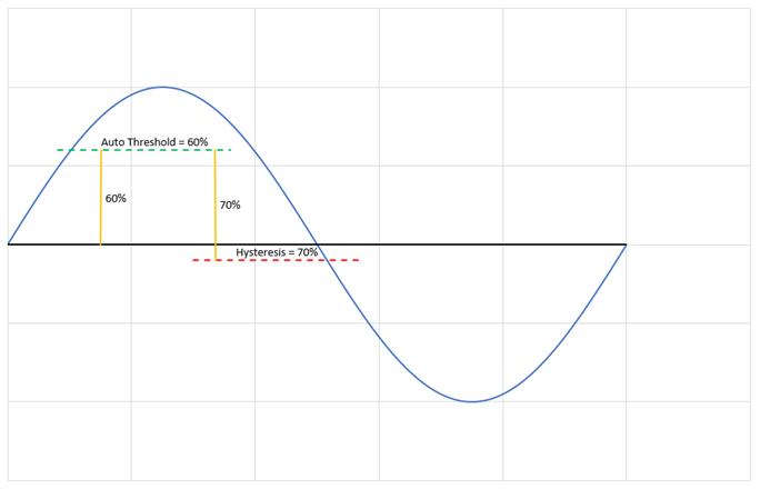
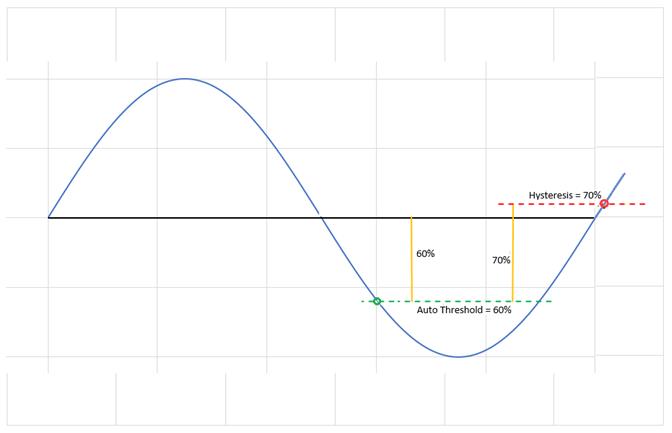
Peak detected value from prior cycle is dynamically used to set the thresholds based on the configuration settings for threshold percent and hysteresis. Peak detection is from either a positive or negative peak.
For channels with Auto Threshold enabled, the upper and lower thresholds will be automatically adjusted based on the channel amplitude measurement, auto threshold percentage setting, and the auto threshold hysteresis setting. Adjustment is done at 1 second intervals.
For rising edge polarity settings:
The upper level will be set to a value of
[ channel amplitude reading X Auto Threshold percentage setting ].
The lower threshold level will be set to a level of
[ upper threshold - ( channel amplitude x Auto Threshold hysteresis % ) ]
For falling edge polarity settings:
The Lower threshold level will be set to a value of
[ -channel amplitude reading X Auto Threshold percentage setting ].
The upper threshold level will be set to a level of
[ lower threshold + ( channel amplitude x Auto Threshold hysteresis % ) ]
Note
channel amplitude measurement is always returned positive, as an absolute number, and represents the peak excursion from 0V, whether negative or positive. Signals are expected to be symmetrical about zero when using this mode. If there is a significant DC offset, then AC coupling or manual threshold settings may be preferable.
Auto Threshold Percent
Sets the percent of peak amplitude to set the active edge threshold in automatic mode. When configured for auto threshold, the trigger threshold is automatically adjusted to the specified percentage of the peak amplitude reading to compensate for varying signal amplitudes, at one second intervals.
Auto Threshold Hysteresis
Sets the percent of hysteresis to set the opposite edge threshold in automatic mode.
Auto Threshold Rising Edge Trigger example
Auto Threshold Falling Edge Trigger example
Termination Enable
Termination is configurable per channel and applies a 50Ω (nominal) termination across the channel input. Termination resistance features a temperature dependent variation (±50%), decreasing with temperature.
A detected signal level measurement greater than 5V will disallow the application of termination resistance and set a Termination Fault status for the channel.
Termination is applicable for damping transients and reflections from high slew rate signals that may alter transition timing.
Channel Enable
Setting a 0 in the corresponding bits for a channel pair (e.g. channels 1 and 2) will reduce the power and suspend operations for those channels.
Reduction in power consumption realized is approximately 120mA or 600mW per channel pair.
Note: There will be no effect if only one of the channels in a pair is disabled, both channels need to be disabled. Channel pairs are 1/2, 3/4, 5/6, 7/8.
Dipole Enable
As initially defined, “Dipole” is defined as the Double Pulse signal type (typically, for discerning phase between the double signal pulses for torque/twist measurement) - this is defined as a reference term within this document. Dipole signal types can be generated and measured as single interleaved double pulse train signals or as paired independent channels with each of the pulse trains on different channels.
When “Dipole Enable” is off (default), the Monopole mode is used for a paired channel phase measurement configuration, with individual synchronous sensor timing references on each channel. Phase measurements will be based on the signal timing from one channel relative to the other. Phase measurement range for monopole measurements is from 0 to 360, with a small uncertainty band about the transition through 360 degrees.
When “Dipole Enable” is enabled (set), Dipole mode is used with a single channel and a signal with two sensor timing references combined and interleaved. The phase measurements are based on the timing of the signals relative to one another.
The designation of primary and secondary timing references is determined based on the minimum time from primary to secondary. Range of phase measurement is from 0 to 180 degrees, with a small uncertainty band about the transition through 180 degrees.
A maximum of eight independent phase measurements is possible with all channels set for dipole. Frequency measurements will be halved compared with monopole mode as there are two timing references on the input.
In monopole mode, the input frequencies on each of the paired channel are expected to be the same, with only a phase difference between the two.
If phase measurements are not required, the channels may operate independently in mixed modes for frequency, counter, and amplitude measurements.
Falling Edge Measurement Enable
This channel configuration selects whether the timing trigger occurs on the rising or falling edge of the input signal. the settings for Voltage Threshold High and Voltage Threshold Low will be used for the trigger thresholds. In rising edge mode, the timing trigger will occur when the signal rises above the High threshold, and resets when the signal subsequently drops below the Low threshold. Any interim transitions of the signal through the High threshold are ignored until the reset occurs. Configuring the levels with greater separation provides hysteresis for better noise immunity.
Conversely, in falling edge mode, the timing trigger occurs when the signal drops below the Low threshold, and resets when the signal rises back above the High threshold.
The threshold settings should be set such that the upper or high threshold is more positive than the lower or low threshold. While the two thresholds can be set to the same value, this may result in erratic measurements in the presence of noise, causing repeated event triggering within the same cycle.
AC-couple Enable
AC Coupling may be used to allow measurement of AC signals with a DC offset, which would require adjustment of the threshold levels.
This mode inserts 10uF capacitors to allow AC signals to propagate through to the measurement circuits while blocking DC components.
Note
Affects the amplitude measurement if the average level is not zero.
Range Select
Configures the internal signal gain for dynamic range vs. resolution.
Using the lowest range that covers the peak signal amplitude provides best measurement stability, while the highest range allows greater tolerance in accommodating high amplitude signals without saturation.
0x0: Auto Range
0x1: ±50mV
0x2: ±100mV
0x3: ±250mV
0x4: ±500mV
0x5: ±1V
0x6: ±2.5V
0x7: ±5V
0x8: ±12.5V
0x9: ±25V
0xA: ±50V
0xB: ±100V
Auto Range setting will continually adjust the gain setting based on the peak amplitude for the channel, updated at 1 second intervals. Note: these updates are independent of the averaging interval selection or the input trigger events.
Auto Down-Range Time
The VR1 has an Auto Gain time configuration feature which will allow the user to delay the down range response of the auto range mode, under conditions where the signal peak amplitude detection remains below a threshold of 80% of the next lower range. Gain range changes will be suppressed for the selected period and limited to one range step per interval, for improved measurement stability.
Upward range changes in response to peaks exceeding 90% of current range will take effect immediately and will not be delayed by this selection. Downward range changes in response to troughs below 40% of the next lower range (delayed by auto downrange time setting).
0x0: 100 ms
0x1: 500 ms
0x2: 1 s
0x3: 2 s
0x4: 5 s
0x5: 10 s
Note
the steps between ranges are not consistently 2x, so the downrange points cannot be defined using only the percentage of current range.
Set Zero Torque Signal Phase
This command strobe will set the phase reference in the Zero Torque Signal Phase register to the last phase measurement reading for the channel and nulls the torque to zero.
e.g. if the last phase measurement was 10 degrees channel 2, strobing this command with a 0x2 will write 10 degrees to the register for the Zero Torque Phase reference.
Torque readings will be based on the difference between the current phase reading and the Zero Torque Phase reference.
Edge or Level Status Trigger
Bit mapped per channel, 0 is Edge triggered, 1 is Level triggered.
Default 0x00 (Edge triggered)
Determines whether the latched status will be triggered only by a transition from a Go status to a No-Go status (Edge triggering), or by the presence of a No-Go condition for the specific status.
In Edge triggered mode, a latched status will not be triggered unless entering the No-Go condition from a Go state. This is primarily to suppress repeated interrupts from being triggered under conditions with a persistent fault. In level triggered mode, the latched status will retrigger as long as the No-Go condition persists.
Test Enable
The test is only run on enabled channels and takes about 1ms to complete.
The signal inputs are disconnected, and a stimulus is applied internally. Then the readings are verified for expected values.
Power Supply Enable
This is a module wide setting.
Writing a value of 1 enables the power supplies (power on default)
Writing a 0 will disable the power supplies for standby power reduction of approx. 500mA. All operations are halted when PS is disabled.
Signal Amplitude Measured
The amplitude is measured by peak sampling the input signal and updated once per second.
The peak reading returned is the magnitude of the greatest excursion from zero, whether positive or negative. The sampling rate is independent of the averaging time configuration.
Cycle Count
Count increments with the rising edge of the input signal as it goes above the upper threshold with rising edge polarity configuration and increments on the falling edge with polarity set for falling edge. Count up mode is presently available, with count down and quadrature counting modes pending implementation.
Signal Phase Measured
Measurement in dipole mode is with two synchronous timing references combined and interleaved on a single channel input in alternating fashion.
Measurement in monopole mode is between a set of paired channels with synchronous phase shifted timing references.
Percent Torque Measured
Percent Torque Measurement is per-channel and based on the following: Max Torque Signal Phase setting, Zero Torque Signal Phase setting, and Phase Measurement value.
The difference between the current phase reading and the Zero Torque Signal Phase setting, divided by the Max Torque Signal Phase, will be the calculated percentage torque.
If the Max Torque signal phase setting is 50 degrees, then a change of +50 degrees from the zero point would be +100% torque. Conversely a change of -50 degrees would be -100% torque.
No limit is placed on the possible torque percentage calculation; values may exceed 100% depending on the scaling.
Examples below:
e.g. if the Zero Torque Signal Phase setting is 14.8 degrees, and the Max Torque Signal Phase is 50 degrees, a Phase Measurement of 47 degrees corresponds to the following percentage torque:
[47 - 14.8] / 50 = 0.644 or 64.4% torque.
e.g. if the Zero Torque Signal Phase setting is 14.8 degrees, and the Max Torque Signal Phase is 20 degrees, a Phase Measurement of 5.2 degrees corresponds to the following percentage torque:
[5.2 - 14.8] / 20 = -0.48 or -48% torque.
Note
when the calculations progress through the 180 degree points (dipole mode) or 360 degree points (in monopole mode), then the measurements are normalized by adding or subtracting 180 or 360 degrees, respectively, to get the smallest torque magnitude.
e.g. For monopole mode, if the Zero Torque Signal Phase setting is 4.8 degrees, and the Max Torque Signal Phase is 20 degrees, a Phase Measurement of 351.2 degrees corresponds to the following percentage torque:
[351.2 - 4.8] = 346.4.
Subtract 360 to get -13.6.
-13.6 / 20 = -0.68 or -68% torque.
e.g. For dipole mode, if the Zero Torque Signal Phase setting is 175 degrees, and the Max Torque Signal Phase is 30 degrees, a phase measurement of 16.8 degrees corresponds to the following percentage torque:
[16.8 - 175] = -158.2.
Add 180 to get 21.8, since the angle crossover for dipole mode is 180 deg.
21.8 / 30 = 0.7267 or 72.67% torque.
Signal Frequency Measured
Frequency measurement in dipole mode will be half of the detected transition frequency as this mode assume two synchronous signals are present and interleaved onto the channel input.
Measurement in monopole mode is individually determined for each channel, based on the frequency of the transition events. Synchronous signals will show the same frequency on each channel of the pair.
Velocity Measured
Displays the revolutions per minute RPM of the shaft, based on frequency scaled by the configuration setting for Number of Teeth.
RPM = Frequency (Hz) * 60 / Number of Teeth. A configuration of Number of Teeth = 60 will result in an RPM reading identical to the frequency.
Amplitude Measurement
The amplitude measurement reading is for the magnitude of the peak excursion from zero (referenced to the Channel (-) input, whether negative or positive.
A DC signal will be read directly.
If a signal ranges from -5 to +2.5V, the amplitude reading will be 5V. A signal range of -3 to 7V will show amplitude reading of 7V.
If AC coupling is enabled for the channel, the zero-level reference will be the average voltage of the signal, with the amplitude reading being the largest excursion from that reference level, rather than the (-) input.
Debounce Time
Filters out noise and unwarranted transition events. Needs to be set to a lower duration than the cycle time of the signal pulses. Note the timing will be affected slightly by the debounce time even in absence of noise, as the transition timing mark will be delayed by the debounce time.
APPENDIX E: PIN-OUT DETAILS
Pin-out details (for reference) are shown below, with respect to DATAIO. Additional information on pin-outs can be found in the Motherboard Operational Manuals.
| Module Signal (Ref Only) | 44-Pin I/O | 50-Pin I/O (Mod Slot 1-J3) | 50-Pin I/O (Mod Slot 2-J4) | 50-Pin I/O (Mod Slot 3-J3) | 50-Pin I/O (Mod Slot 3-J4) | Variable Reluctance/General Purpose Pulse Counter (VR1) |
|---|---|---|---|---|---|---|
| DATIO1 | 2 | 10 | 1 | 2 | CH1 IN+ | |
| DATIO2 | 24 | 35 | 26 | 27 | CH1 IN- | |
| DATIO3 | 3 | 11 | 2 | 3 | CH2 IN+ | |
| DATIO4 | 25 | 36 | 27 | 28 | CH2 IN- | |
| DATIO5 | 5 | 13 | 4 | 5 | ||
| DATIO6 | 27 | 38 | 29 | 30 | ||
| DATIO7 | 7 | 14 | 5 | 6 | CH3 IN+ | |
| DATIO8 | 29 | 39 | 30 | 31 | CH3 IN- | |
| DATIO9 | 8 | 15 | 6 | 7 | CH4 IN+ | |
| DATIO10 | 30 | 40 | 31 | 32 | CH4 IN- | |
| DATIO11 | 10 | 17 | 8 | 9 | ||
| DATIO12 | 32 | 42 | 33 | 34 | ||
| DATIO13 | 12 | 18 | 9 | 17 | CH5 IN+ | |
| DATIO14 | 34 | 43 | 34 | 42 | CH5 IN- | |
| DATIO15 | 13 | 19 | 10 | 18 | CH6 IN+ | |
| DATIO16 | 35 | 44 | 35 | 43 | CH6 IN- | |
| DATIO17 | 15 | 21 | 12 | 20 | ||
| DATIO18 | 37 | 46 | 37 | 45 | ||
| DATIO19 | 17 | 22 | 13 | 21 | CH7 IN+ | |
| DATIO20 | 39 | 47 | 38 | 46 | CH7 IN- | |
| DATIO21 | 18 | 23 | 14 | 22 | CH8 IN+ | |
| DATIO22 | 40 | 48 | 39 | 47 | CH8 IN- | |
| DATIO23 | 20 | 25 | 16 | 24 | ||
| DATIO24 | 42 | 50 | 41 | 49 | ||
| DATIO25 | 4 | 12 | 3 | 4 | ||
| DATIO26 | 26 | 37 | 28 | 29 | ||
| DATIO27 | 9 | 16 | 7 | 8 | ||
| DATIO28 | 31 | 41 | 32 | 33 | ||
| DATIO29 | 14 | 20 | 11 | 19 | ||
| DATIO30 | 36 | 45 | 36 | 44 | ||
| DATIO31 | 19 | 24 | 15 | 23 | ||
| DATIO32 | 41 | 49 | 40 | 48 | ||
| DATIO33 | 6 | |||||
| DATIO34 | 28 | |||||
| DATIO35 | 11 | |||||
| DATIO36 | 33 | |||||
| DATIO37 | 16 | |||||
| DATIO38 | 38 | |||||
| DATIO39 | 21 | |||||
| DATIO40 | 43 | |||||
| N/A |
REVISION HISTORY
| Motherboard Manual - VR1 Revision History | ||
| Revision | Revision Date | Description |
| C | 2022-10-05 | ECO C09440, transition to docbuilder format. Replaced "Specifications" section with "Data Sheet"section. Pg.5-8, removed minimum input voltage range. Pg.5-6, 8 & 10, removed Down Count andQuadrature pulse count modes. Pg.6, updated Input Pulse Resolution & Power specs. Pg.7, addedNote. Pg.8, updated VR Interface resolution bullet. Revised Measurement Register headings (all places). Changed Polarity Select to Falling Edge Measurement Enable (all places). ChangedMinimum Signal Amplitude to Minimum Amplitude (all places). Changed Minimum SignalFrequency to Minimum Frequency (all places). Pg.11, updated Measured Phase integer mode datarange. Pg.12, updated Measured Amplitude function. Pg.13, updated Measured Cycle . Pg.14, added (nominal) to Termination Enable. Pg.16, changed Reluctor Ring to Number of Teeth (Register Descriptions). Pg.16, 28 & 40, added Auto Down-Range Time. Pg.17, updatedSet Zero Torque Signal Phase heading & operational settings. Pg.18, updated Debounce Time integer mode LSB. Pg.18, updated Voltage Threshold High & Low integer mode type/integer mode range/operational settings. Pg.18, updated Minimum Amplitude operational settings. Pg.19,updated Auto Threshold Percent integer mode type/integer mode range/operational settings.Pg.20, updated Auto Threshold Hysteresis integer mode type/integer mode range/operational settings. Pg.28, corrected Auto Threshold Percent Ch 8 offset. Pg.32, added Register NameChanges appendix. Pg.38, added temperature variation text. |
| C1 | 2022-10-11 | ECO C09726, pg.5, changed module designation from Measurement & Simulation Modules to I/OModules. Pg.22, added Signal Loss to Status and Interrupt Registers description. Pg.24, addedSignal Loss to Summary Status register function description. |
| C2 | 2024-02-02 | ECO C11197, pg.9, added product overview. Pg.11/23/29, added Module Common Registers. |
DOCS.NAII REVISIONS
| Revision Date | Description |
|---|---|
| 2025-03-13 | Updated module pinout table to add module I/O pinouts for 44- & 50-pin connectors. |
STATUS AND INTERRUPTS
Status registers indicate the detection of faults or events. The status registers can be channel bit-mapped or event bit-mapped. An example of a channel bit-mapped register is the BIT status register, and an example of an event bit-mapped register is the FIFO status register.
For those status registers that allow interrupts to be generated upon the detection of the fault or the event, there are four registers associated with each status: Dynamic, Latched, Interrupt Enabled, and Set Edge/Level Interrupt.
Dynamic Status: The Dynamic Status register indicates the current condition of the fault or the event. If the fault or the event is momentary, the contents in this register will be clear when the fault or the event goes away. The Dynamic Status register can be polled, however, if the fault or the event is sporadic, it is possible for the indication of the fault or the event to be missed.
Latched Status: The Latched Status register indicates whether the fault or the event has occurred and keeps the state until it is cleared by the user. Reading the Latched Status register is a better alternative to polling the Dynamic Status register because the contents of this register will not clear until the user commands to clear the specific bit(s) associated with the fault or the event in the Latched Status register. Once the status register has been read, the act of writing a 1 back to the applicable status register to any specific bit (channel/event) location will “clear” the bit (set the bit to 0). When clearing the channel/event bits, it is strongly recommended to write back the same bit pattern as read from the Latched Status register. For example, if the channel bit-mapped Latched Status register contains the value 0x0000 0005, which indicates fault/event detection on channel 1 and 3, write the value 0x0000 0005 to the Latched Status register to clear the fault/event status for channel 1 and 3. Writing a “1” to other channels that are not set (example 0x0000 000F) may result in incorrectly “clearing” incoming faults/events for those channels (example, channel 2 and 4).
Interrupt Enable: If interrupts are preferred upon the detection of a fault or an event, enable the specific channel/event interrupt in the Interrupt Enable register. The bits in Interrupt Enable register map to the same bits in the Latched Status register. When a fault or event occurs, an interrupt will be fired. Subsequent interrupts will not trigger until the application acknowledges the fired interrupt by clearing the associated channel/event bit in the Latched Status register. If the interruptible condition is still persistent after clearing the bit, this may retrigger the interrupt depending on the Edge/Level setting.
Set Edge/Level Interrupt: When interrupts are enabled, the condition on retriggering the interrupt after the Latch Register is “cleared” can be specified as “edge” triggered or “level” triggered. Note, the Edge/Level Trigger also affects how the Latched Register value is adjusted after it is “cleared” (see below).
Edge triggered: An interrupt will be retriggered when the Latched Status register change from low (0) to high (1) state. Uses for edge-triggered interrupts would include transition detections (Low-to-High transitions, High-to-Low transitions) or fault detections. After “clearing” an interrupt, another interrupt will not occur until the next transition or the re-occurrence of the fault again.
Level triggered: An interrupt will be generated when the Latched Status register remains at the high (1) state. Level-triggered interrupts are used to indicate that something needs attention.
Interrupt Vector and Steering
When interrupts are enabled, the interrupt vector associated with the specific interrupt can be programmed with a unique number/identifier defined by the user such that it can be utilized in the Interrupt Service Routine (ISR) to identify the type of interrupt. When an interrupt occurs, the contents of the Interrupt Vector registers is reported as part of the interrupt mechanism. In addition to specifying the interrupt vector, the interrupt can be directed (“steered”) to the native bus or to the application running on the onboard ARM processor.
Interrupt Trigger Types
In most applications, limiting the number of interrupts generated is preferred as interrupts are costly, thus choosing the correct Edge/Level interrupt trigger to use is important.
Example 1: Fault detection
This example illustrates interrupt considerations when detecting a fault like an “open” on a line. When an “open” is detected, the system will receive an interrupt. If the “open” on the line is persistent and the trigger is set to “edge”, upon “clearing” the interrupt, the system will not regenerate another interrupt. If, instead, the trigger is set to “level”, upon “clearing” the interrupt, the system will re-generate another interrupt. Thus, in this case, it will be better to set the trigger type to “edge”.
Example 2: Threshold detection
This example illustrates interrupt considerations when detecting an event like reaching or exceeding the “high watermark” threshold value. In a communication device, when the number of elements received in the FIFO reaches the high-watermark threshold, an interrupt will be generated. Normally, the application would read the count of the number of elements in the FIFO and read this number of elements from the FIFO. After reading the FIFO data, the application would “clear” the interrupt. If the trigger type is set to “edge”, another interrupt will be generated only if the number of elements in FIFO goes below the “high watermark” after the “clearing” the interrupt and then fills up to reach the “high watermark” threshold value. Since receiving communication data is inherently asynchronous, it is possible that data can continue to fill the FIFO as the application is pulling data off the FIFO. If, at the time the interrupt is “cleared”, the number of elements in the FIFO is at or above the “high watermark”, no interrupts will be generated. In this case, it will be better to set the trigger type to “level”, as the purpose here is to make sure that the FIFO is serviced when the number of elements exceeds the high watermark threshold value. Thus, upon “clearing” the interrupt, if the number of elements in the FIFO is at or above the “high watermark” threshold value, another interrupt will be generated indicating that the FIFO needs to be serviced.
Dynamic and Latched Status Registers Examples
The examples in this section illustrate the differences in behavior of the Dynamic Status and Latched Status registers as well as the differences in behavior of Edge/Level Trigger when the Latched Status register is cleared.
Figure 1. Example of Module's Channel-Mapped Dynamic and Latched Status States
No Clearing of
Latched StatusClearing of Latched Status
(Edge-Triggered)Clearing of Latched Status
(Level-Triggered)Time Dynamic Status Latched Status Action Latched Status Action Latched T0 0x0 0x0 Read Latched Register 0x0 Read Latched Register 0x0 T1 0x1 0x1 Read Latched Register 0x1 0x1 T1 0x1 0x1 Write 0x1 to Latched Register Write 0x1 to Latched Register T1 0x1 0x1 0x0 0x1 T2 0x0 0x1 Read Latched Register 0x0 Read Latched Register 0x1 T2 0x0 0x1 Read Latched Register 0x0 Write 0x1 to Latched Register T2 0x0 0x1 Read Latched Register 0x0 0x0 T3 0x2 0x3 Read Latched Register 0x2 Read Latched Register 0x2 T3 0x2 0x3 Write 0x2 to Latched Register Write 0x2 to Latched Register T3 0x2 0x3 0x0 0x2 T4 0x2 0x3 Read Latched Register 0x1 Read Latched Register 0x3 T4 0x2 0x3 Write 0x1 to Latched Register Write 0x3 to Latched Register T4 0x2 0x3 0x0 0x2 T5 0xC 0xF Read Latched Register 0xC Read Latched Register 0xE T5 0xC 0xF Write 0xC to Latched Register Write 0xE to Latched Register T5 0xC 0xF 0x0 0xC T6 0xC 0xF Read Latched Register 0x0 Read Latched 0xC T6 0xC 0xF Read Latched Register 0x0 Write 0xC to Latched Register T6 0xC 0xF Read Latched Register 0x0 0xC T7 0x4 0xF Read Latched Register 0x0 Read Latched Register 0xC T7 0x4 0xF Read Latched Register 0x0 Write 0xC to Latched Register T7 0x4 0xF Read Latched Register 0x0 0x4 T8 0x4 0xF Read Latched Register 0x0 Read Latched Register 0x4 Interrupt Examples
The examples in this section illustrate the interrupt behavior with Edge/Level Trigger.
Figure 2. Illustration of Latched Status State for Module with 4-Channels with Interrupt Enabled
Time Latched Status
(Edge-Triggered -
Clear Multi-Channel)Latched Status
(Edge-Triggered -
Clear Single Channel)Latched Status
(Level-Triggered -
Clear Multi-Channel)Action Latched Action Latched Action Latched T1
(Int 1)Interrupt Generated
Read Latched Registers0x1 Interrupt Generated
Read Latched Registers0x1 Interrupt Generated
Read Latched Registers0x1 T1
(Int 1)Write 0x1 to Latched Register Write 0x1 to Latched Register Write 0x1 to Latched Register T1
(Int 1)0x0 0x0 Interrupt re-triggers
Note, interrupt re-triggers after
each clear until T2.0x1 T3
(Int 2)Interrupt Generated
Read Latched Registers0x2 Interrupt Generated
Read Latched Registers0x2 Interrupt Generated
Read Latched Registers0x2 T3
(Int 2)Write 0x2 to Latched Register Write 0x2 to Latched Register Write 0x2 to Latched Register T3
(Int 2)0x0 0x0 Interrupt re-triggers
Note, interrupt re-triggers after
each clear until T7.0x2 T4
(Int 3)Interrupt Generated
Read Latched Registers0x1 Interrupt Generated
Read Latched Registers0x1 Interrupt Generated
Read Latched Registers0x3 T4
(Int 3)Write 0x1 to Latched Register Write 0x1 to Latched Register Write 0x3 to Latched Register T4
(Int 3)0x0 0x0 Interrupt re-triggers
Note, interrupt re-triggers after
each clear and 0x3 is reported
in Latched Register until T5.0x3 T4
(Int 3)0x0 0x0 Interrupt re-triggers
Note, interrupt re-triggers after
each clear until T7.0x2 T6
(Int 4)Interrupt Generated
Read Latched Registers0xC Interrupt Generated
Read Latched Registers0xC Interrupt Generated
Read Latched Registers0xE T6
(Int 4)Write 0xC to Latched Register Write 0x4 to Latched Register Write 0xE to Latched Register T6
(Int 4)0x0 Interrupt re-triggers
Write 0x8 to Latched Register0x8 Interrupt re-triggers
Note, interrupt re-triggers after
each clear and 0xE is
reported in Latched Register until T7.0xE T6
(Int 4)0x0 0x0 Interrupt re-triggers
Note, interrupt re-triggers after
each clear and 0xC is
reported in Latched Register until T8.0xC T6
(Int 4)0x0 0x0 Interrupt re-triggers
Note, interrupt re-triggers after
each clear and 0x4 is
reported in Latched Register always.0x4 REVISION HISTORY
Motherboard Manual - Status and Interrupts Revision History Revision Revision Date Description C 2021-11-30 C08896; Transition manual to docbuilder format - no technical info change. Link to original
DOCS.NAII REVISIONS Revision Date Description 2026-03-02 Formatting updates to document; no technical changes. 2026-05-18 Fixed formatting issues from conversion to new doc site format. 2026-05-19 Fixed minor formatting issue with Interrupt Examples table structure (removed extraneous cell). 2026-07-15 Revised image files for image quality.
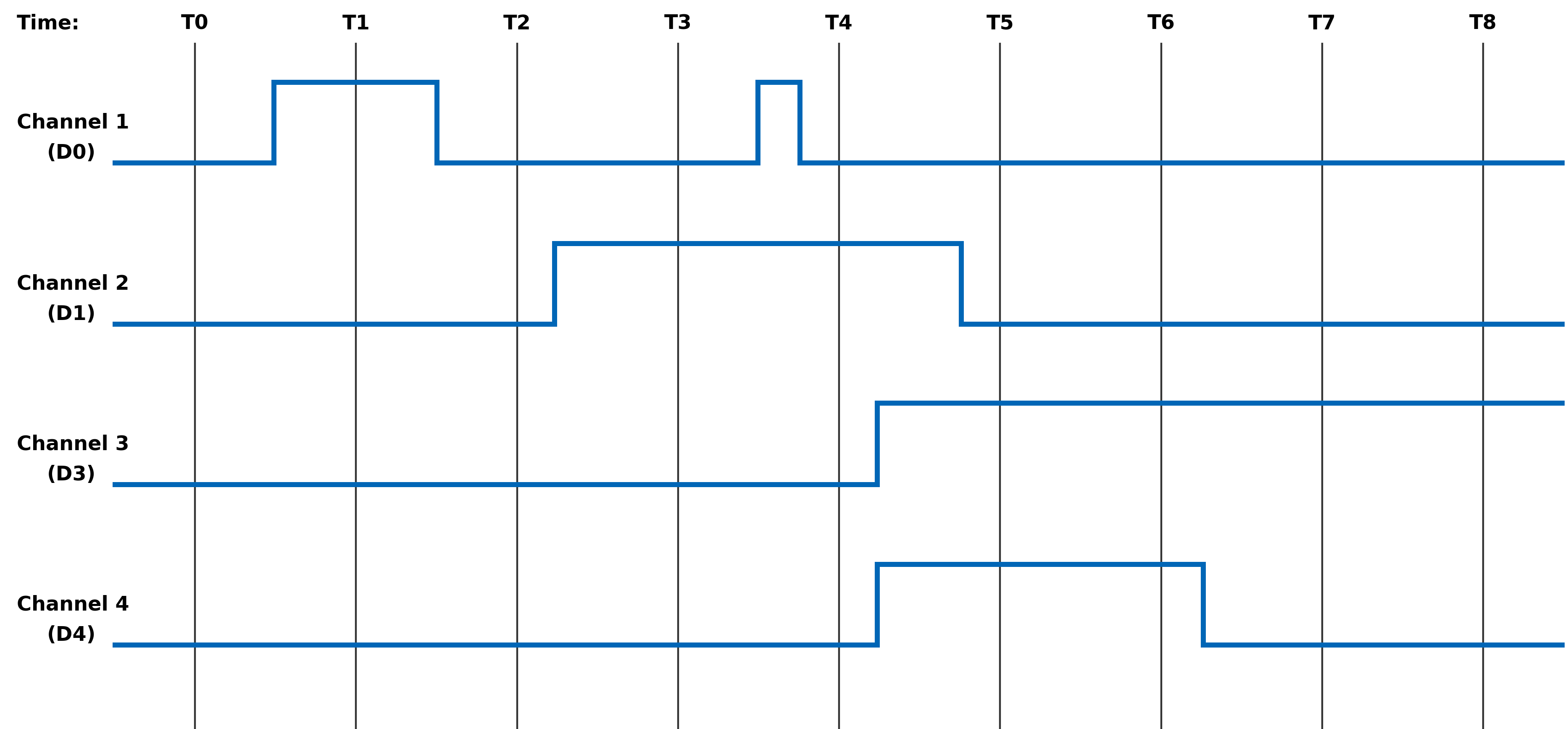
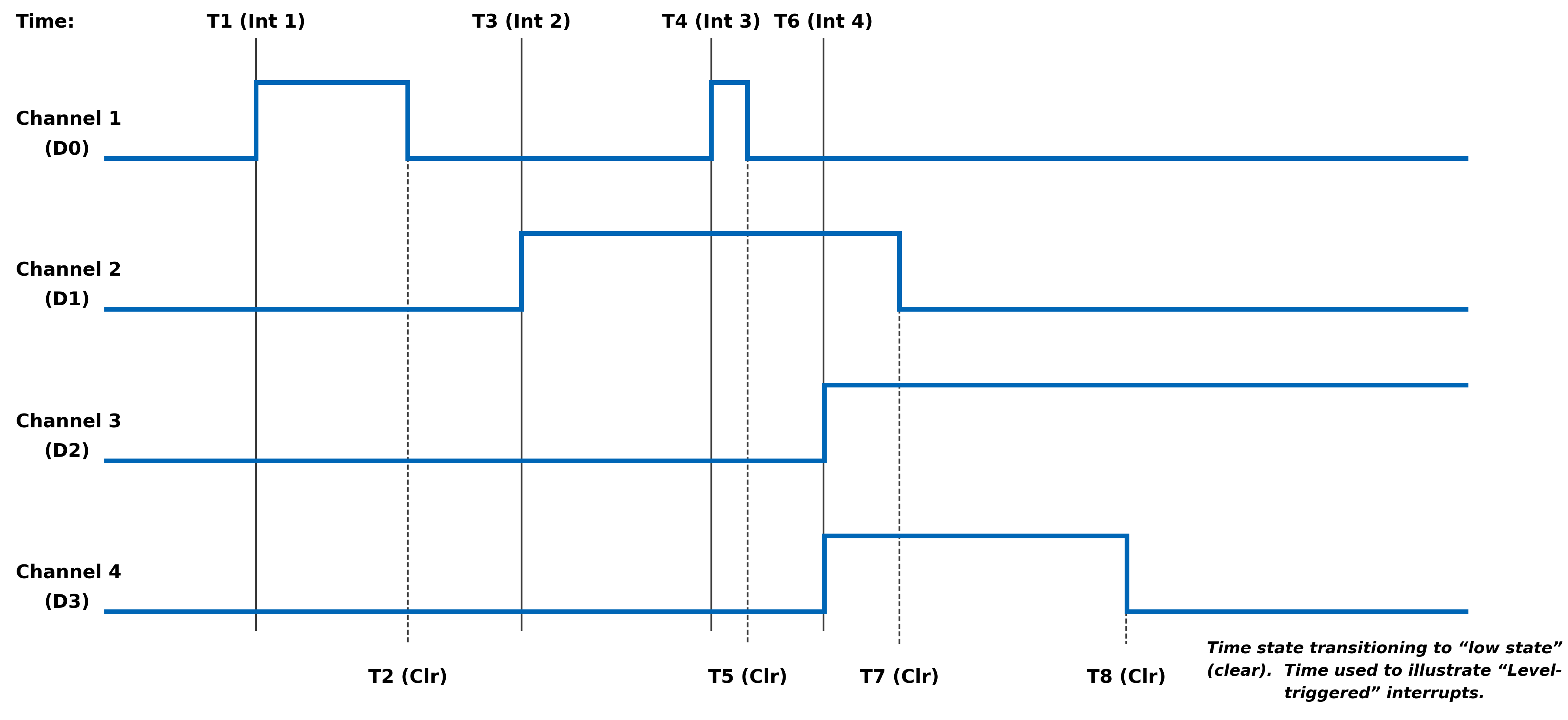
MODULE COMMON REGISTERS
The registers described in this document are common to all NAI Generation 5 modules.
Module Information Registers
The registers in this section provide module information such as firmware revisions, capabilities and unique serial number information.
FPGA Version Registers
The FPGA firmware version registers include registers that contain the Revision, Compile Timestamp, SerDes Revision, Template Revision and Zynq Block Revision information.
FPGA Revision Function: FPGA firmware revision Type: unsigned binary word (32-bit) Data Range: 0x0000 0000 to 0xFFFF FFFF Read/Write: R Initialized Value: Value corresponding to the revision of the board's FPGA Operational Settings: The upper 16-bits are the major revision and the lower 16-bits are the minor revision.
D31 D30 D29 D28 D27 D26 D25 D24 D23 D22 D21 D20 D19 D18 D17 D16 Major Revision Number D15 D14 D13 D12 D11 D10 D9 D8 D7 D6 D5 D4 D3 D2 D1 D0 Minor Revision Number
FPGA Compile Timestamp Function: Compile Timestamp for the FPGA firmware. Type: unsigned binary word (32-bit) Data Range: N/A Read/Write: R Initialized Value: Value corresponding to the compile timestamp of the board's FPGA Operational Settings: The 32-bit value represents the Day, Month, Year, Hour, Minutes and Seconds as formatted in the table:
D31 D30 D29 D28 D27 D26 D25 D24 D23 D22 D21 D20 D19 D18 D17 D16 day (5-bits) month (4-bits) year (6-bits) hr D15 D14 D13 D12 D11 D10 D9 D8 D7 D6 D5 D4 D3 D2 D1 D0 hour (5-bits) minutes (6-bits) seconds (6-bits)
FPGA SerDes Revision Function: FPGA SerDes revision Type: unsigned binary word (32-bit) Data Range: 0x0000 0000 to 0xFFFF FFFF Read/Write: R Initialized Value: Value corresponding to the SerDes revision of the board's FPGA Operational Settings: The upper 16-bits are the major revision, and the lower 16-bits are the minor revision.
D31 D30 D29 D28 D27 D26 D25 D24 D23 D22 D21 D20 D19 D18 D17 D16 Major Revision Number D15 D14 D13 D12 D11 D10 D9 D8 D7 D6 D5 D4 D3 D2 D1 D0 Minor Revision Number
FPGA Template Revision Function: FPGA Template revision Type: unsigned binary word (32-bit) Data Range: 0x0000 0000 to 0xFFFF FFFF Read/Write: R Initialized Value: Value corresponding to the template revision of the board's FPGA Operational Settings: The upper 16-bits are the major revision, and the lower 16-bits are the minor revision.
D31 D30 D29 D28 D27 D26 D25 D24 D23 D22 D21 D20 D19 D18 D17 D16 Major Revision Number D15 D14 D13 D12 D11 D10 D9 D8 D7 D6 D5 D4 D3 D2 D1 D0 Minor Revision Number
FPGA Zynq Block Revision Function: FPGA Zynq Block revision Type: unsigned binary word (32-bit) Data Range: 0x0000 0000 to 0xFFFF FFFF Read/Write: R Initialized Value: Value corresponding to the Zynq block revision of the board's FPGA Operational Settings: The upper 16-bits are the major revision, and the lower 16-bits are the minor revision.
D31 D30 D29 D28 D27 D26 D25 D24 D23 D22 D21 D20 D19 D18 D17 D16 Major Revision Number D15 D14 D13 D12 D11 D10 D9 D8 D7 D6 D5 D4 D3 D2 D1 D0 Minor Revision Number Bare Metal Version Registers
The Bare Metal firmware version registers include registers that contain the Revision and Compile Time information.
Bare Metal Revision Function: Bare Metal firmware revision Type: unsigned binary word (32-bit) Data Range: 0x0000 0000 to 0xFFFF FFFF Read/Write: R Initialized Value: Value corresponding to the revision of the board's Bare Metal Operational Settings: The upper 16-bits are the major revision and the lower 16-bits are the minor revision.
D31 D30 D29 D28 D27 D26 D25 D24 D23 D22 D21 D20 D19 D18 D17 D16 Major Revision Number D15 D14 D13 D12 D11 D10 D9 D8 D7 D6 D5 D4 D3 D2 D1 D0 Minor Revision Number
Bare Metal Compile Time Function: Provides an ASCII representation of the Date/Time for the Bare Metal compile time. Type: 24-character ASCII string - Six (6) unsigned binary word (32-bit) Data Range: N/A Read/Write: R Initialized Value: Value corresponding to the ASCII representation of the compile time of the board's Bare Metal Operational Settings: The six 32-bit words provide an ASCII representation of the Date/Time. The hexadecimal values in the field below represent: May 17 2019 at 15:38:32 Note
little-endian order of ASCII values
Word 1 (Ex. 0x2079614D) D31 D30 D29 D28 D27 D26 D25 D24 D23 D22 D21 D20 D19 D18 D17 D16 Space (0x20) Month ('y' - 0x79) D15 D14 D13 D12 D11 D10 D9 D8 D7 D6 D5 D4 D3 D2 D1 D0 Month ('a' - 0x61) Month ('M' - 0x4D) Word 2 (Ex. 0x32203731) D31 D30 D29 D28 D27 D26 D25 D24 D23 D22 D21 D20 D19 D18 D17 D16 Year ('2' - 0x32) Space (0x20) D15 D14 D13 D12 D11 D10 D9 D8 D7 D6 D5 D4 D3 D2 D1 D0 Day ('7' - 0x37) Day ('1' - 0x31) Word 3 (Ex. 0x20393130) D31 D30 D29 D28 D27 D26 D25 D24 D23 D22 D21 D20 D19 D18 D17 D16 Space (0x20) Year ('9' - 0x39) D15 D14 D13 D12 D11 D10 D9 D8 D7 D6 D5 D4 D3 D2 D1 D0 Year ('1' - 0x31) Year ('0' - 0x30) Word 4 (Ex. 0x31207461) D31 D30 D29 D28 D27 D26 D25 D24 D23 D22 D21 D20 D19 D18 D17 D16 Hour ('1' - 0x31) Space (0x20) D15 D14 D13 D12 D11 D10 D9 D8 D7 D6 D5 D4 D3 D2 D1 D0 'a' (0x74) 't' (0x61) Word 5 (Ex. 0x38333A35) D31 D30 D29 D28 D27 D26 D25 D24 D23 D22 D21 D20 D19 D18 D17 D16 Minute ('8' - 0x38) Minute ('3' - 0x33) D15 D14 D13 D12 D11 D10 D9 D8 D7 D6 D5 D4 D3 D2 D1 D0 ':' (0x3A) Hour ('5' - 0x35) Word 6 (Ex. 0x0032333A) D31 D30 D29 D28 D27 D26 D25 D24 D23 D22 D21 D20 D19 D18 D17 D16 NULL (0x00) Seconds ('2' - 0x32) D15 D14 D13 D12 D11 D10 D9 D8 D7 D6 D5 D4 D3 D2 D1 D0 Seconds ('3' - 0x33) ':' (0x3A) FSBL Version Registers
The FSBL version registers include registers that contain the Revision and Compile Time information for the First Stage Boot Loader (FSBL).
FSBL Revision Function: FSBL firmware revision Type: unsigned binary word (32-bit) Data Range: 0x0000 0000 to 0xFFFF FFFF Read/Write: R Initialized Value: Value corresponding to the revision of the board's FSBL Operational Settings: The upper 16-bits are the major revision, and the lower 16-bits are the minor revision.
D31 D30 D29 D28 D27 D26 D25 D24 D23 D22 D21 D20 D19 D18 D17 D16 Major Revision Number D15 D14 D13 D12 D11 D10 D9 D8 D7 D6 D5 D4 D3 D2 D1 D0 Minor Revision Number
FSBL Compile Time Function: Provides an ASCII representation of the Date/Time for the FSBL compile time. Type: 24-character ASCII string - Six (6) unsigned binary word (32-bit) Data Range: N/A Read/Write: R Initialized Value: Value corresponding to the ASCII representation of the Compile Time of the board's FSBL Operational Settings: The six 32-bit words provide an ASCII representation of the Date/Time. The hexadecimal values in the field below represent: May 17 2019 at 15:38:32
Note
little-endian order of ASCII values
Word 1 (Ex. 0x2079614D) D31 D30 D29 D28 D27 D26 D25 D24 D23 D22 D21 D20 D19 D18 D17 D16 Space (0x20) Month ('y' - 0x79) D15 D14 D13 D12 D11 D10 D9 D8 D7 D6 D5 D4 D3 D2 D1 D0 Month ('a' - 0x61) Month ('M' - 0x4D) Word 2 (Ex. 0x32203731) D31 D30 D29 D28 D27 D26 D25 D24 D23 D22 D21 D20 D19 D18 D17 D16 Year ('2' - 0x32) Space (0x20) D15 D14 D13 D12 D11 D10 D9 D8 D7 D6 D5 D4 D3 D2 D1 D0 Day ('7' - 0x37) Day ('1' - 0x31) Word 3 (Ex. 0x20393130) D31 D30 D29 D28 D27 D26 D25 D24 D23 D22 D21 D20 D19 D18 D17 D16 Space (0x20) Year ('9' - 0x39) D15 D14 D13 D12 D11 D10 D9 D8 D7 D6 D5 D4 D3 D2 D1 D0 Year ('1' - 0x31) Year ('0' - 0x30) Word 4 (Ex. 0x31207461) D31 D30 D29 D28 D27 D26 D25 D24 D23 D22 D21 D20 D19 D18 D17 D16 Hour ('1' - 0x31) Space (0x20) D15 D14 D13 D12 D11 D10 D9 D8 D7 D6 D5 D4 D3 D2 D1 D0 'a' (0x74) 't' (0x61) Word 5 (Ex. 0x38333A35) D31 D30 D29 D28 D27 D26 D25 D24 D23 D22 D21 D20 D19 D18 D17 D16 Minute ('8' - 0x38) Minute ('3' - 0x33) D15 D14 D13 D12 D11 D10 D9 D8 D7 D6 D5 D4 D3 D2 D1 D0 ':' (0x3A) Hour ('5' - 0x35) Word 6 (Ex. 0x0032333A) D31 D30 D29 D28 D27 D26 D25 D24 D23 D22 D21 D20 D19 D18 D17 D16 NULL (0x00) Seconds ('2' - 0x32) D15 D14 D13 D12 D11 D10 D9 D8 D7 D6 D5 D4 D3 D2 D1 D0 Seconds ('3' - 0x33) ':' (0x3A) Module Serial Number Registers
The Module Serial Number registers include registers that contain the Serial Numbers for the Interface Board and the Functional Board of the module.
Interface Board Serial Number Function: Unique 128-bit identifier used to identify the interface board. Type: 16-character ASCII string - Four (4) unsigned binary words (32-bit) Data Range: N/A Read/Write: R Initialized Value: Serial number of the interface board Operational Settings: This register is for information purposes only.
Functional Board Serial Number Function: Unique 128-bit identifier used to identify the functional board. Type: 16-character ASCII string - Four (4) unsigned binary words (32-bit) Data Range: N/A Read/Write: R Initialized Value: Serial number of the functional board Operational Settings: This register is for information purposes only.
Module Capability Function: Provides indication for whether or not the module can support the following: SerDes block reads, SerDes FIFO block reads, SerDes packing (combining two 16-bit values into one 32-bit value) and floating point representation. The purpose for block access and packing is to improve the performance of accessing larger amounts of data over the SerDes interface. Type: unsigned binary word (32-bit) Data Range: 0x0000 0000 to 0x0000 0107 Read/Write: R Initialized Value: 0x0000 0107 Operational Settings: A “1” in the bit associated with the capability indicates that it is supported.
D31 D30 D29 D28 D27 D26 D25 D24 D23 D22 D21 D20 D19 D18 D17 D16 0 0 0 0 0 0 0 0 0 0 0 0 0 0 0 0 D15 D14 D13 D12 D11 D10 D9 D8 D7 D6 D5 D4 D3 D2 D1 D0 0 0 0 0 0 0 0 Flt-Pt 0 0 0 0 0 Pack FIFO Blk Blk
Module Memory Map Revision Function: Module Memory Map revision Type: unsigned binary word (32-bit) Data Range: 0x0000 0000 to 0xFFFF FFFF Read/Write: R Initialized Value: Value corresponding to the Module Memory Map Revision Operational Settings: The upper 16-bits are the major revision and the lower 16-bits are the minor revision.
D31 D30 D29 D28 D27 D26 D25 D24 D23 D22 D21 D20 D19 D18 D17 D16 Major Revision Number D15 D14 D13 D12 D11 D10 D9 D8 D7 D6 D5 D4 D3 D2 D1 D0 Minor Revision Number Module Measurement Registers
The registers in this section provide module temperature measurement information.
Temperature Readings Registers
The temperature registers provide the current, maximum (from power-up) and minimum (from power-up) Zynq and PCB temperatures.
Interface Board Current Temperature Function: Measured PCB and Zynq Core temperatures on Interface Board. Type: signed byte (8-bits) for PCB and signed byte (8-bits) for Zynq core temperatures Data Range: 0x0000 0000 to 0x0000 FFFF Read/Write: R Initialized Value: Value corresponding to the measured PCB and Zynq core temperatures based on the table below Operational Settings: The upper 16-bits are not used, and the lower 16-bits are the PCB and Zynq Core Temperatures. For example, if the register contains the value 0x0000 202C, this represents PCB Temperature = 32° Celsius and Zynq Temperature = 44° Celsius.
D31 D30 D29 D28 D27 D26 D25 D24 D23 D22 D21 D20 D19 D18 D17 D16 0 0 0 0 0 0 0 0 0 0 0 0 0 0 0 0 D15 D14 D13 D12 D11 D10 D9 D8 D7 D6 D5 D4 D3 D2 D1 D0 PCB Temperature Zynq Core Temperature
Functional Board Current Temperature Function: Measured PCB temperature on Functional Board. Type: signed byte (8-bits) for PCB Data Range: 0x0000 0000 to 0x0000 00FF Read/Write: R Initialized Value: Value corresponding to the measured PCB on the table below Operational Settings: The upper 24-bits are not used, and the lower 8-bits are the PCB Temperature. For example, if the register contains the value 0x0000 0019, this represents PCB Temperature = 25° Celsius.
D31 D30 D29 D28 D27 D26 D25 D24 D23 D22 D21 D20 D19 D18 D17 D16 0 0 0 0 0 0 0 0 0 0 0 0 0 0 0 0 D15 D14 D13 D12 D11 D10 D9 D8 D7 D6 D5 D4 D3 D2 D1 D0 0 0 0 0 0 0 0 0 PCB Temperature
Interface Board Maximum Temperature Function: Maximum PCB and Zynq Core temperatures on Interface Board since power-on. Type: signed byte (8-bits) for PCB and signed byte (8-bits) for Zynq core temperatures Data Range: 0x0000 0000 to 0x0000 FFFF Read/Write: R Initialized Value: Value corresponding to the maximum measured PCB and Zynq core temperatures since power-on based on the table below Operational Settings: The upper 16-bits are not used, and the lower 16-bits are the maximum PCB and Zynq Core Temperatures. For example, if the register contains the value 0x0000 5569, this represents maximum PCB Temperature = 85° Celsius and maximum Zynq Temperature = 105° Celsius.
D31 D30 D29 D28 D27 D26 D25 D24 D23 D22 D21 D20 D19 D18 D17 D16 0 0 0 0 0 0 0 0 0 0 0 0 0 0 0 0 D15 D14 D13 D12 D11 D10 D9 D8 D7 D6 D5 D4 D3 D2 D1 D0 PCB Temperature Zynq Core Temperature
Interface Board Minimum Temperature Function: Minimum PCB and Zynq Core temperatures on Interface Board since power-on. Type: signed byte (8-bits) for PCB and signed byte (8-bits) for Zynq core temperatures Data Range: 0x0000 0000 to 0x0000 FFFF Read/Write: R Initialized Value: Value corresponding to the minimum measured PCB and Zynq core temperatures since power-on based on the table below Operational Settings: The upper 16-bits are not used, and the lower 16-bits are the minimum PCB and Zynq Core Temperatures. For example, if the register contains the value 0x0000 D8E7, this represents minimum PCB Temperature = -40° Celsius and minimum Zynq Temperature = -25° Celsius.
D31 D30 D29 D28 D27 D26 D25 D24 D23 D22 D21 D20 D19 D18 D17 D16 0 0 0 0 0 0 0 0 0 0 0 0 0 0 0 0 D15 D14 D13 D12 D11 D10 D9 D8 D7 D6 D5 D4 D3 D2 D1 D0 PCB Temperature Zynq Core Temperature
Functional Board Maximum Temperature Function: Maximum PCB temperature on Functional Board since power-on. Type: signed byte (8-bits) for PCB Data Range: 0x0000 0000 to 0x0000 00FF Read/Write: R Initialized Value: Value corresponding to the measured PCB on the table below Operational Settings: The upper 24-bits are not used, and the lower 8-bits are the PCB Temperature. For example, if the register contains the value 0x0000 0055, this represents PCB Temperature = 85° Celsius.
D31 D30 D29 D28 D27 D26 D25 D24 D23 D22 D21 D20 D19 D18 D17 D16 0 0 0 0 0 0 0 0 0 0 0 0 0 0 0 0 D15 D14 D13 D12 D11 D10 D9 D8 D7 D6 D5 D4 D3 D2 D1 D0 0 0 0 0 0 0 0 0 PCB Temperature
Functional Board Minimum Temperature Function: Minimum PCB temperature on Functional Board since power-on. Type: signed byte (8-bits) for PCB Data Range: 0x0000 0000 to 0x0000 00FF Read/Write: R Initialized Value: Value corresponding to the measured PCB on the table below Operational Settings: The upper 24-bits are not used, and the lower 8-bits are the PCB Temperature. For example, if the register contains the value 0x0000 00D8, this represents PCB Temperature = -40° Celsius.
D31 D30 D29 D28 D27 D26 D25 D24 D23 D22 D21 D20 D19 D18 D17 D16 0 0 0 0 0 0 0 0 0 0 0 0 0 0 0 0 D15 D14 D13 D12 D11 D10 D9 D8 D7 D6 D5 D4 D3 D2 D1 D0 0 0 0 0 0 0 0 0 PCB Temperature Higher Precision Temperature Readings Registers
These registers provide higher precision readings of the current Zynq and PCB temperatures.
Higher Precision Zynq Core Temperature Function: Higher precision measured Zynq Core temperature on Interface Board. Type: signed word (16-bits) for integer part and unsigned word (16-bits) for fractional part Data Range: 0x0000 0000 to 0xFFFF FFFF Read/Write: R Initialized Value: Measured Zynq Core temperature on Interface Board Operational Settings: The upper 16-bits represent the signed integer part of the temperature and the lower 16-bits represent the fractional part of the temperature with the resolution of 1/1000 of degree Celsius. For example, if the register contains the value 0x002B 0271, this represents Zynq Core Temperature = 43.625° Celsius, and value 0xFFF6 0177 represents -10.375° Celsius.
D31 D30 D29 D28 D27 D26 D25 D24 D23 D22 D21 D20 D19 D18 D17 D16 Signed Integer Part of Temperature D15 D14 D13 D12 D11 D10 D9 D8 D7 D6 D5 D4 D3 D2 D1 D0 Fractional Part of Temperature
Higher Precision Interface PCB Temperature Function: Higher precision measured Interface PCB temperature. Type: signed word (16-bits) for integer part and unsigned word (16-bits) for fractional part Data Range: 0x0000 0000 to 0xFFFF FFFF Read/Write: R Initialized Value: Measured Interface PCB temperature Operational Settings: The upper 16-bits represent the signed integer part of the temperature and the lower 16-bits represent the fractional part of the temperature with the resolution of 1/1000 of degree Celsius. For example, if the register contains the value 0x0020 007D, this represents Interface PCB Temperature = 32.125° Celsius, and value 0xFFE8 036B represents -24.875° Celsius.
D31 D30 D29 D28 D27 D26 D25 D24 D23 D22 D21 D20 D19 D18 D17 D16 Signed Integer Part of Temperature D15 D14 D13 D12 D11 D10 D9 D8 D7 D6 D5 D4 D3 D2 D1 D0 Fractional Part of Temperature
Higher Precision Functional PCB Temperature Function: Higher precision measured Functional PCB temperature. Type: signed word (16-bits) for integer part and unsigned word (16-bits) for fractional part Data Range: 0x0000 0000 to 0xFFFF FFFF Read/Write: R Initialized Value: Measured Functional PCB temperature Operational Settings: The upper 16-bits represent the signed integer part of the temperature and the lower 16-bits represent the fractional part of the temperature with the resolution of 1/100 of degree Celsius. For example, if the register contains the value 0x0018 004B, this represents Functional PCB Temperature = 24.75° Celsius, and value 0xFFD9 0019 represents -39.25° Celsius.
D31 D30 D29 D28 D27 D26 D25 D24 D23 D22 D21 D20 D19 D18 D17 D16 Signed Integer Part of Temperature D15 D14 D13 D12 D11 D10 D9 D8 D7 D6 D5 D4 D3 D2 D1 D0 Fractional Part of Temperature Module Health Monitoring Registers
The registers in this section provide module temperature measurement information. If the temperature measurements reaches the Lower Critical or Upper Critical conditions, the module will automatically reset itself to prevent damage to the hardware.
Module Sensor Summary Status Function: The corresponding sensor bit is set if the sensor has crossed any of its thresholds. Type: unsigned binary word (32-bits) Data Range: See table below Read/Write: R Initialized Value: 0 Operational Settings: This register provides a summary for module sensors. When the corresponding sensor bit is set, the Sensor Threshold Status register for that sensor will indicate the threshold condition that triggered the event.
Bit(s) Sensor D31:D6 Reserved D5 Functional Board PCB Temperature D4 Interface Board PCB Temperature D3:D0 Reserved Module Sensor Registers
The registers listed in this section apply to each module sensor listed for the Module Sensor Summary Status register. Each individual sensor register provides a group of registers for monitoring module temperatures readings. From these registers, a user can read the current temperature of the sensor in addition to the minimum and maximum temperature readings since power-up. Upper and lower critical/warning temperature thresholds can be set and monitored from these registers. When a programmed temperature threshold is crossed, the Sensor Threshold Status register will set the corresponding bit for that threshold. The figure below shows the functionality of this group of registers when accessing the Interface Board PCB Temperature sensor as an example.
Sensor Threshold Status Function: Reflects which threshold has been crossed Type: unsigned binary word (32-bits) Data Range: See table below Read/Write: R Initialized Value: 0 Operational Settings: The associated bit is set when the sensor reading exceed the corresponding threshold settings.
Bit(s) Description D31:D4 Reserved D3 Exceeded Upper Critical Threshold D2 Exceeded Upper Warning Threshold D1 Exceeded Lower Critical Threshold D0 Exceeded Lower Warning Threshold
Sensor Current Reading Function: Reflects current reading of temperature sensor Type: Single Precision Floating Point Value (IEEE-754) Data Range: Single Precision Floating Point Value (IEEE-754) Read/Write: R Initialized Value: N/A Operational Settings: The register represents current sensor reading as a single precision floating point value. For example, for a temperature sensor, register value 0x41C6 0000 represents temperature = 24.75° Celsius.
Sensor Minimum Reading Function: Reflects minimum value of temperature sensor since power up Type: Single Precision Floating Point Value (IEEE-754) Data Range: Single Precision Floating Point Value (IEEE-754) Read/Write: R Initialized Value: N/A Operational Settings: The register represents minimum sensor value as a single precision floating point value. For example, for a temperature sensor, register value 0x41C6 0000 represents temperature = 24.75° Celsius.
Sensor Maximum Reading Function: Reflects maximum value of temperature sensor since power up Type: Single Precision Floating Point Value (IEEE-754) Data Range: Single Precision Floating Point Value (IEEE-754) Read/Write: R Initialized Value: N/A Operational Settings: The register represents maximum sensor value as a single precision floating point value. For example, for a temperature sensor, register value 0x41C6 0000 represents temperature = 24.75° Celsius.
Sensor Lower Warning Threshold Function: Reflects lower warning threshold of temperature sensor Type: Single Precision Floating Point Value (IEEE-754) Data Range: Single Precision Floating Point Value (IEEE-754) Read/Write: R/W Initialized Value: Default lower warning threshold (value dependent on specific sensor) Operational Settings: The register represents sensor lower warning threshold as a single precision floating point value. For example, for a temperature sensor, register value 0xC220 0000 represents temperature = -40.0° Celsius.
Sensor Lower Critical Threshold Function: Reflects lower critical threshold of temperature sensor Type: Single Precision Floating Point Value (IEEE-754) Data Range: Single Precision Floating Point Value (IEEE-754) Read/Write: R/W Initialized Value: Default lower critical threshold (value dependent on specific sensor) Operational Settings: The register represents sensor lower critical threshold as a single precision floating point value. For example, for a temperature sensor, register value 0xC25C 0000 represents temperature = -55.0° Celsius.
Sensor Upper Warning Threshold Function: Reflects upper warning threshold of temperature sensor Type: Single Precision Floating Point Value (IEEE-754) Data Range: Single Precision Floating Point Value (IEEE-754) Read/Write: R/W Initialized Value: Default upper warning threshold (value dependent on specific sensor) Operational Settings: The register represents sensor upper warning threshold as a single precision floating point value. For example, for a temperature sensor, register value 0x42AA 0000 represents temperature = 85.0° Celsius.
Sensor Upper Critical Threshold Function: Reflects upper critical threshold of temperature sensor Type: Single Precision Floating Point Value (IEEE-754) Data Range: Single Precision Floating Point Value (IEEE-754) Read/Write: R/W Initialized Value: Default upper critical threshold (value dependent on specific sensor) Operational Settings: The register represents sensor upper critical threshold as a single precision floating point value. For example, for a temperature sensor, register value 0x42FA 0000 represents temperature = 125.0° Celsius. FUNCTION REGISTER MAP
KEY
Configuration/Control Measurement/Status/Board Information
MODULE INFORMATION REGISTERS OFFSET REGISTER NAME ACCESS OFFSET REGISTER NAME ACCESS 0x003C FPGA Revision R 0x0074 Bare Metal Revision R 0x0030 FPGA Compile Timestamp R 0x0080 Bare Metal Compile Time (Bit 0-31) R 0x0034 FPGA SerDes Revision R 0x0084 Bare Metal Compile Time (Bit 32-63) R 0x0038 FPGA Template Revision R 0x0088 Bare Metal Compile Time (Bit 64-95) R 0x0040 FPGA Zynq Block Revision R 0x008C Bare Metal Compile Time (Bit 96-127) R 0x0090 Bare Metal Compile Time (Bit 128-159) R 0x0094 Bare Metal Compile Time (Bit 160-191) R 0x007C FSBL Revision R 0x00B0 FSBL Compile Time (Bit 0-31) R 0x00B4 FSBL Compile Time (Bit 32-63) R 0x00B8 FSBL Compile Time (Bit 64-95) R 0x00BC FSBL Compile Time (Bit 96-127) R 0x00C0 FSBL Compile Time (Bit 128-159) R 0x00C4 FSBL Compile Time (Bit 160-191) R 0x0000 Interface Board Serial Number (Bit 0-31) R 0x0010 Functional Board Serial Number (Bit 0-31) R 0x0034 Interface Board Serial Number (Bit 32-63) R 0x0014 Functional Board Serial Number (Bit 32-63) R 0x0008 Interface Board Serial Number (Bit 64-95) R 0x0018 Functional Board Serial Number (Bit 64-95) R 0x000C Interface Board Serial Number (Bit 96-127) R 0x001C Functional Board Serial Number (Bit 96-127) R 0x0070 Module Capability R 0x01FC Module Memory Map Revision R
MODULE MEASUREMENTS REGISTERS OFFSET REGISTER NAME ACCESS OFFSET REGISTER NAME ACCESS 0x0200 Interface Board PCB/Zynq Current Temp R 0x0208 Functional Board PCB Current Temp R 0x0218 Interface Board PCB/Zynq Max Temp R 0x0228 Functional Board PCB Max Temp R 0x0220 Interface Board PCB/Zynq Min Temp R 0x0230 Functional Board PCB Min Temp R 0x02C0 Higher Precision Zynq Core Temperature R 0x02C4 Higher Precision Interface PCB Temperature R 0x02E0 Higher Precision Functional PCB Temperature R
MODULE HEALTH MONITORING REGISTERS OFFSET REGISTER NAME ACCESS OFFSET REGISTER NAME ACCESS 0x07F8 Module Sensor Summary Status R
REVISION HISTORY
Motherboard Manual - Module Common Registers Revision History Revision Revision Date Description C 2023-08-11 ECO C10649, initial release of module common registers manual. C1 2024-05-15 ECO C11522, removed Zynq Core/Aux/DDR Voltage register descriptions from Module Measurement Registers. Pg.16, updated Module Sensor Summary Status register to add PS references; updated Bit Table to change voltage/current bits to 'reserved'. Pg.16, updated Module/Power Supply Sensor Registers description to better describe register functionality and to add figure. Pg.17, added 'Exceeded' to threshold bit descriptions. Pg.17-18, removed voltage/current references from sensor descriptions. Pg.20, removed Zynq Core/Aux/DDR Voltage register offsets from Module Measurement Registers. Pg.20, updated Module Health Monitoring Registers offset tables. C2 2024-07-10 ECO C11701, pg.16, updated Module Sensor Summary Status register to remove PS references;updated Bit Table to change PS temperature bits to 'reserved'. Pg.16, updated Module SensorRegisters description to remove PS references. Pg.20, updated Module Health MonitoringRegisters offset tables to remove PS temperature register offsets. Link to original
DOCS.NAII REVISIONS Revision Date Description 2025-11-05 Corrected register offsets for Interface Board Min Temp and Function Board Min & Max Temps. 2026-03-02 Formatting updates to document; no technical changes. 2026-05-20 Minor formatting fixes (non-technical changes). 2026-07-15 Updated images for online quality; minor additional formatting updates (no technical changes).


NAI Cares
North Atlantic Industries (NAI) is a leading independent supplier of Embedded I/O Boards, Single Board Computers, Rugged Power Supplies, Embedded Systems and Motion Simulation and Measurement Instruments for the Military, Aerospace and Industrial Industries. We accelerate our clients’ time-to-mission with a unique approach based on a Configurable Open Systems Architecture™ (COSA®) that delivers the best of both worlds: custom solutions from standard COTS components.
We have built a reputation by listening to our customers, understanding their needs, and designing, testing and delivering board and system-level products for their most demanding air, land and sea requirements. If you have any applications or questions regarding the use of our products, please contact us for an expedient solution.
Please visit us at: www.naii.com or select one of the following for immediate assistance:
Documentation
FAQ
Application Notes
http://www.naii.com/applicationnotes
Calibration and Repairs
http://www.naii.com/calibrationrepairs
Call Us
(631) 567-1100
Link to original