EC1 DATA SHEET
Click here for the EC1 data sheet
INTRODUCTION
As a leading manufacturer of smart function modules, NAI offers over 100 different modules that cover a wide range of I/O, measurements and simulation, communications, Ethernet switch, and SBC functions. Our encoder smart function module is designed to deliver precise feedback for a variety of control systems, supporting multiple encoder types. This user manual is designed to help you get the most out of our encoder smart function modules.
EC1 Overview
NAI’s EC1 module offers a range of features designed to suit a variety of system requirements, including:
Four Independently Isolated Channels: The EC1 Encoder smart function module includes four independently programmable input channels, each electrically isolated to ensure robust signal integrity and protection from ground loops or electrical interference. This isolation enhances noise immunity and allows each channel to operate reliably in demanding military, aerospace, and industrial environments, where precision and electrical resilience are critical. Each channel can be configured for different encoder protocols, offering flexibility in mixed-signal or multi-sensor applications.
Multi-mode Programmable Channels: Each channel of the EC1 module supports flexible, multi-mode operation, allowing configuration:
- SSI Encoder - SSI mode enables operation as either a Controller or Listener, providing compatibility with a wide range of serial encoders.
- Incremental Encoder - Incremental mode features pre-loadable up/down counters and uses encoder pulses to increment/decrement a position counter.
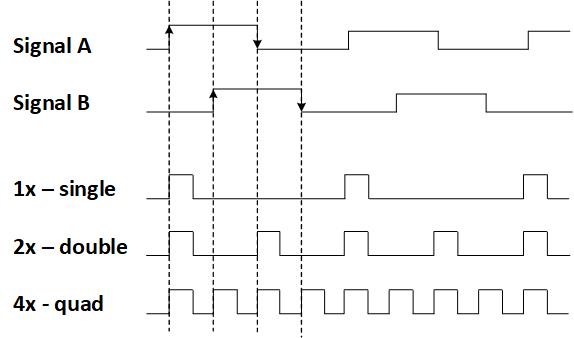
- Quadrature (A-QUAD-B) - Quadrature mode supports standard A and B inputs with optional Index, offering selectable 1x, 2x, or 4x decoding formats to accommodate varying resolution and direction sensing requirements across diverse motion control and position feedback applications.
- General Purpose Counter - Similar to the incremental mode, the general-purpose mode features pre-loadable up/down counters, with the additional capability to be triggered by a programmable internal clock or an external trigger source.
Built-In Test: The EC1 Encoder smart function module features continuous Built-In Test (BIT) functionality that is always enabled to ensure ongoing operational integrity and fault detection. The BIT system performs real-time verification of A, B, and C signal inputs, checking for common interface issues.
- For RS422 inputs, it detects open and short conditions as well as voltage levels outside the nominal operating range. For RS232 inputs, it monitors for out-of-range voltages. This proactive diagnostic capability enhances system reliability and simplifies fault isolation in mission-critical environments.
COSA™ SerDes: The EC1 is fully integrated with NAI’s COSA™ (Configurable Open Systems Architecture), providing seamless interoperability within a modular system environment. It features a high-speed SerDes interface that enables fast, low-latency data transfer between the module and host processor. Additionally, the module supports multi-event interrupt capability, allowing prioritized and responsive handling of multiple encoder events in real time—ideal for time-sensitive applications in defense, aerospace, and industrial automation systems.
PRINCIPLES OF OPERATION
Each module incorporates four (4) independent isolated programmable encoder/counter I/O channels. These encoder/counter channels can interface directly to independent industrial encoders without any concern about groundings. Each channel is programmable as an SSI interface controller, an SSI “Listen Only” mode receiver, an incremental encoder reader or a general-purpose counter.
- When programmed in the SSI controller mode, the channel will output a clock to the encoder and will receive the encoder positional data signal. The SSI controller has a programmable clock rate.
- When programmed in the SSI “Listen Only” mode, the channel will accept both the clock and positional data signal as inputs. The data word can be programmed in binary or gray codes with parity.
- When programmed as a Quadrature encoder counter, the channel can accept an index pulse in conjunction with the A and B signal inputs in 1x, 2x or 4x input format.
- When programmed as an incremental encoder, sub-programming options include pre-loadable up/down counters.
- When programmed as a general-purpose counter, the channels are pre-loadable and can be controlled as an UP or DOWN counter which can be fed via a programmable internal clock source or an external signal trigger.
Channel Inputs
| { Channel Mode | Channel A | Channel B | Index |
| SSI (Standard) | Clock (Out) | Data (In) | N/A |
| SS (Listen Only) | Clock (In) | Data (In) | N/A |
| Timer Mode | N/A | N/A | Control (In) |
| Direction Count | Counter (In) | Counter Direction (In) | Control (In) |
| Up/Down Count | Count (Up) | Count (Down) | Control (In) |
| Quadrature | Input A | Input B | Control (In) |
Note
to set a channel to either SSI or Counter mode, the channel must first be configured, then programmed for either SSI or Counter mode.
SSI Mode
Description
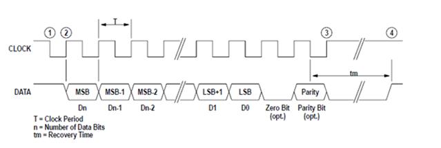
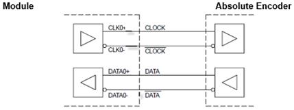
The Synchronous Serial Interface (SSI) is based on two differential signal lines, CLOCK and DATA. The CLOCK line is an input, the DATA line is an output of the absolute encoder.
 SSI Timing Example
When not transmitting, the clock and data lines are high. To read out the positional data of an absolute encoder, the controller transmits a pulse train on the CLOCK line. The first falling edge of CLOCK latches the positional data of the absolute encoder. At the first rising edge of CLOCK the absolute encoder presents the most significant bit on the DATA line. On each subsequent rising edge in the CLOCK pulse train the next bit in order is transmitted to the controller.
In addition to the data bits the absolute encoder can transmit a parity bit for error detection. As an option a zero bit can be placed between the data and the parity bit. After all bits are transmitted, the absolute encoder holds the data line low for 10-30µs (recovery time tm). After that the absolute encoder is ready for a new transmission. A new transmission must not be started before recovery time.
Standard SSI Interface Controller Mode
In this mode A Module channel operates as a standard SSI interface controller. The SSI clock is an output, and the data signal is an input to the module:
This mode is enabled when the Mode Register is set to “01” and the MODE bit in the SSI Config Register is set to (0).
| Register | Name | Setting |
| Mode | SSI (bit 0) | “01” |
| SSI Config register | MODE (bit 24) | “0” |
SSI Standard Mode Selection
In the SSI Config Register the SSI interface must be set up, conforming to the settings required of the connected absolute encoder:
| Register | Name | Setting |
| SSI Config Register | bin.v.gray | Binary Code/Gray Code Data |
| Zero Bit | No Bit/Zero Bit Mode | |
| Parity_oe | Even/Odd Parity | |
| Parity_en | Encoder w/Parity + (No Parity Error or Bit/Parity Error) | |
| Watchdog_En | See SSI Listen Only Mode Selection | |
| Break | See SSI Listen Only Mode Selection | |
| Mode | Standard or Listen Only Mode | |
| Clock Rate | Clock can be programmed in steps of 1 us from 1 to 32; value of 0 will stop SSI Interface operation | |
| Dwell Time | Number of Idled Clock Cycles Between SSI Read Cycles | |
| Data Bits | Actual Number of Data Bits |
A one-time data transfer is initiated by writing a 1 to the SSI Control register (it can also be triggered from the Global Register multichannel read. The SSI interface controller then generates a clock burst, on which the absolute encoder returns its positional data. The SSI Controller receives this data, processes it (parity check, gray-to-binary code conversion) and indicates the end of the data transfer with the de-assertion of the busy bit and setting of the new-data bit. If enabled, an interrupt is asserted, and the positional data can then be read in the Data Register. In this mode the watchdog error status bit is always read zero (0).
Wiring Example: Channel 0, SSI Interface Controller Mode. This mode is enabled when the Mode Register is set to (01) and the MODE bit in the SSI Config Register is set to (0).
Listen Only Mode
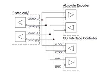
This mode is enabled when the Mode Register is set to “01” and the MODE bit in the SSI Config Register is set to (1).
| Register | Name | Setting |
| Mode | SSI (bit 0) | “01” |
| SSI Config register | MODE (bit 24) | “1” |
SSI Listen Only Mode Selection
In the Control Register the SSI interface must be set up, conforming to the settings required of the observed SSI interface:
| Register | Symbol | Setting |
| SSI Config Register | bin.v.gray | Binary Code/Gray Code Data |
| Zero Bit | No Zero Bit/Zero Bit Mode | |
| Parity_oe | Even/Odd Parity | |
| Parity_en | Encoder w/Parity + (No Parity Error or Bit/Parity Error) | |
| Watchdog En | Watchdog Timer Enabled/Disabled + (Listen Mode Only) | |
| Break | Read Error Ignored/Listen on Read Errors + (Listen Only) | |
| Mode | Standard or Listen Only Mode | |
| Clock Rate | Clock rate setting ignored + (clock rate is detected automatically) | |
| Dwell | Number of Idled Clock Cycles Between SSI Read Cycles | |
| Data Bits | Actual Number of Data Bits |
The clock rate setting in the Control Register is “don’t care”; the clock rate of the observed SSI interface will be detected automatically. After the Control Register is set up, the channel begins listening (indicated by Busy = 1) when either a 1 is written to the SSI Control register or when the Global Register multichannel read is triggered (the multichannel read trigger can also be tied to the interval timer mode).
A data transfer is initiated by the observed SSI interface. The positional data will be received and processed (parity check, gray to binary code conversion) and the end of the data transfer is indicated with the de-assertion of the Busy bit or by setting the new data bit in the status register. If enabled, an interrupt is asserted, and the positional data can be read in the Data Register.
Note
In this mode the clock rate setting in the Control Register is ignored; the Clock Rate will be detected automatically.
In case of a partial transmission a read error will be issued in the Status Register. To detect read errors, the width of the first SSI clock pulse is measured to detect the clock rate. This clock rate is multiplied by 4 and used as the initial value for a watchdog timer. Every new received bit resets the watchdog timer, until either the programmed data word length is reached (successful read) or a timeout occurs (watchdog error).
In case of a timeout the Watchdog Error bit is set to (1) if the Watchdog Enable bit is set. Depending on the BREAK setting in the SSI Config Register the channel ignores a read error and continues listening or it stops to listen. Reasons for a read error are:
- The number of data bits set in the control register does not match the actual size of the received transmission.
- Only a partial transmission was monitored (this could happen when the mode is switched, and a transmission is in progress on the observed SSI interface).
Parity
Parity is the sum of data bits in the SSI word, with the bits high (1).
| SSI Mode | Sum of Input Bits | Even Parity (Par_oe = 0) | Odd Parity (Par_oe = 1) |
| Even Number of 1's | Parity Bit S/b = 1 | Parity Bit S/b = 0 | Odd Number of 1's |
| Parity Bit S/b = 0 | Parity Bit S/b = 1 |
| SSI Mode | Standard SSI Interface Mode | 'Listen only' Mode |
| SSI Config Register | Clock Rate value of 0 will stop SSI Interface. Bit 24 (MODE) is Set to 0 | Clock Rate Setting in SSI Config Register is 'Don't Care'. Bit 24 (MODE) is Set to 1 |
| Status Register | Status Register Busy bit = 1 during transmission | Busy bit = 1 While Channel is Listening |
| Watchdog Error Bit | Watchdog Error Bit is Always 0 | Watchdog Error Bit is Set to 1 on a Erroneous Transmission when the Watchdog_En bit is a 1. |
| Extra Clock Bit | Extra Clock Bit is Always 0 | Extra Clock Bit is Set to 1 When More Falling Edges are Indicated than Programmed for (BC) value. |
| Data Transfer Start | Data Transfer is Initiated by writing a 1 to the SSI Control Register or a Multiple Channel Read | Data Transfer is Initiated by writing a 1 to the SSI Control Register or a Multiple Channel Read. |
Counter Mode
Special Count Modes
In normal operation, the counter is a cycling counter. Two additional special count modes are available. The Count Modes are available for every Input Mode.
Divide-by-N
The counter is enabled in the Control Register and will run until it is disabled. The counter is loaded with the content of the preload register every time the counter creates a borrow or a carry.
Single Cycle
The counter is enabled in the Control Register and will start on the following events:
- A manual preload or reset in the Counter Command Register
- A manual counter preload in the Global Control Register
- A control mode event in .Load on I. or .Reset on I. mode
The counter will stop when it creates a borrow or a carry.
Index Control Modes (ICM)
The Index Control Mode determines how events on the I-input are interpreted. Except for the ‘Gate on I’ and ‘Reset on I’ (except in quad mode), all modes react on an edge change on the I-input.
Note
to read the value of the counter the user must first read the fine real-time counter, which will latch the coarse counter value and place it in the coarse counter value latched register. This register can be ‘latched’ by software or by an external event on the I-input and read later.
Note
‘Load on I’ will load the fine real-time counter; the coarse counter will remain unchanged.
Up/Down Count
The counter acts as up-/down counter. Counting pulses are generated when a transition from low to high of either the A- or the B-input is detected. The A-input counts up, the B-input counts down. Simultaneous transitions on the A- and B-input do not generate a counting pulse.
Quadrature Mode
The counter acts as quadrature counter. A-input is quadrature input A, B-input is quadrature input B.
The quadrature inputs can be interpreted as 1x, 2x or 4x counting. 1x lets the counter count once for each full cycle of the quadrature inputs, 2x lets the counter count once for each half cycle of the quadrature inputs and 4x lets the counter count once for each quarter cycle of the quadrature inputs. The count direction (increase or decrease) is determined by the relative phase of the A- and B-signals.
Multiple Channel Read
Multi-channel read, is used to simultaneously latch the value of two or more SSI encoder channels. The Multiple Channel Read function is enabled through the Global Register. A Multiple Channel Read is triggered by writing 1 to the MCRTR-bit, or alternatively by setting the ITRG bit and enabling the interval timer. When setting the ITRG bit, a Multi-Channel read cycle is triggered each time the interval timer reaches terminal count. To become part of a Multi-channel read group, the MCHRD bit(s) needs to be set 1 for the associated channel.
For Counter modes when using the Multiple Channel Read function, the Multi-Channel read latches the value of the counters that are programmed to be part for the Multi-channel read group. The latched value of counter is available immediately after the trigger occurs.
For SSI modes a Multiple Channel Read trigger starts a conversion for the SSI channels that are part of the group. SSI channels need time for the conversion to complete. To indicate that the data for all the SSI channels that are part of the group is available, the MCRST bit in the Global Register is set to 1. The MCRST remains set, until another Multi-Chanel read is triggered.
Multi-channel Read Data Availability
| SSI Mode |
| MCRST = 0 SSI conversion is in process. New data is not available. |
| MCRST = 1 SSI conversion for channels that are part of the group is complete |
Example: Channels 1-2 are configured for SSI mode, channels 3-4 are configured for counter mode. Channels 1, 3 and 4 are enabled for Multiple Channel Read. A write to the MCRTR bit starts the Multiple Channel Read. Channel 1 starts a conversion and the counter value of channels 3 and 4 are latched. The latched counter value for the enabled counter channels is instantly available and can be read at once. The SSI data is not available until MCRST is set to 1.
Alternatively, an interrupt can be set up for the SSI channel that takes the longest time to complete a conversion. If only counter channels use the multi-channel function, interrupts are not necessary because the counter data is instantly available on MCRTR trigger, or on the Interval Timer terminal count, which has an interrupt.
Debounce, Digital Input Filter
Debounce time can be utilized when channel is selected as an input to “filter” or “ignore” spurious initial transitions. Enter required de-bounce time into appropriate channel registers. Once a signal level is a logic voltage level period longer than the Debounce time, a logic transition is validated. Signal pulse widths less than debounce time are filtered. Once valid, the transition status register flag is set for the channel and the output logic changes state. Enter a value of 0 to disable de-bounce filtering.
Debounce resolution= 40 ns x 2. This results in a minimum resolution of 40 ns (de-bounce LSB=0) and a maximum filter value of (65,534 * 20E-9) or 1.311 msec.
Cycle Time
The Speed register stores time in microseconds (bits 0-30) and direction of the count (bit 31), allowing users to calculate velocity by dividing their know travel distance per cycle by the time measured by the Speed register (with an expected accuracy of 0.1%).
In quadrature counter mode, the EC1 can measure the instantaneous period of the incoming A signal input to enable user calculations of rotational speed. The measurement is based on the high time of the incoming signal and assumes a 50% duty cycle.
Input frequencies below the 1 Hz minimum will return a zero measurement. Recommended frequency range of 1Hz to 10kHz.
The measurement register returns the period in microseconds (bits 0-30), with bit 31 (MSB) indicating the count direction. Direction bit will be 1 for incrementing counts.
Accuracy is reduced with higher frequency signals, +/-5% at 10kHz.
Automatic Background Built-in Test (BIT)/Diagnostic Capability
The module provides an automatic background Built-In-Test (BIT) for each channel. BIT is always enabled and continually checks that each channel is functional except when the chips are being configured.
For TTL: BIT checks for Input voltages that are outside normal operating voltage ranges (below -15V and above +15V).
For RS422: BIT detects faults that include low differential input signals, open-wire, short-circuits and input voltages that are outside normal operating voltage ranges (below -15V and above +15V).
The technique used by the automatic background BIT test consists of an “add-2, subtract-1” counting scheme. BIT will be set approximately 5 ms after a BIT fault is detected. The BIT counter is incremented by 2 when a BIT-fault is detected and decremented by 1 when there is no BIT fault detected and the BIT counter is greater than 0. When the BIT counter exceeds the (programmed) BIT Threshold value, the specific channel’s fault bit in the BIT status register will be set. The “add-2, subtract-1” counting scheme effectively filters momentary or intermittent anomalies by allowing them to “come and go“ before a BIT fault status or indication is flagged. This prevents spurious faults from registering valid such as those caused by EMI and/or dirty power causing false BIT faults. Putting more “weight” on errors (“add-2”) and less “weight” on subsequent passing results (subtract-1) will result in a BIT failure indication even if a channel “oscillates” between a pass and fail state.
Status and Interrupts
The EC1 Function Module provide registers that indicate faults or events. Refer to “Status and Interrupts Module Manual” for the Principle of Operation description.
Module Common Registers
The EC1 Function Module includes module common registers that provide access to module-level bare metal/FPGA revisions & compile times, unique serial number information, and temperature monitoring. Refer to “Module Common Registers Module Manual” for the detailed information.
REGISTER DESCRIPTIONS
The register descriptions provide the register name, Function Address Offset, Type, Data Range, Read or Write information, Initialized Value, a description of the function and, in most cases, a data table.
Standard Channel Registers
Mode
| Function: | Determines SSI Mode vs Counter mode. |
|---|---|
| Type: | unsigned binary word (32-bit) |
| Data Range: | See table |
| Read/Write: | R/W |
| Initialized Value: | 0 |
| Operational Settings: | Setting based on the following table. |
Note
Only one mode should be enabled at a time. Enabling both modes simultaneously will disable channel operation.
| D31 | D30 | D29 | D28 | D27 | D26 | D25 | D24 | D23 | D22 | D21 | D20 | D19 | D18 | D17 | D16 |
| 0 | 0 | 0 | 0 | 0 | 0 | 0 | 0 | 0 | 0 | 0 | 0 | 0 | 0 | 0 | 0 |
| D15 | D14 | D13 | D12 | D11 | D10 | D9 | D8 | D7 | D6 | D5 | D4 | D3 | D2 | D1 | D0 |
| 0 | 0 | 0 | 0 | 0 | 0 | 0 | 0 | 0 | 0 | 0 | 0 | 0 | 0 | Counter | SSI |
| Mode Register Bit Descriptions | ||
| Bit(s) | Name | Description |
| D31:D2 | Reserved | Set Reserved bits to 0. |
| D1 | Counter | Counter mode |
| D0 | SSI | SSI mode |
Note
Only one mode should be enabled at a time. Enabling both modes simultaneously will disable channel operation.
Interface Levels
| Function: | Determines the interface levels for each channel. |
|---|---|
| Type: | unsigned binary word (32-bit) |
| Data Range: | See table |
| Read/Write: | R/W |
| Initialized Value: | 1 |
| Operational Settings: | Setting based on the following table. |
| D31 | D30 | D29 | D28 | D27 | D26 | D25 | D24 | D23 | D22 | D21 | D20 | D19 | D18 | D17 | D16 |
| 0 | 0 | 0 | 0 | 0 | 0 | 0 | 0 | 0 | 0 | 0 | 0 | 0 | 0 | 0 | 0 |
| D15 | D14 | D13 | D12 | D11 | D10 | D9 | D8 | D7 | D6 | D5 | D4 | D3 | D2 | D1 | D0 |
| 0 | 0 | 0 | 0 | 0 | 0 | 0 | 0 | 0 | 0 | 0 | 0 | 0 | 0 | RS-422 | TTL |
| Config Register Bit Descriptions | ||
| Bit(s) | Name | Description |
| D31:D2 | Reserved | Set Reserved bits to 0. |
| D1 | RS-422 | Differential RS-422 mode |
| D0 | TTL | Single-ended TTL mode |
Interval Timer Preload
| Function: | Preload value for the interval timer mode. |
|---|---|
| Type: | unsigned binary word (32-bit) |
| Data Range: | 0x0000 0000 to 0x0000 FFFF |
| Read/Write: | R/W |
| Initialized Value: | 0 |
| D31 | D30 | D29 | D28 | D27 | D26 | D25 | D24 | D23 | D22 | D21 | D20 | D19 | D18 | D17 | D16 |
| 0 | 0 | 0 | 0 | 0 | 0 | 0 | 0 | 0 | 0 | 0 | 0 | 0 | 0 | 0 | 0 |
| D15 | D14 | D13 | D12 | D11 | D10 | D9 | D8 | D7 | D6 | D5 | D4 | D3 | D2 | D1 | D0 |
| D | D | D | D | D | D | D | D | D | D | D | D | D | D | D | D |
Interval Timer Control
| Function: | Clock rate and enable for the interval timer mode. |
|---|---|
| Type: | unsigned binary word (32-bit) |
| Data Range: | See table |
| Read/Write: | R/W |
| Initialized Value: | 0 |
| Operational Settings: | Setting based on the following table. |
| D31 | D30 | D29 | D28 | D27 | D26 | D25 | D24 | D23 | D22 | D21 | D20 | D19 | D18 | D17 | D16 |
| 0 | 0 | 0 | 0 | 0 | 0 | 0 | 0 | 0 | 0 | 0 | 0 | 0 | 0 | 0 | 0 |
| D15 | D14 | D13 | D12 | D11 | D10 | D9 | D8 | D7 | D6 | D5 | D4 | D3 | D2 | D1 | D0 |
| 0 | 0 | 0 | 0 | 0 | 0 | 0 | 0 | 0 | 0 | 0 | 0 | 0 | ITDIV | ITDIV | ITEN |
| Interval Timer Control Register Bit Descriptions | ||
| Bit(s) | Name | Description |
| D31:D3 | Reserved | Set Reserved bits to 0. |
| D2:D1 | ITDIV | Pre-scale value (0:0) 25 MHz - 40 ns ` (0:1) 12.5 MHz - 80 ns ` (1:0) 6.25 MHz - 160 ns + (1:1) 3.125 MHz - 320 ns |
| D0 | ITEN | Interval Timer Enable 0 = Disables the Interval Timer + 1 = Enables the Interval Timer |
Global Register
| Function: | Controls all four channels at once. |
|---|---|
| Type: | unsigned binary word (32-bit) |
| Data Range: | See table |
| Read/Write: | W |
| Initialized Value: | 0 |
| Operational Settings: | Setting based on the following table. |
| D31 | D30 | D29 | D28 | D27 | D26 | D25 | D24 | D23 | D22 | D21 | D20 | D19 | D18 | D17 | D16 |
| 0 | 0 | 0 | 0 | 0 | 0 | 0 | 0 | 0 | 0 | 0 | 0 | 0 | 0 | 0 | 0 |
| D15 | D14 | D13 | D12 | D11 | D10 | D9 | D8 | D7 | D6 | D5 | D4 | D3 | D2 | D1 | D0 |
| 0 | 0 | 0 | 0 | 0 | MCRST | MCRTR | ITGR | CH4 MCRD | CH3 MCRD | CH2 MCRD | CH1 MCRD | CH4 PRELOAD | CH3 PRELOAD | CH2 PRELOAD | CH1 PRELOAD |
| Global Register Bit Descriptions | ||
| Bit(s) | Name | Description |
| D31:D11 | Reserved | Set Reserved bits to 0. |
| D10 | MCRST | Multiple Channel Read Status This bit indicates pending Multiple Channel Read data. When an SSI channel is enabled for Multiple Channel Read, it takes time for the conversion to complete. While in SSI Mode, the channel will wait for the data to be ready before the bit is set to 1. This bit indicates that the conversions of all enabled channels is complete. It will remain set to 1 until the next multiple channel trigger. 1 = Multiple Channel Read Data is valid (for all enabled channels). |
| D9 | MCRTR | Multiple Channel Read Trigger Write a 1 to this bit to trigger a Multiple Channel Read. |
| D8 | ITGR | Interval Timer Trigger 0 = Disables the Interval Timer as trigger for multiple channel read. + 1 = Enables the Interval Timer as trigger for multiple channel read. |
| D7:D4 | CHx_MCRD | Enable Multiple Channel Read Channel (x) 0 = Disables Multiple Channel Read + 1 = Enables Multiple Channel Read |
| D3:D0 | CHx_PRELOAD | Manual Counter Preload Channel (x) Writing a 1 to this bit issues a preload of the corresponding counter with the value of the Counter Preload Register. This preload method is can be used in a Non Reference Mode. Before using this preload method, the corresponding Counter Preload Registers must be loaded with valid data. |
Common Configuration Operation Registers
Termination
| Function: | Determines the termination settings for each channel. |
|---|---|
| Type: | unsigned binary word (32-bit) |
| Data Range: | See table |
| Read/Write: | R/W |
| Initialized Value: | 0 |
| Operational Settings: | Setting based on the following table. |
| D31 | D30 | D29 | D28 | D27 | D26 | D25 | D24 | D23 | D22 | D21 | D20 | D19 | D18 | D17 | D16 |
| 0 | 0 | 0 | 0 | 0 | 0 | 0 | 0 | 0 | 0 | 0 | 0 | 0 | 0 | 0 | 0 |
| D15 | D14 | D13 | D12 | D11 | D10 | D9 | D8 | D7 | D6 | D5 | D4 | D3 | D2 | D1 | D0 |
| 0 | 0 | 0 | 0 | 0 | 0 | 0 | 0 | 0 | 0 | 0 | 0 | 0 | 0 | SE-PullUp | DIFF |
| Termination Register Bit Descriptions | ||
| Bit(s) | Name | Description |
| D31:D2 | Reserved | Set Reserved bits to 0. |
| D1 | SE PullUp | Single-Ended Mode This bit enables or disables a 1K ohm pull-up resistor to the internal 5V rail to support open-collector input signals: 0 = Pull-Up Disabled (Default) + 1 = Pull-Up Enabled |
| D0 | DIFF | Differential Mode This bit enables or disables the differential input termination resistor. This is a 240-ohm (nominal) termination: 0 = Termination Disabled (Default) + 1 = Termination Enabled |
Debounce Value A/B/Index
| Function: | Sets the time period an input signal must be stable when a channel is selected as an input to filter (ignore) spurious initial transitions. |
|---|---|
| Type: | unsigned binary word (32-bit) |
| Data Range: | 0x0000 0000 to 0x0000 FFFF |
| Read/Write: | R/W |
| Initialized Value: | 0 |
| D31 | D30 | D29 | D28 | D27 | D26 | D25 | D24 | D23 | D22 | D21 | D20 | D19 | D18 | D17 | D16 |
| 0 | 0 | 0 | 0 | 0 | 0 | 0 | 0 | 0 | 0 | 0 | 0 | 0 | 0 | 0 | 0 |
| D15 | D14 | D13 | D12 | D11 | D10 | D9 | D8 | D7 | D6 | D5 | D4 | D3 | D2 | D1 | D0 |
| D | D | D | D | D | D | D | D | D | D | D | D | D | D | D | D |
Debounce Enable
| Function: | Determines whether debounce circuit is disabled or if input signal is filtered. |
|---|---|
| Type: | unsigned binary word (32-bit) |
| Data Range: | See table |
| Read/Write: | R/W |
| Initialized Value: | 0 |
| Operational Settings: | Setting based on the following table. |
| D31 | D30 | D29 | D28 | D27 | D26 | D25 | D24 | D23 | D22 | D21 | D20 | D19 | D18 | D17 | D16 |
| 0 | 0 | 0 | 0 | 0 | 0 | 0 | 0 | 0 | 0 | 0 | 0 | 0 | 0 | 0 | 0 |
| D15 | D14 | D13 | D12 | D11 | D10 | D9 | D8 | D7 | D6 | D5 | D4 | D3 | D2 | D1 | D0 |
| 0 | 0 | 0 | 0 | 0 | 0 | 0 | 0 | 0 | 0 | 0 | 0 | 0 | By-pass C | By-pass B | By-pass A |
| Debounce Enable Register Bit Descriptions | ||
| Bit(s) | Name | Description |
| D31:D3 | Reserved | Set Reserved bits to 0. |
| D2:D0 | By-pass (x) | Bypass input (x) 0 = Debounce Circuit Bypassed (Disabled) + 1 = The input signal is filtered according to the filter counter value. |
Counter Interface Function Registers
Counter Preload
| Function: | Preloads the counter with this value. |
|---|---|
| Type: | unsigned binary word (32-bit) |
| Data Range: | 0x0000 0000 to 0xFFFF FFFF |
| Read/Write: | R/W |
| Initialized Value: | 0 |
| D31 | D30 | D29 | D28 | D27 | D26 | D25 | D24 | D23 | D22 | D21 | D20 | D19 | D18 | D17 | D16 |
| D | D | D | D | D | D | D | D | D | D | D | D | D | D | D | D |
| D15 | D14 | D13 | D12 | D11 | D10 | D9 | D8 | D7 | D6 | D5 | D4 | D3 | D2 | D1 | D0 |
| D | D | D | D | D | D | D | D | D | D | D | D | D | D | D | D |
Counter Control
| Function: | Controls the counter load and resets. |
|---|---|
| Type: | unsigned binary word (32-bit) |
| Data Range: | 0 or 1; 2 or 4 |
| Read/Write: | R/W |
| Initialized Value: | 0 |
| Operational Settings: | Set bit D0 to 1 to reset the counter. Set bit D1 to 1 to load the counter. Set bit D2 to 1 to latch the counter values. |
| D31 | D30 | D29 | D28 | D27 | D26 | D25 | D24 | D23 | D22 | D21 | D20 | D19 | D18 | D17 | D16 |
| 0 | 0 | 0 | 0 | 0 | 0 | 0 | 0 | 0 | 0 | 0 | 0 | 0 | 0 | 0 | 0 |
| D15 | D14 | D13 | D12 | D11 | D10 | D9 | D8 | D7 | D6 | D5 | D4 | D3 | D2 | D1 | D0 |
| 0 | 0 | 0 | 0 | 0 | 0 | 0 | 0 | 0 | 0 | 0 | 0 | 0 | Latch Counter | Load counter | Reset counter |
Counter Config
| Function: | Configures the inputs and the counter. |
|---|---|
| Type: | unsigned binary word (32-bit) |
| Data Range: | See table |
| Read/Write: | R/W |
| Initialized Value: | 0 |
| Operational Settings: | Setting based on the following tables. |
| D31 | D30 | D29 | D28 | D27 | D26 | D25 | D24 | D23 | D22 | D21 | D20 | D19 | D18 | D17 | D16 |
| compare enable | 0 | 0 | 0 | 0 | 0 | 0 | 0 | 0 | 0 | 0 | 0 | 0 | POL2 | POL1 | POL0 |
| D15 | D14 | D13 | D12 | D11 | D10 | D9 | D8 | D7 | D6 | D5 | D4 | D3 | D2 | D1 | D0 |
| 0 | 0 | CLK_DIV1 | CLK_DIV0 | 0 | CIM2 | CIM1 | CIM0 | 0 | 0 | SCM1 | SCM0 | 0 | ICM2 | ICM1 | ICM0 |
| Counter Config Register Bit Descriptions | ||
| Bit(s) | Name | Description |
| D31 | Compare enable | Enables Counter Compare register 0 = Counter Compare disabled + 1 = Counter Compare enabled. The interrupt will be set if the value in the Counter Compare register is equal to the fine counter realtime value. |
| D30:D19 | Reserved | Set Reserved bits to 0. |
| D18:D16 | POL (x) | Polarity (x) |
| D15:D14 | Reserved | Set Reserved bits to 0. |
| D13:D12 | CLK_DIV (x) | Clock Divide (x) |
| D11 | Reserved | Set Reserved bits to 0. |
| D10:D8 | CIM (x) | Counter Input Mode (x) |
| D7:D6 | Reserved | Set Reserved bits to 0. |
| D5:D4 | SCM (x) | Special Count Mode (x) |
| D3 | Reserved | Set Reserved bits to 0. |
| D2:D0 | ICM (x) | Index Count Mode (x) |
| Index Control Modes | ||||
| ICM[2:0] | Name | POL = 0 | POL = 1 | Description |
| 0:0:0 | Ignore I-Input | Rising Edge | Falling Edge | I-Input is ignored. |
| 0:0:1 | Load On I | Rising Edge | Falling Edge | An event on the I-input loads the counter with the content of the Counter Preload Register. If the 'Single Cycle' mode is active, the event on the I-input will start the counter. This control mode can be used to establish a known reference position in a mechanical system. |
| 0:1:0 | Latch On I | Rising Edge | Falling Edge | An event on the I-input loads and locks the Counter Latch Register with the counter value. This register remains latched until a new event I input event reloads this register. This control mode can be used to capture a position in a mechanical system. |
| 0:1:1 | Gate On I | Level High | Level Low | The signal level on the I-input enables or disables counting. Remember that in this mode the I-input is level sensitive. 0 = Counter Disabled + 1 = Counter Enabled When a signal with constant frequency is connected to the A- and B-inputs, this control mode can be used for impulse width measurements. |
| 1:0:0 | Reset On I | Level High | Level Low | An event on the I-input resets (clears) the counter. The counter can also be reset by writing '1' to the 'Reset Counter' (RCNT) bit in the Counter Command Register. This control mode can be used to establish a known home or reference position in a mechanical system. NOTE: Quadrature mode is edge sensitive, not level sensitive. |
| 1:0:1 | Ignore I-Input | - | - | I-Input is ignored. |
| 1:1:0 | Ignore I-Input | - | - | I-Input is ignored. |
| 1:1:1 | Ignore I-Input | - | - | I-Input is ignored. |
| Special Count Modes | ||
| SCM[1:0] | Name | Description |
| 0:0 | No special mode | Normal operation: counter is a cycling counter. |
| 0:1 | Divided-by-N | The counter is enabled in the Counter Config Register and will run until it is disabled. The counter is loaded with the content of the preload register every time the counter creates a borrow or a carry. |
| 1:0 | Single Cycle | The counter is enabled in the Counter Config Register and will start on following events: • A manual preload or reset in the Counter Command Register ` • A manual counter preload in the Global Control Register ` • A control mode event in Load on I or Reset on I mode The counter will stop when it creates a borrow or a carry. |
| Counter Input Modes | |||||
| CIM[2:0] | Name | Counter Input Source | A Input | B Input | Description |
| 0:0:0 | Counter Disabled | - | - | The counter is disabled. | |
| 0:0:1 | Timer Mode Up | Internal Clock Prescaler | - | - | In Timer mode the counter uses an internal clock pre-scaler as input. |
| 0:1:0 | Timer Mode Down | Internal Clock Prescaler | - | - | In Timer mode the counter uses an internal clock pre-scaler as input. |
| 0:1:1 | Direction Count | Input A & Input B | Count | Count Direction Up/Down | The counter acts as up/down counter. Counting pulses are generated when a transition from low to high of the A-input is detected. The B-input determines the count direction: 0 = Down + 1 = Up |
| 1:0:0 | Up/Down Count | Input A & Input B | Count Up | Count Down | The counter acts as up-/down counter. Counting pulses are generated when a transition from low to high of either the A- or the B-input is detected. The A-input counts up, the B-input counts down. Simultaneous transitions on the A- and B-input do not generate a counting pulse. |
| 1:0:1 | Quadrature Count x1 | Input A & Input B | Quadrature A | Quadrature B | The counter acts as quadrature counter. A-input is quadrature input A, B-input is quadrature input B. The quadrature inputs can be interpreted as 1x, 2x or 4x counting. 1x lets the counter count once for each full cycle of the quadrature inputs, 2x lets the counter count once for each half cycle of the quadrature inputs and 4x lets the counter count once for each quarter cycle of the quadrature inputs. The count direction (increase or decrease) is determined by the relative phase of the A- and B-signals.  |
| 1:1:0 | Quadrature Count x2 | Input A & Input B | Quadrature A | Quadrature B | |
| 1:1:1 | Quadrature Count x4 | Input A & Input B | Quadrature A | Quadrature B | |
| Clock Divide Frequencies++``+ | ||
| CLK_DIV[1:0] | Divide by | Clock Frequency |
| 0:0 | 1 | 62.5 MHz |
| 0:1 | 2 | 25 MHz |
| 1:0 | 4 | 12.5 MHz |
| 1:1 | 8 | 6.25 MHz |
| Polarity Inputs | |||
| POL[2:0] | Input | POL = 0 | POL = 1 |
| POL[2] | INDEX | Rising Edge* | Falling Edge |
| POL[1] | B | Rising Edge | Falling Edge |
| POL[0] | A | Rising Edge | Falling Edge |
*except for ‘Gate on I’ and ‘Reset on I’ in Quadrature Mode
Coarse Counter Latched
| Function: | Latched value of the coarse counter. |
|---|---|
| Type: | unsigned binary word (32-bit) |
| Data Range: | 0x0000 0000 to 0xFFFF FFFF |
| Read/Write: | R |
| Initialized Value: | 0 |
| D31 | D30 | D29 | D28 | D27 | D26 | D25 | D24 | D23 | D22 | D21 | D20 | D19 | D18 | D17 | D16 |
| D | D | D | D | D | D | D | D | D | D | D | D | D | D | D | D |
| D15 | D14 | D13 | D12 | D11 | D10 | D9 | D8 | D7 | D6 | D5 | D4 | D3 | D2 | D1 | D0 |
| D | D | D | D | D | D | D | D | D | D | D | D | D | D | D | D |
Coarse Counter Realtime
| Function: | Realtime value of the coarse counter. |
|---|---|
| Type: | unsigned binary word (32-bit) |
| Data Range: | 0x0000 0000 to 0xFFFF FFFF |
| Read/Write: | R |
| Initialized Value: | 0 |
| D31 | D30 | D29 | D28 | D27 | D26 | D25 | D24 | D23 | D22 | D21 | D20 | D19 | D18 | D17 | D16 |
| D | D | D | D | D | D | D | D | D | D | D | D | D | D | D | D |
| D15 | D14 | D13 | D12 | D11 | D10 | D9 | D8 | D7 | D6 | D5 | D4 | D3 | D2 | D1 | D0 |
| D | D | D | D | D | D | D | D | D | D | D | D | D | D | D | D |
Fine Counter Latched
| Function: | Latched value of the fine counter. |
|---|---|
| Type: | unsigned binary word (32-bit) |
| Data Range: | 0x0000 0000 to 0xFFFF FFFF |
| Read/Write: | R |
| Initialized Value: | 0 |
| D31 | D30 | D29 | D28 | D27 | D26 | D25 | D24 | D23 | D22 | D21 | D20 | D19 | D18 | D17 | D16 |
| D | D | D | D | D | D | D | D | D | D | D | D | D | D | D | D |
| D15 | D14 | D13 | D12 | D11 | D10 | D9 | D8 | D7 | D6 | D5 | D4 | D3 | D2 | D1 | D0 |
| D | D | D | D | D | D | D | D | D | D | D | D | D | D | D | D |
Fine Counter Realtime
| Function: | Realtime value of the fine counter. |
|---|---|
| Type: | unsigned binary word (32-bit) |
| Data Range: | 0x0000 0000 to 0xFFFF FFFF |
| Read/Write: | R |
| Initialized Value: | 0 |
| D31 | D30 | D29 | D28 | D27 | D26 | D25 | D24 | D23 | D22 | D21 | D20 | D19 | D18 | D17 | D16 |
| D | D | D | D | D | D | D | D | D | D | D | D | D | D | D | D |
| D15 | D14 | D13 | D12 | D11 | D10 | D9 | D8 | D7 | D6 | D5 | D4 | D3 | D2 | D1 | D0 |
| D | D | D | D | D | D | D | D | D | D | D | D | D | D | D | D |
Counter Compare
| Function: | Sets match flag in the counter status register when fine counter Realtime value is equal to counter compare value. |
|---|---|
| Type: | unsigned binary word (32-bit) |
| Data Range: | 0x0000 0000 to 0xFFFF FFFF |
| Read/Write: | R/W |
| Initialized Value: | 0 |
| D31 | D30 | D29 | D28 | D27 | D26 | D25 | D24 | D23 | D22 | D21 | D20 | D19 | D18 | D17 | D16 |
| D | D | D | D | D | D | D | D | D | D | D | D | D | D | D | D |
| D15 | D14 | D13 | D12 | D11 | D10 | D9 | D8 | D7 | D6 | D5 | D4 | D3 | D2 | D1 | D0 |
| D | D | D | D | D | D | D | D | D | D | D | D | D | D | D | D |
SSI Interface Controller/Listener Function Registers
SSI Data
| Function: | Received SSI data registers. |
|---|---|
| Type: | unsigned binary word (32-bit) |
| Data Range: | 0x0000 0000 to 0xFFFF FFFF |
| Read/Write: | R |
| Initialized Value: | 0 |
| D31 | D30 | D29 | D28 | D27 | D26 | D25 | D24 | D23 | D22 | D21 | D20 | D19 | D18 | D17 | D16 |
| D | D | D | D | D | D | D | D | D | D | D | D | D | D | D | D |
| D15 | D14 | D13 | D12 | D11 | D10 | D9 | D8 | D7 | D6 | D5 | D4 | D3 | D2 | D1 | D0 |
| D | D | D | D | D | D | D | D | D | D | D | D | D | D | D | D |
SSI Control
| Function: | Controls the SSI reads. |
|---|---|
| Type: | unsigned binary word (32-bit) |
| Data Range: | 0 or 1 |
| Read/Write: | W |
| Initialized Value: | 0 |
| Operational Settings: | Write a 0 to disable SSI reads; write a 1 to trigger one-time SSI read. |
| D31 | D30 | D29 | D28 | D27 | D26 | D25 | D24 | D23 | D22 | D21 | D20 | D19 | D18 | D17 | D16 |
| 0 | 0 | 0 | 0 | 0 | 0 | 0 | 0 | 0 | 0 | 0 | 0 | 0 | 0 | 0 | 0 |
| D15 | D14 | D13 | D12 | D11 | D10 | D9 | D8 | D7 | D6 | D5 | D4 | D3 | D2 | D1 | D0 |
| 0 | 0 | 0 | 0 | 0 | 0 | 0 | 0 | 0 | 0 | 0 | 0 | 0 | 0 | 0 | Read |
SSI Config
| Function: | Configures the SSI settings. |
|---|---|
| Type: | unsigned binary word (32-bit) |
| Data Range: | See table |
| Read/Write: | R/W |
| Initialized Value: | 0 |
| Operational Settings: | See bit descriptions table. |
| D31 | D30 | D29 | D28 | D27 | D26 | D25 | D24 | D23 | D22 | D21 | D20 | D19 | D18 | D17 | D16 |
| bin.v.gray | Zero bit | Parity_oe | Parity_en | Watchdog_en | 0 | Break | Mode | 0 | 0 | Clock Rate | Clock Rate | Clock Rate | Clock Rate | Clock Rate | Clock Rate |
| D15 | D14 | D13 | D12 | D11 | D10 | D9 | D8 | D7 | D6 | D5 | D4 | D3 | D2 | D1 | D0 |
| 0 | 0 | 0 | Dwell Time | Dwell Time | Dwell Time | Dwell Time | Dwell Time | 0 | 0 | 0 | D | D | D | D | D |
| SSI Config Bit Descriptions | ||
| Bit(s) | Name | Description |
| D31 | bin.v.gray | Gray to binary code conversion 0 = Binary Code Data + 1 = Gray Code Data |
| D30 | Zero Bit | 0 = No Bit Mode + 1 = Zero Bit Mode |
| D29 | Par_Oe | 0 = Even Parity + 1 = Odd Parity |
| D28 | Par_En | Encoder with Parity - If Encoder provides a parity bit: 0 = No Parity Errors / No Parity Bit + 1 = Parity Errors |
| D27 | Watchdog_En | Watchdog Timer Enable (Listen Only) 0 = Disabled + 1 = Enabled Once enabled, this bit will check for any read errors in data (ex: loss of clock, partial transmission) |
| D26 | Reserved | Set Reserved bits to 0. |
| D25 | Break | Break on Read Error (Listen Only) 0 = Read Errors are ignored and the channel resumes to listen. + 1 = The channel stops to listen on read errors. |
| D24 | Mode | 0 = Standard Mode + 1 = SSI Listen only |
| D23:D22 | Reserved | Set Reserved bits to 0. |
| D21:D16 | Clock Rate | Clock rate for encoder serial clock speed. The clock can be programmed in steps of 1 us in the range of 1 to 32. A value of 0 for the clock rate will stop the operation of the SSI Interface. The Listen-only Mode will ignore the Clock Rate setting; in this mode, the Clock Range will be detected automatically. |
| D15:D13 | Reserved | Set Reserved bits to 0. |
| D12:D8 | Dwell Time | Number of bit cycle that the clock idles for after an SSI read. |
| D7:D6 | Reserved | Set Reserved bits to 0. |
| D5:D0 | Data Bits | Actual number of data bits. (x20 Max) |
SSI ZB/Par
| Function: | Displays the zero bit and parity from the encoder. |
|---|---|
| Type: | unsigned binary word (32-bit) |
| Data Range: | See table |
| Read/Write: | R |
| Initialized Value: | 0 |
| Operational Settings: | Setting based on the following table. |
| D31 | D30 | D29 | D28 | D27 | D26 | D25 | D24 | D23 | D22 | D21 | D20 | D19 | D18 | D17 | D16 |
| 0 | 0 | 0 | 0 | 0 | 0 | 0 | 0 | 0 | 0 | 0 | 0 | 0 | 0 | 0 | 0 |
| D15 | D14 | D13 | D12 | D11 | D10 | D9 | D8 | D7 | D6 | D5 | D4 | D3 | D2 | D1 | D0 |
| 0 | 0 | 0 | 0 | 0 | 0 | 0 | 0 | 0 | 0 | 0 | 0 | 0 | 0 | ZB | Parity |
| SI ZB/Par Bit Descriptions | ||
| Bit(s) | Name | Description |
| D31:D2 | Reserved | Set Reserved bits to 0. |
| D1 | ZB | Displayed zero bit (should be zero) |
| D0 | Parity | Displayed parity bit |
Speed Register
| Function: | Calculates the time between rising edges for frequency which can be used to calculate speed. Valid in Counter mode only. |
|---|---|
| Type: | unsigned binary word (32-bit) |
| Data Range: | See table |
| Read/Write: | R |
| Initialized Value: | 0 |
| Operational Settings: | Setting based on the following table. |
| D31 | D30 | D29 | D28 | D27 | D26 | D25 | D24 | D23 | D22 | D21 | D20 | D19 | D18 | D17 | D16 |
| Direction | D | D | D | D | D | D | D | D | D | D | D | D | D | D | D |
| D15 | D14 | D13 | D12 | D11 | D10 | D9 | D8 | D7 | D6 | D5 | D4 | D3 | D2 | D1 | D0 |
| D | D | D | D | D | D | D | D | D | D | D | D | D | D | D | D |
| Speed Bit Descriptions | ||
| Bit(s) | Name | Description |
| D31 | Count Direction | 1 = Count Up + 0 = Count Down |
| D30:D0 | Data Bits | Time (in µs) from rising edge to rising edge |
Module Common Registers
Refer to ‘Module Common Registers Module Manual’ for the register descriptions.
Status and Interrupt Registers
The EC1 Module provides registers for BIT and EC1 status.
BIT Status
There are four registers associated with the BIT Status: Dynamic Status, Latched Status, Interrupt Enable, and Set Edge/Level Interrupt.
| Function: | Sets the corresponding bit associated with the channel’s BIT error. |
|---|---|
| Type: | unsigned binary word (32-bits) |
| Data Range: | 0x0000 0000 to 0x0000 000F |
| Read/Write: | R (Dynamic), R/W (Latched, Interrupt Enable, Edge/Level Interrupt) |
| Initialized Value: | 0 |
| BIT Dynamic Status Register | |||||||||||||||
| BIT Latched Status Register | |||||||||||||||
| BIT Interrupt Enable Register | |||||||||||||||
| BIT Set Edge/Level Interrupt Register | |||||||||||||||
| D31 | D30 | D29 | D28 | D27 | D26 | D25 | D24 | D23 | D22 | D21 | D20 | D19 | D18 | D17 | D16 |
| 0 | 0 | 0 | 0 | 0 | 0 | 0 | 0 | 0 | 0 | 0 | 0 | 0 | 0 | 0 | 0 |
| D15 | D14 | D13 | D12 | D11 | D10 | D9 | D8 | D7 | D6 | D5 | D4 | D3 | D2 | D1 | D0 |
| 0 | 0 | 0 | 0 | 0 | 0 | 0 | 0 | 0 | 0 | 0 | 0 | Ch4 | Ch3 | Ch2 | Ch1 |
EC1 Status
There are four registers associated with the EC1 Status: Dynamic Status, Latched Status, Interrupt Enable, and Set Edge/Level Interrupt.
| Function: | Sets the corresponding bit associated with each event type. |
|---|---|
| Type: | unsigned binary word (32-bits) |
| Data Range: | See table |
| Read/Write: | R (Dynamic), R/W (Latched, Interrupt Enable, Edge/Level Interrupt) |
| Initialized Value: | 0 |
| EC1 Dynamic Status Register | |||||||||||||||
| EC1 Latched Status Register | |||||||||||||||
| EC1 Interrupt Enable Register | |||||||||||||||
| EC1 Set Edge/Level Interrupt Register | |||||||||||||||
| D31 | D30 | D29 | D28 | D27 | D26 | D25 | D24 | D23 | D22 | D21 | D20 | D19 | D18 | D17 | D16 |
| 0 | 0 | 0 | 0 | 0 | 0 | 0 | 0 | 0 | 0 | 0 | 0 | 0 | 0 | 0 | 0 |
| D15 | D14 | D13 | D12 | D11 | D10 | D9 | D8 | D7 | D6 | D5 | D4 | D3 | D2 | D1 | D0 |
| 0 | Extra | WD_error | p-err | Busy | zero_bit_err | Overflow | new-data | 0 | 0 | SGL | DIR | SGN | MAT | CRY | BOR |
| EC1 Status Bit Descriptions | ||
| Bit(s) | Name | Description |
| D31:D15 | Reserved | Set Reserved bits to 0. |
| D14 | Extra | EXTRA Valid only in 'Listen Only' Mode. 1 = Indicates more Falling Edges of the SSI Clock than programmed for the (BC) value. Will look for an extra clock for one period after the data is ready. |
| D13 | WD_error | Watch Dog Error Valid only in 'Listen Only' Mode. 1 = SSI Watch Dog Timer Error. This bit is set if the watch dog timer times out. (SSI_CLK) stalls before the (BC) number of bits are received. Clock period and SSI clock are calculated and multiplied by 4 to set timeout value. If a clock is not received within that timeframe, channel will either break or keep listening based on break bit in Config register. Watchdog Enable bit in Config register MUST be set for this bit to work. |
| D12 | p-err | Encoder with Parity - If Encoder provides a parity bit: 0 = No Parity Errors / No Parity Bit + 1 = Parity Error |
| D11 | Busy | Busy bit In Standard SSI Interface Controller Mode 1 = Indicates a transmission in progress (Busy bit sourced from the baud rate generator) In 'Listen Only' Mode 1 = Indicates that channel is listening, and transmission can take place later after channel is listening; transmission does not need to be in process. (Busy bit sourced from the SSI watch dog timer) |
| D10 | Zero_bit_err | Zero bit error In Standard SSI Interface Controller Mode 0 = No Zero bit error ` 1 = Zero bit error NOTE: In this mode status will be set if Zero bit is Config register is enabled and this bit receives a 1 instead of a 0. In 'Listen Only' Mode 0 = No Zero bit error ` 1 = Zero bit error |
| D9 | Overflow | Overflow In 'Standard SSI Interface Controller' Mode 1 = Overflow flag. In 'Listen Only' Mode 1 = Overflow flag. NOTE: This bit is set if data is ready when new data is set. The data register will be updated with the new value. |
| D8 | New-data | New Data In 'Standard SSI Interface Controller' Mode 1 = New Data Ready. This bit is set after a successful cycle of the controller of listen and clears when the data is read. In 'Listen Only' Mode 1 = New Data Ready. This bit is set after a successful cycle of the controller of listen and clears when the data is read. |
| D7:D6 | Reserved | Set Reserved bits to 0. |
| D5 | SGL | Single Cycle Active In Single Cycle counting mode this bit is set to 1 when the counter is active. It is reset to 0 when the counter has counted down to zero. Will also reset to zero if the counter has counted up to FFFF FFFF. |
| D4 | DIR | Count Direction This bit indicates the counting direction of the counter. 1 = up + 0 = down In the 'Up/Down Count' mode this bit indicates the direction at the last count. In the 'Direction Count' Mode this bit corresponds to the B-input. |
| D3 | SGN | Sign This bit is set to 1 when the counter overflows and is set to 0 when the counter underflows. After reset or power-up this bit should be considered as 'don't care' until the first Carry or Borrow occurs. |
| D2 | MAT | Match This bit is set to 1 when the fine counter realtime value matches the value of the Counter Compare Register. |
| D1 | CRY | Carry This bit is set to 1 when the counter changes from 0xFFFF FFFF to 0x0000 0000. |
| D0 | BOR | Borrow This bit is set to 1 when the counter changes from 0x0000 0000 to 0xFFFF FFFF. |
FUNCTION REGISTER MAP
KEY
| Configuration/Control |
| Measurement/Status |
| STANDARD CONTROL REGISTERS | |||||
| OFFSET | REGISTER NAME | ACCESS | OFFSET | REGISTER NAME | ACCESS |
| 0x110C | Mode Ch.1 | R/W | 0x1100 | Interface Levels Ch.1 | R/W |
| 0x120C | Mode Ch.2 | R/W | 0x1200 | Interface Levels Ch.2 | R/W |
| 0x130C | Mode Ch.3 | R/W | 0x1300 | Interface Levels Ch.3 | R/W |
| 0x140C | Mode Ch.4 | R/W | 0x1400 | Interface Levels Ch.4 | R/W |
| 0x1000 | Interval Timer Preload | R/W | 0x1004 | Interval Timer Control | R/W |
| 0x1008 | Global Register | R/W | |||
| COMMON CONFIGURATION OPERATION REGISTERS | |||||
| OFFSET | REGISTER NAME | ACCESS | OFFSET | REGISTER NAME | ACCESS |
| 0x1104 | Termination Ch.1 | R/W | 0x1110 | Debounce Value A Ch.1 | R/W |
| 0x1204 | Termination Ch.2 | R/W | 0x1210 | Debounce Value A Ch.2 | R/W |
| 0x1304 | Termination Ch.3 | R/W | 0x1310 | Debounce Value A Ch.3 | R/W |
| 0x1404 | Termination Ch.4 | R/W | 0x1410 | Debounce Value A Ch.4 | R/W |
| 0x1114 | Debounce Value B Ch.1 | R/W | 0x1118 | Debounce Value Index Ch.1 | R/W |
| 0x1214 | Debounce Value B Ch.2 | R/W | 0x1218 | Debounce Value Index Ch.2 | R/W |
| 0x1314 | Debounce Value B Ch.3 | R/W | 0x1318 | Debounce Value Index Ch.3 | R/W |
| 0x1414 | Debounce Value B Ch.4 | R/W | 0x1418 | Debounce Value Index Ch.4 | R/W |
| 0x111C | Debounce Value Enable Ch.1 | R/W | |||
| 0x121C | Debounce Value Enable Ch.2 | R/W | |||
| 0x131C | Debounce Value Enable Ch.3 | R/W | |||
| 0x141C | Debounce Value Enable Ch.4 | R/W | |||
| COUNTER INTERFACE FUNCTION REGISTERS | |||||
| OFFSET | REGISTER NAME | ACCESS | OFFSET | REGISTER NAME | ACCESS |
| 0x1120 | Counter Preload Ch.1 | R/W | 0x1124 | Counter Configuration Ch.1 | R/W |
| 0x1220 | Counter Preload Ch.2 | R/W | 0x1224 | Counter Configuration Ch.2 | R/W |
| 0x1320 | Counter Preload Ch.3 | R/W | 0x1324 | Counter Configuration Ch.3 | R/W |
| 0x1420 | Counter Preload Ch.4 | R/W | 0x1424 | Counter Configuration Ch.4 | R/W |
| 0x1128 | Counter Control Ch.1 | R/W | 0x112C | Coarse Counter Realtime Ch.1 | R |
| 0x1228 | Counter Control Ch.2 | R/W | 0x122C | Coarse Counter Realtime Ch.2 | R |
| 0x1328 | Counter Control Ch.3 | R/W | 0x132C | Coarse Counter Realtime Ch.3 | R |
| 0x1428 | Counter Control Ch.4 | R/W | 0x142C | Coarse Counter Realtime Ch.4 | R |
| 0x1130 | Coarse Counter Latched Ch.1 | R | 0x1134 | Fine Counter Realtime Ch.1 | R |
| 0x1230 | Coarse Counter Latched Ch.2 | R | 0x1234 | Fine Counter Realtime Ch.2 | R |
| 0x1330 | Coarse Counter Latched Ch.3 | R | 0x1334 | Fine Counter Realtime Ch.3 | R |
| 0x1430 | Coarse Counter Latched Ch.4 | R | 0x1434 | Fine Counter Realtime Ch.4 | R |
| 0x1138 | Fine Counter Latched Ch.1 | R | 0x113C | Counter Compare Ch.1 | R/W |
| 0x1238 | Fine Counter Latched Ch.2 | R | 0x123C | Counter Compare Ch.2 | R/W |
| 0x1338 | Fine Counter Latched Ch.3 | R | 0x133C | Counter Compare Ch.3 | R/W |
| 0x1438 | Fine Counter Latched Ch.4 | R | 0x143C | Counter Compare Ch.4 | R/W |
| SSI INTERFACE CONTROLLER/LISTENER FUNCTION REGISTERS | |||||
| OFFSET | REGISTER NAME | ACCESS | OFFSET | REGISTER NAME | ACCESS |
| 0x1148 | SSI Data Ch.1 | R | 0x1144 | SSI Control Ch.1 | R/W |
| 0x1248 | SSI Data Ch.2 | R | 0x1244 | SSI Control Ch.2 | R/W |
| 0x1348 | SSI Data Ch.3 | R | 0x1344 | SSI Control Ch.3 | R/W |
| 0x1448 | SSI Data Ch.4 | R | 0x1444 | SSI Control Ch.4 | R/W |
| 0x1140 | SSI Config Ch.1 | R/W | 0x114C | SSI ZB/Par Ch.1 | R |
| 0x1240 | SSI Config Ch.2 | R/W | 0x124C | SSI ZB/Par Ch.2 | R |
| 0x1340 | SSI Config Ch.3 | R/W | 0x134C | SSI ZB/Par Ch.3 | R |
| 0x1440 | SSI Config Ch.4 | R/W | 0x144C | SSI ZB/Par Ch.4 | R |
| SPEED | |||||
| OFFSET | REGISTER NAME | ACCESS | OFFSET | REGISTER NAME | ACCESS |
| 0x1150 | Speed Ch.1 | R | |||
| 0x1250 | Speed Ch.2 | R | |||
| 0x1350 | Speed Ch.3 | R | |||
| 0x1450 | Speed Ch.4 | R | |||
| MODULE COMMON REGISTERS | |||||
| Refer to “Module Common Registers Module Manual” for the Module Common Registers Function Register Map. | |||||
| BIT | |||||
| *When an event is detected, the bit associated with the event is set in this register and will remain set until the user clears the event bit. Clearing the bit requires writing a 1 back to the specific bit that was set when read (i.e., write-1-to-clear; writing a “1” to a bit set to “1” will set the bit to “0). | |||||
| 0x0800 | Dynamic Status | R | |||
| 0x0804 | Latched Status* | R/W | |||
| 0x0808 | Interrupt Enable | R/W | |||
| 0x080C | Set Edge/Level Interrupt | R/W | |||
| EC1 STATUS | |||||
| 0x0810 | Dynamic Status Ch.1 | R | 0x0820 | Dynamic Status Ch.2 | R |
| 0x0814 | Latched Status Ch.1* | R/W | 0x0824 | Latched Status Ch.2* | R/W |
| 0x0818 | Interrupt Enable Ch.1 | R/W | 0x0828 | Interrupt Enable Ch.2 | R/W |
| 0x081C | Set Edge/Level Interrupt Ch.1 | R/W | 0x082C | Set Edge/Level Interrupt Ch.2 | R/W |
| 0x0830 | Dynamic Status Ch.3 | R | 0x0840 | Dynamic Status Ch.4 | R |
| 0x0834 | Latched Status Ch.3* | R/W | 0x0844 | Latched Status Ch.4* | R/W |
| 0x0838 | Interrupt Enable Ch.3 | R/W | 0x0848 | Interrupt Enable Ch.4 | R/W |
| 0x083C | Set Edge/Level Interrupt Ch.3 | R/W | 0x084C | Set Edge/Level Interrupt Ch.4 | R/W |
APPENDIX A: QUADRATURE (A QUAD B) DISCUSSION
Quadrature Count
The quadrature encoder module is used for direct interface with a linear or rotary incremental encoder to get position, direction, and speed information from a rotating machine for use in a motion and position-control system.
A single track of slots patterns the periphery of an incremental encoder disk, as shown in Figure 1. These slots create an alternating pattern of dark and light lines. The disk count is defined as the number of dark / light line pairs that occur per revolution (lines per revolution). As a rule, a second track is added to generate a signal that occurs once per revolution (index signal: IDDX), which can be used to indicate an absolute position. Encoder manufacturers identify the index pulse using different terms such as index, marker, home position, and zero reference.

To derive direction information, the lines on the disk are read out by two different photo-elements that “look” at the disk pattern with a mechanical shift of 1/4 the pitch of a line pair between them. This shift is realized with a reticle or mask that restricts the view of the photo-element to the desired part of the disk lines. As the disk rotates, the two photo-elements generate signals that are shifted 90 out of phase from each other. These are commonly called the quadrature QEPA and QEPB signals. The clockwise direction for most encoders is defined as the QEPA channel going positive before the QEPB channel and vice versa as shown in Figure 2.
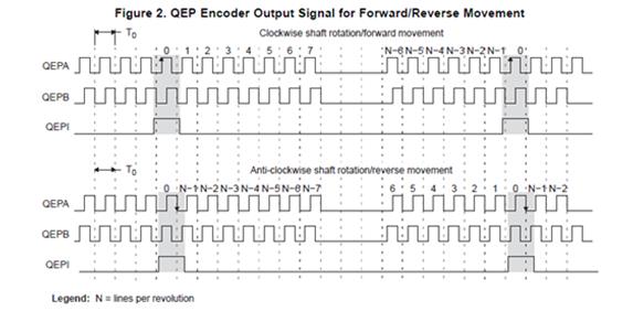
The encoder wheel typically makes one revolution for every revolution of the motor, or the wheel may be at a geared rotation ratio with respect to the motor. Therefore, the frequency of the digital signal coming from the QEPA and QEPB outputs varies proportionally with the velocity of the motor. For example, a 2000-line encoder directly coupled to a motor running at 5000 revolutions per minute (rpm) results in a frequency of 166.6 KHz, so by measuring the frequency of either the QEPA or QEPB output, the processor can determine the velocity of the motor.
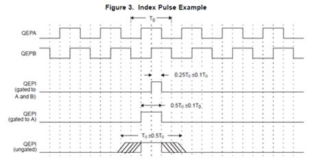
Quadrature encoders from different manufacturers come with two forms of index pulse (gated index pulse or un-gated index pulse) as shown in Figure 3. A nonstandard form of index pulse is un-gated. In the un-gated configuration, the index edges are not necessarily coincident with A and B signals. The gated index pulse is aligned to any of the four quadrature edges and width of the index pulse and can be equal to a quarter, half, or full period of the quadrature signal.
Some typical applications of shaft encoders include robotics and even computer input in the form of a mouse. Inside your mouse you can see where the mouse ball spins a pair of axles (a left/right, and an up/down axle). These axles are connected to optical shaft encoders that effectively tell the computer how fast and in what direction the mouse is moving.
General Issues:
Estimating velocity from a digital position sensor is a cost-effective strategy in motor control. Two different first order approximations for velocity may be written as:
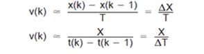
Where:
v(k): Velocity at time instant k
x(k): Position at time instant k
x(k-1): Position at time instant k-1
T: Fixed unit time or inverse of velocity calculation rate
∆X: Incremental position movement in unit time
t(k): Time instant “k”
t(k-1): Time instant “k-1”
X: Fixed unit position
∆T: Incremental time elapsed for unit position movement.
Equation 1 is the conventional approach to velocity estimation, and it requires a time base to provide unit time event for velocity calculation. Unit time is basically the inverse of the velocity calculation rate.
The encoder count (position) is read once during each unit time event. The quantity [x(k) - x(k-1)] is formed by subtracting the previous reading from the current reading. Then the velocity estimate is computed by multiplying by the known constant 1/T (where T is the constant time between unit time events and is known in advance).
Estimation based on Equation 1 has an inherent accuracy limit directly related to the resolution of the position sensor and the unit time T. For example, consider a 500-line per revolution quadrature encoder with a velocity calculation rate of 400 Hz. When used for positioning the quadrature encoder gives a four-fold increase in resolution, in this case, 2000 counts per revolution. The minimum rotation that can be detected is therefore 0.0005 revolutions, which gives a velocity resolution of 12 rpm when sampled at 400 Hz. While this resolution may be satisfactory at moderate or high speeds, e.g. 1% error at 1200 rpm, it would clearly prove inadequate at low speeds. In fact, at speeds below 12 rpm, the speed estimate would erroneously be zero much of the time.
At low speed, Equation 2 provides a more accurate approach. It requires a position sensor that outputs a fixed interval pulse train, such as the quadrature encoder. The width of each pulse is defined by motor speed for a given sensor resolution. Equation 2 can be used to calculate motor speed by measuring the elapsed time between successive quadrature pulse edges. However, this method suffers from the opposite limitation, as does Equation 1. A combination of relatively large motor speeds and high sensor resolution makes the time interval ∆T small, and thus more greatly influenced by the timer resolution. This can introduce considerable error into high-speed estimates.
For systems with a large speed range (that is, speed estimation is needed at both low and high speeds), one approach is to use Equation 2 at low speed and have the DSP software switch over to Equation 1 when the motor speed rises above some specified threshold.
APPENDIX B: PIN-OUT DETAILS
Pin-out details (for reference) are shown below, with respect to DATAIO. Additional information on pin-outs can be found in the Motherboard Operational Manuals.
| Module Signal(Ref Only) | 44-Pin I/O | 50-Pin I/O (Mod Slot 1-J3) | 50-Pin I/O (Mod Slot 2-J4) | 50-Pin I/O (Mod Slot 3-J3) | 50-Pin I/O (Mod Slot 3-J4) | Encoder, 4 CH (EC1) |
| DATIO1 | 2 | 10 | 1 | 2 | AP-CH1 | |
| DATIO2 | 24 | 35 | 26 | 27 | AN-CH1 | |
| DATIO3 | 3 | 11 | 2 | 3 | BP-CH1 | |
| DATIO4 | 25 | 36 | 27 | 28 | BN-CH1 | |
| DATIO5 | 5 | 13 | 4 | 5 | N/C (undefined) | |
| DATIO6 | 27 | 38 | 29 | 30 | ISO_A | |
| DATIO7 | 7 | 14 | 5 | 6 | AP-CH2 | |
| DATIO8 | 29 | 39 | 30 | 31 | AN-CH2 | |
| DATIO9 | 8 | 15 | 6 | 7 | BP-CH2 | |
| DATIO10 | 30 | 40 | 31 | 32 | BN-CH2 | |
| DATIO11 | 10 | 17 | 8 | 9 | N/C (undefined) | |
| DATIO12 | 32 | 42 | 33 | 34 | ISO_B | |
| DATIO13 | 12 | 18 | 9 | 17 | AP-CH3 | |
| DATIO14 | 34 | 43 | 34 | 42 | AN-CH3 | |
| DATIO15 | 13 | 19 | 10 | 18 | BP-CH3 | |
| DATIO16 | 35 | 44 | 35 | 43 | BN-CH3 | |
| DATIO17 | 15 | 21 | 12 | 20 | N/C (undefined) | |
| DATIO18 | 37 | 46 | 37 | 45 | ISO_C | |
| DATIO19 | 17 | 22 | 13 | 21 | AP-CH4 | |
| DATIO20 | 39 | 47 | 38 | 46 | AN-CH4 | |
| DATIO21 | 18 | 23 | 14 | 22 | BP-CH4 | |
| DATIO22 | 40 | 48 | 39 | 47 | BN-CH4 | |
| DATIO23 | 20 | 25 | 16 | 24 | N/C (undefined) | |
| DATIO24 | 42 | 50 | 41 | 49 | ISO_D | |
| DATIO25 | 4 | 12 | 3 | 4 | CP-CH1 | |
| DATIO26 | 26 | 37 | 28 | 29 | CN-CH1 | |
| DATIO27 | 9 | 16 | 7 | 8 | CP-CH2 | |
| DATIO28 | 31 | 41 | 32 | 33 | CN-CH2 | |
| DATIO29 | 14 | 20 | 11 | 19 | CP-CH3 | |
| DATIO30 | 36 | 45 | 36 | 44 | CN-CH3 | |
| DATIO31 | 19 | 24 | 15 | 23 | CP-CH4 | |
| DATIO32 | 41 | 49 | 40 | 48 | CN-CH4 | |
| DATIO33 | 6 | N/C | ||||
| DATIO34 | 28 | N/C | ||||
| DATIO35 | 11 | N/C | ||||
| DATIO36 | 33 | N/C | ||||
| DATIO37 | 16 | N/C | ||||
| DATIO38 | 38 | N/C | ||||
| DATIO39 | 21 | N/C | ||||
| DATIO40 | 43 | N/C | ||||
| N/A |
REVISION HISTORY
| Revision Date | Description |
|---|---|
| 2026-01-20 | Initial release to docs.naii |
STATUS AND INTERRUPTS
Status registers indicate the detection of faults or events. The status registers can be channel bit-mapped or event bit-mapped. An example of a channel bit-mapped register is the BIT status register, and an example of an event bit-mapped register is the FIFO status register.
For those status registers that allow interrupts to be generated upon the detection of the fault or the event, there are four registers associated with each status: Dynamic, Latched, Interrupt Enabled, and Set Edge/Level Interrupt.
Dynamic Status: The Dynamic Status register indicates the current condition of the fault or the event. If the fault or the event is momentary, the contents in this register will be clear when the fault or the event goes away. The Dynamic Status register can be polled, however, if the fault or the event is sporadic, it is possible for the indication of the fault or the event to be missed.
Latched Status: The Latched Status register indicates whether the fault or the event has occurred and keeps the state until it is cleared by the user. Reading the Latched Status register is a better alternative to polling the Dynamic Status register because the contents of this register will not clear until the user commands to clear the specific bit(s) associated with the fault or the event in the Latched Status register. Once the status register has been read, the act of writing a 1 back to the applicable status register to any specific bit (channel/event) location will “clear” the bit (set the bit to 0). When clearing the channel/event bits, it is strongly recommended to write back the same bit pattern as read from the Latched Status register. For example, if the channel bit-mapped Latched Status register contains the value 0x0000 0005, which indicates fault/event detection on channel 1 and 3, write the value 0x0000 0005 to the Latched Status register to clear the fault/event status for channel 1 and 3. Writing a “1” to other channels that are not set (example 0x0000 000F) may result in incorrectly “clearing” incoming faults/events for those channels (example, channel 2 and 4).
Interrupt Enable: If interrupts are preferred upon the detection of a fault or an event, enable the specific channel/event interrupt in the Interrupt Enable register. The bits in Interrupt Enable register map to the same bits in the Latched Status register. When a fault or event occurs, an interrupt will be fired. Subsequent interrupts will not trigger until the application acknowledges the fired interrupt by clearing the associated channel/event bit in the Latched Status register. If the interruptible condition is still persistent after clearing the bit, this may retrigger the interrupt depending on the Edge/Level setting.
Set Edge/Level Interrupt: When interrupts are enabled, the condition on retriggering the interrupt after the Latch Register is “cleared” can be specified as “edge” triggered or “level” triggered. Note, the Edge/Level Trigger also affects how the Latched Register value is adjusted after it is “cleared” (see below).
Edge triggered: An interrupt will be retriggered when the Latched Status register change from low (0) to high (1) state. Uses for edge-triggered interrupts would include transition detections (Low-to-High transitions, High-to-Low transitions) or fault detections. After “clearing” an interrupt, another interrupt will not occur until the next transition or the re-occurrence of the fault again.
Level triggered: An interrupt will be generated when the Latched Status register remains at the high (1) state. Level-triggered interrupts are used to indicate that something needs attention.
Interrupt Vector and Steering
When interrupts are enabled, the interrupt vector associated with the specific interrupt can be programmed with a unique number/identifier defined by the user such that it can be utilized in the Interrupt Service Routine (ISR) to identify the type of interrupt. When an interrupt occurs, the contents of the Interrupt Vector registers is reported as part of the interrupt mechanism. In addition to specifying the interrupt vector, the interrupt can be directed (“steered”) to the native bus or to the application running on the onboard ARM processor.
Interrupt Trigger Types
In most applications, limiting the number of interrupts generated is preferred as interrupts are costly, thus choosing the correct Edge/Level interrupt trigger to use is important.
Example 1: Fault detection
This example illustrates interrupt considerations when detecting a fault like an “open” on a line. When an “open” is detected, the system will receive an interrupt. If the “open” on the line is persistent and the trigger is set to “edge”, upon “clearing” the interrupt, the system will not regenerate another interrupt. If, instead, the trigger is set to “level”, upon “clearing” the interrupt, the system will re-generate another interrupt. Thus, in this case, it will be better to set the trigger type to “edge”.
Example 2: Threshold detection
This example illustrates interrupt considerations when detecting an event like reaching or exceeding the “high watermark” threshold value. In a communication device, when the number of elements received in the FIFO reaches the high-watermark threshold, an interrupt will be generated. Normally, the application would read the count of the number of elements in the FIFO and read this number of elements from the FIFO. After reading the FIFO data, the application would “clear” the interrupt. If the trigger type is set to “edge”, another interrupt will be generated only if the number of elements in FIFO goes below the “high watermark” after the “clearing” the interrupt and then fills up to reach the “high watermark” threshold value. Since receiving communication data is inherently asynchronous, it is possible that data can continue to fill the FIFO as the application is pulling data off the FIFO. If, at the time the interrupt is “cleared”, the number of elements in the FIFO is at or above the “high watermark”, no interrupts will be generated. In this case, it will be better to set the trigger type to “level”, as the purpose here is to make sure that the FIFO is serviced when the number of elements exceeds the high watermark threshold value. Thus, upon “clearing” the interrupt, if the number of elements in the FIFO is at or above the “high watermark” threshold value, another interrupt will be generated indicating that the FIFO needs to be serviced.
Dynamic and Latched Status Registers Examples
The examples in this section illustrate the differences in behavior of the Dynamic Status and Latched Status registers as well as the differences in behavior of Edge/Level Trigger when the Latched Status register is cleared.
Figure 1. Example of Module's Channel-Mapped Dynamic and Latched Status States
No Clearing of
Latched StatusClearing of Latched Status
(Edge-Triggered)Clearing of Latched Status
(Level-Triggered)Time Dynamic Status Latched Status Action Latched Status Action Latched T0 0x0 0x0 Read Latched Register 0x0 Read Latched Register 0x0 T1 0x1 0x1 Read Latched Register 0x1 0x1 T1 0x1 0x1 Write 0x1 to Latched Register Write 0x1 to Latched Register T1 0x1 0x1 0x0 0x1 T2 0x0 0x1 Read Latched Register 0x0 Read Latched Register 0x1 T2 0x0 0x1 Read Latched Register 0x0 Write 0x1 to Latched Register T2 0x0 0x1 Read Latched Register 0x0 0x0 T3 0x2 0x3 Read Latched Register 0x2 Read Latched Register 0x2 T3 0x2 0x3 Write 0x2 to Latched Register Write 0x2 to Latched Register T3 0x2 0x3 0x0 0x2 T4 0x2 0x3 Read Latched Register 0x1 Read Latched Register 0x3 T4 0x2 0x3 Write 0x1 to Latched Register Write 0x3 to Latched Register T4 0x2 0x3 0x0 0x2 T5 0xC 0xF Read Latched Register 0xC Read Latched Register 0xE T5 0xC 0xF Write 0xC to Latched Register Write 0xE to Latched Register T5 0xC 0xF 0x0 0xC T6 0xC 0xF Read Latched Register 0x0 Read Latched 0xC T6 0xC 0xF Read Latched Register 0x0 Write 0xC to Latched Register T6 0xC 0xF Read Latched Register 0x0 0xC T7 0x4 0xF Read Latched Register 0x0 Read Latched Register 0xC T7 0x4 0xF Read Latched Register 0x0 Write 0xC to Latched Register T7 0x4 0xF Read Latched Register 0x0 0x4 T8 0x4 0xF Read Latched Register 0x0 Read Latched Register 0x4 Interrupt Examples
The examples in this section illustrate the interrupt behavior with Edge/Level Trigger.
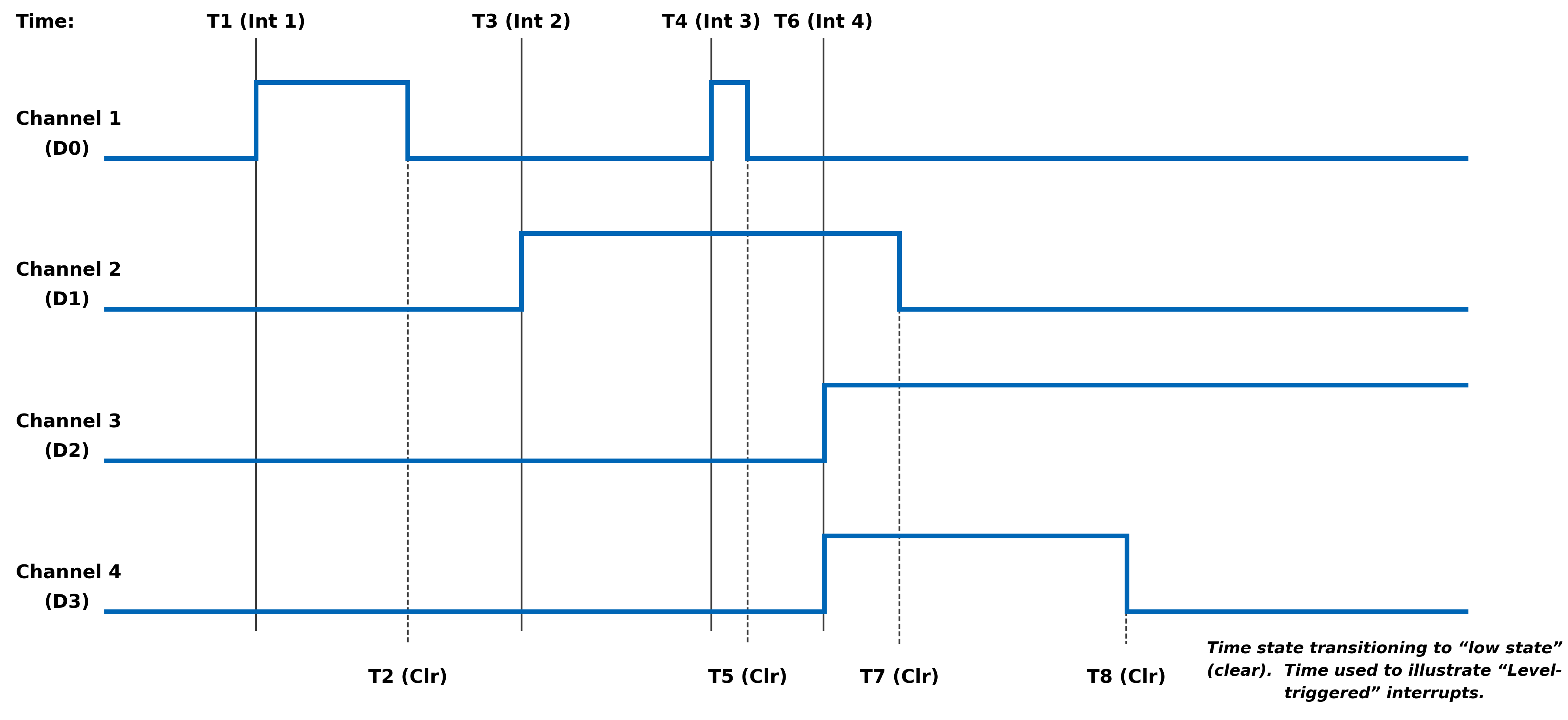
Figure 2. Illustration of Latched Status State for Module with 4-Channels with Interrupt Enabled
Time Latched Status
(Edge-Triggered -
Clear Multi-Channel)Latched Status
(Edge-Triggered -
Clear Single Channel)Latched Status
(Level-Triggered -
Clear Multi-Channel)Action Latched Action Latched Action Latched T1
(Int 1)Interrupt Generated
Read Latched Registers0x1 Interrupt Generated
Read Latched Registers0x1 Interrupt Generated
Read Latched Registers0x1 T1
(Int 1)Write 0x1 to Latched Register Write 0x1 to Latched Register Write 0x1 to Latched Register T1
(Int 1)0x0 0x0 Interrupt re-triggers
Note, interrupt re-triggers after
each clear until T2.0x1 T3
(Int 2)Interrupt Generated
Read Latched Registers0x2 Interrupt Generated
Read Latched Registers0x2 Interrupt Generated
Read Latched Registers0x2 T3
(Int 2)Write 0x2 to Latched Register Write 0x2 to Latched Register Write 0x2 to Latched Register T3
(Int 2)0x0 0x0 Interrupt re-triggers
Note, interrupt re-triggers after
each clear until T7.0x2 T4
(Int 3)Interrupt Generated
Read Latched Registers0x1 Interrupt Generated
Read Latched Registers0x1 Interrupt Generated
Read Latched Registers0x3 T4
(Int 3)Write 0x1 to Latched Register Write 0x1 to Latched Register Write 0x3 to Latched Register T4
(Int 3)0x0 0x0 Interrupt re-triggers
Note, interrupt re-triggers after
each clear and 0x3 is reported
in Latched Register until T5.0x3 T4
(Int 3)0x0 0x0 Interrupt re-triggers
Note, interrupt re-triggers after
each clear until T7.0x2 T6
(Int 4)Interrupt Generated
Read Latched Registers0xC Interrupt Generated
Read Latched Registers0xC Interrupt Generated
Read Latched Registers0xE T6
(Int 4)Write 0xC to Latched Register Write 0x4 to Latched Register Write 0xE to Latched Register T6
(Int 4)0x0 Interrupt re-triggers
Write 0x8 to Latched Register0x8 Interrupt re-triggers
Note, interrupt re-triggers after
each clear and 0xE is
reported in Latched Register until T7.0xE T6
(Int 4)0x0 0x0 Interrupt re-triggers
Note, interrupt re-triggers after
each clear and 0xC is
reported in Latched Register until T8.0xC T6
(Int 4)0x0 0x0 Interrupt re-triggers
Note, interrupt re-triggers after
each clear and 0x4 is
reported in Latched Register always.0x4 REVISION HISTORY
Motherboard Manual - Status and Interrupts Revision History Revision Revision Date Description C 2021-11-30 C08896; Transition manual to docbuilder format - no technical info change. Link to original
DOCS.NAII REVISIONS Revision Date Description 2026-03-02 Formatting updates to document; no technical changes. 2026-05-18 Fixed formatting issues from conversion to new doc site format. 2026-05-19 Fixed minor formatting issue with Interrupt Examples table structure (removed extraneous cell). 2026-07-15 Revised image files for image quality.
MODULE COMMON REGISTERS
The registers described in this document are common to all NAI Generation 5 modules.
Module Information Registers
The registers in this section provide module information such as firmware revisions, capabilities and unique serial number information.
FPGA Version Registers
The FPGA firmware version registers include registers that contain the Revision, Compile Timestamp, SerDes Revision, Template Revision and Zynq Block Revision information.
FPGA Revision Function: FPGA firmware revision Type: unsigned binary word (32-bit) Data Range: 0x0000 0000 to 0xFFFF FFFF Read/Write: R Initialized Value: Value corresponding to the revision of the board's FPGA Operational Settings: The upper 16-bits are the major revision and the lower 16-bits are the minor revision.
D31 D30 D29 D28 D27 D26 D25 D24 D23 D22 D21 D20 D19 D18 D17 D16 Major Revision Number D15 D14 D13 D12 D11 D10 D9 D8 D7 D6 D5 D4 D3 D2 D1 D0 Minor Revision Number
FPGA Compile Timestamp Function: Compile Timestamp for the FPGA firmware. Type: unsigned binary word (32-bit) Data Range: N/A Read/Write: R Initialized Value: Value corresponding to the compile timestamp of the board's FPGA Operational Settings: The 32-bit value represents the Day, Month, Year, Hour, Minutes and Seconds as formatted in the table:
D31 D30 D29 D28 D27 D26 D25 D24 D23 D22 D21 D20 D19 D18 D17 D16 day (5-bits) month (4-bits) year (6-bits) hr D15 D14 D13 D12 D11 D10 D9 D8 D7 D6 D5 D4 D3 D2 D1 D0 hour (5-bits) minutes (6-bits) seconds (6-bits)
FPGA SerDes Revision Function: FPGA SerDes revision Type: unsigned binary word (32-bit) Data Range: 0x0000 0000 to 0xFFFF FFFF Read/Write: R Initialized Value: Value corresponding to the SerDes revision of the board's FPGA Operational Settings: The upper 16-bits are the major revision, and the lower 16-bits are the minor revision.
D31 D30 D29 D28 D27 D26 D25 D24 D23 D22 D21 D20 D19 D18 D17 D16 Major Revision Number D15 D14 D13 D12 D11 D10 D9 D8 D7 D6 D5 D4 D3 D2 D1 D0 Minor Revision Number
FPGA Template Revision Function: FPGA Template revision Type: unsigned binary word (32-bit) Data Range: 0x0000 0000 to 0xFFFF FFFF Read/Write: R Initialized Value: Value corresponding to the template revision of the board's FPGA Operational Settings: The upper 16-bits are the major revision, and the lower 16-bits are the minor revision.
D31 D30 D29 D28 D27 D26 D25 D24 D23 D22 D21 D20 D19 D18 D17 D16 Major Revision Number D15 D14 D13 D12 D11 D10 D9 D8 D7 D6 D5 D4 D3 D2 D1 D0 Minor Revision Number
FPGA Zynq Block Revision Function: FPGA Zynq Block revision Type: unsigned binary word (32-bit) Data Range: 0x0000 0000 to 0xFFFF FFFF Read/Write: R Initialized Value: Value corresponding to the Zynq block revision of the board's FPGA Operational Settings: The upper 16-bits are the major revision, and the lower 16-bits are the minor revision.
D31 D30 D29 D28 D27 D26 D25 D24 D23 D22 D21 D20 D19 D18 D17 D16 Major Revision Number D15 D14 D13 D12 D11 D10 D9 D8 D7 D6 D5 D4 D3 D2 D1 D0 Minor Revision Number Bare Metal Version Registers
The Bare Metal firmware version registers include registers that contain the Revision and Compile Time information.
Bare Metal Revision Function: Bare Metal firmware revision Type: unsigned binary word (32-bit) Data Range: 0x0000 0000 to 0xFFFF FFFF Read/Write: R Initialized Value: Value corresponding to the revision of the board's Bare Metal Operational Settings: The upper 16-bits are the major revision and the lower 16-bits are the minor revision.
D31 D30 D29 D28 D27 D26 D25 D24 D23 D22 D21 D20 D19 D18 D17 D16 Major Revision Number D15 D14 D13 D12 D11 D10 D9 D8 D7 D6 D5 D4 D3 D2 D1 D0 Minor Revision Number
Bare Metal Compile Time Function: Provides an ASCII representation of the Date/Time for the Bare Metal compile time. Type: 24-character ASCII string - Six (6) unsigned binary word (32-bit) Data Range: N/A Read/Write: R Initialized Value: Value corresponding to the ASCII representation of the compile time of the board's Bare Metal Operational Settings: The six 32-bit words provide an ASCII representation of the Date/Time. The hexadecimal values in the field below represent: May 17 2019 at 15:38:32 Note
little-endian order of ASCII values
Word 1 (Ex. 0x2079614D) D31 D30 D29 D28 D27 D26 D25 D24 D23 D22 D21 D20 D19 D18 D17 D16 Space (0x20) Month ('y' - 0x79) D15 D14 D13 D12 D11 D10 D9 D8 D7 D6 D5 D4 D3 D2 D1 D0 Month ('a' - 0x61) Month ('M' - 0x4D) Word 2 (Ex. 0x32203731) D31 D30 D29 D28 D27 D26 D25 D24 D23 D22 D21 D20 D19 D18 D17 D16 Year ('2' - 0x32) Space (0x20) D15 D14 D13 D12 D11 D10 D9 D8 D7 D6 D5 D4 D3 D2 D1 D0 Day ('7' - 0x37) Day ('1' - 0x31) Word 3 (Ex. 0x20393130) D31 D30 D29 D28 D27 D26 D25 D24 D23 D22 D21 D20 D19 D18 D17 D16 Space (0x20) Year ('9' - 0x39) D15 D14 D13 D12 D11 D10 D9 D8 D7 D6 D5 D4 D3 D2 D1 D0 Year ('1' - 0x31) Year ('0' - 0x30) Word 4 (Ex. 0x31207461) D31 D30 D29 D28 D27 D26 D25 D24 D23 D22 D21 D20 D19 D18 D17 D16 Hour ('1' - 0x31) Space (0x20) D15 D14 D13 D12 D11 D10 D9 D8 D7 D6 D5 D4 D3 D2 D1 D0 'a' (0x74) 't' (0x61) Word 5 (Ex. 0x38333A35) D31 D30 D29 D28 D27 D26 D25 D24 D23 D22 D21 D20 D19 D18 D17 D16 Minute ('8' - 0x38) Minute ('3' - 0x33) D15 D14 D13 D12 D11 D10 D9 D8 D7 D6 D5 D4 D3 D2 D1 D0 ':' (0x3A) Hour ('5' - 0x35) Word 6 (Ex. 0x0032333A) D31 D30 D29 D28 D27 D26 D25 D24 D23 D22 D21 D20 D19 D18 D17 D16 NULL (0x00) Seconds ('2' - 0x32) D15 D14 D13 D12 D11 D10 D9 D8 D7 D6 D5 D4 D3 D2 D1 D0 Seconds ('3' - 0x33) ':' (0x3A) FSBL Version Registers
The FSBL version registers include registers that contain the Revision and Compile Time information for the First Stage Boot Loader (FSBL).
FSBL Revision Function: FSBL firmware revision Type: unsigned binary word (32-bit) Data Range: 0x0000 0000 to 0xFFFF FFFF Read/Write: R Initialized Value: Value corresponding to the revision of the board's FSBL Operational Settings: The upper 16-bits are the major revision, and the lower 16-bits are the minor revision.
D31 D30 D29 D28 D27 D26 D25 D24 D23 D22 D21 D20 D19 D18 D17 D16 Major Revision Number D15 D14 D13 D12 D11 D10 D9 D8 D7 D6 D5 D4 D3 D2 D1 D0 Minor Revision Number
FSBL Compile Time Function: Provides an ASCII representation of the Date/Time for the FSBL compile time. Type: 24-character ASCII string - Six (6) unsigned binary word (32-bit) Data Range: N/A Read/Write: R Initialized Value: Value corresponding to the ASCII representation of the Compile Time of the board's FSBL Operational Settings: The six 32-bit words provide an ASCII representation of the Date/Time. The hexadecimal values in the field below represent: May 17 2019 at 15:38:32
Note
little-endian order of ASCII values
Word 1 (Ex. 0x2079614D) D31 D30 D29 D28 D27 D26 D25 D24 D23 D22 D21 D20 D19 D18 D17 D16 Space (0x20) Month ('y' - 0x79) D15 D14 D13 D12 D11 D10 D9 D8 D7 D6 D5 D4 D3 D2 D1 D0 Month ('a' - 0x61) Month ('M' - 0x4D) Word 2 (Ex. 0x32203731) D31 D30 D29 D28 D27 D26 D25 D24 D23 D22 D21 D20 D19 D18 D17 D16 Year ('2' - 0x32) Space (0x20) D15 D14 D13 D12 D11 D10 D9 D8 D7 D6 D5 D4 D3 D2 D1 D0 Day ('7' - 0x37) Day ('1' - 0x31) Word 3 (Ex. 0x20393130) D31 D30 D29 D28 D27 D26 D25 D24 D23 D22 D21 D20 D19 D18 D17 D16 Space (0x20) Year ('9' - 0x39) D15 D14 D13 D12 D11 D10 D9 D8 D7 D6 D5 D4 D3 D2 D1 D0 Year ('1' - 0x31) Year ('0' - 0x30) Word 4 (Ex. 0x31207461) D31 D30 D29 D28 D27 D26 D25 D24 D23 D22 D21 D20 D19 D18 D17 D16 Hour ('1' - 0x31) Space (0x20) D15 D14 D13 D12 D11 D10 D9 D8 D7 D6 D5 D4 D3 D2 D1 D0 'a' (0x74) 't' (0x61) Word 5 (Ex. 0x38333A35) D31 D30 D29 D28 D27 D26 D25 D24 D23 D22 D21 D20 D19 D18 D17 D16 Minute ('8' - 0x38) Minute ('3' - 0x33) D15 D14 D13 D12 D11 D10 D9 D8 D7 D6 D5 D4 D3 D2 D1 D0 ':' (0x3A) Hour ('5' - 0x35) Word 6 (Ex. 0x0032333A) D31 D30 D29 D28 D27 D26 D25 D24 D23 D22 D21 D20 D19 D18 D17 D16 NULL (0x00) Seconds ('2' - 0x32) D15 D14 D13 D12 D11 D10 D9 D8 D7 D6 D5 D4 D3 D2 D1 D0 Seconds ('3' - 0x33) ':' (0x3A) Module Serial Number Registers
The Module Serial Number registers include registers that contain the Serial Numbers for the Interface Board and the Functional Board of the module.
Interface Board Serial Number Function: Unique 128-bit identifier used to identify the interface board. Type: 16-character ASCII string - Four (4) unsigned binary words (32-bit) Data Range: N/A Read/Write: R Initialized Value: Serial number of the interface board Operational Settings: This register is for information purposes only.
Functional Board Serial Number Function: Unique 128-bit identifier used to identify the functional board. Type: 16-character ASCII string - Four (4) unsigned binary words (32-bit) Data Range: N/A Read/Write: R Initialized Value: Serial number of the functional board Operational Settings: This register is for information purposes only.
Module Capability Function: Provides indication for whether or not the module can support the following: SerDes block reads, SerDes FIFO block reads, SerDes packing (combining two 16-bit values into one 32-bit value) and floating point representation. The purpose for block access and packing is to improve the performance of accessing larger amounts of data over the SerDes interface. Type: unsigned binary word (32-bit) Data Range: 0x0000 0000 to 0x0000 0107 Read/Write: R Initialized Value: 0x0000 0107 Operational Settings: A “1” in the bit associated with the capability indicates that it is supported.
D31 D30 D29 D28 D27 D26 D25 D24 D23 D22 D21 D20 D19 D18 D17 D16 0 0 0 0 0 0 0 0 0 0 0 0 0 0 0 0 D15 D14 D13 D12 D11 D10 D9 D8 D7 D6 D5 D4 D3 D2 D1 D0 0 0 0 0 0 0 0 Flt-Pt 0 0 0 0 0 Pack FIFO Blk Blk
Module Memory Map Revision Function: Module Memory Map revision Type: unsigned binary word (32-bit) Data Range: 0x0000 0000 to 0xFFFF FFFF Read/Write: R Initialized Value: Value corresponding to the Module Memory Map Revision Operational Settings: The upper 16-bits are the major revision and the lower 16-bits are the minor revision.
D31 D30 D29 D28 D27 D26 D25 D24 D23 D22 D21 D20 D19 D18 D17 D16 Major Revision Number D15 D14 D13 D12 D11 D10 D9 D8 D7 D6 D5 D4 D3 D2 D1 D0 Minor Revision Number Module Measurement Registers
The registers in this section provide module temperature measurement information.
Temperature Readings Registers
The temperature registers provide the current, maximum (from power-up) and minimum (from power-up) Zynq and PCB temperatures.
Interface Board Current Temperature Function: Measured PCB and Zynq Core temperatures on Interface Board. Type: signed byte (8-bits) for PCB and signed byte (8-bits) for Zynq core temperatures Data Range: 0x0000 0000 to 0x0000 FFFF Read/Write: R Initialized Value: Value corresponding to the measured PCB and Zynq core temperatures based on the table below Operational Settings: The upper 16-bits are not used, and the lower 16-bits are the PCB and Zynq Core Temperatures. For example, if the register contains the value 0x0000 202C, this represents PCB Temperature = 32° Celsius and Zynq Temperature = 44° Celsius.
D31 D30 D29 D28 D27 D26 D25 D24 D23 D22 D21 D20 D19 D18 D17 D16 0 0 0 0 0 0 0 0 0 0 0 0 0 0 0 0 D15 D14 D13 D12 D11 D10 D9 D8 D7 D6 D5 D4 D3 D2 D1 D0 PCB Temperature Zynq Core Temperature
Functional Board Current Temperature Function: Measured PCB temperature on Functional Board. Type: signed byte (8-bits) for PCB Data Range: 0x0000 0000 to 0x0000 00FF Read/Write: R Initialized Value: Value corresponding to the measured PCB on the table below Operational Settings: The upper 24-bits are not used, and the lower 8-bits are the PCB Temperature. For example, if the register contains the value 0x0000 0019, this represents PCB Temperature = 25° Celsius.
D31 D30 D29 D28 D27 D26 D25 D24 D23 D22 D21 D20 D19 D18 D17 D16 0 0 0 0 0 0 0 0 0 0 0 0 0 0 0 0 D15 D14 D13 D12 D11 D10 D9 D8 D7 D6 D5 D4 D3 D2 D1 D0 0 0 0 0 0 0 0 0 PCB Temperature
Interface Board Maximum Temperature Function: Maximum PCB and Zynq Core temperatures on Interface Board since power-on. Type: signed byte (8-bits) for PCB and signed byte (8-bits) for Zynq core temperatures Data Range: 0x0000 0000 to 0x0000 FFFF Read/Write: R Initialized Value: Value corresponding to the maximum measured PCB and Zynq core temperatures since power-on based on the table below Operational Settings: The upper 16-bits are not used, and the lower 16-bits are the maximum PCB and Zynq Core Temperatures. For example, if the register contains the value 0x0000 5569, this represents maximum PCB Temperature = 85° Celsius and maximum Zynq Temperature = 105° Celsius.
D31 D30 D29 D28 D27 D26 D25 D24 D23 D22 D21 D20 D19 D18 D17 D16 0 0 0 0 0 0 0 0 0 0 0 0 0 0 0 0 D15 D14 D13 D12 D11 D10 D9 D8 D7 D6 D5 D4 D3 D2 D1 D0 PCB Temperature Zynq Core Temperature
Interface Board Minimum Temperature Function: Minimum PCB and Zynq Core temperatures on Interface Board since power-on. Type: signed byte (8-bits) for PCB and signed byte (8-bits) for Zynq core temperatures Data Range: 0x0000 0000 to 0x0000 FFFF Read/Write: R Initialized Value: Value corresponding to the minimum measured PCB and Zynq core temperatures since power-on based on the table below Operational Settings: The upper 16-bits are not used, and the lower 16-bits are the minimum PCB and Zynq Core Temperatures. For example, if the register contains the value 0x0000 D8E7, this represents minimum PCB Temperature = -40° Celsius and minimum Zynq Temperature = -25° Celsius.
D31 D30 D29 D28 D27 D26 D25 D24 D23 D22 D21 D20 D19 D18 D17 D16 0 0 0 0 0 0 0 0 0 0 0 0 0 0 0 0 D15 D14 D13 D12 D11 D10 D9 D8 D7 D6 D5 D4 D3 D2 D1 D0 PCB Temperature Zynq Core Temperature
Functional Board Maximum Temperature Function: Maximum PCB temperature on Functional Board since power-on. Type: signed byte (8-bits) for PCB Data Range: 0x0000 0000 to 0x0000 00FF Read/Write: R Initialized Value: Value corresponding to the measured PCB on the table below Operational Settings: The upper 24-bits are not used, and the lower 8-bits are the PCB Temperature. For example, if the register contains the value 0x0000 0055, this represents PCB Temperature = 85° Celsius.
D31 D30 D29 D28 D27 D26 D25 D24 D23 D22 D21 D20 D19 D18 D17 D16 0 0 0 0 0 0 0 0 0 0 0 0 0 0 0 0 D15 D14 D13 D12 D11 D10 D9 D8 D7 D6 D5 D4 D3 D2 D1 D0 0 0 0 0 0 0 0 0 PCB Temperature
Functional Board Minimum Temperature Function: Minimum PCB temperature on Functional Board since power-on. Type: signed byte (8-bits) for PCB Data Range: 0x0000 0000 to 0x0000 00FF Read/Write: R Initialized Value: Value corresponding to the measured PCB on the table below Operational Settings: The upper 24-bits are not used, and the lower 8-bits are the PCB Temperature. For example, if the register contains the value 0x0000 00D8, this represents PCB Temperature = -40° Celsius.
D31 D30 D29 D28 D27 D26 D25 D24 D23 D22 D21 D20 D19 D18 D17 D16 0 0 0 0 0 0 0 0 0 0 0 0 0 0 0 0 D15 D14 D13 D12 D11 D10 D9 D8 D7 D6 D5 D4 D3 D2 D1 D0 0 0 0 0 0 0 0 0 PCB Temperature Higher Precision Temperature Readings Registers
These registers provide higher precision readings of the current Zynq and PCB temperatures.
Higher Precision Zynq Core Temperature Function: Higher precision measured Zynq Core temperature on Interface Board. Type: signed word (16-bits) for integer part and unsigned word (16-bits) for fractional part Data Range: 0x0000 0000 to 0xFFFF FFFF Read/Write: R Initialized Value: Measured Zynq Core temperature on Interface Board Operational Settings: The upper 16-bits represent the signed integer part of the temperature and the lower 16-bits represent the fractional part of the temperature with the resolution of 1/1000 of degree Celsius. For example, if the register contains the value 0x002B 0271, this represents Zynq Core Temperature = 43.625° Celsius, and value 0xFFF6 0177 represents -10.375° Celsius.
D31 D30 D29 D28 D27 D26 D25 D24 D23 D22 D21 D20 D19 D18 D17 D16 Signed Integer Part of Temperature D15 D14 D13 D12 D11 D10 D9 D8 D7 D6 D5 D4 D3 D2 D1 D0 Fractional Part of Temperature
Higher Precision Interface PCB Temperature Function: Higher precision measured Interface PCB temperature. Type: signed word (16-bits) for integer part and unsigned word (16-bits) for fractional part Data Range: 0x0000 0000 to 0xFFFF FFFF Read/Write: R Initialized Value: Measured Interface PCB temperature Operational Settings: The upper 16-bits represent the signed integer part of the temperature and the lower 16-bits represent the fractional part of the temperature with the resolution of 1/1000 of degree Celsius. For example, if the register contains the value 0x0020 007D, this represents Interface PCB Temperature = 32.125° Celsius, and value 0xFFE8 036B represents -24.875° Celsius.
D31 D30 D29 D28 D27 D26 D25 D24 D23 D22 D21 D20 D19 D18 D17 D16 Signed Integer Part of Temperature D15 D14 D13 D12 D11 D10 D9 D8 D7 D6 D5 D4 D3 D2 D1 D0 Fractional Part of Temperature
Higher Precision Functional PCB Temperature Function: Higher precision measured Functional PCB temperature. Type: signed word (16-bits) for integer part and unsigned word (16-bits) for fractional part Data Range: 0x0000 0000 to 0xFFFF FFFF Read/Write: R Initialized Value: Measured Functional PCB temperature Operational Settings: The upper 16-bits represent the signed integer part of the temperature and the lower 16-bits represent the fractional part of the temperature with the resolution of 1/100 of degree Celsius. For example, if the register contains the value 0x0018 004B, this represents Functional PCB Temperature = 24.75° Celsius, and value 0xFFD9 0019 represents -39.25° Celsius.
D31 D30 D29 D28 D27 D26 D25 D24 D23 D22 D21 D20 D19 D18 D17 D16 Signed Integer Part of Temperature D15 D14 D13 D12 D11 D10 D9 D8 D7 D6 D5 D4 D3 D2 D1 D0 Fractional Part of Temperature Module Health Monitoring Registers
The registers in this section provide module temperature measurement information. If the temperature measurements reaches the Lower Critical or Upper Critical conditions, the module will automatically reset itself to prevent damage to the hardware.
Module Sensor Summary Status Function: The corresponding sensor bit is set if the sensor has crossed any of its thresholds. Type: unsigned binary word (32-bits) Data Range: See table below Read/Write: R Initialized Value: 0 Operational Settings: This register provides a summary for module sensors. When the corresponding sensor bit is set, the Sensor Threshold Status register for that sensor will indicate the threshold condition that triggered the event.
Bit(s) Sensor D31:D6 Reserved D5 Functional Board PCB Temperature D4 Interface Board PCB Temperature D3:D0 Reserved Module Sensor Registers
The registers listed in this section apply to each module sensor listed for the Module Sensor Summary Status register. Each individual sensor register provides a group of registers for monitoring module temperatures readings. From these registers, a user can read the current temperature of the sensor in addition to the minimum and maximum temperature readings since power-up. Upper and lower critical/warning temperature thresholds can be set and monitored from these registers. When a programmed temperature threshold is crossed, the Sensor Threshold Status register will set the corresponding bit for that threshold. The figure below shows the functionality of this group of registers when accessing the Interface Board PCB Temperature sensor as an example.
Sensor Threshold Status Function: Reflects which threshold has been crossed Type: unsigned binary word (32-bits) Data Range: See table below Read/Write: R Initialized Value: 0 Operational Settings: The associated bit is set when the sensor reading exceed the corresponding threshold settings.
Bit(s) Description D31:D4 Reserved D3 Exceeded Upper Critical Threshold D2 Exceeded Upper Warning Threshold D1 Exceeded Lower Critical Threshold D0 Exceeded Lower Warning Threshold
Sensor Current Reading Function: Reflects current reading of temperature sensor Type: Single Precision Floating Point Value (IEEE-754) Data Range: Single Precision Floating Point Value (IEEE-754) Read/Write: R Initialized Value: N/A Operational Settings: The register represents current sensor reading as a single precision floating point value. For example, for a temperature sensor, register value 0x41C6 0000 represents temperature = 24.75° Celsius.
Sensor Minimum Reading Function: Reflects minimum value of temperature sensor since power up Type: Single Precision Floating Point Value (IEEE-754) Data Range: Single Precision Floating Point Value (IEEE-754) Read/Write: R Initialized Value: N/A Operational Settings: The register represents minimum sensor value as a single precision floating point value. For example, for a temperature sensor, register value 0x41C6 0000 represents temperature = 24.75° Celsius.
Sensor Maximum Reading Function: Reflects maximum value of temperature sensor since power up Type: Single Precision Floating Point Value (IEEE-754) Data Range: Single Precision Floating Point Value (IEEE-754) Read/Write: R Initialized Value: N/A Operational Settings: The register represents maximum sensor value as a single precision floating point value. For example, for a temperature sensor, register value 0x41C6 0000 represents temperature = 24.75° Celsius.
Sensor Lower Warning Threshold Function: Reflects lower warning threshold of temperature sensor Type: Single Precision Floating Point Value (IEEE-754) Data Range: Single Precision Floating Point Value (IEEE-754) Read/Write: R/W Initialized Value: Default lower warning threshold (value dependent on specific sensor) Operational Settings: The register represents sensor lower warning threshold as a single precision floating point value. For example, for a temperature sensor, register value 0xC220 0000 represents temperature = -40.0° Celsius.
Sensor Lower Critical Threshold Function: Reflects lower critical threshold of temperature sensor Type: Single Precision Floating Point Value (IEEE-754) Data Range: Single Precision Floating Point Value (IEEE-754) Read/Write: R/W Initialized Value: Default lower critical threshold (value dependent on specific sensor) Operational Settings: The register represents sensor lower critical threshold as a single precision floating point value. For example, for a temperature sensor, register value 0xC25C 0000 represents temperature = -55.0° Celsius.
Sensor Upper Warning Threshold Function: Reflects upper warning threshold of temperature sensor Type: Single Precision Floating Point Value (IEEE-754) Data Range: Single Precision Floating Point Value (IEEE-754) Read/Write: R/W Initialized Value: Default upper warning threshold (value dependent on specific sensor) Operational Settings: The register represents sensor upper warning threshold as a single precision floating point value. For example, for a temperature sensor, register value 0x42AA 0000 represents temperature = 85.0° Celsius.
Sensor Upper Critical Threshold Function: Reflects upper critical threshold of temperature sensor Type: Single Precision Floating Point Value (IEEE-754) Data Range: Single Precision Floating Point Value (IEEE-754) Read/Write: R/W Initialized Value: Default upper critical threshold (value dependent on specific sensor) Operational Settings: The register represents sensor upper critical threshold as a single precision floating point value. For example, for a temperature sensor, register value 0x42FA 0000 represents temperature = 125.0° Celsius. FUNCTION REGISTER MAP
KEY
Configuration/Control Measurement/Status/Board Information
MODULE INFORMATION REGISTERS OFFSET REGISTER NAME ACCESS OFFSET REGISTER NAME ACCESS 0x003C FPGA Revision R 0x0074 Bare Metal Revision R 0x0030 FPGA Compile Timestamp R 0x0080 Bare Metal Compile Time (Bit 0-31) R 0x0034 FPGA SerDes Revision R 0x0084 Bare Metal Compile Time (Bit 32-63) R 0x0038 FPGA Template Revision R 0x0088 Bare Metal Compile Time (Bit 64-95) R 0x0040 FPGA Zynq Block Revision R 0x008C Bare Metal Compile Time (Bit 96-127) R 0x0090 Bare Metal Compile Time (Bit 128-159) R 0x0094 Bare Metal Compile Time (Bit 160-191) R 0x007C FSBL Revision R 0x00B0 FSBL Compile Time (Bit 0-31) R 0x00B4 FSBL Compile Time (Bit 32-63) R 0x00B8 FSBL Compile Time (Bit 64-95) R 0x00BC FSBL Compile Time (Bit 96-127) R 0x00C0 FSBL Compile Time (Bit 128-159) R 0x00C4 FSBL Compile Time (Bit 160-191) R 0x0000 Interface Board Serial Number (Bit 0-31) R 0x0010 Functional Board Serial Number (Bit 0-31) R 0x0034 Interface Board Serial Number (Bit 32-63) R 0x0014 Functional Board Serial Number (Bit 32-63) R 0x0008 Interface Board Serial Number (Bit 64-95) R 0x0018 Functional Board Serial Number (Bit 64-95) R 0x000C Interface Board Serial Number (Bit 96-127) R 0x001C Functional Board Serial Number (Bit 96-127) R 0x0070 Module Capability R 0x01FC Module Memory Map Revision R
MODULE MEASUREMENTS REGISTERS OFFSET REGISTER NAME ACCESS OFFSET REGISTER NAME ACCESS 0x0200 Interface Board PCB/Zynq Current Temp R 0x0208 Functional Board PCB Current Temp R 0x0218 Interface Board PCB/Zynq Max Temp R 0x0228 Functional Board PCB Max Temp R 0x0220 Interface Board PCB/Zynq Min Temp R 0x0230 Functional Board PCB Min Temp R 0x02C0 Higher Precision Zynq Core Temperature R 0x02C4 Higher Precision Interface PCB Temperature R 0x02E0 Higher Precision Functional PCB Temperature R
MODULE HEALTH MONITORING REGISTERS OFFSET REGISTER NAME ACCESS OFFSET REGISTER NAME ACCESS 0x07F8 Module Sensor Summary Status R
REVISION HISTORY
Motherboard Manual - Module Common Registers Revision History Revision Revision Date Description C 2023-08-11 ECO C10649, initial release of module common registers manual. C1 2024-05-15 ECO C11522, removed Zynq Core/Aux/DDR Voltage register descriptions from Module Measurement Registers. Pg.16, updated Module Sensor Summary Status register to add PS references; updated Bit Table to change voltage/current bits to 'reserved'. Pg.16, updated Module/Power Supply Sensor Registers description to better describe register functionality and to add figure. Pg.17, added 'Exceeded' to threshold bit descriptions. Pg.17-18, removed voltage/current references from sensor descriptions. Pg.20, removed Zynq Core/Aux/DDR Voltage register offsets from Module Measurement Registers. Pg.20, updated Module Health Monitoring Registers offset tables. C2 2024-07-10 ECO C11701, pg.16, updated Module Sensor Summary Status register to remove PS references;updated Bit Table to change PS temperature bits to 'reserved'. Pg.16, updated Module SensorRegisters description to remove PS references. Pg.20, updated Module Health MonitoringRegisters offset tables to remove PS temperature register offsets. Link to original
DOCS.NAII REVISIONS Revision Date Description 2025-11-05 Corrected register offsets for Interface Board Min Temp and Function Board Min & Max Temps. 2026-03-02 Formatting updates to document; no technical changes. 2026-05-20 Minor formatting fixes (non-technical changes). 2026-07-15 Updated images for online quality; minor additional formatting updates (no technical changes).


NAI Cares
North Atlantic Industries (NAI) is a leading independent supplier of Embedded I/O Boards, Single Board Computers, Rugged Power Supplies, Embedded Systems and Motion Simulation and Measurement Instruments for the Military, Aerospace and Industrial Industries. We accelerate our clients’ time-to-mission with a unique approach based on a Configurable Open Systems Architecture™ (COSA®) that delivers the best of both worlds: custom solutions from standard COTS components.
We have built a reputation by listening to our customers, understanding their needs, and designing, testing and delivering board and system-level products for their most demanding air, land and sea requirements. If you have any applications or questions regarding the use of our products, please contact us for an expedient solution.
Please visit us at: www.naii.com or select one of the following for immediate assistance:
Documentation
FAQ
Application Notes
http://www.naii.com/applicationnotes
Calibration and Repairs
http://www.naii.com/calibrationrepairs
Call Us
(631) 567-1100
Link to original