DATA SHEET
Click here for the CB1-3 data sheet
INTRODUCTION
As a leading manufacturer of smart function modules, NAI offers over 100 different modules that cover a wide range of I/O, measurements and simulation, communications, Ethernet switch, and SBC functions. Our CANBus smart function modules provide independent, isolated, channels of CAN serial data bus links, conforming to the ISO 11898 International Standard.
CAN (Controller Area Network) is a multi-master, broadcast, serial bus standard for connecting Electronic Control Units (ECUs) in the automotive, aerospace, marine, industrial automation and medical equipment industries. ISO 11898 defines the CAN serial bus system and specifies its architecture and operating parameters. Module CB1 conforms to CAN Specification 2.0, parts A and B. Module CB2 conforms to the SAE J1939 protocol specification, with address claiming option. Module CB3 allows for the selection of either protocol for each channel. The CAN protocol was developed by Robert Bosch GmbH and is recognized and protected by patents and licensed by Bosch.
This user manual is designed to help you get the most out of our CANBus smart function modules.
Note
Firmware Version 1.13 was implemented on 6/20/2017 along with NAIbrd Version 1.44. This update added Source Address (1939), Protocol Assignment and TX/RX Enable State registers. In addition, changes were made to the Communication Status and Control registers.
CB1-CB3 Overview
NAI’s CB1-CB3 modules offers a range of features designed to suit a variety of system requirements, including:
Galvanically Isolated Channels: These modules boast eight independent channels, each equipped with galvanic isolation, ensuring reliable and secure data transmission. The core technology utilizes Bosch® FPGA cores for robust performance.
ANSI-C Compliance: NAI’s CANBus modules adhere to ANSI-C standards for Network, Transport, and DataLink layers, ensuring seamless interoperability with industry standard protocols.
Flexible Addressing Options: Choose from Self-Configurable, Non-Configurable, or Command Configurable addressing options, allowing you to tailor the modules to your specific application requirements.
Protocol Support: CB1 modules support CAN 2.0 A & B protocols, with each channel independently configurable. Meanwhile, CB2 modules are tailored for J1939 protocol, complying with SAE section J1939/21 for Transport and DataLink layers and SAE section J1939/81 for the Network layer. CB3 modules provide the flexibility to support both protocols, enabling channel configuration based on the user’s needs.
Adjustable Baud Rate: Achieve optimal communication speeds with adjustable baud rates of up to 1 Mbit/sec, ensuring efficient data transfer.
MilCAN Compliant: CB1 modules are MilCAN compliant, offering a solid foundation with integrated support for higher level protocols.
Continuous Background Built-In-Test (BIT): All channels have continuous background Built-In-Test (BIT), which provides real-time channel health to ensure reliable operation in mission-critical systems. This feature runs in the background and is transparent in normal operations.
Error Status Registers: The modules provide error status registers for precise diagnostics and troubleshooting.
Self-Test Mode: The modules include a self-test mode for comprehensive self-diagnosis, simplifying maintenance and reducing downtime.
PRINCIPLE OF OPERATION
CB1, CB2 and CB3 modules provide the CAN data link layer protocol as standardized in ISO 11898-1 (2003). This standard describes the data link layer (composed of the logical link control (LLC) sublayer and the media access control (MAC) sublayer) and some aspects of the physical layer of the OSI reference model. All the other protocol layers are the network designer’s choice.
Each CAN node can send and receive messages, but not simultaneously. A message consists primarily of an ID (identifier), which represents the priority of the message, and up to eight data bytes. The devices that are connected by a CAN network are typically sensors, actuators, and other control devices. These devices are not connected directly to the bus, but through a host processor and a CAN controller.
If the bus is idle, which is represented by recessive level (Logical 1), any node may begin to transmit. If two or more nodes begin sending messages at the same time, the message with the more dominant ID (which has more dominant bits, i.e., zeroes) will overwrite other nodes’ less dominant IDs, so that eventually (after this arbitration on the ID.) only the dominant message remains and is received by all nodes. This mechanism is referred to as priority based bus arbitration. Messages with numerically smaller values of IDs have higher priority and are transmitted first.
Each node (the CB1, CB2 or CB3 CAN module on an appropriate board/system platform is a node) provides:
Host Module Processing
The host (on-module) processor decides what received messages mean and which messages it wants to transmit itself. Sensors, actuators and control devices can be connected to the host processor.
CAN Controller: Hardware with a Synchronous Clock
Receiving: the CAN controller stores received bits serially from the bus until an entire message is available, which can then be fetched by the host processor (usually after the CAN controller has triggered an interrupt or is polling for messages).
Sending: the host processor stores the transmit messages onto a CAN controller, which transmits the bits serially onto the bus.
Transceiver
Receiving: it adapts signal levels from the bus to levels that the CAN controller expects and has protective circuitry that protects the CAN controller
Transmitting: it converts the transmit-bit signal received from the CAN controller into a signal that is sent onto the bus. Bit rates up to 1 Mbit/s are possible at network lengths below 40 m. Decreasing the bit rate allows longer network distances (e.g., 500 m at 125 kbit/s). An improved version of CAN with flexible data rate (CAN FD) extends the speed of the data section by a factor of up to 8 (64 bytes) of the arbitration bit rate.
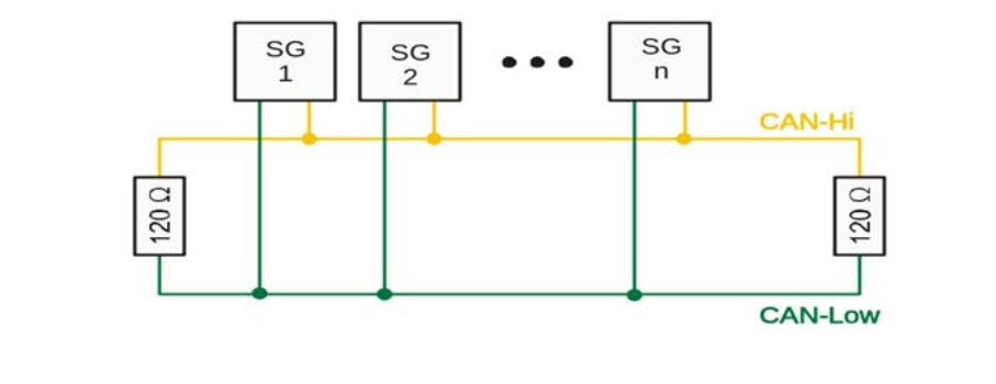
The CB1, CB2 and CB3 CANBus modules conform to the standard CANBus architecture. As applications may require many nodes (such as the strain gauges [SG] shown in the example), which are not predetermined, the CB1/CB2/CB3 channel(s) are not provided with any bus termination. Proper bus termination is dependent on the end-use application. 120 ohm resistors must be applied to each end of the CANBus – this termination is required for proper operation and must be provided or applied externally to the CB1/CB2/CB3 module channel(s). The figure below shows an example of CANBus terminations.
Built-In Test (BIT)/Diagnostic Capability
Built-In Test (BIT) is invoked at power on and then can be manually invoked on demand by setting a bit in the Control register for each channel, which forces BIT to be run for the given channel. When running BIT, the CANBus module will be taken out of “Normal” mode and temporarily placed in “Loopback” mode. When BIT finishes, CANBus will be placed back into Normal mode. While in Loopback mode, CANBus will not respond to receive or transmit requests. A specific CAN test message is sent, received and verified for each of the CAN channels while in loopback mode. The BIT status register is updated to reflect whether each channel passed. Each bit in the BIT status register indicates a channel starting with bit zero for channel 1, bit 1 for channel 2 etc. A value of 0 indicates BIT passes for that channel and a value of 1 indicates failure.
Status and Interrupts
The CANBus Module provides registers that indicate faults or events. Refer to “Status and Interrupts Module Manual” for the Principle of Operation description.
Module Common Registers
The CANBus Module includes module common registers that provide access to module-level bare metal/FPGA revisions & compile times, unique serial number information, and temperature/voltage/current monitoring. Refer to “Module Common Registers Module Manual” for the detailed information.
REGISTER DESCRIPTIONS
The register descriptions provide the register name, Register Offset, Type, Data Range, Read or Write information, Default Value, a description of the function and, in most cases, a data table.
Note
Unless otherwise noted, the descriptions are applicable to CB1, CB2 and CB3.
Receive Registers
The registers listed are associated with data that is received on the CANBus channels.
Receive FIFO Buffer Data
Function: Stores received messages.
Type: unsigned binary word (32-bit)
Data Range: 0x0000 0000 to 0x00FF FFFF
Read/Write: R
Operational Settings: NA
Initialized Value: 0
Receive FIFO Word Count
Function: Contains the number of words in the Receive FIFO buffer.
Type: unsigned integer word
Data Range: 0 to 1048576 (0 to 0x0010 0000)
Read/Write: R
Operational Settings: NA
Initialized Value: 0
Receive FIFO Frame Count
Function: Contains the number of frames in the Receive FIFO buffer.
Type: unsigned integer word
Data Range: 0 to 209715 (0 to 0x0003 3333) (Minimum CAN frame will be 5 entries on the FIFO)
Read/Write: R
Operational Settings: Each minimum CAN frame is 5; 32-bit words that get placed on the FIFO. Maximum frame count is thus 1048576 (0x0010 0000) / 5 = 209715 (0x0003 3333).
Initialized Value: 0
Receive FIFO Threshold Registers
The Receive FIFO Almost Full, Receive FIFO High Watermark, and Receive FIFO Buffer Low Watermark sets the threshold limits that are used to set the bits in the Receive FIFO Status register.
Receive FIFO Buffer Almost Full
Function: Specifies the maximum size of the Receive Buffer before the RxFIFO Almost Full Status bit D0 in the FIFO Status register is flagged (High True).
Type: unsigned integer
Data Range: 0 to 1048576 (0 to 0x0010 0000)
Read/Write: R/W
Operational Settings: NA
Initialized Value: 0
Receive FIFO Buffer High Watermark
Function: Defines the Receive Buffer High Watermark value.
Type: binary word (32-bit)
Data Range: Low Watermark < High Watermark < 1048576 (0x0010 0000)
Read/Write: R/W
Operational Settings: When Rx Buffer size equals the High Watermark value, FIFO Status bit D3 is flagged.
Initialized Value: 0
Receive FIFO Buffer Low Watermark
Function: Defines the Receive Buffer Low Watermark value.
Type: unsigned binary word (32-bit)
Data Range: 0 < Low Watermark < High Watermark < 1048576 (0x0010 0000)
Read/Write: R/W
Operational Settings: When the Rx Buffer size is less than the Low Watermark value, FIFO Status bit D3 is flagged.
Initialized Value: 0
Transmit Registers
The registers listed are associated with data that is transmitted on the CANBus channels.
Transmit FIFO Buffer Data
Function: Transmits messages in FIFO
Type: unsigned binary word (32-bit)
Data Range: 0x0000 0000 to 0x00FF FFFF
Read/Write: W
Operational Settings: NA
Initialized Value: 0
Transmit FIFO Word Count
Function: Contains the number of words in the Transmit FIFO register.
Type: unsigned integer word
Data Range: 0 to 1048576 (0 to 0x0010 0000)
Read/Write: R
Operational Settings: NA
Initialized Value: 0
Transmit FIFO Frame Count
Function: Contains the number of frames in the Transmit FIFO register.
Type: unsigned integer word
Data Range: 0 to 209715 (0 to 0x0003 3333) (Minimum CAN frame will be 5 entries on the FIFO)
Read/Write: R
Operational Settings: Each minimum CAN frame is 5; 32-bit words that get placed on the FIFO. Maximum frame count is thus 1048576 (0x0010 0000) / 5 = 209715 (0x0003 3333).
Initialized Value: 0
Transmit FIFO Threshold Registers
Transmit FIFO Buffer Almost Empty
Function: Specifies the minimum size of the Transmit FIFO register, before the Tx FIFO Almost Empty Status bit D1 in the FIFO Status register is flagged (High True).
Type: unsigned integer
Data Range: 0 to 1048576 (0 to 0x0010 0000)
Read/Write: R/W
Operational Settings: NA
Initialized Value: 0
Control Registers
The registers specified in this section provide the ability to configure the Baud/Bit Timing, J1939 Source Address, Protocol Assignment, and control the operation for each CANBus channel.
Baud/Bit Timing
Function: Configures baud and bit timing points.
Type: unsigned binary word (32-bit)
Data Range: 0, 1
Read/Write: R/W
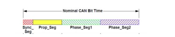
Operational Settings: Per the CAN specification, the bit time is divided into four segments: The Synchronization Segment, the Propagation Time Segment, the Phase Buffer Segment 1, and the Phase Buffer Segment 2. Each segment consists of a specific, programmable number of time quanta. The length of the time quantum (tq), which is the basic time unit of the bit time, is defined by the CAN controller’s system clock frequency fpclk and the Baud Rate Prescaler (BRP): tq = BRP / 8 MHz. The time, the Baud Rate Prescaler and the Baud Rate Prescaler extension are used to divide down he internal 8 MHz clock.
Initialized Value: 0
Note
Changing baud/timing settings while a message is transmitting will cause that message to be stopped.
Baud/Bit Timing
| D31 | D30 | D29 | D28 | D27 | D26 | D25 | D24 | D23 | D22 | D21 | D20 | D19 | D18 | D17 | D16 |
|---|---|---|---|---|---|---|---|---|---|---|---|---|---|---|---|
| D | D | D | D | D | D | D | D | D | D | D | D | D | D | D | D |
| D15 | D14 | D13 | D12 | D11 | D10 | D9 | D8 | D7 | D6 | D5 | D4 | D3 | D2 | D1 | D0 |
| 0 | 0 | 0 | 0 | 0 | 0 | 0 | 0 | 0 | 0 | 0 | 0 | 0 | 0 | 0 | 0 |
| Bit | Description |
|---|---|
| D31 | Assert new settings. Writing a 1 will cause the channel to reset and restart with the Baud/Bit timing settings in this register. This bit will return to 0 after the setting has taken effect. |
| D30:28 | TSeg2: The time segment after the sample point. 0x0 to 0x7 are valid values. |
| D27:24 | TSeg1: The time segment before the sample point. 0x1 to 0xF are valid values. |
| D23:22 | SJW: (Re) Synchronization Jump Width. 0x0-0x3 are valid programmed values. The actual interpretation by the hardware of this value is such that one more than the value programmed here is used. |
| D21:16 | BRP: Baud Rate Prescaler. 0x00-0x3F are valid values. The value by which he oscillator frequency is divided for generating the bit time quanta. The bit time is built up from a multiple of this quanta. Valid values for the Baud Rate Prescaler are [0…63]. The actual interpretation by the hardware of this value is such that one more than the value programmed here is used. |
| D15:D0 | 0 |
The CAN bit time may be programmed in the range of [4 …
25] time quanta.
The CAN time quantum may be programmed in the range of [1 …
1024] CAN_CLK periods.
The actual interpretation by the hardware of this value is such that one
more than the value programmed here is used.
TSeg1 is the sum of Prop_Seg and Phase_Seg1.
TSeg2 is Phase_Seg2.
Therefore, the length of the bit time is (programmed values) [TSeg1 + TSeg2
3] tq or (functional values) [Sync_Seg Prop_Seg + Phase_Seg1
Phase_Seg2] tq.
Example: 1 MHz CANBus Bit Sample Time / Baud rate programming calculation(s)
Module channel(s) are based on 8 MHz clock; 125 ns is the quantum:
The bit time is defined as: Tbit = TSeg1 TSeg2 3
For programming 1 MHz data rate (1usec) we need 8 quanta, so the pre-scaler register is set to (0). The actual pre-scaler value is one more than the register value or 1:
8(quantum) = TSeg1 TSeg2 3(quantum) or 5(quantum) = TSeg1 + TSeg2
The Sync_Seq is defined by the specification as 1(quantum), so, to center sample the CAN bit, the center would be at 4(quantum):
4(quantum) = 1(quantum) + TSeg1 or TSeg1 = 3(quantum)
Therefore, for 1 MHz baud rate, the time segment timing register bits should be set as follows:
PRESCALER = 0
TSEG1 = 3
TSEG2 = 2
Note
The sample point can be ‘moved/adjusted’ for system(s) known to have a long rise time or propagation delay.
However, the relationship 5(quantum) = TSeg1 + TSeg2 must be maintained.
Control
(Firmware Version 1.12 and older, prior to 6/15/2017)
Function: Provides flags for controlling transmit and receive activity.
Type: unsigned binary word (32-bit)
Data Range: 0x0000 0000 to 0x00FF FFFF
Read/Write: R/W
Operational Settings: See descriptions that follow.
Initialized Value: 0
Control
| D31 | D30 | D29 | D28 | D27 | D26 | D25 | D24 | D23 | D22 | D21 | D20 | D19 | D18 | D17 | D16 |
|---|---|---|---|---|---|---|---|---|---|---|---|---|---|---|---|
| 0 | 0 | 0 | 0 | 0 | 0 | 0 | 0 | 0 | 0 | 0 | 0 | 0 | 0 | 0 | 0 |
| D15 | D14 | D13 | D12 | D11 | D10 | D9 | D8 | D7 | D6 | D5 | D4 | D3 | D2 | D1 | D0 |
| D | D | D | D | 0 | 0 | 0 | 0 | 0 | 0 | D | D | 0 | D | 0 | D |
| Bit | Description |
|---|---|
| D0 | Enable transmit. When set to 1: transmit any complete frames loaded into the Tx FIFO. When set to 0, transmission is held off and the queued data in the FIFO held until set to 1. |
| D2 | Enable receive. When set to 1: enables channel to receive data from CAN bus to Rx FIFO. |
| D4 | Enable CANBus 2.0 A/B Protocol* - if a request to change a channel protocol is made and the channel was not already assigned to the desired protocol, the CAN channel is reset to the default baud rate timing parameters of the specified protocol, all status for the channel is cleared but Rx and Tx transmissions are NOT disabled - they retain their current state. |
| D5 | Enable J1939 Protocol* - if a request to change a channel protocol is made and the channel was not already assigned to the desired protocol, the CAN channel is reset to the default baud rate timing parameters of the specified protocol, all status for the channel is cleared but Rx and Tx transmissions are NOT disabled - they retain their current state. |
| D12 | Retrieve Address (J1939 only): Indicates a request to retrieve the address currently assigned to the CAN channel. This is a control bit indicating the request to retrieve the address assigned to the CAN channel. When the CAN module detects the request, it will populate the Source Address Register with currently assigned address. See Source Address register. Set per channel. |
| D13 | Assign Address (J1939 only): Indicates that a specific address is to be assigned to this CAN channel. This is just a control bit indicating a request is being made to set the address. Caller must also write the actual address to be assigned to the specific channel’s Source Address register. See Source Address register. Set per channel. |
| D14 | BIT. Forces Built-In-Test to be run for the given channel. Note: when running BIT, the CANBus module will be taken out of “Normal” mode and temporarily placed in “Loopback” mode. When BIT finishes, CANBus will be placed back into Normal mode. While in Loopback mode, CANBus will not respond to receive or transmit requests. |
| D15 | Reset Channel. Clears receive and transmit FIFOs for the channel, disables both Rx and Tx transmissions, clears all status, and reinitializes the channel with the last configured baud rate timing parameters. NOTE: both, baud rate timing and assigned protocol retain their current values when a channel reset is performed. If the channel is in the Bus Off state, this reset initiates a recovery sequence. Once a recovery sequence has started, the device will wait for 129 occurrences of Bus Idle before resuming normal operations. At the end of the Bus Off recovery cycle, the Error Management Counters will be reset. |
| * | Only active for CB3. Select desired protocol for each channel. |
(Firmware Version 1.13, NAIbrd Version 1.44 and later, from 6/20/2017 and on)
Rationale for Control Register changes: The control register has been modified to act solely as a “request for action” register. Bits can be set to a 1 to request various actions or capabilities. When the action or capability is acted upon by the CAN firmware, these request bits will be set back to 0. Unlike the functionality of the Control Register of previous versions, this control register does not retain any state. States such as whether TX or RX is enabled or the protocol that a specific channel is assigned to, are now kept in dedicated registers. (see the Register Map).
Function: Provides flags for controlling transmit and receive activity.
Type: binary word (32-bit)
Data Range: 0x0000 0000 to 0x00FF FFFF
Read/Write: R/W
Operational Settings: See descriptions that follow.
Initialized Value: 0
Control
| D31 | D30 | D29 | D28 | D27 | D26 | D25 | D24 | D23 | D22 | D21 | D20 | D19 | D18 | D17 | D16 |
|---|---|---|---|---|---|---|---|---|---|---|---|---|---|---|---|
| D | 0 | 0 | 0 | 0 | 0 | 0 | 0 | 0 | 0 | 0 | 0 | 0 | 0 | 0 | 0 |
| D15 | D14 | D13 | D12 | D11 | D10 | D9 | D8 | D7 | D6 | D5 | D4 | D3 | D2 | D1 | D0 |
| D | D | D | D | D | D | D | D | 0 | 0 | D | D | D | D | D | D |
| Bit | Description |
|---|---|
| D0 | Enable transmit. When set to 1: transmit any complete frames loaded into the Tx FIFO. |
| D1 | Disable transmit. When set to 1: transmission is held off and the queued data in the FIFO held until the enable transmit bit is set to a 1. |
| D2 | Enable receive. When set to 1: enables channel to receive data from CAN bus to Rx FIFO. |
| D3 | Disable receive. When set to 1: disables channel from receiving data from CAN bus to Rx FIFO. |
| D4 | Enable CANBus 2.0 A/B Protocol* - if a request to change a channel protocol is made and the channel was not already assigned to the desired protocol, the CAN channel is reset to the default baud rate timing parameters of the specified protocol, all status for the channel is cleared but Rx and Tx transmissions are NOT disabled - they retain their current state. |
| D5 | Enable J1939 Protocol* - if a request to change a channel protocol is made and the channel was not already assigned to the desired protocol, the CAN channel is reset to the default baud rate timing parameters of the specified protocol, all status for the channel is cleared but Rx and Tx transmissions are NOT disabled - they retain their current state. |
| D8 | Request Bit Timing |
| D9 | Baud Rate change (predefined baud rates) |
| D10 | Request reset of Rx FIFO |
| D11 | Request reset of Tx FIFO |
| D12 | Retrieve Address (J1939 only): Indicates a request to retrieve the address currently assigned to the CAN channel. This is a control bit indicating the request to retrieve the address assigned to the CAN channel. When the CAN module detects the request, it will populate the Source Address Register with currently assigned address. See Source Address register. Set per channel. |
| D13 | Assign Address (J1939 only): Indicates that a specific address is to be assigned to this CAN channel. This is just a control bit indicating a request is being made to set the address. Caller must also write the actual address to be assigned to the specific channel’s Source Address register. See Source Address register. Set per channel. |
| D14 | BIT. Forces Built-In-Test to be run for the given channel. Note: when running BIT, the CANBus module will be taken out of “Normal” mode and temporarily placed in “Loopback” mode. When BIT finishes, CANBus will be placed back into Normal mode. While in Loopback mode, CANBus will not respond to receive or transmit requests. |
| D15 | Reset Channel. Clears receive and transmit FIFOs for the channel, disables both Rx and Tx transmissions, clears all status, and reinitializes the channel with the last configured baud rate timing parameters. NOTE: both, baud rate timing and assigned protocol retain their current values when a channel reset is performed. If the channel is in the Bus Off state, this reset initiates a recovery sequence. Once a recovery sequence has started, the device will wait for 129 occurrences of Bus Idle before resuming normal operations. At the end of the Bus Off recovery cycle, the Error Management Counters will be reset. |
| D31 | Config Edit. Set to a 1 to indicate baremetal application to hold off processing any command requests until this bit is set back to a zero. |
| * | Only active for CB3. Select desired protocol for each channel. |
Source Address (J1939 Only)
Function: Defines/Reflects the J1939 source address (channel based)
Type: unsigned binary word (32-bit)
Data Range: 0 - 253
Read/Write: R/W
Operational Settings: Each J1939 channel can be assigned an address from 0
- 253 inclusive. Care should be taken when choosing J1939 addresses - Industry specific reserved address range is typically from 208-247and the industry specific dynamic range is typically 128 - 207. When attempting to claim a source address, make sure both TX and RX are enabled on all channels that have J1939 devices attached for addresses to successfully be claimed. Once claimed, you may disable TX and RX until such time you want the device(s) to be active.
Initialized Value: 0
Source Address (J1939)
| D31 | D30 | D29 | D28 | D27 | D26 | D25 | D24 | D23 | D22 | D21 | D20 | D19 | D18 | D17 | D16 |
|---|---|---|---|---|---|---|---|---|---|---|---|---|---|---|---|
| D | 0 | 0 | 0 | 0 | 0 | 0 | 0 | 0 | 0 | 0 | 0 | 0 | 0 | 0 | 0 |
| D15 | D14 | D13 | D12 | D11 | D10 | D9 | D8 | D7 | D6 | D5 | D4 | D3 | D2 | D1 | D0 |
| 0 | 0 | 0 | 0 | 0 | 0 | 0 | 0 | D | D | D | D | D | D | D | D |
Protocol Assignment (CB3 Only)
(Firmware Version 1.13, NAIbrd Version 1.44 and later, from 6/20/2017 and on)
Function: Defines/Reflects the assigned protocol - CAN A/B or CAN J1939 (channel based)
Type: unsigned binary word (32-bit)
Data Range: 16 (0x10) CAN A/B or 32 (0x20) CAN J1939
Read/Write: R/W
Operational Settings: Each channel register will either reflect 0x10 for CAN A/B or 0x20 for CAN J1939.
Initialized Value: 0x20
Protocol Assignment (CB3 Only)
| D31 | D30 | D29 | D28 | D27 | D26 | D25 | D24 | D23 | D22 | D21 | D20 | D19 | D18 | D17 | D16 |
|---|---|---|---|---|---|---|---|---|---|---|---|---|---|---|---|
| D | 0 | 0 | 0 | 0 | 0 | 0 | 0 | 0 | 0 | 0 | 0 | 0 | 0 | 0 | 0 |
| D15 | D14 | D13 | D12 | D11 | D10 | D9 | D8 | D7 | D6 | D5 | D4 | D3 | D2 | D1 | D0 |
| 0 | 0 | 0 | 0 | 0 | 0 | 0 | 0 | 0 | 0 | D | D | 0 | 0 | 0 | 0 |
| Bit | Description |
|---|---|
| D4 | CAN A/B |
| D5 | CAN J1939 |
Transmit/Receive Enable State
(Firmware Version 1.13, NAIbrd Version 1.44 and later, from 6/20/2017 and on)
Function: Reflects the state of Transmit Enable and Receive Enable
Type: unsigned binary word (32-bit)
Data Range:
Read/Write: R/W
Operational Settings: See below.
Initialized Value: 0
Transmit/Receive Enable State
| D31 | D30 | D29 | D28 | D27 | D26 | D25 | D24 | D23 | D22 | D21 | D20 | D19 | D18 | D17 | D16 |
|---|---|---|---|---|---|---|---|---|---|---|---|---|---|---|---|
| D | 0 | 0 | 0 | 0 | 0 | 0 | 0 | 0 | 0 | 0 | 0 | 0 | 0 | 0 | 0 |
| D15 | D14 | D13 | D12 | D11 | D10 | D9 | D8 | D7 | D6 | D5 | D4 | D3 | D2 | D1 | D0 |
| 0 | 0 | 0 | 0 | 0 | 0 | 0 | 0 | 0 | 0 | 0 | 0 | 0 | D | 0 | D |
| Bit | Description |
|---|---|
| D0 | TX Enabled when bit reflects a 1. |
| D2 | RX Enabled when bit reflects a 1. |
Message Status/Monitoring Registers
The registers specified in this section provide status and monitoring information on about the CANBus messages.
FIFO Status
Function: Describes current FIFO Status.
Type: unsigned binary word (32-bit)
Data Range: NA
Read/Write: R
Operational Settings: See Receive Buffer Almost Full, Transmit Buffer Almost Empty, Receive Buffer High Watermark and Receive Buffer Low Watermark specific registers for function description and programming.
Initialized Value: 0
| Bit | Description | Configurable? |
|---|---|---|
| D0 | Rx FIFO ALMOST FULL: 1 when FIFO Word Count >= “Receive FIFO Buffer Almost Full” register | Yes |
| D1 | Tx FIFO ALMOST EMPTY: 1 when FIFO Word Count ⇐ “Transmit FIFO Buffer Almost Empty” register | Yes |
| D2 | HIGH WATERMARK REACHED: 1 wen FIFO Word Count >= “Receive FIFO Buffer High Watermark” register | Yes |
| D3 | LOW WATERMARK REACHED: 1 when FIFO Word Count ⇐ “Receive FIFO Buffer Low Watermark” register | Yes |
| D4 | Rx EMPTY: 1 when FIFO Word Count = 0 | No |
| D5 | Tx FULL: 1 when FIFO Word Count = 65536 | No |
Last Error Code (LEC)
Function: Provides error status information for Bus Status register, Comm Status register and Core Status register.
Type: unsigned binary word (32-bit)
Data Range: 0 to 3
Read/Write: R
Operational Settings: The last error code to be received on a channel. Reading resets this register to 0.
Initialized Value: 0
Last Error Code (LEC)
| D31 | D30 | D29 | D28 | D27 | D26 | D25 | D24 | D23 | D22 | D21 | D20 | D19 | D18 | D17 | D16 |
|---|---|---|---|---|---|---|---|---|---|---|---|---|---|---|---|
| D | 0 | 0 | 0 | 0 | 0 | 0 | 0 | 0 | 0 | 0 | 0 | 0 | 0 | 0 | 0 |
| D15 | D14 | D13 | D12 | D11 | D10 | D9 | D8 | D7 | D6 | D5 | D4 | D3 | D2 | D1 | D0 |
| 0 | 0 | 0 | 0 | 0 | 0 | 0 | 0 | 0 | 0 | 0 | 0 | 0 | 0 | D | D |
| Bit | Description |
|---|---|
| D0 | Bus Status error. When set to a 1, user is directed to look at the Bus Status register. 0 indicates no error. |
| D1 | Comm Status error. When set to a 1, user is directed to look at the Comm Status register. 0 indicates no error. |
Bus Status
Function: Provides bus status for each channel. Indicates the type of error that has occurred on the bus.
Type: unsigned binary word (32-bit)
Data Range: 0x0000 0000 to 0x00FF FFFF
Read/Write: R/W
Operational Settings: 0 = No error detected. 1 = Error detected.
Initialized Value: 0
Bus Status
| D31 | D30 | D29 | D28 | D27 | D26 | D25 | D24 | D23 | D22 | D21 | D20 | D19 | D18 | D17 | D16 |
|---|---|---|---|---|---|---|---|---|---|---|---|---|---|---|---|
| D | 0 | 0 | 0 | 0 | 0 | 0 | 0 | 0 | 0 | 0 | 0 | 0 | 0 | 0 | 0 |
| D15 | D14 | D13 | D12 | D11 | D10 | D9 | D8 | D7 | D6 | D5 | D4 | D3 | D2 | D1 | D0 |
| 0 | 0 | 0 | 0 | 0 | 0 | 0 | 0 | 0 | 0 | 0 | D | D | D | D | D |
| Bit | Description |
|---|---|
| D31:D5 | 0 |
| D4 | ACKERR - ACK Error - Indicates acknowledgement error. Write to clear. |
| D3 | BERR - Bit Error - Indicates the received bit is not the same as the transmitted bit during bus communication. Write to clear. |
| D2 | STER - Stuff Error - Indicates an error if there is a stuffing violation. Write to clear. |
| D1 | FMER - Form Error - Indicates an error in one of the fixed form fields in the message frame. Write to clear. |
| D0 | CRCER - CRC Error - Indicates a CRC error has occurred. Write to clear. |
Comm Status
Function: Provides communication status for each channel.
Type: unsigned binary word (32-bit)
Data Range: 0x0000 0000 to 0x00FF FFFF
Read/Write: R
Operational Settings: Communication status values are actual numeric values comprising of one or more register bits being set.
Initialized Value: 0
Communication Status
| D31 | D30 | D29 | D28 | D27 | D26 | D25 | D24 | D23 | D22 | D21 | D20 | D19 | D18 | D17 | D16 |
|---|---|---|---|---|---|---|---|---|---|---|---|---|---|---|---|
| D | 0 | 0 | 0 | 0 | 0 | 0 | 0 | 0 | 0 | 0 | 0 | 0 | 0 | 0 | 0 |
| D15 | D14 | D13 | D12 | D11 | D10 | D9 | D8 | D7 | D6 | D5 | D4 | D3 | D2 | D1 | D0 |
| 0 | 0 | 0 | 0 | 0 | 0 | 0 | 0 | 0 | 0 | 0 | 0 | D | D | D | D |
D31:4 = 0 (not used)
| Comm Status | Value | Bits |
|---|---|---|
| FIFO Empty | 0x0001 (1) | D0 |
| FIFO Not Enough Data | 0x0002 (2) | D1 |
| FIFO Start Flag Not Found | 0x0003 (3) | D1, D0 |
| FIFO Transmit Data Count Null | 0x0004 (4) | D2 |
| FIFO End Flag Not Found | 0x0005 (5) | D2, D0 |
| Bad Size | 0x0006 (6) | D2, D1 |
| Not in Configuration Mode | 0x0007 (7) | D2, D1, D0 |
| Transmit Failure | 0x0008 (8) | D3 |
| Source Address in Use | 0x0009 (9) | D3, D0 |
| FIFO Full | 0x000A (10) | D3, D1 |
| Receive Failure | 0x000B (11) | D3, D1, D0 |
| Baud Configuration Failure | 0x000C (12) | D3, D2 |
Core Status
Function: Provides core status for each channel.
Type: unsigned binary word (32-bit)
Data Range: 0x0000 0000 to 0x00FF FFFF
Read/Write: R
Operational Settings: 0 = No error detected. 1 = Error detected.
Initialized Value: 0
Core Status
| D31 | D30 | D29 | D28 | D27 | D26 | D25 | D24 | D23 | D22 | D21 | D20 | D19 | D18 | D17 | D16 |
|---|---|---|---|---|---|---|---|---|---|---|---|---|---|---|---|
| D | 0 | 0 | 0 | 0 | 0 | 0 | 0 | 0 | 0 | 0 | 0 | 0 | 0 | 0 | 0 |
| D15 | D14 | D13 | D12 | D11 | D10 | D9 | D8 | D7 | D6 | D5 | D4 | D3 | D2 | D1 | D0 |
| 0 | 0 | 0 | 0 | D | D | D | D | D | D | D | D | D | D | D | D |
| Bits | Description |
|---|---|
| D31:12 | 0 |
| D11 | ACFBSY - Acceptance Filter Busy. Indicates that the Acceptance Mask/Priority registers and the Acceptance Code/Address registers cannot be written to. 1 = Acceptance Mask/Priority registers and Acceptance Code/Address registers cannot be written to. 0 = Acceptance Mask/Priority registers and the Acceptance Code/Address registers can be written to. |
| D10 | TXFLL - Transmit FIFO Full. Indicates that the Tx FIFO is full. 1 = Indicates the TX FIFO is full. 0 = Indicates the TX FIFO is not full. |
| D9 | TXBFLL - High Priority Transmit Buffer Full. Indicates the High Priority Transmit Buffer is full. 1 = Indicates the High Priority Transmit Buffer is full. 0 = Indicates the High Priority Transmit Buffer is not full. |
| D8:D7 | ESTAT [1..0] - Error Status. Indicates the error status of the CAN core. 00 = Indicates Configuration Mode (CONFIG = 1). Error State is undefined. 01 = Indicates Error Active State. 11 = Indicates Error Passive State. 10 = Indicates Bus Off State. |
| D6 | ERRWRN - Error Warning. Indicates that either the Transmit Error counter or the Receive Error counter has exceeded a value of 96. 1 = One or more error counters have a value ≥ 96. 0 = Neither of the error counters has a value ≥ 96. |
| D5 | BBSY - Bus Busy. Indicates the CAN bus status. 1 = Indicates that the CAN core is either receiving a message or transmitting a message. 0 = Indicates that the CAN core is either in Configuration mode or the bus is idle. |
| D4 | BIDLE - Bus Idle. Indicates the CAN bus status. 1 = Indicates no bus communication is taking place. 0 = Indicates the CAN core is either in Configuration mode or the bus is busy. |
| D3 | NORMAL - Normal Mode. Indicates the CAN core is in Normal Mode. 1 = Indicates the CAN core is in Normal Mode. 0 = Indicates the CAN core is not in Normal mode. |
| D2 | SLEEP - Sleep Mode. Indicates the CAN core is in Sleep mode. 1 = Indicates the CAN core is in Sleep mode. 0 = Indicates the CAN core is not in Sleep mode. |
| D1 | LBACK - Loopback Mode. Indicates the CAN core is in Loopback mode. 1 = Indicates the CAN core is in Loopback mode. 0 = Indicates the CAN core is not in Loopback mode. |
| D0 | CONFIG - Configuration Mode Indicator. Indicates the CAN core is in Configuration mode. 1 = Indicates the CAN core is in Configuration mode. 0 = Indicates the CAN core is not in Configuration mode. |
Transmit/Receive Error Counter
Function: Detects transmit and receive errors at the physical layer.
Type: unsigned binary word (32-bit)
Data Range: 0x0000 0000 to 0x00FF FFFF
Read/Write: R
Operational Settings: 0 = The Receive or Transmit Error Counter is below the error passive level. 1 = The Receive or Transmit Error Counter has reached the error passive level as defined in the CAN Specification.
Initialized Value: 0
Transmit/Receive Error Count
| D31 | D30 | D29 | D28 | D27 | D26 | D25 | D24 | D23 | D22 | D21 | D20 | D19 | D18 | D17 | D16 |
|---|---|---|---|---|---|---|---|---|---|---|---|---|---|---|---|
| D | 0 | 0 | 0 | 0 | 0 | 0 | 0 | 0 | 0 | 0 | 0 | 0 | 0 | 0 | 0 |
| D15 | D14 | D13 | D12 | D11 | D10 | D9 | D8 | D7 | D6 | D5 | D4 | D3 | D2 | D1 | D0 |
| D | D | D | D | D | D | D | D | D | D | D | D | D | D | D | D |
| Bits | Description |
|---|---|
| D31:D16 | 0 |
| D15 | 1 = Error Passive State 0 = Error Active State |
| D14:D8 | REC (7 Bits): Receive Error Counter. Actual state of Receive Error Counter. Values between 0 & 127. |
| D7:D0 | TEC (8 Bits): Transmit Error Counter. Actual state of Transmit Error Counter. Values between 0 & 255 |
Drop Count
Function: Keeps track of how many received CAN messages were dropped since power on.
Type: unsigned binary word (32-bit)
Data Range: 0x0000 0000 to 0xFFFF FFFF
Read/Write: R
Operational Settings: If an incoming CAN message is unable to fit in the Receive FIFO register, the message is dropped. This register indicates whether CAN messages are getting dropped.
Initialized Value: 0
CANBus Filtering Registers
CANBus Filtering is comprised of a maximum of 4 separate CANBus filters. Each CANBus filter is made up of a pair of 32-bit value registers: an Acceptance Mask and an Acceptance Code. The number of enabled acceptance filters is governed by the first 3 bits of the Filter Control register. Valid values are from 0 (no filtering) to 4 (maximum filtering where all 4 Acceptance Filters are enabled). Acceptance Filtering is performed in this sequence:
- The incoming CAN Identifier is masked with the bits in the Acceptance Filter Mask register.
- The Acceptance Filter Code register is also masked with the bits in the Acceptance Filter Mask register.
- Both resulting values are compared.
- If both these values are equal, then the CAN message is stored in the Receive FIFO register.
- Acceptance filtering is processed by each of the enabled defined filters. If the incoming CAN identifier passes through any acceptance filter, then the message is stored in the Receive FIFO register.
Filter Control
Function: Controls which Acceptance Filters are enabled and provides for a means for users to customize CAN filtering. Each channel has a maximum of 4 acceptance filter mask and code pairs that can be configured and enabled.
Type: unsigned binary word (32-bit)
Data Range: 0x0000 0000 to 0xFFFF FFFF
Read/Write: R/W
Operational Settings: See descriptions below.
Initialized Value: 0
Definitions:
RTR = Remote Transmission Request
IDE = Identifier Extension Mask
SRR = Substitute Remote Transmission Request
| Bits | Description |
|---|---|
| D31 | Acceptance Filter #4 RTR value (Note: This bit is only taken into account if the Enable RTR bit (Bit 28) is set to 1) 0 = no remote transmission requests will be accepted 1 = indicates only remote transmission requests will be accepted |
| D30 | Acceptance Filter #4 SRR value (Note: This bit is only taken into account if the Enable SRR bit (Bit 27) is set to 1) 0 = no substitute remote transmission requests will be accepted 1 = only substitute remote transmission requests will be accepted |
| D29 | Acceptance Filter #4 Standard/Extended value (Note: This bit is only taken into account if the Enable A/B Filter bit (Bit 26) is set to 1) 0 = only accept standard frames 1 = only accept extended frames |
| D28 | Acceptance Filter #4 Enable RTR Filter 0 = do not take RTR into account when filtering 1 = do take RTR value into account when filtering - look at Bit 31 for acceptance value |
| D27 | Acceptance Filter #4 Enable SRR Filter 0 = do not take SRR into account when filtering 1 = do take SRR value into account when filtering - look at Bit 30 for acceptance value |
| D26 | Acceptance Filter #4 Enable Standard/Extended Filter 0 = do not take Standard/Extended into account when filtering 1 = do take Standard/Extended into account when filtering - look at Bit 29 for acceptance value |
| D25 | Acceptance Filter #4 Enable Acceptance Code and Mask 0 = do not enable the acceptance code and mask (user does not want to filter by CAN ID) 1 = do enable the acceptance code and mask (user wants to filter by CAN ID as well) |
| D24 | Acceptance Filter #3 RTR value (Note: This bit is only considered if the Enable RTR bit (Bit 21) is set to 1) 0 = no remote transmission requests will be accepted 1 = indicates only remote transmission requests will be accepted |
| D23 | Acceptance Filter #3 SRR value (Note: This bit is only considered if the Enable SRR bit (Bit 20) is set to 1) 0 = no substitute remote transmission requests will be accepted 1 = only substitute remote transmission requests will be accepted |
| D22 | Acceptance Filter #3 Standard/Extended value (Note: This bit is only considered if the Enable A/B Filter bit (Bit 19) is set to 1) 0 = only accept standard frames 1 = only accept extended frames |
| D21 | Acceptance Filter #3 Enable RTR Filter 0 = do not take RTR into account when filtering 1 = do take RTR value into account when filtering - look at Bit 24 for acceptance value |
| D20 | Acceptance Filter #3 Enable SRR Filter 0 = do not take SRR into account when filtering 1 = do take SRR value into account when filtering - look at Bit 23 for acceptance value |
| D19 | Acceptance Filter #3 Enable Standard/Extended Filter 0 = do not take Standard/Extended into account when filtering 1 = do take Standard/Extended into account when filtering - look at Bit 22 for acceptance value |
| D18 | Acceptance Filter #3 Enable Acceptance Code and Mask 0 = do not enable the acceptance code and mask (user does not want to filter by CAN ID) 1 = do enable the acceptance code and mask (user wants to filter by CAN ID as well) |
| D17 | Acceptance Filter #2 RTR value (Note: This bit is only taken into account if the Enable RTR bit (Bit 14) is set to 1) 0 = no remote transmission requests will be accepted 1 = indicates only remote transmission requests will be accepted |
| D16 | Acceptance Filter #2 SRR value (Note: This bit is only considered if the Enable SRR bit (Bit 13) is set to 1) 0 = no substitute remote transmission requests will be accepted 1 = only substitute remote transmission requests will be accepted |
| D15 | Acceptance Filter #2 Standard/Extended value (Note: This bit is only considered if the Enable A/B Filter bit (BIT 12) is set to 1) 0 = only accept standard frames 1 = only accept extended frames |
| D14 | Acceptance Filter #2 Enable RTR Filter 0 = do not take RTR into account when filtering 1 = do take RTR value into account when filtering - look at Bit 17 for acceptance value |
| D13 | Acceptance Filter #2 Enable SRR Filter 0 = do not take SRR into account when filtering 1 = do take SRR value into account when filtering - look at Bit 16 for acceptance value |
| D12 | Acceptance Filter #2 Enable Standard/Extended Filter 0 = do not take Standard/Extended into account when filtering 1 = do take Standard/Extended into account when filtering - look at Bit 15 for acceptance value |
| D11 | Acceptance Filter #2 Enable Acceptance Code and Mask 0 = do not enable the acceptance code and mask (user does not want to filter by CAN ID) 1 = do enable the acceptance code and mask (user wants to filter by CAN ID as well) |
| D10 | Acceptance Filter #1 RTR value (Note: This bit is only considered if the Enable RTR bit (Bit 7) is set to 1) 0 = no remote transmission requests will be accepted 1 = indicates only remote transmission requests will be accepted |
| D9 | Acceptance Filter #1 SRR value (Note: This bit is only considered if the Enable SRR bit (Bit 6) is set to 1) 0 = no substitute remote transmission requests will be accepted 1 = only substitute remote transmission requests will be accepted |
| D8 | Acceptance Filter #1 Standard/Extended value (Note: This bit is only considered if the Enable A/B Filter bit (Bit 5) is set to 1) 0 = only accept standard frames 1 = only accept extended frames |
| D7 | Acceptance Filter #1 Enable RTR Filter 0 = do not take RTR into account when filtering 1 = do take RTR value into account when filtering - look at Bit 10 for acceptance value |
| D6 | Acceptance Filter #1 Enable SRR Filter 0 = do not take SRR into account when filtering 1 = do take SRR value into account when filtering - look at Bit 9 for acceptance value |
| D5 | Acceptance Filter #1 Enable Standard/Extended Filter 0 = do not take Standard/Extended into account when filtering 1 = do take Standard/Extended into account when filtering - look at BIT 8 for acceptance value |
| D4 | Acceptance Filter #1 Enable Acceptance Code and Mask 0 = do not enable the acceptance code and mask (user does not want to filter by CAN ID) 1 = do enable the acceptance code and mask (user wants to filter by CAN ID as well) |
| D3 | Edit Filter Mask 0 = Not editing any of the filters 1 = In edit mode (actions will not take effect until this bit is changed back to 0) |
| D2 - D0 | Number of filters to enable. 0 = No Acceptance Filtering of any kind will take place 1 = 1st Acceptance Filter is enabled* 2 = 1st and 2nd Acceptance Filters are enabled 3 = 1st, 2nd and 3rd Acceptance Filters are enabled 4 = 1st, 2nd, 3rd and 4th (all) Acceptance Filters are enabled |
Acceptance Mask Registers 1-4
Function: Contains the Acceptance Mask - indicates which bits should be used when comparing CAN identifiers.
Type: unsigned binary word (32-bit)
Data Range: 0x0000 0000 to 0x1FFF FFFF
Read/Write: R/W
Operational Settings: Recall each CAN channel has up to 4 acceptance mask and code pairs. This register description describes the Acceptance Mask register for all 4 of the pairs. See descriptions below.
Initialized Value: 0
Acceptance Mask Registers 1 - 4
| D31 | D30 | D29 | D28 | D27 | D26 | D25 | D24 | D23 | D22 | D21 | D20 | D19 | D18 | D17 | D16 |
|---|---|---|---|---|---|---|---|---|---|---|---|---|---|---|---|
| 0 | 0 | 0 | D | D | D | D | D | D | D | D | D | D | D | D | D |
| D15 | D14 | D13 | D12 | D11 | D10 | D9 | D8 | D7 | D6 | D5 | D4 | D3 | D2 | D1 | D0 |
| D | D | D | D | D | D | D | D | D | D | D | D | D | D | D | D |
| For CAN-A Messages (11-bit Identifiers) | |
| Bits | Description |
| D31:D15 | Unused |
| D28:D18 | The eleven bits of a Standard ID |
| D0:D17 | Unused |
| For CAN-B Messages (29-bit Identifiers) | |
| D31-D29 | Unused |
| D28-D18 | The eleven bits of a Standard ID |
| D17-D0 | The first eighteen bits of a 29-bit Identifier (Extended ID) |
0 = The corresponding bit in the Acceptance Code Register cannot inhibit the match in the acceptance filtering.
1 = The corresponding bit in the Acceptance Code Register is used for acceptance filtering.
Acceptance Code Registers 1-4
Function: Contains the Acceptance Code – indicates CAN ID value that should be accepted/received.
Note: Acceptance Mask Register governs which bits will be analyzed.
Type: binary word (32-bit)
Data Range: 0x0000 0000 to 0x1FFF FFFF
Read/Write: R/W
Operational Settings: Recall each CAN channel has up to 4 acceptance mask and code pairs. This register description describes the Acceptance Code register for all 4 of the pairs See descriptions below.
Initialized Value: 0
Acceptance Code Registers 1 - 4
| D31 | D30 | D29 | D28 | D27 | D26 | D25 | D24 | D23 | D22 | D21 | D20 | D19 | D18 | D17 | D16 |
|---|---|---|---|---|---|---|---|---|---|---|---|---|---|---|---|
| 0 | 0 | 0 | D | D | D | D | D | D | D | D | D | D | D | D | D |
| D15 | D14 | D13 | D12 | D11 | D10 | D9 | D8 | D7 | D6 | D5 | D4 | D3 | D2 | D1 | D0 |
| D | D | D | D | D | D | D | D | D | D | D | D | D | D | D | D |
| For CAN-A Messages (11-bit Identifiers) | |
| Bits | Description |
| D31:D15 | Unused |
| D28:D18 | The eleven bits of a Standard ID |
| D0:D17 | Unused |
| For CAN-B Messages (29-bit Identifiers) | |
| D31-D29 | Unused |
| D28-D18 | The eleven bits of a Standard ID |
| D17-D0 | The first eighteen bits of a 29-bit Identifier (Extended ID) |
Module Common Registers
Refer to “Module Common Registers Module Manual” for the register descriptions.
Status and Interrupt Registers
The CANBus Module provides status registers for Channel, BIT, and FIFO.
BIT Status
There are four registers associated with the BIT Status: Dynamic, Latched, Interrupt Enable, and Set Edge/Level Interrupt.
Bit Status
| BIT Dynamic Status | |||||||||||||||
| BIT Latched Status | |||||||||||||||
| BIT Interrupt Enable | |||||||||||||||
| BIT Set Edge/Level Interrupt | |||||||||||||||
| D31 | D30 | D29 | D28 | D27 | D26 | D25 | D24 | D23 | D22 | D21 | D20 | D19 | D18 | D17 | D16 |
| 0 | 0 | 0 | 0 | 0 | 0 | 0 | 0 | 0 | 0 | 0 | 0 | 0 | 0 | 0 | 0 |
| D15 | D14 | D13 | D12 | D11 | D10 | D9 | D8 | D7 | D6 | D5 | D4 | D3 | D2 | D1 | D0 |
| 0 | 0 | 0 | 0 | 0 | 0 | 0 | 0 | Ch8 | Ch7 | Ch6 | Ch5 | Ch4 | Ch3 | Ch2 | Ch1 |
Function: Sets the corresponding bit associated with the channel’s BIT error.
Type: unsigned binary word (32-bit)
Data Range: 0x0000 0000 to 0x0000 00FF
Read/Write: R (Dynamic), R/W (Latched, Interrupt Enable, Edge/Level Interrupt)
Initialized Value: 0
Note
BIT Status is part of background testing and the status register may be checked or polled at any given time.
Channel Status
There are four registers associated with the Channel Status: Dynamic, Latched, Interrupt Enable, and Set Edge/Level Interrupt.
Channel Status
| Channel Dynamic Status | |||||||||||||||
| Channel Latched Status | |||||||||||||||
| Channel Interrupt Enable | |||||||||||||||
| Channel Set Edge/Level Interrupt | |||||||||||||||
| D31 | D30 | D29 | D28 | D27 | D26 | D25 | D24 | D23 | D22 | D21 | D20 | D19 | D18 | D17 | D16 |
| 0 | 0 | 0 | 0 | 0 | 0 | 0 | 0 | 0 | 0 | 0 | 0 | 0 | 0 | 0 | 0 |
| D15 | D14 | D13 | D12 | D11 | D10 | D9 | D8 | D7 | D6 | D5 | D4 | D3 | D2 | D1 | D0 |
| 0 | 0 | 0 | 0 | 0 | 0 | 0 | 0 | Ch8 | Ch7 | Ch6 | Ch5 | Ch4 | Ch3 | Ch2 | Ch1 |
Function: indicates when CAN data is received on a given channel.
Type: unsigned binary word (32-bit)
Data Range: 0x0000 0000 to 0x0000 00FF
Read/Write: R (Dynamic), R/W (Latched, Interrupt Enable, Edge/Level Interrupt)
Initialized Value: 0
FIFO Status
There are four registers associated with the FIFO Status: Dynamic, Latched, Interrupt Enable, and Set Edge/Level Interrupt.
| Bit | Description | Configurable? |
|---|---|---|
| D0 | Rx Almost Full: 1 when FIFO Word Count >= “Rx Buffer Almost Full” register | Yes |
| D1 | TX Almost Empty when FIFO Word Count ⇐ “Tx Buffer Almost Empty” register | Yes |
| D2 | Rx High Watermark: 1 when FIFO Word Count >= “Rx Buffer High Watermark” register | Yes |
| D3 | Rx Low Watermark: 1 when FIFO Word Count ⇐ “Rx Buffer Low Watermark” register | Yes |
| D4 | Rx Empty; 1 when Rx FIFO Word Count = 0 | No |
| D5 | Tx Full; 1 when Tx FIFO Word Count = 1 Mega Words (0x0010 0000) | No |
FIFO Status
| FIFO Dynamic Status | |||||||||||||||
| FIFO Latched Status | |||||||||||||||
| FIFO Interrupt Enable | |||||||||||||||
| FIFO Set Edge/Level Interrupt | |||||||||||||||
| D31 | D30 | D29 | D28 | D27 | D26 | D25 | D24 | D23 | D22 | D21 | D20 | D19 | D18 | D17 | D16 |
| 0 | 0 | 0 | 0 | 0 | 0 | 0 | 0 | 0 | 0 | 0 | 0 | 0 | 0 | 0 | 0 |
| D15 | D14 | D13 | D12 | D11 | D10 | D9 | D8 | D7 | D6 | D5 | D4 | D3 | D2 | D1 | D0 |
| 0 | 0 | 0 | 0 | 0 | 0 | 0 | 0 | 0 | 0 | D | D | D | D | D | D |
Function: Sets the corresponding bit associated with the FIFO status type; there are separate registers for each channel.
Type: unsigned binary word (32-bit)
Data Range: 0x0000 0000 to 0x0000 003F
Read/Write: R (Dynamic), R/W (Latched, Interrupt Enable, Edge/Level Interrupt)
Initialized Value: 1 (Empty)
Note
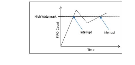
Shown below is an example of interrupts generated for the High Watermark. As shown, the interrupt is generated as the FIFO Word Count crosses the High Watermark. The interrupt will not be generated a second time until the count goes below the watermark and then above it again.
FUNCTION REGISTER MAP
Key:
Bold Italic = Input
Bold Underline = Output
*When an event is detected, the bit associated with the event is set in this register and will remain set until the user clears the event bit. Clearing the bit requires writing a 1 back to the specific bit that was set when read (i.e., write-1-to-clear, writing a “1” to a bit set to “1” will set the bit to “0).
Receive Registers
| 0x1004 | Receive FIFO Buffer Data Ch 1 | R |
|---|---|---|
| 0x1084 | Receive FIFO Buffer Data Ch 2 | R |
| 0x1104 | Receive FIFO Buffer Data Ch 3 | R |
| 0x1184 | Receive FIFO Buffer Data Ch 4 | R |
| 0x1204 | Receive FIFO Buffer Data Ch 5 | R |
| 0x1284 | Receive FIFO Buffer Data Ch 6 | R |
| 0x1304 | Receive FIFO Buffer Data Ch 7 | R |
| 0x1384 | Receive FIFO Buffer Data Ch 8 | R |
| 0x1008 | Receive FIFO Word Count Ch 1 | R |
|---|---|---|
| 0x1088 | Receive FIFO Word Count Ch 2 | R |
| 0x1108 | Receive FIFO Word Count Ch 3 | R |
| 0x1188 | Receive FIFO Word Count Ch 4 | R |
| 0x1208 | Receive FIFO Word Count Ch 5 | R |
| 0x1288 | Receive FIFO Word Count Ch 6 | R |
| 0x1308 | Receive FIFO Word Count Ch 7 | R |
| 0x1388 | Receive FIFO Word Count Ch 8 | R |
| 0x100C | Receive FIFO Frame Count Ch 1 | R |
|---|---|---|
| 0x108C | Receive FIFO Frame Count Ch 2 | R |
| 0x110C | Receive FIFO Frame Count Ch 3 | R |
| 0x118C | Receive FIFO Frame Count Ch 4 | R |
| 0x120C | Receive FIFO Frame Count Ch 5 | R |
| 0x128C | Receive FIFO Frame Count Ch 6 | R |
| 0x130C | Receive FIFO Frame Count Ch 7 | R |
| 0x138C | Receive FIFO Frame Count Ch 8 | R |
Receive FIFO Threshold Registers
| 0x1040 | Rx Buffer Almost Full Ch 1 | R/W |
|---|---|---|
| 0x10C0 | Rx Buffer Almost Full Ch 2 | R/W |
| 0x1140 | Rx Buffer Almost Full Ch 3 | R/W |
| 0x11C0 | Rx Buffer Almost Full Ch 4 | R/W |
| 0x1240 | Rx Buffer Almost Full Ch 5 | R/W |
| 0x12C0 | Rx Buffer Almost Full Ch 6 | R/W |
| 0x1340 | Rx Buffer Almost Full Ch 7 | R/W |
| 0x13C0 | Rx Buffer Almost Full Ch 8 | R/W |
| 0x1044 | Rx Buffer High Watermark Ch 1 | R/W |
|---|---|---|
| 0x10C4 | Rx Buffer High Watermark Ch 2 | R/W |
| 0x1144 | Rx Buffer High Watermark Ch 3 | R/W |
| 0x11C4 | Rx Buffer High Watermark Ch 4 | R/W |
| 0x1244 | Rx Buffer High Watermark Ch 5 | R/W |
| 0x12C4 | Rx Buffer High Watermark Ch 6 | R/W |
| 0x1344 | Rx Buffer High Watermark Ch 7 | R/W |
| 0x13C4 | Rx Buffer High Watermark Ch 8 | R/W |
| 0x1048 | Rx Buffer Low Watermark Ch 1 | R/W |
|---|---|---|
| 0x10C8 | Rx Buffer Low Watermark Ch 2 | R/W |
| 0x1148 | Rx Buffer Low Watermark Ch 3 | R/W |
| 0x11C8 | Rx Buffer Low Watermark Ch 4 | R/W |
| 0x1248 | Rx Buffer Low Watermark Ch 5 | R/W |
| 0x12C8 | Rx Buffer Low Watermark Ch 6 | R/W |
| 0x1348 | Rx Buffer Low Watermark Ch 7 | R/W |
| 0x13C8 | Rx Buffer Low Watermark Ch 8 | R/W |
Transmit Registers
| 0x1010 | Transmit FIFO Buffer Data Ch 1 | W |
|---|---|---|
| 0x1090 | Transmit FIFO Buffer Data Ch 2 | W |
| 0x1110 | Transmit FIFO Buffer Data Ch 3 | W |
| 0x1190 | Transmit FIFO Buffer Data Ch 4 | W |
| 0x1210 | Transmit FIFO Buffer Data Ch 5 | W |
| 0x1290 | Transmit FIFO Buffer Data Ch 6 | W |
| 0x1310 | Transmit FIFO Buffer Data Ch 7 | W |
| 0x1390 | Transmit FIFO Buffer Data Ch 8 | W |
| 0x1014 | Transmit FIFO Word Count Ch 1 | R |
|---|---|---|
| 0x1094 | Transmit FIFO Word Count Ch 2 | R |
| 0x1114 | Transmit FIFO Word Count Ch 3 | R |
| 0x1194 | Transmit FIFO Word Count Ch 4 | R |
| 0x1214 | Transmit FIFO Word Count Ch 5 | R |
| 0x1294 | Transmit FIFO Word Count Ch 6 | R |
| 0x1314 | Transmit FIFO Word Count Ch 7 | R |
| 0x1394 | Transmit FIFO Word Count Ch 8 | R |
| 0x1018 | Transmit FIFO Frame Count Ch 1 | R |
|---|---|---|
| 0x1098 | Transmit FIFO Frame Count Ch 2 | R |
| 0x1118 | Transmit FIFO Frame Count Ch 3 | R |
| 0x1198 | Transmit FIFO Frame Count Ch 4 | R |
| 0x1218 | Transmit FIFO Frame Count Ch 5 | R |
| 0x1298 | Transmit FIFO Frame Count Ch 6 | R |
| 0x1318 | Transmit FIFO Frame Count Ch 7 | R |
| 0x1398 | Transmit FIFO Frame Count Ch 8 | R |
Transmit FIFO Threshold Registers
| 0x103C | Transmit FIFO Buffer Almost Empty Ch 1 | R/W |
|---|---|---|
| 0x10BC | Transmit FIFO Buffer Almost Empty Ch 2 | R/W |
| 0x113C | Transmit FIFO Buffer Almost Empty Ch 3 | R/W |
| 0x11BC | Transmit FIFO Buffer Almost Empty Ch 4 | R/W |
| 0x123C | Transmit FIFO Buffer Almost Empty Ch 5 | R/W |
| 0x12BC | Transmit FIFO Buffer Almost Empty Ch 6 | R/W |
| 0x133C | Transmit FIFO Buffer Almost Empty Ch 7 | R/W |
| 0x13BC | Transmit FIFO Buffer Almost Empty Ch 8 | R/W |
Control Registers
| 0x102C | Baud/Bit Timing Ch 1 | R/W |
|---|---|---|
| 0x10AC | Baud/Bit Timing Ch 2 | R/W |
| 0x112C | Baud/Bit Timing Ch 3 | R/W |
| 0x11AC | Baud/Bit Timing Ch 4 | R/W |
| 0x122C | Baud/Bit Timing Ch 5 | R/W |
| 0x12AC | Baud/Bit Timing Ch 6 | R/W |
| 0x132C | Baud/Bit Timing Ch 7 | R/W |
| 0x13AC | Baud/Bit Timing Ch 8 | R/W |
| 0x1000 | Control Ch 1 | R/W |
|---|---|---|
| 0x1080 | Control Ch 2 | R/W |
| 0x1100 | Control Ch 3 | R/W |
| 0x1180 | Control Ch 4 | R/W |
| 0x1200 | Control Ch 5 | R/W |
| 0x1280 | Control Ch 6 | R/W |
| 0x1300 | Control Ch 7 | R/W |
| 0x1380 | Control Ch 8 | R/W |
| 0x1060 | Source Address (J1939 only) Ch 1 | R/W |
|---|---|---|
| 0x10E0 | Source Address (J1939 only) Ch 2 | R/W |
| 0x1160 | Source Address (J1939 only) Ch 3 | R/W |
| 0x11E0 | Source Address (J1939 only) Ch 4 | R/W |
| 0x1260 | Source Address (J1939 only) Ch 5 | R/W |
| 0x12E0 | Source Address (J1939 only) Ch 6 | R/W |
| 0x1360 | Source Address (J1939 only) Ch 7 | R/W |
| 0x13E0 | Source Address (J1939 only) Ch 8 | R/W |
| 0x1064 | Protocol Assignment (CB3 Only) Ch 1 | R/W |
|---|---|---|
| 0x10E4 | Protocol Assignment (CB3 Only) Ch 2 | R/W |
| 0x1164 | Protocol Assignment (CB3 Only) Ch 3 | R/W |
| 0x11E4 | Protocol Assignment (CB3 Only) Ch 4 | R/W |
| 0x1264 | Protocol Assignment (CB3 Only) Ch 5 | R/W |
| 0x12E4 | Protocol Assignment (CB3 Only) Ch 6 | R/W |
| 0x1364 | Protocol Assignment (CB3 Only) Ch 7 | R/W |
| 0x13E4 | Protocol Assignment (CB3 Only) Ch 8 | R/W |
| 0x1068 | Transmit/Receive Enable State Ch 1 | R/W |
|---|---|---|
| 0x10E8 | Transmit/Receive Enable State Ch 2 | R/W |
| 0x1168 | Transmit/Receive Enable State Ch 3 | R/W |
| 0x11E8 | Transmit/Receive Enable State Ch 4 | R/W |
| 0x1268 | Transmit/Receive Enable State Ch 5 | R/W |
| 0x12E8 | Transmit/Receive Enable State Ch 6 | R/W |
| 0x1368 | Transmit/Receive Enable State Ch 7 | R/W |
| 0x13E8 | Transmit/Receive Enable State Ch 8 | R/W |
Message Status/Monitor Registers
| 0x104C | FIFO Status Ch 1 | R |
|---|---|---|
| 0x10CC | FIFO Status Ch 2 | R |
| 0x114C | FIFO Status Ch 3 | R |
| 0x11CC | FIFO Status Ch 4 | R |
| 0x124C | FIFO Status Ch 5 | R |
| 0x12CC | FIFO Status Ch 6 | R |
| 0x134C | FIFO Status Ch 7 | R |
| 0x13CC | FIFO Status Ch 8 | R |
| 0x1024 | Last Error Code (LEC) Ch 1 | R |
|---|---|---|
| 0x10A4 | Last Error Code (LEC) Ch 2 | R |
| 0x1124 | Last Error Code (LEC) Ch 3 | R |
| 0x11A4 | Last Error Code (LEC) Ch 4 | R |
| 0x1224 | Last Error Code (LEC) Ch 5 | R |
| 0x12A4 | Last Error Code (LEC) Ch 6 | R |
| 0x1324 | Last Error Code (LEC) Ch 7 | R |
| 0x13A4 | Last Error Code (LEC) Ch 8 | R |
| 0x1054 | Bus Status Ch 1 | R/W |
|---|---|---|
| 0x10D4 | Bus Status Ch 2 | R/W |
| 0x1154 | Bus Status Ch 3 | R/W |
| 0x11D4 | Bus Status Ch 4 | R/W |
| 0x1254 | Bus Status Ch 5 | R/W |
| 0x12D4 | Bus Status Ch 6 | R/W |
| 0x1354 | Bus Status Ch 7 | R/W |
| 0x13D4 | Bus Status Ch 8 | R/W |
| 0x1028 | Comm Status Ch 1 | R |
|---|---|---|
| 0x10A8 | Comm Status Ch 2 | R |
| 0x1128 | Comm Status Ch 3 | R |
| 0x11A8 | Comm Status Ch 4 | R |
| 0x1228 | Comm Status Ch 5 | R |
| 0x12A8 | Comm Status Ch 6 | R |
| 0x1328 | Comm Status Ch 7 | R |
| 0x13A8 | Comm Status Ch 8 | R |
| 0x1058 | Core Status Ch 1 | R |
|---|---|---|
| 0x10D8 | Core Status Ch 2 | R |
| 0x1158 | Core Status Ch 3 | R |
| 0x11D8 | Core Status Ch 4 | R |
| 0x1258 | Core Status Ch 5 | R |
| 0x12D8 | Core Status Ch 6 | R |
| 0x1358 | Core Status Ch 7 | R |
| 0x13D8 | Core Status Ch 8 | R |
| 0x1030 | Transmit/Receive Error Counter Ch 1 | R |
|---|---|---|
| 0x10B0 | Transmit/Receive Error Counter Ch 2 | R |
| 0x1130 | Transmit/Receive Error Counter Ch 3 | R |
| 0x11B0 | Transmit/Receive Error Counter Ch 4 | R |
| 0x1230 | Transmit/Receive Error Counter Ch 5 | R |
| 0x12B0 | Transmit/Receive Error Counter Ch 6 | R |
| 0x1330 | Transmit/Receive Error Counter Ch 7 | R |
| 0x13B0 | Transmit/Receive Error Counter Ch 8 | R |
| 0x1050 | Drop Count Ch 1 | R |
|---|---|---|
| 0x10D0 | Drop Count Ch 2 | R |
| 0x1150 | Drop Count Ch 3 | R |
| 0x11D0 | Drop Count Ch 4 | R |
| 0x1250 | Drop Count Ch 5 | R |
| 0x12D0 | Drop Count Ch 6 | R |
| 0x1350 | Drop Count Ch 7 | R |
| 0x13D0 | Drop Count Ch 8 | R |
CANBus Filtering Registers
| 1400 | Filter Control Ch 1 | R/W |
|---|---|---|
| 1480 | Filter Control Ch 2 | R/W |
| 1500 | Filter Control Ch 3 | R/W |
| 1580 | Filter Control Ch 4 | R/W |
| 1600 | Filter Control Ch 5 | R/W |
| 1680 | Filter Control Ch 6 | R/W |
| 1700 | Filter Control Ch 7 | R/W |
| 1780 | Filter Control Ch 8 | R/W |
Acceptance Mask Registers 1-4
| 1408 | 1 Acceptance Mask Register Ch 1 | R/W |
|---|---|---|
| 1410 | 2 Acceptance Mask Register Ch 1 | R/W |
| 1418 | 3 Acceptance Mask Register Ch 1 | R/W |
| 1420 | 4 Acceptance Mask Register Ch 1 | R/W |
| 1488 | 1 Acceptance Mask Register Ch 2 | R/W |
| 1490 | 2 Acceptance Mask Register Ch 2 | R/W |
| 1498 | 3 Acceptance Mask Register Ch 2 | R/W |
| 14A0 | 4 Acceptance Mask Register Ch 2 | R/W |
| 1508 | 1 Acceptance Mask Register Ch 3 | R/W |
| 1510 | 2 Acceptance Mask Register Ch 3 | R/W |
| 1518 | 3 Acceptance Mask Register Ch 3 | R/W |
| 1520 | 4 Acceptance Mask Register Ch 3 | R/W |
| 1588 | 1 Acceptance Mask Register Ch 4 | R/W |
| 1590 | 2 Acceptance Mask Register Ch 4 | R/W |
| 1598 | 3 Acceptance Mask Register Ch 4 | R/W |
| 15A0 | 4 Acceptance Mask Register Ch 4 | R/W |
| 1608 | 1 Acceptance Mask Register Ch 5 | R/W |
| 1610 | 2 Acceptance Mask Register Ch 5 | R/W |
| 1618 | 3 Acceptance Mask Register Ch 5 | R/W |
| 1620 | 4 Acceptance Mask Register Ch 5 | R/W |
| 1688 | 1 Acceptance Mask Register Ch 6 | R/W |
| 1690 | 2 Acceptance Mask Register Ch 6 | R/W |
| 1698 | 3 Acceptance Mask Register Ch 6 | R/W |
| 16A0 | 4 Acceptance Mask Register Ch 6 | R/W |
| 1708 | 1 Acceptance Mask Register Ch 7 | R/W |
| 1710 | 2 Acceptance Mask Register Ch 7 | R/W |
| 1718 | 3 Acceptance Mask Register Ch 7 | R/W |
| 1720 | 4 Acceptance Mask Register Ch 7 | R/W |
| 1788 | 1 Acceptance Mask Register Ch 8 | R/W |
| 1790 | 2 Acceptance Mask Register Ch 8 | R/W |
| 1798 | 3 Acceptance Mask Register Ch 8 | R/W |
| 17A0 | 4 Acceptance Mask Register Ch 8 | R/W |
| 140C | 1 Acceptance Code Register Ch 1 | R/W |
|---|---|---|
| 1414 | 2 Acceptance Code Register Ch 1 | R/W |
| 141C | 3 Acceptance Code Register Ch 1 | R/W |
| 1424 | 4 Acceptance Code Register Ch 1 | R/W |
| 148C | 1 Acceptance Code Register Ch 2 | R/W |
| 1494 | 2 Acceptance Code Register Ch 2 | R/W |
| 149C | 3 Acceptance Code Register Ch 2 | R/W |
| 14A4 | 4 Acceptance Code Register Ch 2 | R/W |
| 150C | 1 Acceptance Code Register Ch 3 | R/W |
| 1514 | 2 Acceptance Code Register Ch 3 | R/W |
| 151C | 3 Acceptance Code Register Ch 3 | R/W |
| 1524 | 4 Acceptance Code Register Ch 3 | R/W |
| 158C | 1 Acceptance Code Register Ch 4 | R/W |
| 1594 | 2 Acceptance Code Register Ch 4 | R/W |
| 159C | 3 Acceptance Code Register Ch 4 | R/W |
| 15A4 | 4 Acceptance Code Register Ch 4 | R/W |
| 160C | 1 Acceptance Code Register Ch 5 | R/W |
| 1614 | 2 Acceptance Code Register Ch 5 | R/W |
| 161C | 3 Acceptance Code Register Ch 5 | R/W |
| 1624 | 4 Acceptance Code Register Ch 5 | R/W |
| 168C | 1 Acceptance Code Register Ch 6 | R/W |
| 1694 | 2 Acceptance Code Register Ch 6 | R/W |
| 169C | 3 Acceptance Code Register Ch 6 | R/W |
| 16A4 | 4 Acceptance Code Register Ch 6 | R/W |
| 170C | 1 Acceptance Code Register Ch 7 | R/W |
| 1714 | 2 Acceptance Code Register Ch 7 | R/W |
| 171C | 3 Acceptance Code Register Ch 7 | R/W |
| 1724 | 4 Acceptance Code Register Ch 7 | R/W |
| 178C | 1 Acceptance Code Register Ch 8 | R/W |
| 1794 | 2 Acceptance Code Register Ch 8 | R/W |
| 179C | 3 Acceptance Code Register Ch 8 | R/W |
| 17A4 | 4 Acceptance Code Register Ch 8 | R/W |
Module Common Registers
Refer to “Module Common Registers Module Manual” for the Module Common Registers Function Register Map.
Status Registers
Bit
| 0x0800 | BIT Dynamic Status | R |
|---|---|---|
| 0x0804 | BIT Latched Status* | R/W |
| 0x0808 | BIT Interrupt Enable | R/W |
| 0x080C | BIT Set Edge/Level Interrupt | R/W |
Status
| 0x0810 | Dynamic Status | R |
|---|---|---|
| 0x0814 | Latched Status* | R/W |
| 0x0818 | Interrupt Enable | R/W |
| 0x081C | Set Edge/Level Interrupt | R/W |
APPENDIX: PIN-OUT DETAILS
Pin-out details (for reference) are shown below, with respect to DATAIO. Additional information on pin-outs can be found in the Motherboard Operational Manuals
CBx Pin-Out Table
| Module Signal (Ref Only) | 44-Pin I/O | 50-Pin I/O (Mod Slot 1-J3) | 50-Pin I/O (Mod Slot 2-J4) | 50-Pin I/O (Mod Slot 3-J3) | 50-Pin I/O (Mod Slot 3-J4) | CAN 2.0 A/B, J1939, Program. CB1/2 (CB1-3) |
|---|---|---|---|---|---|---|
| DATIO1 | 2 | 10 | 1 | 2 | CANH-CH1 | |
| DATIO2 | 24 | 35 | 26 | 27 | CANL-CH1 | |
| DATIO3 | 3 | 11 | 2 | 3 | CANH-CH2 | |
| DATIO4 | 25 | 36 | 27 | 28 | CANL-CH2 | |
| DATIO5 | 5 | 13 | 4 | 5 | ||
| DATIO6 | 27 | 38 | 29 | 30 | ||
| DATIO7 | 7 | 14 | 5 | 6 | CANH-CH3 | |
| DATIO8 | 29 | 39 | 30 | 31 | CANL-CH3 | |
| DATIO9 | 8 | 15 | 6 | 7 | CANH-CH4 | |
| DATIO10 | 30 | 40 | 31 | 32 | CANL-CH4 | |
| DATIO11 | 10 | 17 | 8 | 9 | ||
| DATIO12 | 32 | 42 | 33 | 34 | ||
| DATIO13 | 12 | 18 | 9 | 17 | CANH-CH5 | |
| DATIO14 | 34 | 43 | 34 | 42 | CANL-CH5 | |
| DATIO15 | 13 | 19 | 10 | 18 | CANH-CH6 | |
| DATIO16 | 35 | 44 | 35 | 43 | CANL-CH6 | |
| DATIO17 | 15 | 44 | 35 | 43 | ||
| DATIO18 | 37 | 46 | 37 | 45 | ||
| DATIO19 | 17 | 22 | 13 | 21 | CANH-CH7 | |
| DATIO20 | 39 | 47 | 38 | 46 | CANL-CH7 | |
| DATIO21 | 18 | 23 | 14 | 22 | CANH-CH8 | |
| DATIO22 | 40 | 48 | 39 | 47 | CANL-CH8 | |
| DATIO23 | 20 | 25 | 16 | 24 | ||
| DATIO24 | 42 | 50 | 41 | 49 | ||
| DATIO25 | 4 | 12 | 3 | 4 | ||
| DATIO26 | 26 | 37 | 28 | 29 | ||
| DATIO27 | 9 | 16 | 7 | 8 | ||
| DATIO28 | 31 | 41 | 32 | 33 | ||
| DATIO29 | 14 | 20 | 11 | 19 | ||
| DATIO30 | 36 | 45 | 36 | 44 | ||
| DATIO31 | 19 | 24 | 15 | 23 | ||
| DATIO32 | 41 | 49 | 40 | 48 | ||
| DATIO33 | 6 | |||||
| DATIO34 | 28 | |||||
| DATIO35 | 11 | |||||
| DATIO36 | 33 | |||||
| DATIO37 | 16 | |||||
| DATIO38 | 38 | |||||
| DATIO39 | 21 | |||||
| DATIO40 | 43 | |||||
| N/A |
STATUS AND INTERRUPTS
Status registers indicate the detection of faults or events. The status registers can be channel bit-mapped or event bit-mapped. An example of a channel bit-mapped register is the BIT status register, and an example of an event bit-mapped register is the FIFO status register.
For those status registers that allow interrupts to be generated upon the detection of the fault or the event, there are four registers associated with each status: Dynamic, Latched, Interrupt Enabled, and Set Edge/Level Interrupt.
Dynamic Status: The Dynamic Status register indicates the current condition of the fault or the event. If the fault or the event is momentary, the contents in this register will be clear when the fault or the event goes away. The Dynamic Status register can be polled, however, if the fault or the event is sporadic, it is possible for the indication of the fault or the event to be missed.
Latched Status: The Latched Status register indicates whether the fault or the event has occurred and keeps the state until it is cleared by the user. Reading the Latched Status register is a better alternative to polling the Dynamic Status register because the contents of this register will not clear until the user commands to clear the specific bit(s) associated with the fault or the event in the Latched Status register. Once the status register has been read, the act of writing a 1 back to the applicable status register to any specific bit (channel/event) location will “clear” the bit (set the bit to 0). When clearing the channel/event bits, it is strongly recommended to write back the same bit pattern as read from the Latched Status register. For example, if the channel bit-mapped Latched Status register contains the value 0x0000 0005, which indicates fault/event detection on channel 1 and 3, write the value 0x0000 0005 to the Latched Status register to clear the fault/event status for channel 1 and 3. Writing a “1” to other channels that are not set (example 0x0000 000F) may result in incorrectly “clearing” incoming faults/events for those channels (example, channel 2 and 4).
Interrupt Enable: If interrupts are preferred upon the detection of a fault or an event, enable the specific channel/event interrupt in the Interrupt Enable register. The bits in Interrupt Enable register map to the same bits in the Latched Status register. When a fault or event occurs, an interrupt will be fired. Subsequent interrupts will not trigger until the application acknowledges the fired interrupt by clearing the associated channel/event bit in the Latched Status register. If the interruptible condition is still persistent after clearing the bit, this may retrigger the interrupt depending on the Edge/Level setting.
Set Edge/Level Interrupt: When interrupts are enabled, the condition on retriggering the interrupt after the Latch Register is “cleared” can be specified as “edge” triggered or “level” triggered. Note, the Edge/Level Trigger also affects how the Latched Register value is adjusted after it is “cleared” (see below).
Edge triggered: An interrupt will be retriggered when the Latched Status register change from low (0) to high (1) state. Uses for edge-triggered interrupts would include transition detections (Low-to-High transitions, High-to-Low transitions) or fault detections. After “clearing” an interrupt, another interrupt will not occur until the next transition or the re-occurrence of the fault again.
Level triggered: An interrupt will be generated when the Latched Status register remains at the high (1) state. Level-triggered interrupts are used to indicate that something needs attention.
Interrupt Vector and Steering
When interrupts are enabled, the interrupt vector associated with the specific interrupt can be programmed with a unique number/identifier defined by the user such that it can be utilized in the Interrupt Service Routine (ISR) to identify the type of interrupt. When an interrupt occurs, the contents of the Interrupt Vector registers is reported as part of the interrupt mechanism. In addition to specifying the interrupt vector, the interrupt can be directed (“steered”) to the native bus or to the application running on the onboard ARM processor.
Interrupt Trigger Types
In most applications, limiting the number of interrupts generated is preferred as interrupts are costly, thus choosing the correct Edge/Level interrupt trigger to use is important.
Example 1: Fault detection
This example illustrates interrupt considerations when detecting a fault like an “open” on a line. When an “open” is detected, the system will receive an interrupt. If the “open” on the line is persistent and the trigger is set to “edge”, upon “clearing” the interrupt, the system will not regenerate another interrupt. If, instead, the trigger is set to “level”, upon “clearing” the interrupt, the system will re-generate another interrupt. Thus, in this case, it will be better to set the trigger type to “edge”.
Example 2: Threshold detection
This example illustrates interrupt considerations when detecting an event like reaching or exceeding the “high watermark” threshold value. In a communication device, when the number of elements received in the FIFO reaches the high-watermark threshold, an interrupt will be generated. Normally, the application would read the count of the number of elements in the FIFO and read this number of elements from the FIFO. After reading the FIFO data, the application would “clear” the interrupt. If the trigger type is set to “edge”, another interrupt will be generated only if the number of elements in FIFO goes below the “high watermark” after the “clearing” the interrupt and then fills up to reach the “high watermark” threshold value. Since receiving communication data is inherently asynchronous, it is possible that data can continue to fill the FIFO as the application is pulling data off the FIFO. If, at the time the interrupt is “cleared”, the number of elements in the FIFO is at or above the “high watermark”, no interrupts will be generated. In this case, it will be better to set the trigger type to “level”, as the purpose here is to make sure that the FIFO is serviced when the number of elements exceeds the high watermark threshold value. Thus, upon “clearing” the interrupt, if the number of elements in the FIFO is at or above the “high watermark” threshold value, another interrupt will be generated indicating that the FIFO needs to be serviced.
Dynamic and Latched Status Registers Examples
The examples in this section illustrate the differences in behavior of the Dynamic Status and Latched Status registers as well as the differences in behavior of Edge/Level Trigger when the Latched Status register is cleared.
Figure 1. Example of Module's Channel-Mapped Dynamic and Latched Status States
No Clearing of
Latched StatusClearing of Latched Status
(Edge-Triggered)Clearing of Latched Status
(Level-Triggered)Time Dynamic Status Latched Status Action Latched Status Action Latched T0 0x0 0x0 Read Latched Register 0x0 Read Latched Register 0x0 T1 0x1 0x1 Read Latched Register 0x1 0x1 T1 0x1 0x1 Write 0x1 to Latched Register Write 0x1 to Latched Register T1 0x1 0x1 0x0 0x1 T2 0x0 0x1 Read Latched Register 0x0 Read Latched Register 0x1 T2 0x0 0x1 Read Latched Register 0x0 Write 0x1 to Latched Register T2 0x0 0x1 Read Latched Register 0x0 0x0 T3 0x2 0x3 Read Latched Register 0x2 Read Latched Register 0x2 T3 0x2 0x3 Write 0x2 to Latched Register Write 0x2 to Latched Register T3 0x2 0x3 0x0 0x2 T4 0x2 0x3 Read Latched Register 0x1 Read Latched Register 0x3 T4 0x2 0x3 Write 0x1 to Latched Register Write 0x3 to Latched Register T4 0x2 0x3 0x0 0x2 T5 0xC 0xF Read Latched Register 0xC Read Latched Register 0xE T5 0xC 0xF Write 0xC to Latched Register Write 0xE to Latched Register T5 0xC 0xF 0x0 0xC T6 0xC 0xF Read Latched Register 0x0 Read Latched 0xC T6 0xC 0xF Read Latched Register 0x0 Write 0xC to Latched Register T6 0xC 0xF Read Latched Register 0x0 0xC T7 0x4 0xF Read Latched Register 0x0 Read Latched Register 0xC T7 0x4 0xF Read Latched Register 0x0 Write 0xC to Latched Register T7 0x4 0xF Read Latched Register 0x0 0x4 T8 0x4 0xF Read Latched Register 0x0 Read Latched Register 0x4 Interrupt Examples
The examples in this section illustrate the interrupt behavior with Edge/Level Trigger.
Figure 2. Illustration of Latched Status State for Module with 4-Channels with Interrupt Enabled
Time Latched Status
(Edge-Triggered -
Clear Multi-Channel)Latched Status
(Edge-Triggered -
Clear Single Channel)Latched Status
(Level-Triggered -
Clear Multi-Channel)Action Latched Action Latched Action Latched T1
(Int 1)Interrupt Generated
Read Latched Registers0x1 Interrupt Generated
Read Latched Registers0x1 Interrupt Generated
Read Latched Registers0x1 T1
(Int 1)Write 0x1 to Latched Register Write 0x1 to Latched Register Write 0x1 to Latched Register T1
(Int 1)0x0 0x0 Interrupt re-triggers
Note, interrupt re-triggers after
each clear until T2.0x1 T3
(Int 2)Interrupt Generated
Read Latched Registers0x2 Interrupt Generated
Read Latched Registers0x2 Interrupt Generated
Read Latched Registers0x2 T3
(Int 2)Write 0x2 to Latched Register Write 0x2 to Latched Register Write 0x2 to Latched Register T3
(Int 2)0x0 0x0 Interrupt re-triggers
Note, interrupt re-triggers after
each clear until T7.0x2 T4
(Int 3)Interrupt Generated
Read Latched Registers0x1 Interrupt Generated
Read Latched Registers0x1 Interrupt Generated
Read Latched Registers0x3 T4
(Int 3)Write 0x1 to Latched Register Write 0x1 to Latched Register Write 0x3 to Latched Register T4
(Int 3)0x0 0x0 Interrupt re-triggers
Note, interrupt re-triggers after
each clear and 0x3 is reported
in Latched Register until T5.0x3 T4
(Int 3)0x0 0x0 Interrupt re-triggers
Note, interrupt re-triggers after
each clear until T7.0x2 T6
(Int 4)Interrupt Generated
Read Latched Registers0xC Interrupt Generated
Read Latched Registers0xC Interrupt Generated
Read Latched Registers0xE T6
(Int 4)Write 0xC to Latched Register Write 0x4 to Latched Register Write 0xE to Latched Register T6
(Int 4)0x0 Interrupt re-triggers
Write 0x8 to Latched Register0x8 Interrupt re-triggers
Note, interrupt re-triggers after
each clear and 0xE is
reported in Latched Register until T7.0xE T6
(Int 4)0x0 0x0 Interrupt re-triggers
Note, interrupt re-triggers after
each clear and 0xC is
reported in Latched Register until T8.0xC T6
(Int 4)0x0 0x0 Interrupt re-triggers
Note, interrupt re-triggers after
each clear and 0x4 is
reported in Latched Register always.0x4 REVISION HISTORY
Motherboard Manual - Status and Interrupts Revision History Revision Revision Date Description C 2021-11-30 C08896; Transition manual to docbuilder format - no technical info change. Link to original
DOCS.NAII REVISIONS Revision Date Description 2026-03-02 Formatting updates to document; no technical changes. 2026-05-18 Fixed formatting issues from conversion to new doc site format. 2026-05-19 Fixed minor formatting issue with Interrupt Examples table structure (removed extraneous cell). 2026-07-15 Revised image files for image quality.
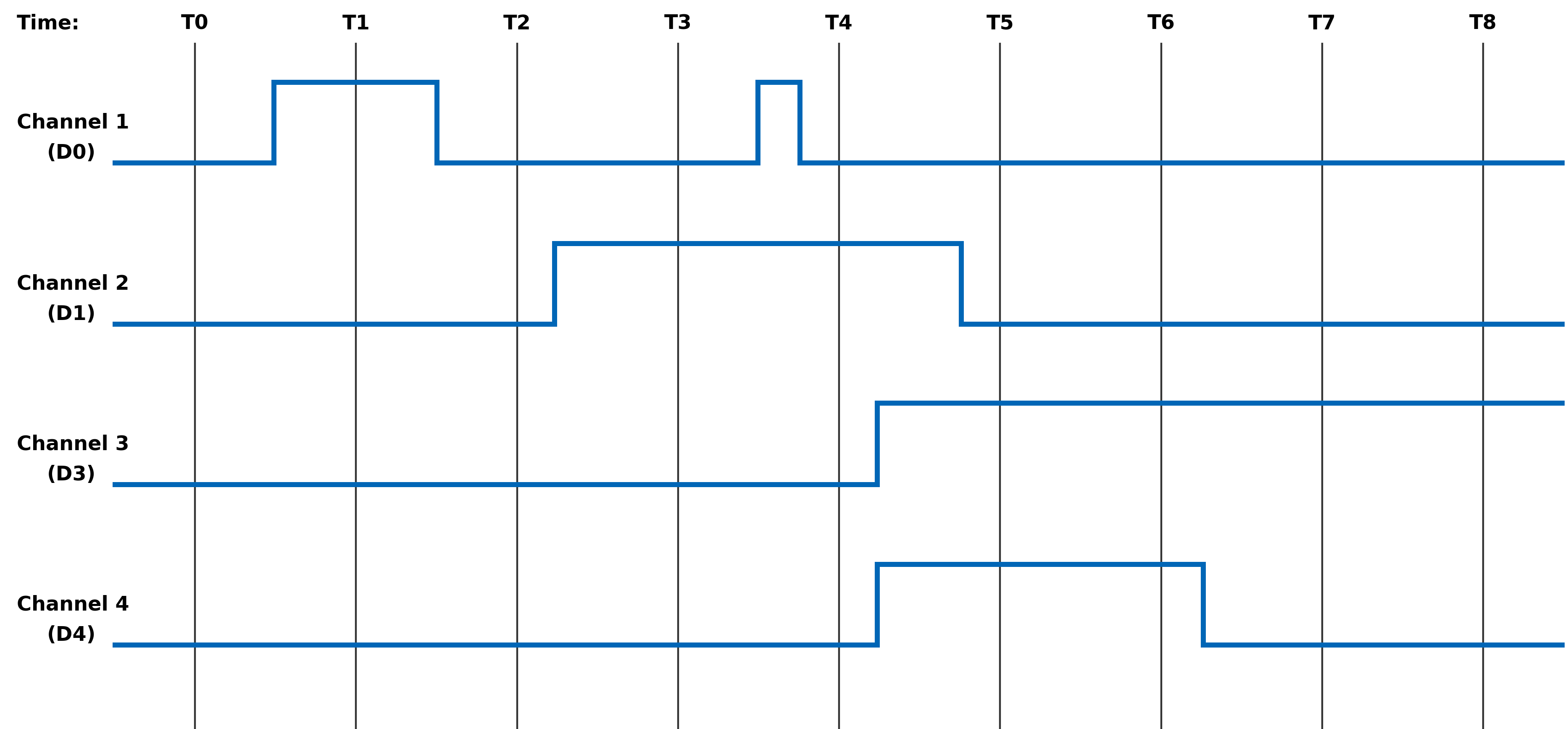
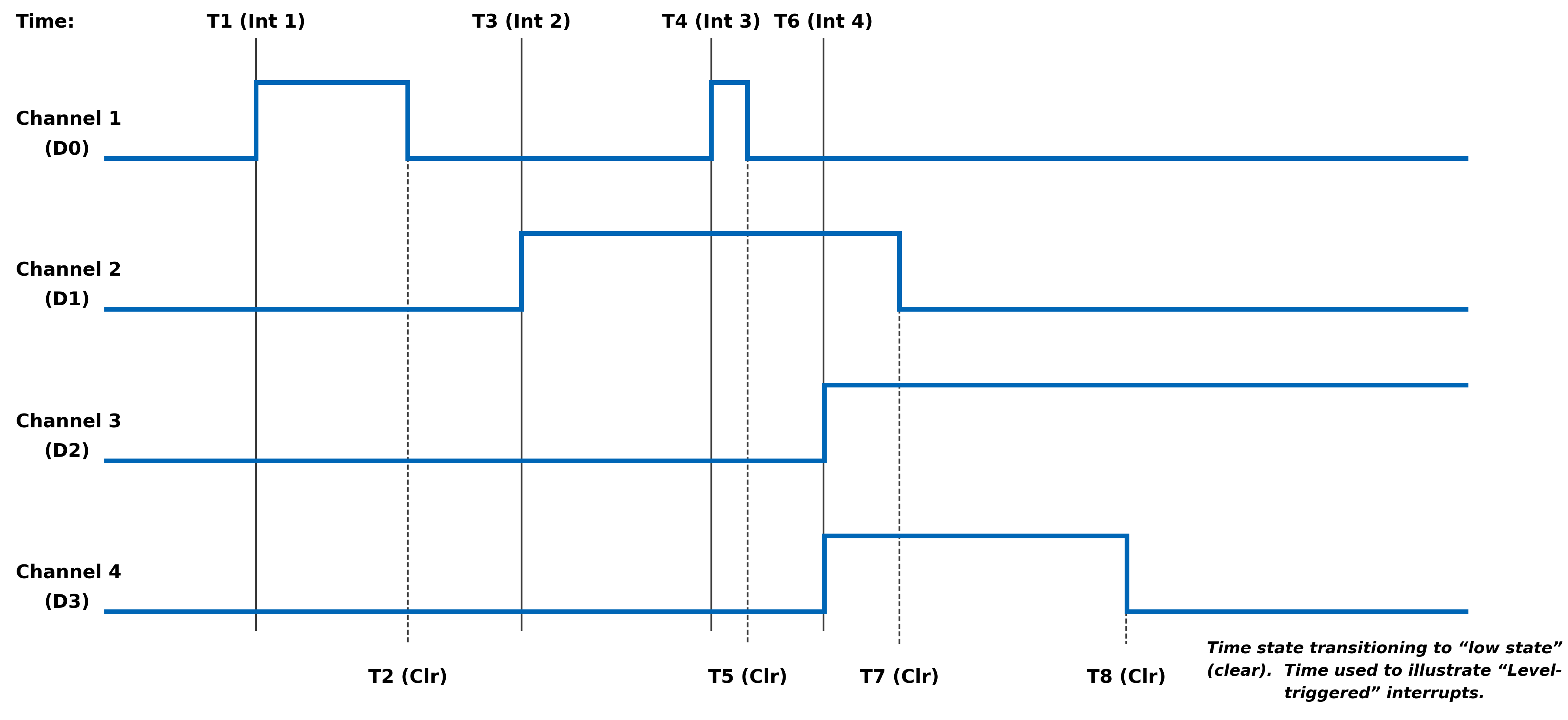
MODULE COMMON REGISTERS
The registers described in this document are common to all NAI Generation 5 modules.
Module Information Registers
The registers in this section provide module information such as firmware revisions, capabilities and unique serial number information.
FPGA Version Registers
The FPGA firmware version registers include registers that contain the Revision, Compile Timestamp, SerDes Revision, Template Revision and Zynq Block Revision information.
FPGA Revision Function: FPGA firmware revision Type: unsigned binary word (32-bit) Data Range: 0x0000 0000 to 0xFFFF FFFF Read/Write: R Initialized Value: Value corresponding to the revision of the board's FPGA Operational Settings: The upper 16-bits are the major revision and the lower 16-bits are the minor revision.
D31 D30 D29 D28 D27 D26 D25 D24 D23 D22 D21 D20 D19 D18 D17 D16 Major Revision Number D15 D14 D13 D12 D11 D10 D9 D8 D7 D6 D5 D4 D3 D2 D1 D0 Minor Revision Number
FPGA Compile Timestamp Function: Compile Timestamp for the FPGA firmware. Type: unsigned binary word (32-bit) Data Range: N/A Read/Write: R Initialized Value: Value corresponding to the compile timestamp of the board's FPGA Operational Settings: The 32-bit value represents the Day, Month, Year, Hour, Minutes and Seconds as formatted in the table:
D31 D30 D29 D28 D27 D26 D25 D24 D23 D22 D21 D20 D19 D18 D17 D16 day (5-bits) month (4-bits) year (6-bits) hr D15 D14 D13 D12 D11 D10 D9 D8 D7 D6 D5 D4 D3 D2 D1 D0 hour (5-bits) minutes (6-bits) seconds (6-bits)
FPGA SerDes Revision Function: FPGA SerDes revision Type: unsigned binary word (32-bit) Data Range: 0x0000 0000 to 0xFFFF FFFF Read/Write: R Initialized Value: Value corresponding to the SerDes revision of the board's FPGA Operational Settings: The upper 16-bits are the major revision, and the lower 16-bits are the minor revision.
D31 D30 D29 D28 D27 D26 D25 D24 D23 D22 D21 D20 D19 D18 D17 D16 Major Revision Number D15 D14 D13 D12 D11 D10 D9 D8 D7 D6 D5 D4 D3 D2 D1 D0 Minor Revision Number
FPGA Template Revision Function: FPGA Template revision Type: unsigned binary word (32-bit) Data Range: 0x0000 0000 to 0xFFFF FFFF Read/Write: R Initialized Value: Value corresponding to the template revision of the board's FPGA Operational Settings: The upper 16-bits are the major revision, and the lower 16-bits are the minor revision.
D31 D30 D29 D28 D27 D26 D25 D24 D23 D22 D21 D20 D19 D18 D17 D16 Major Revision Number D15 D14 D13 D12 D11 D10 D9 D8 D7 D6 D5 D4 D3 D2 D1 D0 Minor Revision Number
FPGA Zynq Block Revision Function: FPGA Zynq Block revision Type: unsigned binary word (32-bit) Data Range: 0x0000 0000 to 0xFFFF FFFF Read/Write: R Initialized Value: Value corresponding to the Zynq block revision of the board's FPGA Operational Settings: The upper 16-bits are the major revision, and the lower 16-bits are the minor revision.
D31 D30 D29 D28 D27 D26 D25 D24 D23 D22 D21 D20 D19 D18 D17 D16 Major Revision Number D15 D14 D13 D12 D11 D10 D9 D8 D7 D6 D5 D4 D3 D2 D1 D0 Minor Revision Number Bare Metal Version Registers
The Bare Metal firmware version registers include registers that contain the Revision and Compile Time information.
Bare Metal Revision Function: Bare Metal firmware revision Type: unsigned binary word (32-bit) Data Range: 0x0000 0000 to 0xFFFF FFFF Read/Write: R Initialized Value: Value corresponding to the revision of the board's Bare Metal Operational Settings: The upper 16-bits are the major revision and the lower 16-bits are the minor revision.
D31 D30 D29 D28 D27 D26 D25 D24 D23 D22 D21 D20 D19 D18 D17 D16 Major Revision Number D15 D14 D13 D12 D11 D10 D9 D8 D7 D6 D5 D4 D3 D2 D1 D0 Minor Revision Number
Bare Metal Compile Time Function: Provides an ASCII representation of the Date/Time for the Bare Metal compile time. Type: 24-character ASCII string - Six (6) unsigned binary word (32-bit) Data Range: N/A Read/Write: R Initialized Value: Value corresponding to the ASCII representation of the compile time of the board's Bare Metal Operational Settings: The six 32-bit words provide an ASCII representation of the Date/Time. The hexadecimal values in the field below represent: May 17 2019 at 15:38:32 Note
little-endian order of ASCII values
Word 1 (Ex. 0x2079614D) D31 D30 D29 D28 D27 D26 D25 D24 D23 D22 D21 D20 D19 D18 D17 D16 Space (0x20) Month ('y' - 0x79) D15 D14 D13 D12 D11 D10 D9 D8 D7 D6 D5 D4 D3 D2 D1 D0 Month ('a' - 0x61) Month ('M' - 0x4D) Word 2 (Ex. 0x32203731) D31 D30 D29 D28 D27 D26 D25 D24 D23 D22 D21 D20 D19 D18 D17 D16 Year ('2' - 0x32) Space (0x20) D15 D14 D13 D12 D11 D10 D9 D8 D7 D6 D5 D4 D3 D2 D1 D0 Day ('7' - 0x37) Day ('1' - 0x31) Word 3 (Ex. 0x20393130) D31 D30 D29 D28 D27 D26 D25 D24 D23 D22 D21 D20 D19 D18 D17 D16 Space (0x20) Year ('9' - 0x39) D15 D14 D13 D12 D11 D10 D9 D8 D7 D6 D5 D4 D3 D2 D1 D0 Year ('1' - 0x31) Year ('0' - 0x30) Word 4 (Ex. 0x31207461) D31 D30 D29 D28 D27 D26 D25 D24 D23 D22 D21 D20 D19 D18 D17 D16 Hour ('1' - 0x31) Space (0x20) D15 D14 D13 D12 D11 D10 D9 D8 D7 D6 D5 D4 D3 D2 D1 D0 'a' (0x74) 't' (0x61) Word 5 (Ex. 0x38333A35) D31 D30 D29 D28 D27 D26 D25 D24 D23 D22 D21 D20 D19 D18 D17 D16 Minute ('8' - 0x38) Minute ('3' - 0x33) D15 D14 D13 D12 D11 D10 D9 D8 D7 D6 D5 D4 D3 D2 D1 D0 ':' (0x3A) Hour ('5' - 0x35) Word 6 (Ex. 0x0032333A) D31 D30 D29 D28 D27 D26 D25 D24 D23 D22 D21 D20 D19 D18 D17 D16 NULL (0x00) Seconds ('2' - 0x32) D15 D14 D13 D12 D11 D10 D9 D8 D7 D6 D5 D4 D3 D2 D1 D0 Seconds ('3' - 0x33) ':' (0x3A) FSBL Version Registers
The FSBL version registers include registers that contain the Revision and Compile Time information for the First Stage Boot Loader (FSBL).
FSBL Revision Function: FSBL firmware revision Type: unsigned binary word (32-bit) Data Range: 0x0000 0000 to 0xFFFF FFFF Read/Write: R Initialized Value: Value corresponding to the revision of the board's FSBL Operational Settings: The upper 16-bits are the major revision, and the lower 16-bits are the minor revision.
D31 D30 D29 D28 D27 D26 D25 D24 D23 D22 D21 D20 D19 D18 D17 D16 Major Revision Number D15 D14 D13 D12 D11 D10 D9 D8 D7 D6 D5 D4 D3 D2 D1 D0 Minor Revision Number
FSBL Compile Time Function: Provides an ASCII representation of the Date/Time for the FSBL compile time. Type: 24-character ASCII string - Six (6) unsigned binary word (32-bit) Data Range: N/A Read/Write: R Initialized Value: Value corresponding to the ASCII representation of the Compile Time of the board's FSBL Operational Settings: The six 32-bit words provide an ASCII representation of the Date/Time. The hexadecimal values in the field below represent: May 17 2019 at 15:38:32
Note
little-endian order of ASCII values
Word 1 (Ex. 0x2079614D) D31 D30 D29 D28 D27 D26 D25 D24 D23 D22 D21 D20 D19 D18 D17 D16 Space (0x20) Month ('y' - 0x79) D15 D14 D13 D12 D11 D10 D9 D8 D7 D6 D5 D4 D3 D2 D1 D0 Month ('a' - 0x61) Month ('M' - 0x4D) Word 2 (Ex. 0x32203731) D31 D30 D29 D28 D27 D26 D25 D24 D23 D22 D21 D20 D19 D18 D17 D16 Year ('2' - 0x32) Space (0x20) D15 D14 D13 D12 D11 D10 D9 D8 D7 D6 D5 D4 D3 D2 D1 D0 Day ('7' - 0x37) Day ('1' - 0x31) Word 3 (Ex. 0x20393130) D31 D30 D29 D28 D27 D26 D25 D24 D23 D22 D21 D20 D19 D18 D17 D16 Space (0x20) Year ('9' - 0x39) D15 D14 D13 D12 D11 D10 D9 D8 D7 D6 D5 D4 D3 D2 D1 D0 Year ('1' - 0x31) Year ('0' - 0x30) Word 4 (Ex. 0x31207461) D31 D30 D29 D28 D27 D26 D25 D24 D23 D22 D21 D20 D19 D18 D17 D16 Hour ('1' - 0x31) Space (0x20) D15 D14 D13 D12 D11 D10 D9 D8 D7 D6 D5 D4 D3 D2 D1 D0 'a' (0x74) 't' (0x61) Word 5 (Ex. 0x38333A35) D31 D30 D29 D28 D27 D26 D25 D24 D23 D22 D21 D20 D19 D18 D17 D16 Minute ('8' - 0x38) Minute ('3' - 0x33) D15 D14 D13 D12 D11 D10 D9 D8 D7 D6 D5 D4 D3 D2 D1 D0 ':' (0x3A) Hour ('5' - 0x35) Word 6 (Ex. 0x0032333A) D31 D30 D29 D28 D27 D26 D25 D24 D23 D22 D21 D20 D19 D18 D17 D16 NULL (0x00) Seconds ('2' - 0x32) D15 D14 D13 D12 D11 D10 D9 D8 D7 D6 D5 D4 D3 D2 D1 D0 Seconds ('3' - 0x33) ':' (0x3A) Module Serial Number Registers
The Module Serial Number registers include registers that contain the Serial Numbers for the Interface Board and the Functional Board of the module.
Interface Board Serial Number Function: Unique 128-bit identifier used to identify the interface board. Type: 16-character ASCII string - Four (4) unsigned binary words (32-bit) Data Range: N/A Read/Write: R Initialized Value: Serial number of the interface board Operational Settings: This register is for information purposes only.
Functional Board Serial Number Function: Unique 128-bit identifier used to identify the functional board. Type: 16-character ASCII string - Four (4) unsigned binary words (32-bit) Data Range: N/A Read/Write: R Initialized Value: Serial number of the functional board Operational Settings: This register is for information purposes only.
Module Capability Function: Provides indication for whether or not the module can support the following: SerDes block reads, SerDes FIFO block reads, SerDes packing (combining two 16-bit values into one 32-bit value) and floating point representation. The purpose for block access and packing is to improve the performance of accessing larger amounts of data over the SerDes interface. Type: unsigned binary word (32-bit) Data Range: 0x0000 0000 to 0x0000 0107 Read/Write: R Initialized Value: 0x0000 0107 Operational Settings: A “1” in the bit associated with the capability indicates that it is supported.
D31 D30 D29 D28 D27 D26 D25 D24 D23 D22 D21 D20 D19 D18 D17 D16 0 0 0 0 0 0 0 0 0 0 0 0 0 0 0 0 D15 D14 D13 D12 D11 D10 D9 D8 D7 D6 D5 D4 D3 D2 D1 D0 0 0 0 0 0 0 0 Flt-Pt 0 0 0 0 0 Pack FIFO Blk Blk
Module Memory Map Revision Function: Module Memory Map revision Type: unsigned binary word (32-bit) Data Range: 0x0000 0000 to 0xFFFF FFFF Read/Write: R Initialized Value: Value corresponding to the Module Memory Map Revision Operational Settings: The upper 16-bits are the major revision and the lower 16-bits are the minor revision.
D31 D30 D29 D28 D27 D26 D25 D24 D23 D22 D21 D20 D19 D18 D17 D16 Major Revision Number D15 D14 D13 D12 D11 D10 D9 D8 D7 D6 D5 D4 D3 D2 D1 D0 Minor Revision Number Module Measurement Registers
The registers in this section provide module temperature measurement information.
Temperature Readings Registers
The temperature registers provide the current, maximum (from power-up) and minimum (from power-up) Zynq and PCB temperatures.
Interface Board Current Temperature Function: Measured PCB and Zynq Core temperatures on Interface Board. Type: signed byte (8-bits) for PCB and signed byte (8-bits) for Zynq core temperatures Data Range: 0x0000 0000 to 0x0000 FFFF Read/Write: R Initialized Value: Value corresponding to the measured PCB and Zynq core temperatures based on the table below Operational Settings: The upper 16-bits are not used, and the lower 16-bits are the PCB and Zynq Core Temperatures. For example, if the register contains the value 0x0000 202C, this represents PCB Temperature = 32° Celsius and Zynq Temperature = 44° Celsius.
D31 D30 D29 D28 D27 D26 D25 D24 D23 D22 D21 D20 D19 D18 D17 D16 0 0 0 0 0 0 0 0 0 0 0 0 0 0 0 0 D15 D14 D13 D12 D11 D10 D9 D8 D7 D6 D5 D4 D3 D2 D1 D0 PCB Temperature Zynq Core Temperature
Functional Board Current Temperature Function: Measured PCB temperature on Functional Board. Type: signed byte (8-bits) for PCB Data Range: 0x0000 0000 to 0x0000 00FF Read/Write: R Initialized Value: Value corresponding to the measured PCB on the table below Operational Settings: The upper 24-bits are not used, and the lower 8-bits are the PCB Temperature. For example, if the register contains the value 0x0000 0019, this represents PCB Temperature = 25° Celsius.
D31 D30 D29 D28 D27 D26 D25 D24 D23 D22 D21 D20 D19 D18 D17 D16 0 0 0 0 0 0 0 0 0 0 0 0 0 0 0 0 D15 D14 D13 D12 D11 D10 D9 D8 D7 D6 D5 D4 D3 D2 D1 D0 0 0 0 0 0 0 0 0 PCB Temperature
Interface Board Maximum Temperature Function: Maximum PCB and Zynq Core temperatures on Interface Board since power-on. Type: signed byte (8-bits) for PCB and signed byte (8-bits) for Zynq core temperatures Data Range: 0x0000 0000 to 0x0000 FFFF Read/Write: R Initialized Value: Value corresponding to the maximum measured PCB and Zynq core temperatures since power-on based on the table below Operational Settings: The upper 16-bits are not used, and the lower 16-bits are the maximum PCB and Zynq Core Temperatures. For example, if the register contains the value 0x0000 5569, this represents maximum PCB Temperature = 85° Celsius and maximum Zynq Temperature = 105° Celsius.
D31 D30 D29 D28 D27 D26 D25 D24 D23 D22 D21 D20 D19 D18 D17 D16 0 0 0 0 0 0 0 0 0 0 0 0 0 0 0 0 D15 D14 D13 D12 D11 D10 D9 D8 D7 D6 D5 D4 D3 D2 D1 D0 PCB Temperature Zynq Core Temperature
Interface Board Minimum Temperature Function: Minimum PCB and Zynq Core temperatures on Interface Board since power-on. Type: signed byte (8-bits) for PCB and signed byte (8-bits) for Zynq core temperatures Data Range: 0x0000 0000 to 0x0000 FFFF Read/Write: R Initialized Value: Value corresponding to the minimum measured PCB and Zynq core temperatures since power-on based on the table below Operational Settings: The upper 16-bits are not used, and the lower 16-bits are the minimum PCB and Zynq Core Temperatures. For example, if the register contains the value 0x0000 D8E7, this represents minimum PCB Temperature = -40° Celsius and minimum Zynq Temperature = -25° Celsius.
D31 D30 D29 D28 D27 D26 D25 D24 D23 D22 D21 D20 D19 D18 D17 D16 0 0 0 0 0 0 0 0 0 0 0 0 0 0 0 0 D15 D14 D13 D12 D11 D10 D9 D8 D7 D6 D5 D4 D3 D2 D1 D0 PCB Temperature Zynq Core Temperature
Functional Board Maximum Temperature Function: Maximum PCB temperature on Functional Board since power-on. Type: signed byte (8-bits) for PCB Data Range: 0x0000 0000 to 0x0000 00FF Read/Write: R Initialized Value: Value corresponding to the measured PCB on the table below Operational Settings: The upper 24-bits are not used, and the lower 8-bits are the PCB Temperature. For example, if the register contains the value 0x0000 0055, this represents PCB Temperature = 85° Celsius.
D31 D30 D29 D28 D27 D26 D25 D24 D23 D22 D21 D20 D19 D18 D17 D16 0 0 0 0 0 0 0 0 0 0 0 0 0 0 0 0 D15 D14 D13 D12 D11 D10 D9 D8 D7 D6 D5 D4 D3 D2 D1 D0 0 0 0 0 0 0 0 0 PCB Temperature
Functional Board Minimum Temperature Function: Minimum PCB temperature on Functional Board since power-on. Type: signed byte (8-bits) for PCB Data Range: 0x0000 0000 to 0x0000 00FF Read/Write: R Initialized Value: Value corresponding to the measured PCB on the table below Operational Settings: The upper 24-bits are not used, and the lower 8-bits are the PCB Temperature. For example, if the register contains the value 0x0000 00D8, this represents PCB Temperature = -40° Celsius.
D31 D30 D29 D28 D27 D26 D25 D24 D23 D22 D21 D20 D19 D18 D17 D16 0 0 0 0 0 0 0 0 0 0 0 0 0 0 0 0 D15 D14 D13 D12 D11 D10 D9 D8 D7 D6 D5 D4 D3 D2 D1 D0 0 0 0 0 0 0 0 0 PCB Temperature Higher Precision Temperature Readings Registers
These registers provide higher precision readings of the current Zynq and PCB temperatures.
Higher Precision Zynq Core Temperature Function: Higher precision measured Zynq Core temperature on Interface Board. Type: signed word (16-bits) for integer part and unsigned word (16-bits) for fractional part Data Range: 0x0000 0000 to 0xFFFF FFFF Read/Write: R Initialized Value: Measured Zynq Core temperature on Interface Board Operational Settings: The upper 16-bits represent the signed integer part of the temperature and the lower 16-bits represent the fractional part of the temperature with the resolution of 1/1000 of degree Celsius. For example, if the register contains the value 0x002B 0271, this represents Zynq Core Temperature = 43.625° Celsius, and value 0xFFF6 0177 represents -10.375° Celsius.
D31 D30 D29 D28 D27 D26 D25 D24 D23 D22 D21 D20 D19 D18 D17 D16 Signed Integer Part of Temperature D15 D14 D13 D12 D11 D10 D9 D8 D7 D6 D5 D4 D3 D2 D1 D0 Fractional Part of Temperature
Higher Precision Interface PCB Temperature Function: Higher precision measured Interface PCB temperature. Type: signed word (16-bits) for integer part and unsigned word (16-bits) for fractional part Data Range: 0x0000 0000 to 0xFFFF FFFF Read/Write: R Initialized Value: Measured Interface PCB temperature Operational Settings: The upper 16-bits represent the signed integer part of the temperature and the lower 16-bits represent the fractional part of the temperature with the resolution of 1/1000 of degree Celsius. For example, if the register contains the value 0x0020 007D, this represents Interface PCB Temperature = 32.125° Celsius, and value 0xFFE8 036B represents -24.875° Celsius.
D31 D30 D29 D28 D27 D26 D25 D24 D23 D22 D21 D20 D19 D18 D17 D16 Signed Integer Part of Temperature D15 D14 D13 D12 D11 D10 D9 D8 D7 D6 D5 D4 D3 D2 D1 D0 Fractional Part of Temperature
Higher Precision Functional PCB Temperature Function: Higher precision measured Functional PCB temperature. Type: signed word (16-bits) for integer part and unsigned word (16-bits) for fractional part Data Range: 0x0000 0000 to 0xFFFF FFFF Read/Write: R Initialized Value: Measured Functional PCB temperature Operational Settings: The upper 16-bits represent the signed integer part of the temperature and the lower 16-bits represent the fractional part of the temperature with the resolution of 1/100 of degree Celsius. For example, if the register contains the value 0x0018 004B, this represents Functional PCB Temperature = 24.75° Celsius, and value 0xFFD9 0019 represents -39.25° Celsius.
D31 D30 D29 D28 D27 D26 D25 D24 D23 D22 D21 D20 D19 D18 D17 D16 Signed Integer Part of Temperature D15 D14 D13 D12 D11 D10 D9 D8 D7 D6 D5 D4 D3 D2 D1 D0 Fractional Part of Temperature Module Health Monitoring Registers
The registers in this section provide module temperature measurement information. If the temperature measurements reaches the Lower Critical or Upper Critical conditions, the module will automatically reset itself to prevent damage to the hardware.
Module Sensor Summary Status Function: The corresponding sensor bit is set if the sensor has crossed any of its thresholds. Type: unsigned binary word (32-bits) Data Range: See table below Read/Write: R Initialized Value: 0 Operational Settings: This register provides a summary for module sensors. When the corresponding sensor bit is set, the Sensor Threshold Status register for that sensor will indicate the threshold condition that triggered the event.
Bit(s) Sensor D31:D6 Reserved D5 Functional Board PCB Temperature D4 Interface Board PCB Temperature D3:D0 Reserved Module Sensor Registers
The registers listed in this section apply to each module sensor listed for the Module Sensor Summary Status register. Each individual sensor register provides a group of registers for monitoring module temperatures readings. From these registers, a user can read the current temperature of the sensor in addition to the minimum and maximum temperature readings since power-up. Upper and lower critical/warning temperature thresholds can be set and monitored from these registers. When a programmed temperature threshold is crossed, the Sensor Threshold Status register will set the corresponding bit for that threshold. The figure below shows the functionality of this group of registers when accessing the Interface Board PCB Temperature sensor as an example.
Sensor Threshold Status Function: Reflects which threshold has been crossed Type: unsigned binary word (32-bits) Data Range: See table below Read/Write: R Initialized Value: 0 Operational Settings: The associated bit is set when the sensor reading exceed the corresponding threshold settings.
Bit(s) Description D31:D4 Reserved D3 Exceeded Upper Critical Threshold D2 Exceeded Upper Warning Threshold D1 Exceeded Lower Critical Threshold D0 Exceeded Lower Warning Threshold
Sensor Current Reading Function: Reflects current reading of temperature sensor Type: Single Precision Floating Point Value (IEEE-754) Data Range: Single Precision Floating Point Value (IEEE-754) Read/Write: R Initialized Value: N/A Operational Settings: The register represents current sensor reading as a single precision floating point value. For example, for a temperature sensor, register value 0x41C6 0000 represents temperature = 24.75° Celsius.
Sensor Minimum Reading Function: Reflects minimum value of temperature sensor since power up Type: Single Precision Floating Point Value (IEEE-754) Data Range: Single Precision Floating Point Value (IEEE-754) Read/Write: R Initialized Value: N/A Operational Settings: The register represents minimum sensor value as a single precision floating point value. For example, for a temperature sensor, register value 0x41C6 0000 represents temperature = 24.75° Celsius.
Sensor Maximum Reading Function: Reflects maximum value of temperature sensor since power up Type: Single Precision Floating Point Value (IEEE-754) Data Range: Single Precision Floating Point Value (IEEE-754) Read/Write: R Initialized Value: N/A Operational Settings: The register represents maximum sensor value as a single precision floating point value. For example, for a temperature sensor, register value 0x41C6 0000 represents temperature = 24.75° Celsius.
Sensor Lower Warning Threshold Function: Reflects lower warning threshold of temperature sensor Type: Single Precision Floating Point Value (IEEE-754) Data Range: Single Precision Floating Point Value (IEEE-754) Read/Write: R/W Initialized Value: Default lower warning threshold (value dependent on specific sensor) Operational Settings: The register represents sensor lower warning threshold as a single precision floating point value. For example, for a temperature sensor, register value 0xC220 0000 represents temperature = -40.0° Celsius.
Sensor Lower Critical Threshold Function: Reflects lower critical threshold of temperature sensor Type: Single Precision Floating Point Value (IEEE-754) Data Range: Single Precision Floating Point Value (IEEE-754) Read/Write: R/W Initialized Value: Default lower critical threshold (value dependent on specific sensor) Operational Settings: The register represents sensor lower critical threshold as a single precision floating point value. For example, for a temperature sensor, register value 0xC25C 0000 represents temperature = -55.0° Celsius.
Sensor Upper Warning Threshold Function: Reflects upper warning threshold of temperature sensor Type: Single Precision Floating Point Value (IEEE-754) Data Range: Single Precision Floating Point Value (IEEE-754) Read/Write: R/W Initialized Value: Default upper warning threshold (value dependent on specific sensor) Operational Settings: The register represents sensor upper warning threshold as a single precision floating point value. For example, for a temperature sensor, register value 0x42AA 0000 represents temperature = 85.0° Celsius.
Sensor Upper Critical Threshold Function: Reflects upper critical threshold of temperature sensor Type: Single Precision Floating Point Value (IEEE-754) Data Range: Single Precision Floating Point Value (IEEE-754) Read/Write: R/W Initialized Value: Default upper critical threshold (value dependent on specific sensor) Operational Settings: The register represents sensor upper critical threshold as a single precision floating point value. For example, for a temperature sensor, register value 0x42FA 0000 represents temperature = 125.0° Celsius. FUNCTION REGISTER MAP
KEY
Configuration/Control Measurement/Status/Board Information
MODULE INFORMATION REGISTERS OFFSET REGISTER NAME ACCESS OFFSET REGISTER NAME ACCESS 0x003C FPGA Revision R 0x0074 Bare Metal Revision R 0x0030 FPGA Compile Timestamp R 0x0080 Bare Metal Compile Time (Bit 0-31) R 0x0034 FPGA SerDes Revision R 0x0084 Bare Metal Compile Time (Bit 32-63) R 0x0038 FPGA Template Revision R 0x0088 Bare Metal Compile Time (Bit 64-95) R 0x0040 FPGA Zynq Block Revision R 0x008C Bare Metal Compile Time (Bit 96-127) R 0x0090 Bare Metal Compile Time (Bit 128-159) R 0x0094 Bare Metal Compile Time (Bit 160-191) R 0x007C FSBL Revision R 0x00B0 FSBL Compile Time (Bit 0-31) R 0x00B4 FSBL Compile Time (Bit 32-63) R 0x00B8 FSBL Compile Time (Bit 64-95) R 0x00BC FSBL Compile Time (Bit 96-127) R 0x00C0 FSBL Compile Time (Bit 128-159) R 0x00C4 FSBL Compile Time (Bit 160-191) R 0x0000 Interface Board Serial Number (Bit 0-31) R 0x0010 Functional Board Serial Number (Bit 0-31) R 0x0034 Interface Board Serial Number (Bit 32-63) R 0x0014 Functional Board Serial Number (Bit 32-63) R 0x0008 Interface Board Serial Number (Bit 64-95) R 0x0018 Functional Board Serial Number (Bit 64-95) R 0x000C Interface Board Serial Number (Bit 96-127) R 0x001C Functional Board Serial Number (Bit 96-127) R 0x0070 Module Capability R 0x01FC Module Memory Map Revision R
MODULE MEASUREMENTS REGISTERS OFFSET REGISTER NAME ACCESS OFFSET REGISTER NAME ACCESS 0x0200 Interface Board PCB/Zynq Current Temp R 0x0208 Functional Board PCB Current Temp R 0x0218 Interface Board PCB/Zynq Max Temp R 0x0228 Functional Board PCB Max Temp R 0x0220 Interface Board PCB/Zynq Min Temp R 0x0230 Functional Board PCB Min Temp R 0x02C0 Higher Precision Zynq Core Temperature R 0x02C4 Higher Precision Interface PCB Temperature R 0x02E0 Higher Precision Functional PCB Temperature R
MODULE HEALTH MONITORING REGISTERS OFFSET REGISTER NAME ACCESS OFFSET REGISTER NAME ACCESS 0x07F8 Module Sensor Summary Status R
REVISION HISTORY
Motherboard Manual - Module Common Registers Revision History Revision Revision Date Description C 2023-08-11 ECO C10649, initial release of module common registers manual. C1 2024-05-15 ECO C11522, removed Zynq Core/Aux/DDR Voltage register descriptions from Module Measurement Registers. Pg.16, updated Module Sensor Summary Status register to add PS references; updated Bit Table to change voltage/current bits to 'reserved'. Pg.16, updated Module/Power Supply Sensor Registers description to better describe register functionality and to add figure. Pg.17, added 'Exceeded' to threshold bit descriptions. Pg.17-18, removed voltage/current references from sensor descriptions. Pg.20, removed Zynq Core/Aux/DDR Voltage register offsets from Module Measurement Registers. Pg.20, updated Module Health Monitoring Registers offset tables. C2 2024-07-10 ECO C11701, pg.16, updated Module Sensor Summary Status register to remove PS references;updated Bit Table to change PS temperature bits to 'reserved'. Pg.16, updated Module SensorRegisters description to remove PS references. Pg.20, updated Module Health MonitoringRegisters offset tables to remove PS temperature register offsets. Link to original
DOCS.NAII REVISIONS Revision Date Description 2025-11-05 Corrected register offsets for Interface Board Min Temp and Function Board Min & Max Temps. 2026-03-02 Formatting updates to document; no technical changes. 2026-05-20 Minor formatting fixes (non-technical changes). 2026-07-15 Updated images for online quality; minor additional formatting updates (no technical changes).


Revision History
Module Manual - CB13x Revision History
|Revision| |Revision Date| |Description| |C| |24-01-2024| |ECO C09979, transition to docbuilder format. Replaced ‘Specifications’ with ‘Data Sheet’. Pg.5, updated CB2 data rate spec; updated Data Length spec. Pg.8, added BIT status verbiage to BIT/Diagnostic Capability. Reorganized ‘Register Descriptions’ by register group. Pg.9, updated Receive FIFO Frame Count ops settings. Pg.10, updated Receive FIFO Buffer High/Low Watermark data range. Pg.10, updated Transmit FIFO Frame Count ops settings. Pg.11, updated Transmit FIFO Buffer Almost Empty data range. Pg.14, removed Baud Rate Change from D8 and moved to D9. Pg.15, updated D31 description. Pg.15, updated Source Address ops settings. Pg.26-27, added separate Channel & FIFO Status register descriptions. Reorganized ‘Function Register Map’ by register group. Added Appendix.| |C1| |01-05-2023| |ECO C10346, pg.11, added Prescaler details/bits to Baud/Bit Timing register.| |C2| |08-01-2024| |EC0 C11135, pg.7, updated Introduction; added Overview section. Pg.9/26/32, added module common registers.|
Module Manual - Status and Interrupts Revision History
|Revision| |Revision Date| |Description| |C| |2021-11-30| |C08896; Transition manual to docbuilder format - no technical info change.|
Module Manual - Module Common Registers Revision History
|Revision| |Revision Date| |Description| |C| |2023-08-11| |ECO C10649, initial release of module common registers manual.|
NAI Cares
North Atlantic Industries (NAI) is a leading independent supplier of Embedded I/O Boards, Single Board Computers, Rugged Power Supplies, Embedded Systems and Motion Simulation and Measurement Instruments for the Military, Aerospace and Industrial Industries. We accelerate our clients’ time-to-mission with a unique approach based on a Configurable Open Systems Architecture™ (COSA®) that delivers the best of both worlds: custom solutions from standard COTS components.
We have built a reputation by listening to our customers, understanding their needs, and designing, testing and delivering board and system-level products for their most demanding air, land and sea requirements. If you have any applications or questions regarding the use of our products, please contact us for an expedient solution.
Please visit us at: www.naii.com or select one of the following for immediate assistance:
Documentation
FAQ
Application Notes
http://www.naii.com/applicationnotes
Calibration and Repairs
http://www.naii.com/calibrationrepairs
Call Us
(631) 567-1100
Link to original