As a leading manufacturer of smart function modules, NAI offers over 100 different modules that cover a wide range of I/O, measurement and simulation, communications, Ethernet switch, and SBC functions. Our ARINC 429/575 Communications Module (AR1) is designed to meet data transfer standards and protocols used in aircraft avionics systems. With its adherence to industry-standard protocols and the ability to support both ARINC 429 and 575 communications, the AR1 offers exceptional performance and reliability. This user manual is designed to help you get the most out of your AR1 function module.
For a brief description of the modules and complete list of specifications, click here for the AR1 data sheet.
AR1 Overview
The AR1 ARINC 429/575 Communications Module offers a variety of features that highlight its role as in data management and as an interface.
Some of the key features include:
ARINC communications: The module supports the following ARINC communications:
ARINC 429: ARINC 429 is a widely adopted data transfer standard, serving as an alternative to MIL-STD-1553. It utilizes a self-clocking, self-synchronizing data bus protocol with separate transmit and receive ports. The physical connection consists of twisted pairs carrying balanced differential signaling. Each data word is 32 bits in length, with most messages containing a single data word. Messages are transmitted at either 12.5 or 100 kbps, allowing other system elements to monitor the bus messages. The transmitter continuously transmits 32-bit data words or the NULL state. A single-wire pair can accommodate one transmitter and up to 20 receivers. Notably, the receiver end of the protocol enables self-clocking, eliminating the need for transmitting clocking data.
ARINC 575: In addition to ARINC 429, the AR1 function module also supports ARINC 575, a data transfer protocol specifically used for the Digital Air Data System (DADS) on commercial and transport aircraft. ARINC 575 defines a digital data bus that distributes crucial air-data information to displays, autopilots, and flight control instrumentation.
While there are minor differences between the digital data bus of ARINC 575 and ARINC 429, the most significant distinction lies in the usage of bit 32. In ARINC 429, bit 32 is reserved for parity, whereas ARINC 575 can utilize bit 32 for either parity (when using BNR encoding) or data (when using BCD encoding).
Receive/Transmit Mode Programmability: Each channel of the module can be programmed to operate in either receive or transmit mode according to your specific application needs.
Flexible Operation: The module supports both 100 kHz and 12.5 kHz operation per channel, allowing you to choose the appropriate speed for your communication requirements.
Transmit Capabilities: Enjoy the convenience of a 255 message FIFO or scheduled transmits per channel, allowing you to efficiently manage and control the transmission of messages. Additionally, asynchronous transmits can be performed alongside scheduled transmits.
Receive Capabilities: Benefit from a 255 message FIFO or mailbox buffering per channel, providing ample storage for incoming messages. This ensures reliable reception and efficient handling of data.
Message Validation: The module supports SDI/Label Filtering, enabling you to validate received messages based on specific criteria per channel. This feature enhances the overall data integrity and ensures only relevant information is processed.
Hardware parity: You have the option to enable selectable hardware parity generation/checking, which adds an extra layer of data integrity verification during transmission and reception.
Receive Time Stamping: Gain valuable insights into message reception with the module’s receive time stamping feature. This allows precise timing analysis and synchronization in your communication system.
Continuous Built-In Test (BIT): The AR1 incorporates continuous BIT functionality, providing self-diagnostics and monitoring capabilities to ensure reliable operation and easy troubleshooting.
Loop-Back Test: Verify the integrity of the module by performing loop-back tests. This feature allows you to validate the communication path and confirm proper functionality.
Tri-State Outputs: The module’s outputs support tri-state functionality, allowing you to control the state of the outputs as needed. This enables seamless integration with other system components.
High and Low-Speed Slew Rate Outputs: The module offers both high and low-speed slew rate outputs, providing flexibility in meeting the requirements of various communication interfaces.
Module Factory Defaults
Speed:
12.5 khz
Gap Time:
4 bits
Interrupt Level:
0
Interrupt Vector:
0x00
Transmit Mode:
Immediate FIFO
Receive Mode:
FIFO
Parity (Odd):
Enabled
Receivers:
Disabled
Transmitters:
Disabled
SDI/Label Matching:
Disabled
Number of Words Tx Buffer:
0
Number of Words Rx Buffer:
0
Rx Buffer, Almost Full:
0x80
Tx Buffer, Almost Empty:
0x20
Tx-Rx Configuration High:
0
Tx-Rx Configuration Low:
0
Channel Control High:
0
Channel Control Low:
0
Built-In-Test:
Enabled
PRINCIPLE OF OPERATION
Module AR1 provides up to 12 programmable ARINC-429 channels. Each channel is software selectable for transmit and/or receive, high or low speed, and odd or no parity. Therefore, AR1 can support multiple ARINC 429 and 575 channels simultaneously.
Receive Operation
Serial BRZ data is decoded for logic states: one, zero or null. Once Word Gap is detected (4 null states) the receiver waits for either a zero or one state to start the serial-to-parallel shift function. If a waveform timing fault is detected before the serial/parallel function is complete, operation is terminated and the receiver returns to waiting for Word Gap detection. The serial-to-parallel output data is validated for odd parity, Label and Serial-to-Digital Interface (SDI).
If message validation (filtering) is enabled, the module compares the SDI/Label of incoming ARINC messages to a list of desired SDI/Labels in validation (match) memory and only stores messages with an SDI/Label in the list. The message is stored in the receive FIFO or mailbox, depending if the channel is in FIFO receive mode or mailbox receive mode. In FIFO Receive Mode, received ARINC messages / words are stored with an associated status word and an optional time-stamp value in the channel’s receive FIFO. Additionally, the Rx FIFO can be set for either bounded or circular mode, which determines FIFO behavior when it is full. In bounded mode, newly received ARINC messages are discarded if the FIFO is full whereas in circular mode, new ARINC messages overwrite the oldest messages in the FIFO. In mailbox mode, received ARINC words are stored in mailboxes or records in RAM that are indexed by the SDI/Label of the ARINC word. Each mailbox contains a status word associated with the message, the ARINC message / word, and an optional 32-bit timestamp value. The status word indicates parity error and new message status.
Transmit Operation
Transmitters are tri-stated when TX is not enabled. Transmit operates in one of three modes: Immediate FIFO, Triggered FIFO, and Scheduled. In immediate mode, ARINC data is sent as soon as data is written to the transmit FIFO. In Triggered FIFO mode, a write to the Transmit Trigger register is needed to start transmission of the transmit FIFO contents. Transmission continues until the FIFO is empty. To transmit more data after the FIFO empties out, issue a new trigger after filling the transmit FIFO with new data.
For either FIFO mode, a transmit FIFO Rate register is provided to control rate of transmission. The contents of this register specify the gap time between transmitted words from the FIFO. The default is the minimum ARINC gap time of 4-bit times.
Schedule mode transmits ARINC data words according to a prebuilt schedule table in Transmit Schedule RAM. In the Schedule table, various commands define what messages are sent and the duration of gaps between each message. Note that a Gap (Gap or Fixed Gap) command must be explicitly added in between each Message command otherwise a gap will not be inserted between messages. The ARINC data words and gap times are stored in the Transmit Message RAM and can be updated on the fly as the schedule executes. A write to the Transmit Trigger register initiates the schedule and commands are executed starting from the first command (address 0x0) in the Schedule RAM. While a schedule is running, an ARINC word can be transmitted asynchronously by writing the async data word to the Async Transmit Data register. After it has transmitted, the Async Data Available bit will be cleared from the Channel Status register and the Async Data Sent Interrupt will be set if enabled.
The Async Data Available bit in Channel Status also gets cleared by a Stop Cmd in a schedule or if a Transmit Stop command is issued from the Transmit Stop register. Use the Fixed Gap command instead of the Gap command to disable async transmissions during the schedule gap time. Gap and Fixed Gap commands can both be used when building the transmit schedule.
Schedule Transmit Commands
ARINC 429/575 scheduling is controlled by commands that are written to the Transmit Schedule RAM. The available commands are:
Schedule Transmit Commands
Command Name
Description
Message
This command takes a parameter that specifies the location in Transmit Message memory containing the ARINC data word to be sent. The word is transmitted when the Message command is executed. This ARINC word can be modified in Tx Message memory while the schedule is running.
Gap
This command takes a parameter that specifies the location in Transmit Message memory containing a 20-bit gap time value. Values less than 4 are invalid. If the previous command was a Message, then that message is transmitted and then the transmitter waits out the specified gap time transmitting nulls. An exception to this is if there is an async data word available. If the gap time is greater or equal to 40 bit times (4-bit gap time plus one ARINC word plus another 4-bit gap time) an async data word, if available, will be transmitted during this time. If a new async data word is made available and the remaining gap time is large enough to accommodate another async data word transmission, then the new async data word will be transmitted after a 4-bit gap time. Multiple async data word transmissions can thus occur as long as the remaining gap time is large enough to accommodate a message and the required minimum 4-bit gap time. Otherwise, the transmitter waits out the remaining gap time before executing the next command.
Fixed Gap
This command takes a parameter that specifies the location in Transmit Message memory containing a 20-bit gap time value. Values less than 4 are invalid. If the previous command was a Message, then that message is transmitted with the specified gap time appended. If the previous command was not a Message, then the transmitter waits for the specified gap time before executing the next command. The difference between the Fixed Gap and Gap command is that Fixed Gap will prevent the transmission of async data words during the gap time. Use Fixed Gap to only allow nulls to be transmitted during the gap time.
Pause
This command causes the transmitter to pause execution of the schedule after transmitting the current word. Either a Transmit Trigger command is issued to resume execution, or a Transmit Stop command is issued to halt execution.
Interrupt
This command causes the Schedule Interrupt to be set if Schedule Interrupt is enabled. An unlatched version of this flag is also visible in the channel status register.
Jump
Jumps to the 9-bit address in Schedule memory pointed to by this command and resumes execution there.
Stop
This command causes the transmitter to stop execution of the schedule after transmitting the current word.
ARINC 429/575 Built-In Test
The AR1 module supports three types of built-in tests: Power-On, Continuous Background and Initiated. The results of these tests are logically ORed together and stored in the BIT Dynamic Status and BIT Latched Status registers.
Power-On Self-Test (POST)/Power-On BIT (PBIT)/Start-Up BIT (SBIT)
The power-on self-test is performed on each channel automatically when power is applied and reports the results in the BIT Status register when complete. After power-on, the Power-on BIT Complete register should be checked to ensure that POST/PBIT/SBIT test is complete before reading the BIT Dynamic Status and BIT Latched Status registers.
Continuous Background Built-In Test (CBIT)
The background Built-In-Test or Continuous BIT (CBIT) runs in the background for each enabled channel. In Transmit operations, internal transmit data is compared to loop-back data received by the ARINC receivers. When the channel is configured for Receive operation, receive data is continuously monitored via a secondary parallel path circuit and compared to the primary input receive data. If the data does not match, the technique used by the automatic background BIT test consists of an “add-2, subtract-1” counting scheme. The BIT counter is incremented by 2 when a BIT-fault is detected and decremented by 1 when there is no BIT fault detected and the BIT counter is greater than 0. When the BIT counter exceeds the (programmed) Background BIT Threshold value, the specific channel’s fault bit in the BIT status register will be set. The “add- 2, subtract-1” counting scheme effectively filters momentary or intermittent anomalies by allowing them to “come and go“ before a BIT fault status or indication is flagged (e.g. BIT faults would register when sustained). This prevents spurious faults from registering valid such as those caused by EMI and/or dirty power causing false BIT faults. Putting more “weight” on errors (“add-2”) and less “weight” on subsequent passing results (subtract-1) will result in a BIT failure indication even if a channel “oscillates” between a pass and fail state. Results of the Continuous BIT are stored in the BIT Dynamic Status and BIT Latched Status register.
Initiated Built-In Test (IBIT)
The Initiated Built-In-Test (IBIT) is an internal loopback available for each channel of the AR1 module. The test is initiated by setting the bit for the associated channel in the Test Enabled register to a 1. Once enabled, they must wait at least 3 msec before checking to see if the bit for the associated channel in the Test Enabled register reads a 0. When the AR1 clears the bit, it means that the test has completed, and its results can be checked. The results of the IBIT is stored in the BIT Dynamic Status and BIT Latched Status registers, a 0 indicates that the channel has passed and a 1 indicates that it failed.
Loop-Back Operation
Transmit and receive operation of an AR1 channel can be verified internally by enabling both Tx and Rx on the same channel. Tx Scheduling is not supported when the channel is placed in this mode.
Transient Protection
The module is normally configured for transient protection but can be specified without if protection is implemented externally.
Status and Interrupts
The AR1 Module provide registers that indicate faults or events. Refer to “Status and Interrupts Module Manual” for the Principle of Operation description.
Module Common Registers
The AR1 Module includes module common registers that provide access to module-level bare metal/FPGA revisions & compile times, unique serial number information, and temperature/voltage/current monitoring. Refer to “Module Common Registers Module Manual” for the detailed information.
REGISTER DESCRIPTIONS
The register descriptions provide the register name, Type, Data Range, Read or Write information, Initialized Value, a description of the function and, in most cases, a data table.
Receive Registers
The registers listed are associated with data that is received on the AR1 channels. Two modes of message storage are supported: Receive FIFO and Receive Mailbox.
Receive FIFO Mode Registers
The Receive FIFO Mode Registers contain information about ARINC messages that are received via the Receive FIFO buffer on the AR1 channel. The registers associated with this feature are:
Receive FIFO Message Buffer
Receive FIFO Message Count
Receive FIFO Almost Full Threshold
Receive FIFO Size
Receive FIFO Message Buffer
Function:
In FIFO receive mode, the received ARINC messages are stored in this buffer.
Type:
unsigned binary word (32-bit)
Range:
0 to 0xFFFF FFFF
Read/Write:
R
Initialized Value:
NA
Operational Settings:
Perform two reads from this register to retrieve the Status word and the ARINC data word, respectively. If Time Stamping is enabled, perform one more read to retrieve the timestamp.
Message Status Word
D31
D30
D29
D28
D27
D26
D25
D24
D23
D22
D21
D20
D19
D18
D17
D16
0
0
0
0
0
0
0
0
0
0
0
0
0
0
0
0
D15
D14
D13
D12
D11
D10
D9
D8
D7
D6
D5
D4
D3
D2
D1
D0
0
0
0
0
0
0
0
0
0
0
0
0
0
0
N
PE
Data Word
D31
D30
D29
D28
D27
D26
D25
D24
D23
D22
D21
D20
D19
D18
D17
D16
D
D
D
D
D
D
D
D
D
D
D
D
D
D
D
D
D15
D14
D13
D12
D11
D10
D9
D8
D7
D6
D5
D4
D3
D2
D1
D0
D
D
D
D
D
D
D
D
D
D
D
D
D
D
D
D
*Timestamp Word (if enabled)
D31
D30
D29
D28
D27
D26
D25
D24
D23
D22
D21
D20
D19
D18
D17
D16
D
D
D
D
D
D
D
D
D
D
D
D
D
D
D
D
D15
D14
D13
D12
D11
D10
D9
D8
D7
D6
D5
D4
D3
D2
D1
D0
D
D
D
D
D
D
D
D
D
D
D
D
D
D
D
D
PE = Parity Error
1 - Calculated parity does not match the received parity bit.
N = New message
1 - Message has not been read yet.
Receive FIFO Message Count
Function:
Contains the number of ARINC messages in the receive FIFO in Receive FIFO mode.
Type:
unsigned binary word (32-bit)
Range:
0 to 255
Read/Write:
R
Initialized Value:
0
Operational Settings:
A received message consists of the message status word and the ARINC data word. If time stamping is enabled, a 32-bit timestamp is also included in the message. For example, if this register reads 1, indicating one message is loaded in the receive FIFO, perform two reads from the Receive FIFO Message Buffer register to retrieve the full message (status word and ARINC data word) if time stamping is disabled or perform three reads from the Receive FIFO Message Buffer register to retrieve the full message (status word, ARINC data word and timestamp word) if time stamping is enabled.
D31
D30
D29
D28
D27
D26
D25
D24
D23
D22
D21
D20
D19
D18
D17
D16
0
0
0
0
0
0
0
0
0
0
0
0
0
0
0
0
D15
D14
D13
D12
D11
D10
D9
D8
D7
D6
D5
D4
D3
D2
D1
D0
0
0
0
0
0
0
0
0
D
D
D
D
D
D
D
D
Receive FIFO Almost Full Threshold
Function:
Specifies the level of the receive FIFO buffer, equal or above, at which the Rx FIFO Almost Full Status bit D1 in the Channel Status register, is flagged (High True).
Type:
unsigned binary word (32-bit)
Range:
0 to 255
Read/Write:
R/W
Initialized Value:
128 (0x0080)
Operational Settings:
If the Interrupt Enable register interrupt is enabled, a SYSTEM interrupt will be generated when the receive FIFO level increases and reaches the threshold level. This register does NOT get reset by a channel reset.
D31
D30
D29
D28
D27
D26
D25
D24
D23
D22
D21
D20
D19
D18
D17
D16
0
0
0
0
0
0
0
0
0
0
0
0
0
0
0
0
D15
D14
D13
D12
D11
D10
D9
D8
D7
D6
D5
D4
D3
D2
D1
D0
0
0
0
0
0
0
0
0
D
D
D
D
D
D
D
D
Receive FIFO Size
Function:
Specifies the size of the Rx FIFO buffer. The default size is 255 messages.
Type:
unsigned binary word (32-bit)
Range:
1 to 255
Read/Write:
R/W
Initialized Value:
255 (0xFF)
Operational Settings:
This setting affects the Rx FIFO size when the Rx FIFO is configured in either Rx FIFO Bounded or Circular mode.
D31
D30
D29
D28
D27
D26
D25
D24
D23
D22
D21
D20
D19
D18
D17
D16
0
0
0
0
0
0
0
0
0
0
0
0
0
0
0
0
D15
D14
D13
D12
D11
D10
D9
D8
D7
D6
D5
D4
D3
D2
D1
D0
0
0
0
0
0
0
0
0
D
D
D
D
D
D
D
D
Receive Mailbox Mode Registers
The registers listed are associated with data that is received on the AR1 channels. Two modes of message storage are supported: Receive FIFO
and Receive Mailbox.
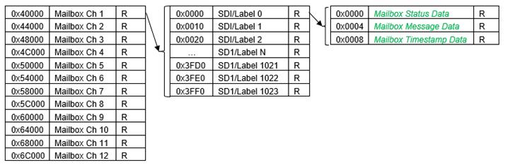
The Receive Mailbox Mode Registers contain information about ARINC messages that are received via mailboxes on the AR1 channel. The registers associated with this feature are:
Receive FIFO SDI/Label Buffer
Receive FIFO SDI/Label Count
Receive FIFO Almost Full Threshold
Receive FIFO Size
Mailbox Status Data
Mailbox Message Data
Mailbox Timestamp Data
Receive FIFO SDI/Label Buffer
Function:
In Mailbox receive mode, SDI/Label of received messages are stored in this buffer.
Type:
unsigned binary word (32-bit)
Range:
0 to 0x0000 03FF
Read/Write:
R
Initialized Value:
N/A
Operational Settings:
In Mailbox receive mode, this FIFO contains the 10-bit SDI/Label of newly received messages. This provides a list to the user showing which mailboxes contain new messages since the last time this FIFO was read.
D31
D30
D29
D28
D27
D26
D25
D24
D23
D22
D21
D20
D19
D18
D17
D16
0
0
0
0
0
0
0
0
0
0
0
0
0
0
0
0
D15
D14
D13
D12
D11
D10
D9
D8
D7
D6
D5
D4
D3
D2
D1
D0
0
0
0
0
0
0
A10
A9
A8
A7
A6
A5
A4
A3
A2
A1
A8-A1
Label (A8 is MSB and A1 is LSB)
A10-A9
SDI
Receive FIFO SDI/Label Count
Function:
Contains the number of newly received SDI/Labels in the receive FIFO in Receive Mailbox mode.
Type:
unsigned binary word (32-bit)
Range:
0 to 255
Read/Write:
R
Initialized Value:
0
Operational Settings:
In Mailbox receive mode, this register contains the number of newly received SDI/Labels in the receive FIFO. The user may perform this number of reads on the Receive FIFO SDI/Label Buffer register to retrieve all SDI/Labels.
D31
D30
D29
D28
D27
D26
D25
D24
D23
D22
D21
D20
D19
D18
D17
D16
0
0
0
0
0
0
0
0
0
0
0
0
0
0
0
0
D15
D14
D13
D12
D11
D10
D9
D8
D7
D6
D5
D4
D3
D2
D1
D0
0
0
0
0
0
0
0
0
D
D
D
D
D
D
D
D
Receive FIFO Almost Full Threshold
Function:
Specifies the level of the receive FIFO buffer, equal or above, at which the Rx FIFO Almost Full Status bit D1 in the Channel Status register, is flagged (High True).
Type:
unsigned binary word (32-bit)
Range:
0 to 255
Read/Write:
R/W
Initialized Value:
128 (0x0080)
Operational Settings:
If the Interrupt Enable register interrupt is enabled, a SYSTEM interrupt will be generated when the receive FIFO level increases and reaches the threshold level. This register does NOT get reset by a channel reset.
D31
D30
D29
D28
D27
D26
D25
D24
D23
D22
D21
D20
D19
D18
D17
D16
0
0
0
0
0
0
0
0
0
0
0
0
0
0
0
0
D15
D14
D13
D12
D11
D10
D9
D8
D7
D6
D5
D4
D3
D2
D1
D0
0
0
0
0
0
0
0
0
D
D
D
D
D
D
D
D
Receive FIFO Size
Function:
Specifies the size of the Rx FIFO buffer. The default size is 255 SDI/Labels.
Type:
unsigned binary word (32-bit)
Range:
1 to 255
Read/Write:
R/W
Initialized Value:
255 (0xFF)
Operational Settings:
This setting affects the Rx FIFO size when the Rx FIFO is configured in either Rx FIFO Bounded or Circular mode.
D31
D30
D29
D28
D27
D26
D25
D24
D23
D22
D21
D20
D19
D18
D17
D16
0
0
0
0
0
0
0
0
0
0
0
0
0
0
0
0
D15
D14
D13
D12
D11
D10
D9
D8
D7
D6
D5
D4
D3
D2
D1
D0
0
0
0
0
0
0
0
0
D
D
D
D
D
D
D
D
Mailbox Status Data
Function:
Stores ARINC Status data word.
Type:
unsigned binary word (32-bit)
Range:
0 to 0x0000 0003
Read/Write:
R
Initialized Value:
0
Operational Settings:
This is a 32-bit value that contains status information associated with the received ARINC word. D1 of 1 indicates that the received ARINC word is a new message. D0 of 1 indicates a parity error is present in the ARINC message. There are 1024 Mailbox Status Data registers, one for each SDI/Label. The user can determine which Mailbox Status Data registers contain new data based on newly received SDI/Labels in the receive FIFO.
D31
D30
D29
D28
D27
D26
D25
D24
D23
D22
D21
D20
D19
D18
D17
D16
0
0
0
0
0
0
0
0
0
0
0
0
0
0
0
0
D15
D14
D13
D12
D11
D10
D9
D8
D7
D6
D5
D4
D3
D2
D1
D0
0
0
0
0
0
0
0
0
0
0
0
0
0
0
N
PE
PE = Parity Error
1 - Calculated parity does not match the received parity bit.
N = New message
1 - This is a new ARINC message.
Mailbox Message Data
Function:
Stores ARINC Message data word.
Type:
unsigned binary word (32-bit)
Range:
0 to 0xFFFF FFFF
Read/Write:
R
Initialized Value:
0
Operational Settings:
This is the 32-bit ARINC data word. There are 1024 Mailbox Message Data registers, one for each SDI/Label. The user can determine which Mailbox Message Data registers contain new data based on newly received SDI/Labels in the receive FIFO.
Mailbox Timestamp Data
Function:
Stores ARINC Timestamp data word.
Type:
unsigned binary word (32-bit)
Range:
0 to 0xFFFF FFFF
Read/Write:
R
Initialized Value:
0
Operational Settings:
This is the 32-bit timestamp associated with the received ARINC word. There are 1024 Mailbox Timestamp Data registers, one for each SDI/Label. The user can determine which Mailbox Timestamp Data registers contain new data based on newly received SDI/Labels in the receive FIFO.
Timestamp Registers
Timestamp Control
Function:
Determines the resolution of the timestamp counter.
Type:
unsigned binary word (32-bit)
Range:
0 to 0x0000 0007
Read/Write:
R/W
Initialized Value:
0 (1 µsec)
Operational Settings:
The LSB can have one of four time values. Set bit D2 to zero out the timestamp counter.
D31
D30
D29
D28
D27
D26
D25
D24
D23
D22
D21
D20
D19
D18
D17
D16
0
0
0
0
0
0
0
0
0
0
0
0
0
0
0
0
D15
D14
D13
D12
D11
D10
D9
D8
D7
D6
D5
D4
D3
D2
D1
D0
0
0
0
0
0
0
0
0
0
0
0
0
0
Z
D
D
Timestamp Control Register
Bit(s)
Name
Description
D31:D3
Reserved
Set Reserved bits to 0.
D2
Zero Timestamp
Set the bit to zero out the timestamp counter
D1:D0
Resolution (R/W)
The following sets the Resolution: (0:0) 1 µs ` (0:1) 10 µs ` (1:0) 100 µs + (1:1) 1 ms
Timestamp Value
Function:
Reads the current 32-bit timestamp.
Type:
unsigned binary word (32-bit)
Range:
0 to 0xFFFF FFFF
Read/Write:
R
Initialized Value:
NA
Operational Settings:
The time value of each LSB is determined by the resolution set in the Timestamp Control register.
D31
D30
D29
D28
D27
D26
D25
D24
D23
D22
D21
D20
D19
D18
D17
D16
D
D
D
D
D
D
D
D
D
D
D
D
D
D
D
D
D15
D14
D13
D12
D11
D10
D9
D8
D7
D6
D5
D4
D3
D2
D1
D0
D
D
D
D
D
D
D
D
D
D
D
D
D
D
D
D
Message Validation Registers
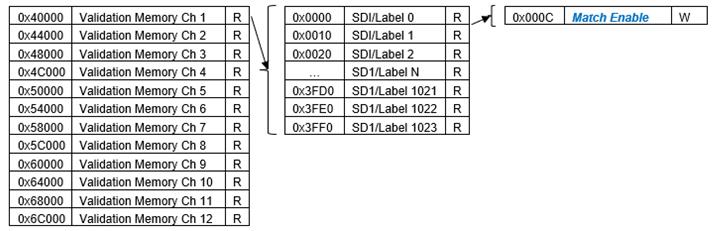
If message validation (filtering) is enabled, the module compares the SDI/Label of incoming ARINC messages to a list of desired SDI/Labels in validation (match) memory and only stores messages with an SDI/Label in the list.
Match Enable
Function:
Enables or disables reception of ARINC words containing the associated SDI/Label.
Type:
unsigned binary word (32-bit)
Range:
0 to 1
Read/Write:
R/W
Initialized Value:
0
Operational Settings:
D0 set to 1 enables reception of ARINC words containing the SDI/Label that is associated with this register. This register only takes effect if the MATCH ENABLE bit is set to 1 in the Channel Control Register. There are 1024 Match Enable Data Registers and each register is indexed by the SDI/Label. Note that bit D1 is a reserved bit and it is fixed to 1.
D31
D30
D29
D28
D27
D26
D25
D24
D23
D22
D21
D20
D19
D18
D17
D16
0
0
0
0
0
0
0
0
0
0
0
0
0
0
0
0
D15
D14
D13
D12
D11
D10
D9
D8
D7
D6
D5
D4
D3
D2
D1
D0
0
0
0
0
0
0
0
0
0
0
0
0
0
0
1
D
Transmit Registers
The registers listed are associated with data that is to be transmitted from the AR1 channels. Two modes of message storage are supported:Transmit FIFO and Transmit Scheduling.
Transmit FIFO Registers
The registers listed are associated with data that is to be transmitted from the AR1 channels. Two modes of message storage are supported: Transmit FIFO and Transmit Scheduling.
The Transmit FIFO Mode Registers contain information about ARINC messages that are to be transmitted via the Transmit FIFO buffer on the AR1 channel. The registers associated with this feature are:
Transmit FIFO Message Buffer
Transmit FIFO Message Count
Transmit FIFO Almost Empty Threshold
Transmit FIFO Rate
Transmit FIFO Message Buffer
Function:
In immediate or triggered FIFO modes, ARINC messages are placed here prior to transmission.
Type:
unsigned binary word (32-bit)
Range:
0 to 0xFFFF FFFF
Read/Write:
W
Initialized Value:
N/A
Operational Settings:
ARINC data words are 32-bits. This memory is shared with the Tx Message memory and is only available in Tx FIFO modes.
Transmit FIFO Message Count
Function:
Contains the number of ARINC 32-bit words in the transmit FIFO.
Type:
unsigned binary word (32-bit)
Range:
0 to 255
Read/Write:
R
Initialized Value:
0
Operational Settings:
Used only in the FIFO transmit modes.
D31
D30
D29
D28
D27
D26
D25
D24
D23
D22
D21
D20
D19
D18
D17
D16
0
0
0
0
0
0
0
0
0
0
0
0
0
0
0
0
D15
D14
D13
D12
D11
D10
D9
D8
D7
D6
D5
D4
D3
D2
D1
D0
0
0
0
0
0
0
0
0
D
D
D
D
D
D
D
D
Transmit FIFO Almost Empty Threshold
Function:
Specifies the level of the transmit buffer, equal or below, at which the Tx FIFO Almost Empty Status bit D5 in the Channel Status register, is flagged (High True).
Type:
unsigned binary word (32-bit)
Range:
0 to 255
Read/Write:
R/W
Initialized Value:
32 decimal (0x0020)
Operational Settings:
If the Interrupt Enable register interrupt is enabled, a SYSTEM interrupt will be generated when the receive FIFO level increases and reaches the threshold level. This register does NOT get reset by a channel reset.
D31
D30
D29
D28
D27
D26
D25
D24
D23
D22
D21
D20
D19
D18
D17
D16
0
0
0
0
0
0
0
0
0
0
0
0
0
0
0
0
D15
D14
D13
D12
D11
D10
D9
D8
D7
D6
D5
D4
D3
D2
D1
D0
0
0
0
0
0
0
0
0
D
D
D
D
D
D
D
D
Transmit FIFO Rate
Function:
Determines the Gap time between transmitted ARINC messages in FIFO transmit modes.
Type:
unsigned binary word (32-bit)
Range:
0-0x000F FFFF
Read/Write:
R/W
Initialized Value:
4
Mode:
FIFO
Operational Settings:
Each LSB is 1 bit time. Rates less than 4 are not valid. This register does NOT get reset by a channel reset.
D31
D30
D29
D28
D27
D26
D25
D24
D23
D22
D21
D20
D19
D18
D17
D16
0
0
0
0
0
0
0
0
0
0
0
0
D
D
D
D
D15
D14
D13
D12
D11
D10
D9
D8
D7
D6
D5
D4
D3
D2
D1
D0
D
D
D
D
D
D
D
D
D
D
D
D
D
D
D
D
Transmit Scheduling Registers
The Transmit Scheduling Registers are utilized when the channel is set up to run a Transmit Schedule. The memories/registers associated with this feature are:
Transmit Schedule RAM
Transmit Message RAM
Async Transmit Data Register
Transmit Schedule RAM Command Format
Function:
The Transmit Schedule RAM consists of 256 32-bit words that are used to set up a self-running transmit schedule. These are the valid command formats for the Transmit Schedule RAM.
Type:
unsigned binary word (32-bit)
Range:
0 to 0x0000 FFFF
Read/Write:
R/W
Initialized Value:
N/A
Operational Settings:
Only bits 0 to 15 are utilized for schedule commands. Bits 12 to 15 specify the command type and bits 0 to 7 or 8 specify the command parameter. Only the Message, Gap, Fixed Gap and Jump commands utilize a command parameter. When the schedule starts, commands are executed sequentially starting from schedule RAM address 0x0.
D31
D30
D29
D28
D27
D26
D25
D24
D23
D22
D21
D20
D19
D18
D17
D16
FUNCTION
0
0
0
0
0
0
0
0
0
0
0
0
0
0
0
0
D15
D14
D13
D12
D11
D10
D9
D8
D7
D6
D5
D4
D3
D2
D1
D0
FUNCTION
0
0
0
0
0
0
0
0
0
0
0
0
0
0
0
0
STOP CMD
0
0
0
1
0
0
0
0
MA7
MA6
MA5
MA4
MA3
MA2
MA1
MA0
MESSAGE CMD1
0
0
1
0
0
0
0
0
MA7
MA6
MA5
MA4
MA3
MA2
MA1
MA0
GAP CMD1
0
0
1
1
0
0
0
0
MA7
MA6
MA5
MA4
MA3
MA2
MA1
MA0
FIXED GAP CMD1
0
1
0
0
0
0
0
0
0
0
0
0
0
0
0
0
PAUSE CMD
0
1
0
1
0
0
0
0
0
0
0
0
0
0
0
0
SCH INTERRUPT CMD
0
1
1
0
0
0
0
SA8
SA7
SA6
SA5
SA4
SA3
SA2
SA1
SA0
JUMP CMD2
0
1
1
1
0
0
0
0
0
0
0
0
0
0
0
0
RESERVED
1
0
0
0
0
0
0
0
0
0
0
0
0
0
0
0
RESERVED
1 MA7-MA0
Address of Tx Message memory organized as 256 x 32.
2 SA8-SA0
Address of next command in Tx Schedule memory organized as 256 x 32.
Transmit Message RAM Data Format
Function:
The Transmit Message RAM consists of 256 32-bit words that are used by the transmit schedule for ARINC message and gap time word storage.
Type:
unsigned binary word (32-bit)
Range:
0 to 0xFFFF FFFF
Read/Write:
R/W
Initialized Value:
N/A
Operational Settings:
Words that are stored in Transmit Message RAM are utilized by Message, Gap and Fixed Gap commands in the Transmit Schedule. In the case of Message commands, the command parameter specifies an address in Transmit Message RAM that contains the 32-bit ARINC message to transmit. In the case of Gap or Fixed Gap commands, the command parameter specifies an address in Transmit Message RAM that contains the gap time value.
Async Transmit Data
Function:
This memory location is the transmit async buffer.
Type:
unsigned binary word (32-bit)
Range:
0 to 0xFFFF FFFF
Read/Write:
R/W
Initialized Value:
0
Operational Settings:
While a schedule is running, a single 32-bit ARINC message that is intended to be transmitted asynchronously must be written to this register. When an async data word is written to this register, the Async Data Available status bit will get set until the async data word is transmitted. If a gap (not fixed gap) time is greater or equal to 40 bit times (4-bit gap time plus one ARINC word plus another 4-bit gap time) the async data word, if available, will be transmitted during this time.
Transmit Control Registers
Control of the transmission of ARINC messages includes the ability to start/resume, pause and stop the transmission of the message.
Transmit Trigger
Function:
Sends a trigger command to the transmitter and is used to start transmission in Triggered FIFO or Scheduled Transmit modes.
Type:
unsigned binary word (32-bit)
Range:
0 to 0x0000 0FFF
Read/Write:
W
Initialized Value:
0
Operational Settings:
Set bit to 1 for the channel to resume transmission after a scheduled pause or Transmit pause command.
D31
D30
D29
D28
D27
D26
D25
D24
D23
D22
D21
D20
D19
D18
D17
D16
0
0
0
0
0
0
0
0
0
0
0
0
0
0
0
0
D15
D14
D13
D12
D11
D10
D9
D8
D7
D6
D5
D4
D3
D2
D1
D0
0
0
0
0
Ch12
Ch11
Ch10
Ch9
Ch8
Ch7
Ch6
Ch5
Ch4
Ch3
Ch2
Ch1
Transmit Pause
Function:
Sends a command to pause the transmitter after the current word and gap time has finished transmitting.
Type:
unsigned binary word (32-bit)
Range:
0 to 0x0000 0FFF
Read/Write:
W
Initialized Value:
0
Modes Affected:
Triggered FIFO and Schedule Transmit
Operational Settings:
Set bit to 1 for the channel to pause transmission in Triggered FIFO or Scheduled Transmit modes. Issue a Transmit Trigger command to resume transmission or issue a Transmit Stop command to halt transmission.
D31
D30
D29
D28
D27
D26
D25
D24
D23
D22
D21
D20
D19
D18
D17
D16
0
0
0
0
0
0
0
0
0
0
0
0
0
0
0
0
D15
D14
D13
D12
D11
D10
D9
D8
D7
D6
D5
D4
D3
D2
D1
D0
0
0
0
0
Ch12
Ch11
Ch10
Ch9
Ch8
Ch7
Ch6
Ch5
Ch4
Ch3
Ch2
Ch1
Transmit Stop
Function:
Sends a command to stop the transmitter after the current word and gap time has been transmitted.
Type:
unsigned binary word (32-bit)
Range:
0 to 0x0000 0FFF
Read/Write:
W
Initialized Value:
0
Modes Affected:
All Transmit modes
Operational Settings:
Set bit to 1 for the channel to stop transmission.
D31
D30
D29
D28
D27
D26
D25
D24
D23
D22
D21
D20
D19
D18
D17
D16
0
0
0
0
0
0
0
0
0
0
0
0
0
0
0
0
D15
D14
D13
D12
D11
D10
D9
D8
D7
D6
D5
D4
D3
D2
D1
D0
0
0
0
0
Ch12
Ch11
Ch10
Ch9
Ch8
Ch7
Ch6
Ch5
Ch4
Ch3
Ch2
Ch1
Control Registers
The AR1 control registers provide the ability to reset all the channels in the AR1 module and configuring and controlling individual AR1 channels.
Channel Control
Function:
Used to configure and control the channels.
Type:
unsigned binary word (32-bit)
Range:
See table
Read/Write:
R/W
Initialized Value:
0
Operational Settings:
When writing to this register, the configuration bits must be maintained when setting the control bits.
Bit(s)
CONTROL FUNCTIONS
Description
D31:D22
RESERVED
Set RESERVED bits to 0.
D21
SCHEDULE INTERRUPT CLEAR
When the SCHEDULE INTERRUPT CLEAR bit is set to 1 by the user, the Schedule Interrupt bit (D10) in the Channel Status register can be cleared.
D20
RESERVED
Set RESERVED bits to 0.
D19
CHANNEL RESET
When the CHANNEL RESET bit is set to 1 by the user, the channel is held in reset until the user sets the bit to 0. The channel reset causes Tx and Rx FIFO buffers to clear out but channel configuration settings remain unchanged.
D18
MATCH MEMORY CLEAR
When the MATCH MEMORY CLEAR bit is set to 1 by the user and if MATCH ENABLE bit is set to 1, all 1024 SDI/Labels will be disabled in Rx Match Memory, which means all received ARINC messages will be filtered out and discarded. This is a self-clearing bit. After setting the bit, allow 100 us to complete.
D17
RECEIVE FIFO CLEAR
When the RECEIVE FIFO CLEAR bit is set to 1 then set to 0 by the user, the Rx FIFO buffer is cleared out and the Rx FIFO count goes to zero.
D16
TRANSMIT FIFO CLEAR
When the TRANSMIT FIFO CLEAR bit is set to 1 then set to 0 by the user, the Tx FIFO buffer is cleared out and the Tx FIFO count goes to zero.
Bit(s)
CONFIGURATION FUNCTIONS
Description/Values
D15:D11
RESERVED
Set RESERVED bits to 0.
D10
STORE ON ERROR DISABLE
If the STORE ON ERROR DISABLE bit is cleared (0) and odd parity is enabled, received words that contain a parity error will be stored in the receive buffer or mailbox. When the STORE ON ERROR DISABLE bit is set (1) and odd parity is enabled, received words that contain a parity error will NOT be stored in the receive buffer or mailbox.
D9
RESERVED
Set RESERVED bit to 0.
D8
TIMESTAMP ENABLE
When TIMESTAMP ENABLE bit is set to 1, the receiver will store a 32-bit time stamp value along with the received ARINC word. There is one time stamp counter per module and it is used across all 12 channels. It has 4 selectable resolutions and can be reset via the Time Stamp Control register. It is recommended to clear the Receive FIFOs whenever the Receive mode or Time Stamp Enable mode is changed to ensure that extraneous data is not leftover from a previous receive operation.
D7
MATCH ENABLE
When the MATCH ENABLE bit is set to 1, the receiver will only store ARINC words which match the SDI/Labels enabled in Rx Match memory.
D6
PARITY DISABLE
The PARITY DISABLE bit when set to 0, causes ARINC bit 32 to be treated as an odd parity bit. The transmitter calculates the ARINC odd parity bit and transmits it as bit 32. The receiver will check the received ARINC word for odd parity and will flag an error if is not. When the PARITY DISABLE bit is set to 1, parity generation and checking will be disabled and both the transmitter and receiver will treat ARINC bit 32 as data and pass it on unchanged.
D5
HIGH SPEED
The HIGH SPEED bit is used to select the data rate. 12.5 kHz = 0 + 100 kHz = 1
D4:D3
TRANSMIT MODE
The TRANSMIT MODE bits are used to select the Transmit Mode. (0:0) = Immediate FIFO mode ` (0:1) = Schedule mode ` (1:0) = Triggered FIFO mode + (1:1) = Invalid mode
D2
TRANSMIT ENABLE
The TRANSMIT ENABLE bit should be set after all transmit parameters have been set up. This is especially important in Immediate FIFO Transmit mode, since this mode will start transmitting as soon as data is put into the Tx FIFO.
D1
RECEIVE MODE
The RECEIVE MODE bit is used to select the storage mode (FIFO or Mailbox) of received messages. FIFO = 0 MBOX = 1
D0
RECEIVER ENABLE
The RECEIVER ENABLE bit should be set after all receive parameters and filters have been set up. After setting this bit, the module will look for a minimum 4-bit gap time before decoding any ARINC bits to prevent it from receiving a partial ARINC word.
Module Reset
Function:
Sends a command to reset the entire 12-channel module to power up conditions.
Type:
unsigned binary word (32-bit)
Range:
0 or 1
Read/Write:
W
Initialized Value:
0
Operational Settings:
All FIFOs are cleared. However, it does not clear out any memories. Set D0 to 1 to reset the module then set to 0 to bring it out of reset.
D31
D30
D29
D28
D27
D26
D25
D24
D23
D22
D21
D20
D19
D18
D17
D16
0
0
0
0
0
0
0
0
0
0
0
0
0
0
0
0
D15
D14
D13
D12
D11
D10
D9
D8
D7
D6
D5
D4
D3
D2
D1
D0
0
0
0
0
0
0
0
0
0
0
0
0
0
0
0
1
ARINC 429/575 Test Registers
The AR1 module provides the ability to run an initiated test (IBIT). Writing a 1 to the bit associated with the channel in the Test Enabled register.
Test Enabled
Function:
Set the bit corresponding to the channel you want to run Initiated Built-In-Test.
Type:
unsigned binary word (32-bit)
Data Range:
0 to 0x0000 0FFF
Read/Write:
R/W
Initialized Value:
0x0 Operational Settings: Set bit to 1 for channel to run an Initiated BIT test. Failures in the BIT test are reflected in the BIT Status registers for the corresponding channels that fail. In addition, an interrupt (if enabled in the BIT Interrupt Enable register) can be triggered when the BIT testing detects failures. Bit is self-clearing and does so upon completion of the test. Allow at least 3 ms per channel for the test enabled bits to clear after enabling. Note that running Initiated BIT test on a channel will interrupt operation of the channel and all FIFOs will get cleared. The system implementation should take this behavior into consideration.
D31
D30
D29
D28
D27
D26
D25
D24
D23
D22
D21
D20
D19
D18
D17
D16
0
0
0
0
0
0
0
0
0
0
0
0
0
0
0
0
D15
D14
D13
D12
D11
D10
D9
D8
D7
D6
D5
D4
D3
D2
D1
D0
0
0
0
0
Ch12
Ch11
Ch10
Ch9
Ch8
Ch7
Ch6
Ch5
Ch4
Ch3
Ch2
Ch1
Background BIT Threshold Programming Registers
The Background BIT Threshold register provides the ability to specify the minimum time before the BIT fault is reported in the BIT Status registers. The Reset BIT register provides the ability to reset the BIT counter used in CBIT.
Background BIT Threshold
Function:
Sets background BIT Threshold value to use for all channels for BIT failure indication.
Data Range:
1 to 65,535
Read/Write:
R/W
Initialized Value:
5
Operational Settings:
This value represents the background BIT error “count” that, when surpassed, will cause the BIT status to indicate failure.
Reset BIT
Function:
Resets the CBIT internal circuitry and count mechanism. Set the bit corresponding to the channel you want to clear.
Type:
unsigned binary word (32-bit)
Data Range:
0 to 0x0000 0FFF
Read/Write:
W
Initialized Value:
0
Operational Settings:
Set bit to 1 for channel to resets the CBIT mechanisms. Bit is self-clearing.
D31
D30
D29
D28
D27
D26
D25
D24
D23
D22
D21
D20
D19
D18
D17
D16
0
0
0
0
0
0
0
0
0
0
0
0
0
0
0
0
D15
D14
D13
D12
D11
D10
D9
D8
D7
D6
D5
D4
D3
D2
D1
D0
0
0
0
0
Ch12
Ch11
Ch10
Ch9
Ch8
Ch7
Ch6
Ch5
Ch4
Ch3
Ch2
Ch1
Module Common Registers
Refer to “Module Common Registers Module Manual” for the register descriptions.
Status and Interrupt Registers
The AR1 Module provides status registers for BIT and Channel.
Channel Status Enable
Function:
Determines whether to update the status for the channels. Does NOT prevent BIT from executing; only prevents the update of results to the status registers. This feature can be used to “mask” status bit updates of unused channels in status registers that are bitmapped by channel.
Type:
unsigned binary word (32-bit)
Data Range:
0x0000 0000 to 0x0000 0FFF (Channel Status)
Read/Write:
R/W
Initialized Value:
0x0000 0FFF Operational Settings: When the bit corresponding to a given channel in the Channel Status Enabled register is not enabled (0) the status update will be masked. This applies to all statuses that are bitmapped by channel (BIT Status and Summary Status).
Note
Background BIT will continue to run even if the Channel Status Enabled is set to 0.
Note
If latched status has been set for any channel bit, disabling the channel status update will NOT clear the latched status bit. To clear latched bits and disable their status updates, follow these steps:
Disable channels in Channel Status Enable register.
Read the Latched Status register.
Clear the Latched Status register with the value read from step 2.
Read the Latched Status register; should not read any errors (0) on channels that have been disabled.
D31
D30
D29
D28
D27
D26
D25
D24
D23
D22
D21
D20
D19
D18
D17
D16
0
0
0
0
0
0
0
0
0
0
0
0
0
0
0
0
D15
D14
D13
D12
D11
D10
D9
D8
D7
D6
D5
D4
D3
D2
D1
D0
0
0
0
0
Ch12
Ch11
Ch10
Ch9
Ch8
Ch7
Ch6
Ch5
Ch4
Ch3
Ch2
Ch1
BIT Status
There are four registers associated with the BIT Status: Dynamic, Latched, Interrupt Enable, and Set Edge/Level Interrupt.
BIT Status
Function:
Sets the corresponding bit associated with the channel's BIT register.
Type:
unsigned binary word (32-bit)
Data Range:
0x0000 0000 to 0x0000 0FFF
Read/Write:
R (Dynamic), R/W (Latched, Interrupt Enable, Edge/Level Interrupt)
Initialized Value:
0
BIT Dynamic Status
BIT Latched Status
BIT Interrupt Enable
BIT Set Edge/Level Interrupt
D31
D30
D29
D28
D27
D26
D25
D24
D23
D22
D21
D20
D19
D18
D17
D16
0
0
0
0
0
0
0
0
0
0
0
0
0
0
0
0
D15
D14
D13
D12
D11
D10
D9
D8
D7
D6
D5
D4
D3
D2
D1
D0
0
0
0
0
Ch12
Ch11
Ch10
Ch9
Ch8
Ch7
Ch6
Ch5
Ch4
Ch3
Ch2
Ch1
Channel Status
There are four registers associated with the Channel Status: Dynamic, Latched, Interrupt Enable, and Set Edge/Level Interrupt. Use this register to read current or real-time status. The Built-In-Test Error bit is latched and will stay set once an error is detected. It can be cleared by reading the BIT Status register. The Schedule Interrupt bit can be cleared by reading the Interrupt Status register when enabled or it can be cleared via the Channel Control register. See specific registers for function description and programming.
The Rx Data Available bit is set when the receive FIFO is not empty. The Rx FIFO Overflow bit will set whenever the receiver has to discard data because the receive FIFO was full and new data was received. The Async Data Available bit in Channel Status also gets cleared by a Stop Cmd in a schedule or if a Transmit Stop command is issued from the Transmit Stop register. The Tx Run bit is set whenever the transmitter is executing a schedule or actively transmitting the contents of the transmit FIFO. The Tx Pause bit is set whenever the transmitter has been paused in schedule mode. Some events are NOT latched. They are dynamic.
Channel Status
Function:
Sets the corresponding bit associated with the event type. There are separate registers for each channel.
Type:
unsigned binary word (32-bit)
Range:
0 to 0x0000 3FFF
Read/Write:
R (Dynamic), R/W (Latched, Interrupt Enable, Edge/Level Interrupt)
Initialized Value:
N/A
Channel Dynamic Status
Channel Latched Status
Channel Interrupt Enable
Channel Set Edge/Level Interrupt
D31
D30
D29
D28
D27
D26
D25
D24
D23
D22
D21
D20
D19
D18
D17
D16
0
0
0
0
0
0
0
0
0
0
0
0
0
0
0
0
D15
D14
D13
D12
D11
D10
D9
D8
D7
D6
D5
D4
D3
D2
D1
D0
0
0
D
D
D
D
D
D
D
D
D
D
D
D
D
D
Bit
Description
Configurable?
Configuration Register
D0
Rx Data Available
No
D1
Rx FIFO Almost Full
Yes
Receive FIFO Almost Full Threshold
D2
Rx FIFO Full
Yes
Receive FIFO Size
D3
Rx FIFO Overflow
Yes
Receive FIFO Size
D4
Tx FIFO Empty
No
D5
Tx FIFO Almost Empty
Yes
Transmit FIFO Almost Empty Threshold
D6
Tx FIFO Full
No
D7
Parity Error
No
D8
Receive Error
No
D9
Built-in-Test Error
No
D10
Schedule Interrupt
No
D11
Async Data Available
No
D12
Tx Run
No
D13
Tx Pause
No
Summary Status
Function:
Sets the corresponding bit associated with the channel that has data available to receive in its Receive FIFO Mode or Receive Mailbox Mode registers.
Type:
unsigned binary word (32-bits)
Data Range:
0x0000 0000 to 0x0000 0FFF
Read/Write:
R (Dynamic), R/W (Latched, Interrupt Enable, Set Edge/Level Interrupt)
Initialized Value:
0
Summary Dynamic Status
Summary Latched Status
Summary Interrupt Enable
Summary Set Edge/Level Interrupt
D31
D30
D29
D28
D27
D26
D25
D24
D23
D22
D21
D20
D19
D18
D17
D16
0
0
0
0
0
0
0
0
0
0
0
0
0
0
0
0
D15
D14
D13
D12
D11
D10
D9
D8
D7
D6
D5
D4
D3
D2
D1
D0
0
0
0
0
Ch12
Ch11
Ch10
Ch9
Ch8
Ch7
Ch6
Ch5
Ch4
Ch3
Ch2
Ch1
Interrupt Vector and Steering
When interrupts are enabled, the interrupt vector associated with the specific interrupt can be programmed (typically with a unique number/identifier) such that it can be utilized in the Interrupt Service Routine (ISR) to identify the type of interrupt. When an interrupt occurs, the contents of the Interrupt Vector registers is reported as part of the interrupt mechanism.
In addition to specifying the interrupt vector, the interrupt can be directed (“steered”) to the native bus or to the application running on the onboard ARM processor.
Note
the Interrupt Vector and Interrupt Steering registers are mapped to the Motherboard Common Memory and these registers are associated with the Module Slot position (refer to Function Register Map).
Interrupt Vector
Function:
Set an identifier for the interrupt.
Type:
unsigned binary word (32-bit)
Data Range:
0x0000 0000 to 0xFFFF FFFF
Read/Write:
R/W
Initialized Value:
0
Operational Settings:
When an interrupt occurs, this value is reported as part of the interrupt mechanism.
Interrupt Steering
Function:
Sets where to direct the interrupt.
Type:
unsigned binary word (32-bit)
Data Range:
See table Read/Write: R/W
Initialized Value:
0
Operational Settings:
When an interrupt occurs, the interrupt is sent as specified:
Direct Interrupt to VME
1
Direct Interrupt to ARM Processor (via SerDes) (Custom App on ARM or NAI Ethernet Listener App)
2
Direct Interrupt to PCIe Bus
5
Direct Interrupt to cPCI Bus
6
FUNCTION REGISTER MAP
KEY
Configuration/Control
Status
Incoming Data
Outgoing Data
RECEIVE FIFO MODE REGISTERS
NOTE: Base Address - 0x4000 0000
OFFSET
REGISTER NAME
ACCESS
OFFSET
REGISTER NAME
ACCESS
0x1104
Receive FIFO Message Buffer Ch 1
R
0x1110
Receive FIFO Message Count Ch 1
R
0x1204
Receive FIFO Message Buffer Ch 2
R
0x1210
Receive FIFO Message Count Ch 2
R
0x1304
Receive FIFO Message Buffer Ch 3
R
0x1310
Receive FIFO Message Count Ch 3
R
0x1404
Receive FIFO Message Buffer Ch 4
R
0x1410
Receive FIFO Message Count Ch 4
R
0x1504
Receive FIFO Message Buffer Ch 5
R
0x1510
Receive FIFO Message Count Ch 5
R
0x1604
Receive FIFO Message Buffer Ch 6
R
0x1610
Receive FIFO Message Count Ch 6
R
0x1704
Receive FIFO Message Buffer Ch 7
R
0x1710
Receive FIFO Message Count Ch 7
R
0x1804
Receive FIFO Message Buffer Ch 8
R
0x1810
Receive FIFO Message Count Ch 8
R
0x1904
Receive FIFO Message Buffer Ch 9
R
0x1910
Receive FIFO Message Count Ch 5
R
0x1A04
Receive FIFO Message Buffer Ch 10
R
0x1A10
Receive FIFO Message Count Ch 6
R
0x1B04
Receive FIFO Message Buffer Ch 11
R
0x1B10
Receive FIFO Message Count Ch 7
R
0x1C04
Receive FIFO Message Buffer Ch 12
R
0x1C10
Receive FIFO Message Count Ch 8
R
0x1108
Receive FIFO Almost Full Threshold Ch 1
R/W
0x1124
Receive FIFO Size Ch 1
R/W
0x1208
Receive FIFO Almost Full Threshold Ch 2
R/W
0x1224
Receive FIFO Size Ch 2
R/W
0x1308
Receive FIFO Almost Full Threshold Ch 3
R/W
0x1324
Receive FIFO Size Ch 3
R/W
0x1408
Receive FIFO Almost Full Threshold Ch 4
R/W
0x1424
Receive FIFO Size Ch 4
R/W
0x1508
Receive FIFO Almost Full Threshold Ch 5
R/W
0x1524
Receive FIFO Size Ch 5
R/W
0x1608
Receive FIFO Almost Full Threshold Ch 6
R/W
0x1624
Receive FIFO Size Ch 6
R/W
0x1708
Receive FIFO Almost Full Threshold Ch 7
R/W
0x1724
Receive FIFO Size Ch 7
R/W
0x1808
Receive FIFO Almost Full Threshold Ch 8
R/W
0x1824
Receive FIFO Size Ch 8
R/W
0x1908
Receive FIFO Almost Full Threshold Ch 9
R/W
0x1924
Receive FIFO Size Ch 9
R/W
0x1A08
Receive FIFO Almost Full Threshold Ch 10
R/W
0x1A24
Receive FIFO Size Ch 10
R/W
0x1B08
Receive FIFO Almost Full Threshold Ch 11
R/W
0x1B24
Receive FIFO Size Ch 11
R/W
0x1C08
Receive FIFO Almost Full Threshold Ch 12
R/W
0x1C24
Receive FIFO Size Ch 12
R/W
RECEIVE MAILBOX MODE REGISTERS
NOTE: Base Address - 0x4000 0000
OFFSET
REGISTER NAME
ACCESS
OFFSET
REGISTER NAME
ACCESS
0x1104
Receive FIFO SDI/Label Buffer Ch 1
R
0x1110
Receive FIFO SDI/Label Count Ch 1
R
0x1204
Receive FIFO SDI/Label Buffer Ch 2
R
0x1210
Receive FIFO SDI/Label Count Ch 2
R
0x1304
Receive FIFO SDI/Label Buffer Ch 3
R
0x1310
Receive FIFO SDI/Label Count Ch 3
R
0x1404
Receive FIFO SDI/Label Buffer Ch 4
R
0x1410
Receive FIFO SDI/Label Count Ch 4
R
0x1504
Receive FIFO SDI/Label Buffer Ch 5
R
0x1510
Receive FIFO SDI/Label Count Ch 5
R
0x1604
Receive FIFO SDI/Label Buffer Ch 6
R
0x1610
Receive FIFO SDI/Label Count Ch 6
R
0x1704
Receive FIFO SDI/Label Buffer Ch 7
R
0x1710
Receive FIFO SDI/Label Count Ch 7
R
0x1804
Receive FIFO SDI/Label Buffer Ch 8
R
0x1810
Receive FIFO SDI/Label Count Ch 8
R
0x1904
Receive FIFO SDI/Label Buffer Ch 9
R
0x1910
Receive FIFO SDI/Label Count Ch 9
R
0x1A04
Receive FIFO SDI/Label Buffer Ch 10
R
0x1A10
Receive FIFO SDI/Label Count Ch 10
R
0x1B04
Receive FIFO SDI/Label Buffer Ch 11
R
0x1B10
Receive FIFO SDI/Label Count Ch 11
R
0x1C04
Receive FIFO SDI/Label Buffer Ch 12
R
0x1C10
Receive FIFO SDI/Label Count Ch 12
R
0x1108
Receive FIFO Almost Full Threshold Ch 1
R/W
0x1124
Receive FIFO Size Ch 1
R/W
0x1208
Receive FIFO Almost Full Threshold Ch 2
R/W
0x1224
Receive FIFO Size Ch 2
R/W
0x1308
Receive FIFO Almost Full Threshold Ch 3
R/W
0x1324
Receive FIFO Size Ch 3
R/W
0x1408
Receive FIFO Almost Full Threshold Ch 4
R/W
0x1424
Receive FIFO Size Ch 4
R/W
0x1508
Receive FIFO Almost Full Threshold Ch 5
R/W
0x1524
Receive FIFO Size Ch 5
R/W
0x1608
Receive FIFO Almost Full Threshold Ch 6
R/W
0x1624
Receive FIFO Size Ch 6
R/W
0x1708
Receive FIFO Almost Full Threshold Ch 7
R/W
0x1724
Receive FIFO Size Ch 7
R/W
0x1808
Receive FIFO Almost Full Threshold Ch 8
R/W
0x1824
Receive FIFO Size Ch 8
R/W
0x1908
Receive FIFO Almost Full Threshold Ch 9
R/W
0x1924
Receive FIFO Size Ch 9
R/W
0x1A08
Receive FIFO Almost Full Threshold Ch 10
R/W
0x1A24
Receive FIFO Size Ch 10
R/W
0x1B08
Receive FIFO Almost Full Threshold Ch 11
R/W
0x1B24
Receive FIFO Size Ch 11
R/W
0x1C08
Receive FIFO Almost Full Threshold Ch 12
R/W
0x1C24
Receive FIFO Size Ch 12
R/W
TIMESTAMP REGISTERS
NOTE: Base Address - 0x4000 0000
OFFSET
REGISTER NAME
ACCESS
OFFSET
REGISTER NAME
ACCESS
0x100C
Timestamp Control
R/W
0x1010
Timestamp Value
R
MESSAGE VALIDATION REGISTERS
TRANSMIT FIFO REGISTERS
NOTE: Base Address - 0x4000 0000
OFFSET
REGISTER NAME
ACCESS
OFFSET
REGISTER NAME
ACCESS
0x1100
Transmit FIFO Message Buffer Ch 1
W
0x1114
Transmit FIFO Message Count Ch 1
R
0x1200
Transmit FIFO Message Buffer Ch 2
W
0x1214
Transmit FIFO Message Count Ch 2
R
0x1300
Transmit FIFO Message Buffer Ch 3
W
0x1314
Transmit FIFO Message Count Ch 3
R
0x1400
Transmit FIFO Message Buffer Ch 4
W
0x1414
Transmit FIFO Message Count Ch 4
R
0x1500
Transmit FIFO Message Buffer Ch 5
W
0x1514
Transmit FIFO Message Count Ch 5
R
0x1600
Transmit FIFO Message Buffer Ch 6
W
0x1614
Transmit FIFO Message Count Ch 6
R
0x1700
Transmit FIFO Message Buffer Ch 7
W
0x1714
Transmit FIFO Message Count Ch 7
R
0x1800
Transmit FIFO Message Buffer Ch 8
W
0x1814
Transmit FIFO Message Count Ch 8
R
0x1900
Transmit FIFO Message Buffer Ch 9
W
0x1914
Transmit FIFO Message Count Ch 9
R
0x1A00
Transmit FIFO Message Buffer Ch 10
W
0x1A14
Transmit FIFO Message Count Ch 10
R
0x1B00
Transmit FIFO Message Buffer Ch 11
W
0x1B14
Transmit FIFO Message Count Ch 11
R
0x1C00
Transmit FIFO Message Buffer Ch 12
W
0x1C14
Transmit FIFO Message Count Ch 12
R
0x110C
Transmit FIFO Almost Empty Threshold Ch 1
R/W
0x111C
Transmit FIFO Rate Ch 1
R/W
0x120C
Transmit FIFO Almost Empty Threshold Ch 2
R/W
0x121C
Transmit FIFO Rate Ch 2
R/W
0x130C
Transmit FIFO Almost Empty Threshold Ch 3
R/W
0x131C
Transmit FIFO Rate Ch 3
R/W
0x140C
Transmit FIFO Almost Empty Threshold Ch 4
R/W
0x141C
Transmit FIFO Rate Ch 4
R/W
0x150C
Transmit FIFO Almost Empty Threshold Ch 5
R/W
0x151C
Transmit FIFO Rate Ch 5
R/W
0x160C
Transmit FIFO Almost Empty Threshold Ch 6
R/W
0x161C
Transmit FIFO Rate Ch 6
R/W
0x170C
Transmit FIFO Almost Empty Threshold Ch 7
R/W
0x171C
Transmit FIFO Rate Ch 7
R/W
0x180C
Transmit FIFO Almost Empty Threshold Ch 8
R/W
0x181C
Transmit FIFO Rate Ch 8
R/W
0x190C
Transmit FIFO Almost Empty Threshold Ch 9
R/W
0x191C
Transmit FIFO Rate Ch 9
R/W
0x1A0C
Transmit FIFO Almost Empty Threshold Ch 10
R/W
0x1A1C
Transmit FIFO Rate Ch 10
R/W
0x1B0C
Transmit FIFO Almost Empty Threshold Ch 11
R/W
0x1B1C
Transmit FIFO Rate Ch 11
R/W
0x1C0C
Transmit FIFO Almost Empty Threshold Ch 12
R/W
0x1C1C
Transmit FIFO Rate Ch 12
R/W
TRANSMIT SCHEDULING REGISTERS
NOTE: Base Address - 0x4000 0000
OFFSET
REGISTER NAME
ACCESS
OFFSET
REGISTER NAME
ACCESS
0x1120
Async Transmit Data Ch 1
R/W
0x1220
Async Transmit Data Ch 2
R/W
0x1320
Async Transmit Data Ch 3
R/W
0x1420
Async Transmit Data Ch 4
R/W
0x1520
Async Transmit Data Ch 5
R/W
0x1620
Async Transmit Data Ch 6
R/W
0x1720
Async Transmit Data Ch 7
R/W
0x1820
Async Transmit Data Ch 8
R/W
0x1920
Async Transmit Data Ch 9
R/W
0x1A20
Async Transmit Data Ch 10
R/W
0x1B20
Async Transmit Data Ch 11
R/W
0x1C20
Async Transmit Data Ch 12
R/W
TRANSMIT CONTROL REGISTERS
NOTE: Base Address - 0x4000 0000
OFFSET
REGISTER NAME
ACCESS
OFFSET
REGISTER NAME
ACCESS
0x1000
Tx Trigger
R/W
0x1004
Tx Pause
R/W
0x1008
Tx Stop
R/W
CONTROL REGISTERS
NOTE: Base Address - 0x400 0000
OFFSET
REGISTER NAME
ACCESS
OFFSET
REGISTER NAME
ACCESS
0x1118
Channel Control Ch 1
R/W
0x1014
Module Reset
W
0x1218
Channel Control Ch 2
R/W
0x1318
Channel Control Ch 3
R/W
0x1418
Channel Control Ch 4
R/W
0x1518
Channel Control Ch 5
R/W
0x1618
Channel Control Ch 6
R/W
0x1718
Channel Control Ch 7
R/W
0x1818
Channel Control Ch 8
R/W
0x1918
Channel Control Ch 9
R/W
0x1A18
Channel Control Ch 10
R/W
0x1B18
Channel Control Ch 11
R/W
0x1C18
Channel Control Ch 12
R/W
MODULE COMMON REGISTERS
Refer to “Module Common Registers Module Manual” for the Module Common Registers Function Register Map.
BIT REGISTERS
*When an event is detected, the bit associated with the event is set in this register and will remain set until the user clears the event bit. Clearing the bit requires writing a '1' back to the specific bit that was set when read (i.e., write-1-to-clear, writing a “1” to a bit set to “1” will set the bit to “0).
NOTE: Base Address - 0x4000 0000
OFFSET
REGISTER NAME
ACCESS
OFFSET
REGISTER NAME
ACCESS
0x0800
Dynamic Status
R
0x0804
Latched Status*
R/W
0x0808
Interrupt Enable
R/W
0x080C
Set Edge/Level Interrupt
R/W
0x0248
Test Enabled
R/W
0x02AC
Power-on BIT Complete++
R
0x02B8
Background BIT Threshold
R/W
0x02BC
BIT Count Clear
W
++After power-on, Power-on BIT Complete should be checked before reading the BIT Latched Status.
CHANNEL STATUS REGISTERS
NOTE: Base Address - 0x4000 0000
OFFSET
REGISTER NAME
ACCESS
OFFSET
REGISTER NAME
ACCESS
0x02B0
Channel Status Enable
R/W
*When an event is detected, the bit associated with the event is set in this register and will remain set until the user clears the event bit. Clearing the bit requires writing a '1' back to the specific bit that was set when read (i.e., write-1-to-clear, writing a “1” to a bit set to “1” will set the bit to “0).
NOTE: Base Address - 0x4000 0000
OFFSET
REGISTER NAME
ACCESS
OFFSET
REGISTER NAME
ACCESS
0x0810
Dynamic Status Ch 1
R
0x0820
Dynamic Status Ch 2
R
0x0814
Latched Status Ch 1*
R/W
0x0824
Latched Status Ch 2*
R/W
0x0818
Interrupt Enable Ch 1
R/W
0x0828
Interrupt Enable Ch 2
R/W
0x081C
Set Edge/Level Interrupt Ch 1
R/W
0x082C
Set Edge/Level Interrupt Ch 2
R/W
0x0830
Dynamic Status Ch 3
R
0x0840
Dynamic Status Ch 4
R
0x0834
Latched Status Ch 3*
R/W
0x0844
Latched Status Ch 4*
R/W
0x0838
Interrupt Enable Ch 3
R/W
0x0848
Interrupt Enable Ch 4
R/W
0x083C
Set Edge/Level Interrupt Ch 3
R/W
0x084C
Set Edge/Level Interrupt Ch 4
R/W
0x0850
Dynamic Status Ch 5
R
0x0860
Dynamic Status Ch 6
R
0x0854
Latched Status Ch 5*
R/W
0x0864
Latched Status Ch 6*
R/W
0x0858
Interrupt Enable Ch 5
R/W
0x0868
Interrupt Enable Ch 6
R/W
0x085C
Set Edge/Level Interrupt Ch 5
R/W
0x086C
Set Edge/Level Interrupt Ch 6
R/W
0x0870
Dynamic Status Ch 7
R
0x0880
Dynamic Status Ch 8
R
0x0874
Latched Status Ch 7*
R/W
0x0884
Latched Status Ch 8*
R/W
0x0878
Interrupt Enable Ch 7
R/W
0x0888
Interrupt Enable Ch 8
R/W
0x087C
Set Edge/Level Interrupt Ch 7
R/W
0x088C
Set Edge/Level Interrupt Ch 8
R/W
0x0890
Dynamic Status Ch 9
R
0x08A0
Dynamic Status Ch 10
R
0x0894
Latched Status Ch 9*
R/W
0x08A4
Latched Status Ch 10*
R/W
0x0898
Interrupt Enable Ch 9
R/W
0x08A8
Interrupt Enable Ch 10
R/W
0x089C
Set Edge/Level Interrupt Ch 9
R/W
0x08AC
Set Edge/Level Interrupt Ch 10
R/W
0x08B0
Dynamic Status Ch 11
R
0x08C0
Dynamic Status Ch 12
R
0x08B4
Latched Status Ch 11*
R/W
0x08C4
Latched Status Ch 12*
R/W
0x08B8
Interrupt Enable Ch 11
R/W
0x08C8
Interrupt Enable Ch 12
R/W
0x08BC
Set Edge/Level Interrupt Ch 11
R/W
0x08CC
Set Edge/Level Interrupt Ch 12
R/W
INTERRUPT REGISTERS
The Interrupt Vector and Interrupt Steering registers are located on the Motherboard Memory Space and do not require any Module Address Offsets. These registers are accessed using the absolute addresses listed in the table below.
OFFSET
REGISTER NAME
ACCESS
OFFSET
REGISTER NAME
ACCESS
0x0500
Module 1 Interrupt Vector 1 - BIT
R/W
0x0600
Module 1 Interrupt Steering 1 - BIT
R/W
0x0504
Module 1 Interrupt Vector 2 - Channel Status Ch 1
R/W
0x0604
Module 1 Interrupt Steering 2 - Channel Status Ch 1
R/W
0x0508
Module 1 Interrupt Vector 3 - Channel Status Ch 2
R/W
0x0608
Module 1 Interrupt Steering 3 - Channel Status Ch 2
R/W
0x050C
Module 1 Interrupt Vector 4 - Channel Status Ch 3
R/W
0x060C
Module 1 Interrupt Steering 4 - Channel Status Ch 3
R/W
0x0510
Module 1 Interrupt Vector 5 - Channel Status Ch 4
R/W
0x0610
Module 1 Interrupt Steering 5 - Channel Status Ch 4
R/W
0x0514
Module 1 Interrupt Vector 6 - Channel Status Ch 5
R/W
0x0614
Module 1 Interrupt Steering 6 - Channel Status Ch 5
R/W
0x0518
Module 1 Interrupt Vector 7 - Channel Status Ch 6
R/W
0x0618
Module 1 Interrupt Steering 7 - Channel Status Ch 6
R/W
0x051C
Module 1 Interrupt Vector 8 - Channel Status Ch 7
R/W
0x061C
Module 1 Interrupt Steering 8 - Channel Status Ch 7
R/W
0x0520
Module 1 Interrupt Vector 9 - Channel Status Ch 8
R/W
0x0620
Module 1 Interrupt Steering 9 - Channel Status Ch 8
R/W
0x0524
Module 1 Interrupt Vector 10 - Channel Status Ch 9
R/W
0x0624
Module 1 Interrupt Steering 10 - Channel Status Ch 9
R/W
0x0528
Module 1 Interrupt Vector 11 - Channel Status Ch 10
R/W
0x0628
Module 1 Interrupt Steering 11 - Channel Status Ch 10
R/W
0x052C
Module 1 Interrupt Vector 12 - Channel Status Ch 11
R/W
0x062C
Module 1 Interrupt Steering 12 - Channel Status Ch 11
R/W
0x0530
Module 1 Interrupt Vector 13 - Channel Status Ch 12
R/W
0x0630
Module 1 Interrupt Steering 13 - Channel Status Ch 12
R/W
0x0534 to 0x0564
Module 1 Interrupt Vector 14 to 26 - Reserved
R/W
0x0634 to 0x0664
Module 1 Interrupt Steering 14 to 26 - Reserved
R/W
0x0568
Module 1 Interrupt Vector 27 - Summary Status
R/W
0x0668
Module 1 Interrupt Steering 27 - Summary Status
R/W
0x056C to 0x057C
Module 1 Interrupt Vector 28 to 32 - Reserved
R/W
0x066C to 0x067C
Module 1 Interrupt Steering 28 to 32 - Reserved
R/W
0x0700
Module 2 Interrupt Vector 1 - BIT
R/W
0x0800
Module 2 Interrupt Steering 1 - BIT
R/W
0x0704
Module 2 Interrupt Vector 2 - Channel Status Ch 1
R/W
0x0804
Module 2 Interrupt Steering 2 - Channel Status Ch 1
R/W
0x0708
Module 2 Interrupt Vector 3 - Channel Status Ch 2
R/W
0x0808
Module 2 Interrupt Steering 3 - Channel Status Ch 2
R/W
0x070C
Module 2 Interrupt Vector 4 - Channel Status Ch 3
R/W
0x080C
Module 2 Interrupt Steering 4 - Channel Status Ch 3
R/W
0x0710
Module 2 Interrupt Vector 5 - Channel Status Ch 4
R/W
0x0810
Module 2 Interrupt Steering 5 - Channel Status Ch 4
R/W
0x0714
Module 2 Interrupt Vector 6 - Channel Status Ch 5
R/W
0x0814
Module 2 Interrupt Steering 6 - Channel Status Ch 5
R/W
0x0718
Module 2 Interrupt Vector 7 - Channel Status Ch 6
R/W
0x0818
Module 2 Interrupt Steering 7 - Channel Status Ch 6
R/W
0x071C
Module 2 Interrupt Vector 8 - Channel Status Ch 7
R/W
0x081C
Module 2 Interrupt Steering 8 - Channel Status Ch 7
R/W
0x0720
Module 2 Interrupt Vector 9 - Channel Status Ch 8
R/W
0x0820
Module 2 Interrupt Steering 9 - Channel Status Ch 8
R/W
0x0724
Module 2 Interrupt Vector 10 - Channel Status Ch 9
R/W
0x0824
Module 2 Interrupt Steering 10 - Channel Status Ch 9
R/W
0x0728
Module 2 Interrupt Vector 11 - Channel Status Ch 10
R/W
0x0828
Module 2 Interrupt Steering 11 - Channel Status Ch 10
R/W
0x072C
Module 2 Interrupt Vector 12 - Channel Status Ch 11
R/W
0x082C
Module 2 Interrupt Steering 12 - Channel Status Ch 11
R/W
0x0730
Module 2 Interrupt Vector 13 - Channel Status Ch 12
R/W
0x0830
Module 2 Interrupt Steering 13 - Channel Status Ch 12
R/W
0x0734 to 0x0764
Module 2 Interrupt Vector 14 to 26 - Reserved
R/W
0x0834 to 0x0864
Module 2 Interrupt Steering 14 to 26 - Reserved
R/W
0x0768
Module 2 Interrupt Vector 27 - Summary Status
R/W
0x0868
Module 2 Interrupt Steering 27 - Summary Status
R/W
0x076C to 0x077C
Module 2 Interrupt Vector 28 to 32 - Reserved
R/W
0x086C to 0x087C
Module 2 Interrupt Steering 28 to 32 - Reserved
R/W
0x0900
Module 3 Interrupt Vector 1 - BIT
R/W
0x0A00
Module 3 Interrupt Steering 1 - BIT
R/W
0x0904
Module 3 Interrupt Vector 2 - Channel Status Ch 1
R/W
0x0A04
Module 3 Interrupt Steering 2 - Channel Status Ch 1
R/W
0x0908
Module 3 Interrupt Vector 3 - Channel Status Ch 2
R/W
0x0A08
Module 3 Interrupt Steering 3 - Channel Status Ch 2
R/W
0x090C
Module 3 Interrupt Vector 4 - Channel Status Ch 3
R/W
0x0A0C
Module 3 Interrupt Steering 4 - Channel Status Ch 3
R/W
0x0910
Module 3 Interrupt Vector 5 - Channel Status Ch 4
R/W
0x0A10
Module 3 Interrupt Steering 5 - Channel Status Ch 4
R/W
0x0914
Module 3 Interrupt Vector 6 - Channel Status Ch 5
R/W
0x0A14
Module 3 Interrupt Steering 6 - Channel Status Ch 5
R/W
0x0918
Module 3 Interrupt Vector 7 - Channel Status Ch 6
R/W
0x0A18
Module 3 Interrupt Steering 7 - Channel Status Ch 6
R/W
0x091C
Module 3 Interrupt Vector 8 - Channel Status Ch 7
R/W
0x0A1C
Module 3 Interrupt Steering 8 - Channel Status Ch 7
R/W
0x0920
Module 3 Interrupt Vector 9 - Channel Status Ch 8
R/W
0x0A20
Module 3 Interrupt Steering 9 - Channel Status Ch 8
R/W
0x0924
Module 3 Interrupt Vector 10 - Channel Status Ch 9
R/W
0x0A24
Module 3 Interrupt Steering 10 - Channel Status Ch 9
R/W
0x0928
Module 3 Interrupt Vector 11 - Channel Status Ch 10
R/W
0x0A28
Module 3 Interrupt Steering 11 - Channel Status Ch 10
R/W
0x092C
Module 3 Interrupt Vector 12 - Channel Status Ch 11
R/W
0x0A2C
Module 3 Interrupt Steering 12 - Channel Status Ch 11
R/W
0x0930
Module 3 Interrupt Vector 13 - Channel Status Ch 12
R/W
0x0A30
Module 3 Interrupt Steering 13 - Channel Status Ch 12
R/W
0x0934 to 0x0964
Module 3 Interrupt Vector 14 to 26 - Reserved
R/W
0x0A34 to 0x0A64
Module 3 Interrupt Steering 14 to 26 - Reserved
R/W
0x0968
Module 3 Interrupt Vector 27 - Summary Status
R/W
0x0A68
Module 3 Interrupt Steering 27 - Summary Status
R/W
0x096C to 0x097C
Module 3 Interrupt Vector 28 to 32 - Reserved
R/W
0x0A6C to 0x0A7C
Module 3 Interrupt Steering 28 to 32 - Reserved
R/W
0x0B00
Module 4 Interrupt Vector 1 - BIT
R/W
0x0C00
Module 4 Interrupt Steering 1 - BIT
R/W
0x0B04
Module 4 Interrupt Vector 2 - Channel Status Ch 1
R/W
0x0C04
Module 4 Interrupt Steering 2 - Channel Status Ch 1
R/W
0x0B08
Module 4 Interrupt Vector 3 - Channel Status Ch 2
R/W
0x0C08
Module 4 Interrupt Steering 3 - Channel Status Ch 2
R/W
0x0B0C
Module 4 Interrupt Vector 4 - Channel Status Ch 3
R/W
0x0C0C
Module 4 Interrupt Steering 4 - Channel Status Ch 3
R/W
0x0B10
Module 4 Interrupt Vector 5 - Channel Status Ch 4
R/W
0x0C10
Module 4 Interrupt Steering 5 - Channel Status Ch 4
R/W
0x0B14
Module 4 Interrupt Vector 6 - Channel Status Ch 5
R/W
0x0C14
Module 4 Interrupt Steering 6 - Channel Status Ch 5
R/W
0x0B18
Module 4 Interrupt Vector 7 - Channel Status Ch 6
R/W
0x0C18
Module 4 Interrupt Steering 7 - Channel Status Ch 6
R/W
0x0B1C
Module 4 Interrupt Vector 8 - Channel Status Ch 7
R/W
0x0C1C
Module 4 Interrupt Steering 8 - Channel Status Ch 7
R/W
0x0B20
Module 4 Interrupt Vector 9 - Channel Status Ch 8
R/W
0x0C20
Module 4 Interrupt Steering 9 - Channel Status Ch 8
R/W
0x0B24
Module 4 Interrupt Vector 10 - Channel Status Ch 9
R/W
0x0C24
Module 4 Interrupt Steering 10 - Channel Status Ch 9
R/W
0x0B28
Module 4 Interrupt Vector 11 - Channel Status Ch 10
R/W
0x0C28
Module 4 Interrupt Steering 11 - Channel Status Ch 10
R/W
0x0B2C
Module 4 Interrupt Vector 12 - Channel Status Ch 11
R/W
0x0C2C
Module 4 Interrupt Steering 12 - Channel Status Ch 11
R/W
0x0B30
Module 4 Interrupt Vector 13 - Channel Status Ch 12
R/W
0x0C30
Module 4 Interrupt Steering 13 - Channel Status Ch 12
R/W
0x0B34 to 0x0B64
Module 4 Interrupt Vector 14 to 26 - Reserved
R/W
0x0C34 to 0x0C64
Module 4 Interrupt Steering 14 to 26 - Reserved
R/W
0x0B68
Module 4 Interrupt Vector 27 - Summary Status
R/W
0x0C68
Module 4 Interrupt Steering 27 - Summary Status
R/W
0x0B6C to 0x0B7C
Module 4 Interrupt Vector 28 to 32 - Reserved
R/W
0x0C6C to 0x0C7C
Module 4 Interrupt Steering 28 to 32 - Reserved
R/W
0x0D00
Module 5 Interrupt Vector 1 - BIT
R/W
0x0E00
Module 5 Interrupt Steering 1 - BIT
R/W
0x0D04
Module 5 Interrupt Vector 2 - Channel Status Ch 1
R/W
0x0E04
Module 5 Interrupt Steering 2 - Channel Status Ch 1
R/W
0x0D08
Module 5 Interrupt Vector 3 - Channel Status Ch 2
R/W
0x0E08
Module 5 Interrupt Steering 3 - Channel Status Ch 2
R/W
0x0D0C
Module 5 Interrupt Vector 4 - Channel Status Ch 3
R/W
0x0E0C
Module 5 Interrupt Steering 4 - Channel Status Ch 3
R/W
0x0D10
Module 5 Interrupt Vector 5 - Channel Status Ch 4
R/W
0x0E10
Module 5 Interrupt Steering 5 - Channel Status Ch 4
R/W
0x0D14
Module 5 Interrupt Vector 6 - Channel Status Ch 5
R/W
0x0E14
Module 5 Interrupt Steering 6 - Channel Status Ch 5
R/W
0x0D18
Module 5 Interrupt Vector 7 - Channel Status Ch 6
R/W
0x0E18
Module 5 Interrupt Steering 7 - Channel Status Ch 6
R/W
0x0D1C
Module 5 Interrupt Vector 8 - Channel Status Ch 7
R/W
0x0E1C
Module 5 Interrupt Steering 8 - Channel Status Ch 7
R/W
0x0D20
Module 5 Interrupt Vector 9 - Channel Status Ch 8
R/W
0x0E20
Module 5 Interrupt Steering 9 - Channel Status Ch 8
R/W
0x0D24
Module 5 Interrupt Vector 10 - Channel Status Ch 9
R/W
0x0E24
Module 5 Interrupt Steering 10 - Channel Status Ch 9
R/W
0x0D28
Module 5 Interrupt Vector 11 - Channel Status Ch 10
R/W
0x0E28
Module 5 Interrupt Steering 11 - Channel Status Ch 10
R/W
0x0D2C
Module 5 Interrupt Vector 12 - Channel Status Ch 11
R/W
0x0E2C
Module 5 Interrupt Steering 12 - Channel Status Ch 11
R/W
0x0D30
Module 5 Interrupt Vector 13 - Channel Status Ch 12
R/W
0x0E30
Module 5 Interrupt Steering 13 - Channel Status Ch 12
R/W
0x0D34 to 0x0D64
Module 5 Interrupt Vector 14 to 26 - Reserved
R/W
0x0E34 to 0x0E64
Module 5 Interrupt Steering 14 to 26 - Reserved
R/W
0x0D68
Module 5 Interrupt Vector 27 - Summary Status
R/W
0x0E68
Module 5 Interrupt Steering 27 - Summary Status
R/W
0x0D6C to 0x0D7C
Module 5 Interrupt Vector 28 to 32 - Reserved
R/W
0x0E6C to 0x0E7C
Module 5 Interrupt Steering 28 to 32 - Reserved
R/W
0x0F00
Module 6 Interrupt Vector 1 - BIT
R/W
0x1000
Module 6 Interrupt Steering 1 - BIT
R/W
0x0F04
Module 6 Interrupt Vector 2 - Channel Status Ch 1
R/W
0x1004
Module 6 Interrupt Steering 2 - Channel Status Ch 1
R/W
0x0F08
Module 6 Interrupt Vector 3 - Channel Status Ch 2
R/W
0x1008
Module 6 Interrupt Steering 3 - Channel Status Ch 2
R/W
0x0F0C
Module 6 Interrupt Vector 4 - Channel Status Ch 3
R/W
0x100C
Module 6 Interrupt Steering 4 - Channel Status Ch 3
R/W
0x0F10
Module 6 Interrupt Vector 5 - Channel Status Ch 4
R/W
0x1010
Module 6 Interrupt Steering 5 - Channel Status Ch 4
R/W
0x0F14
Module 6 Interrupt Vector 6 - Channel Status Ch 5
R/W
0x1014
Module 6 Interrupt Steering 6 - Channel Status Ch 5
R/W
0x0F18
Module 6 Interrupt Vector 7 - Channel Status Ch 6
R/W
0x1018
Module 6 Interrupt Steering 7 - Channel Status Ch 6
R/W
0x0F1C
Module 6 Interrupt Vector 8 - Channel Status Ch 7
R/W
0x101C
Module 6 Interrupt Steering 8 - Channel Status Ch 7
R/W
0x0F20
Module 6 Interrupt Vector 9 - Channel Status Ch 8
R/W
0x1020
Module 6 Interrupt Steering 9 - Channel Status Ch 8
R/W
0x0F24
Module 6 Interrupt Vector 10 - Channel Status Ch 9
R/W
0x1024
Module 6 Interrupt Steering 10 - Channel Status Ch 9
R/W
0x0F28
Module 6 Interrupt Vector 11 - Channel Status Ch 10
R/W
0x1028
Module 6 Interrupt Steering 11 - Channel Status Ch 10
R/W
0x0F2C
Module 6 Interrupt Vector 12 - Channel Status Ch 11
R/W
0x102C
Module 6 Interrupt Steering 12 - Channel Status Ch 11
R/W
0x0F30
Module 6 Interrupt Vector 13 - Channel Status Ch 12
R/W
0x1030
Module 6 Interrupt Steering 13 - Channel Status Ch 12
R/W
0x0F34 to 0x0F64
Module 6 Interrupt Vector 14 to 26 - Reserved
R/W
0x1034 to 0x1064
Module 6 Interrupt Steering 14 to 26 - Reserved
R/W
0x0F68
Module 6 Interrupt Vector 27 - Summary Status
R/W
0x1068
Module 6 Interrupt Steering 27 - Summary Status
R/W
0x0F6C to 0x0F7C
Module 6 Interrupt Vector 28 to 32 - Reserved
R/W
0x106C to 0x107C
Module 6 Interrupt Steering 28 to 32 - Reserved
R/W
ARINC 429/575 HARDWARE BLOCK DIAGRAM
Figure 1. AR1 Hardware Block Diagram
ARINC 429/575 PROCESSING BLOCK DIAGRAM
Figure 2. AR1 Processing Block Diagram
APPENDIX A: REGISTER NAME CHANGES FROM PREVIOUS RELEASES
This section provides a mapping of the register names used in this document against register names used in previous releases.
Rev C - Register Names
Rev B - Register Names
Receive FIFO Mode Registers
Receive FIFO Message Buffer
Receive FIFO Message Buffer
Receive FIFO Message Count
Receive FIFO Message Count
Receive FIFO Almost Full Threshold
Receive FIFO Almost Full Threshold
Receive FIFO Size
Receive FIFO Size
Receive Mailbox Mode Registers
Receive FIFO SDI/Label Buffer
Receive FIFO SDI/Label Buffer
Receive FIFO SDI/Label Count
Receive FIFO SDI/Label Count
Receive FIFO Almost Full Threshold
Receive FIFO Almost Full Threshold
Receive FIFO Size
Receive FIFO Size
Mailbox Status Data
Mailbox Status Data
Mailbox Message Data
Mailbox Message Data
Mailbox Timestamp Data
Mailbox Timestamp Data
Timestamp Registers
Timestamp Control
Timestamp Control
Timestamp Value
Timestamp Value
Message Validation Registers
Match Enable
Match Enable
Transmit FIFO Registers
Transmit FIFO Message Buffer
Transmit FIFO Message Buffer
Transmit FIFO Message Count
Transmit FIFO Message Count
Transmit FIFO Almost Empty Threshold
Transmit FIFO Almost Empty Threshold
Transmit FIFO Rate
Transmit FIFO Rate
Transmit Scheduling Registers
Transmit Schedule RAM Command Format
Transmit Schedule RAM Command Format
Transmit Message RAM Data Format
Transmit Message RAM Data Format
Async Transmit Data
Async Transmit Data
Transmit Control Registers
Transmit Trigger
Transmit Trigger
Transmit Pause
Transmit Pause
Transmit Stop
Transmit Stop
Control Registers
Channel Control
Channel Control
Module Reset
Module Reset
ARINC 429/575 Test Registers
Test Enabled
Test Enabled
Background BIT Threshold Programming Registers
Background BIT Threshold
Background BIT Threshold
Reset BIT
Reset BIT
Status and Interrupt Registers
Channel Status Enabled
BIT Dynamic Status
BIT Dynamic Status
BIT Latched Status
BIT Latched Status
BIT Interrupt Enable
BIT Interrupt Enable
BIT Set Edge/Level Interrupt
BIT Set Edge/Level Interrupt
Channel Dynamic Status
Channel Dynamic Status
Channel Latched Status
Channel Latched Status
Channel Interrupt Enable
Channel Interrupt Enable
Channel Set Edge/Level Interrupt
Channel Set Edge/Level Interrupt
Summary Dynamic Status
Summary Dynamic Status
Summary Latched Status
Summary Latched Status
Summary Interrupt Enable
Summary Interrupt Enable
Summary Set Edge/Level Interrupt
Summary Set Edge/Level Interrupt
APPENDIX B: PIN-OUT DETAILS
Pin-out details (for reference) are shown below, with respect to DATAIO. Additional information on pin-outs can be found in the Motherboard Operational Manuals.
[columns = “1,1,1,1,1,1,1”]
Module Signal + (Ref Only)
44-Pin I/O
50-Pin I/O (Mod Slot 1-J3)
50-Pin I/O (Mod Slot 2-J4)
50-Pin I/O (Mod Slot 3-J3)
50-Pin I/O (Mod Slot 3-J4)
ARINC 429/575 + (AR1)
DATIO1
2
10
1
2
AR429-A-CH01
DATIO2
24
35
26
27
AR429-B-CH01
DATIO3
3
11
2
3
AR429-A-CH02
DATIO4
25
36
27
28
AR429-B-CH02
DATIO5
5
13
4
5
AR429-A-CH03
DATIO6
27
38
29
30
AR429-B-CH03
DATIO7
7
14
5
6
AR429-A-CH04
DATIO8
29
39
30
31
AR429-B-CH04
DATIO9
8
15
6
7
AR429-A-CH05
DATIO10
30
40
31
32
AR429-B-CH05
DATIO11
10
17
8
9
AR429-A-CH06
DATIO12
32
42
33
34
AR429-B-CH06
DATIO13
12
18
9
17
AR429-A-CH07
DATIO14
34
43
34
42
AR429-B-CH07
DATIO15
13
19
10
18
AR429-A-CH08
DATIO16
35
44
35
43
AR429-B-CH08
DATIO17
15
21
12
20
AR429-A-CH09
DATIO18
37
46
37
45
AR429-B-CH09
DATIO19
17
22
13
21
AR429-A-CH10
DATIO20
39
47
38
46
AR429-B-CH10
DATIO21
18
23
14
22
AR429-A-CH11
DATIO22
40
48
39
47
AR429-B-CH11
DATIO23
20
25
16
24
AR429-A-CH12
DATIO24
42
50
41
49
AR429-B-CH12
DATIO25
4
12
3
4
DATIO26
26
37
28
29
DATIO27
9
16
7
8
DATIO28
31
41
32
33
DATIO29
14
20
11
19
DATIO30
36
45
36
44
DATIO31
19
24
15
23
DATIO32
41
49
40
48
DATIO33
6
DATIO34
28
DATIO35
11
DATIO36
33
DATIO37
16
DATIO38
38
DATIO39
21
DATIO40
43
N/A
FIRMWARE REVISION NOTES
This section identifies the firmware revision in which specific features were released. Prior revisions of the firmware would not support the features listed.
Feature
FPGA
Bare Metal (BM)
Firmware Revision
Release Date
Firmware Revision
Release Date
Background BIT Threshold Programming
1.00022
9/18/2019 4:23:29 PM
2.3
1/10/2020 11:05:30 AM
Test Enabled
1.00022
9/18/2019 4:23:29 PM
2.3
1/10/2020 11:05:30 AM
Summary Status
1.00022
9/18/2019 4:23:29 PM
2.3
1/10/2020 11:05:30 AM
REVISION HISTORY
Module Manual - AR1 Revision History
C
2023-06-13
EC0 C10472, transition to docbuilder format. Replaced “Specifications” section with “Data Sheet” section”. Pg.7, updated Introduction; replaced Features with AR1 Overview. Pg.16, added Timestamp Control Registers bit definition table. Pg.17, added Timestamp Value bit table. Pg.22, added bit D21; made bit D11 reserved. Pg.23, changed bit D5 from SPEED to HIGH SPEED. Pg.26, added Channel Status Enabled. Pg.28, removed Summary Events Table. Pg.35, added Channel Status Enabled offset. Pg.45, added Channel Status Enabled to Appendix A. Pg.46, added Appendix B.
C1
2023-07-28
EC0 C10590, pg.5, updated 2nd and 3rd sentence of 4th paragraph in general description.
C2
2024-01-12
AR1 ECO C11154, pg.11/25/34, added module common registers.
DOCS.NAII REVISIONS
Revision Date
Description
2026-05-01
Formatting updates throughout manual (non-technical changes).
STATUS AND INTERRUPTS
Status registers indicate the detection of faults or events. The status registers can be channel bit-mapped or event bit-mapped. An example of a channel bit-mapped register is the BIT status register, and an example of an event bit-mapped register is the FIFO status register.
For those status registers that allow interrupts to be generated upon the detection of the fault or the event, there are four registers associated with each status: Dynamic, Latched, Interrupt Enabled, and Set Edge/Level Interrupt.
Dynamic Status: The Dynamic Status register indicates the current condition of the fault or the event. If the fault or the event is momentary, the contents in this register will be clear when the fault or the event goes away. The Dynamic Status register can be polled, however, if the fault or the event is sporadic, it is possible for the indication of the fault or the event to be missed.
Latched Status: The Latched Status register indicates whether the fault or the event has occurred and keeps the state until it is cleared by the user. Reading the Latched Status register is a better alternative to polling the Dynamic Status register because the contents of this register will not clear until the user commands to clear the specific bit(s) associated with the fault or the event in the Latched Status register. Once the status register has been read, the act of writing a 1 back to the applicable status register to any specific bit (channel/event) location will “clear” the bit (set the bit to 0). When clearing the channel/event bits, it is strongly recommended to write back the same bit pattern as read from the Latched Status register. For example, if the channel bit-mapped Latched Status register contains the value 0x0000 0005, which indicates fault/event detection on channel 1 and 3, write the value 0x0000 0005 to the Latched Status register to clear the fault/event status for channel 1 and 3. Writing a “1” to other channels that are not set (example 0x0000 000F) may result in incorrectly “clearing” incoming faults/events for those channels (example, channel 2 and 4).
Interrupt Enable: If interrupts are preferred upon the detection of a fault or an event, enable the specific channel/event interrupt in the Interrupt Enable register. The bits in Interrupt Enable register map to the same bits in the Latched Status register. When a fault or event occurs, an interrupt will be fired. Subsequent interrupts will not trigger until the application acknowledges the fired interrupt by clearing the associated channel/event bit in the Latched Status register. If the interruptible condition is still persistent after clearing the bit, this may retrigger the interrupt depending on the Edge/Level setting.
Set Edge/Level Interrupt: When interrupts are enabled, the condition on retriggering the interrupt after the Latch Register is “cleared” can be specified as “edge” triggered or “level” triggered. Note, the Edge/Level Trigger also affects how the Latched Register value is adjusted after it is “cleared” (see below).
Edge triggered: An interrupt will be retriggered when the Latched Status register change from low (0) to high (1) state. Uses for edge-triggered interrupts would include transition detections (Low-to-High transitions, High-to-Low transitions) or fault detections. After “clearing” an interrupt, another interrupt will not occur until the next transition or the re-occurrence of the fault again.
Level triggered: An interrupt will be generated when the Latched Status register remains at the high (1) state. Level-triggered interrupts are used to indicate that something needs attention.
Interrupt Vector and Steering
When interrupts are enabled, the interrupt vector associated with the specific interrupt can be programmed with a unique number/identifier defined by the user such that it can be utilized in the Interrupt Service Routine (ISR) to identify the type of interrupt. When an interrupt occurs, the contents of the Interrupt Vector registers is reported as part of the interrupt mechanism. In addition to specifying the interrupt vector, the interrupt can be directed (“steered”) to the native bus or to the application running on the onboard ARM processor.
Interrupt Trigger Types
In most applications, limiting the number of interrupts generated is preferred as interrupts are costly, thus choosing the correct Edge/Level interrupt trigger to use is important.
Example 1: Fault detection
This example illustrates interrupt considerations when detecting a fault like an “open” on a line. When an “open” is detected, the system will receive an interrupt. If the “open” on the line is persistent and the trigger is set to “edge”, upon “clearing” the interrupt, the system will not regenerate another interrupt. If, instead, the trigger is set to “level”, upon “clearing” the interrupt, the system will re-generate another interrupt. Thus, in this case, it will be better to set the trigger type to “edge”.
Example 2: Threshold detection
This example illustrates interrupt considerations when detecting an event like reaching or exceeding the “high watermark” threshold value. In a communication device, when the number of elements received in the FIFO reaches the high-watermark threshold, an interrupt will be generated. Normally, the application would read the count of the number of elements in the FIFO and read this number of elements from the FIFO. After reading the FIFO data, the application would “clear” the interrupt. If the trigger type is set to “edge”, another interrupt will be generated only if the number of elements in FIFO goes below the “high watermark” after the “clearing” the interrupt and then fills up to reach the “high watermark” threshold value. Since receiving communication data is inherently asynchronous, it is possible that data can continue to fill the FIFO as the application is pulling data off the FIFO. If, at the time the interrupt is “cleared”, the number of elements in the FIFO is at or above the “high watermark”, no interrupts will be generated. In this case, it will be better to set the trigger type to “level”, as the purpose here is to make sure that the FIFO is serviced when the number of elements exceeds the high watermark threshold value. Thus, upon “clearing” the interrupt, if the number of elements in the FIFO is at or above the “high watermark” threshold value, another interrupt will be generated indicating that the FIFO needs to be serviced.
Dynamic and Latched Status Registers Examples
The examples in this section illustrate the differences in behavior of the Dynamic Status and Latched Status registers as well as the differences in behavior of Edge/Level Trigger when the Latched Status register is cleared.
Figure 1. Example of Module's Channel-Mapped Dynamic and Latched Status States
No Clearing of Latched Status
Clearing of Latched Status (Edge-Triggered)
Clearing of Latched Status (Level-Triggered)
Time
Dynamic Status
Latched Status
Action
Latched Status
Action
Latched
T0
0x0
0x0
Read Latched Register
0x0
Read Latched Register
0x0
T1
0x1
0x1
Read Latched Register
0x1
0x1
T1
0x1
0x1
Write 0x1 to Latched Register
Write 0x1 to Latched Register
T1
0x1
0x1
0x0
0x1
T2
0x0
0x1
Read Latched Register
0x0
Read Latched Register
0x1
T2
0x0
0x1
Read Latched Register
0x0
Write 0x1 to Latched Register
T2
0x0
0x1
Read Latched Register
0x0
0x0
T3
0x2
0x3
Read Latched Register
0x2
Read Latched Register
0x2
T3
0x2
0x3
Write 0x2 to Latched Register
Write 0x2 to Latched Register
T3
0x2
0x3
0x0
0x2
T4
0x2
0x3
Read Latched Register
0x1
Read Latched Register
0x3
T4
0x2
0x3
Write 0x1 to Latched Register
Write 0x3 to Latched Register
T4
0x2
0x3
0x0
0x2
T5
0xC
0xF
Read Latched Register
0xC
Read Latched Register
0xE
T5
0xC
0xF
Write 0xC to Latched Register
Write 0xE to Latched Register
T5
0xC
0xF
0x0
0xC
T6
0xC
0xF
Read Latched Register
0x0
Read Latched
0xC
T6
0xC
0xF
Read Latched Register
0x0
Write 0xC to Latched Register
T6
0xC
0xF
Read Latched Register
0x0
0xC
T7
0x4
0xF
Read Latched Register
0x0
Read Latched Register
0xC
T7
0x4
0xF
Read Latched Register
0x0
Write 0xC to Latched Register
T7
0x4
0xF
Read Latched Register
0x0
0x4
T8
0x4
0xF
Read Latched Register
0x0
Read Latched Register
0x4
Interrupt Examples
The examples in this section illustrate the interrupt behavior with Edge/Level Trigger.
Figure 2. Illustration of Latched Status State for Module with 4-Channels with Interrupt Enabled
Time
Latched Status (Edge-Triggered - Clear Multi-Channel)
Latched Status (Edge-Triggered - Clear Single Channel)
Latched Status (Level-Triggered - Clear Multi-Channel)
Action
Latched
Action
Latched
Action
Latched
T1 (Int 1)
Interrupt Generated Read Latched Registers
0x1
Interrupt Generated Read Latched Registers
0x1
Interrupt Generated Read Latched Registers
0x1
T1 (Int 1)
Write 0x1 to Latched Register
Write 0x1 to Latched Register
Write 0x1 to Latched Register
T1 (Int 1)
0x0
0x0
Interrupt re-triggers Note, interrupt re-triggers after each clear until T2.
0x1
T3 (Int 2)
Interrupt Generated Read Latched Registers
0x2
Interrupt Generated Read Latched Registers
0x2
Interrupt Generated Read Latched Registers
0x2
T3 (Int 2)
Write 0x2 to Latched Register
Write 0x2 to Latched Register
Write 0x2 to Latched Register
T3 (Int 2)
0x0
0x0
Interrupt re-triggers Note, interrupt re-triggers after each clear until T7.
0x2
T4 (Int 3)
Interrupt Generated Read Latched Registers
0x1
Interrupt Generated Read Latched Registers
0x1
Interrupt Generated Read Latched Registers
0x3
T4 (Int 3)
Write 0x1 to Latched Register
Write 0x1 to Latched Register
Write 0x3 to Latched Register
T4 (Int 3)
0x0
0x0
Interrupt re-triggers Note, interrupt re-triggers after each clear and 0x3 is reported in Latched Register until T5.
0x3
T4 (Int 3)
0x0
0x0
Interrupt re-triggers Note, interrupt re-triggers after each clear until T7.
0x2
T6 (Int 4)
Interrupt Generated Read Latched Registers
0xC
Interrupt Generated Read Latched Registers
0xC
Interrupt Generated Read Latched Registers
0xE
T6 (Int 4)
Write 0xC to Latched Register
Write 0x4 to Latched Register
Write 0xE to Latched Register
T6 (Int 4)
0x0
Interrupt re-triggers Write 0x8 to Latched Register
0x8
Interrupt re-triggers Note, interrupt re-triggers after each clear and 0xE is reported in Latched Register until T7.
0xE
T6 (Int 4)
0x0
0x0
Interrupt re-triggers Note, interrupt re-triggers after each clear and 0xC is reported in Latched Register until T8.
0xC
T6 (Int 4)
0x0
0x0
Interrupt re-triggers Note, interrupt re-triggers after each clear and 0x4 is reported in Latched Register always.
0x4
REVISION HISTORY
Motherboard Manual - Status and Interrupts Revision History
Revision
Revision Date
Description
C
2021-11-30
C08896; Transition manual to docbuilder format - no technical info change.
DOCS.NAII REVISIONS
Revision Date
Description
2026-03-02
Formatting updates to document; no technical changes.
2026-05-18
Fixed formatting issues from conversion to new doc site format.
2026-05-19
Fixed minor formatting issue with Interrupt Examples table structure (removed extraneous cell).
The registers described in this document are common to all NAI Generation 5 modules.
Module Information Registers
The registers in this section provide module information such as firmware revisions, capabilities and unique serial number information.
FPGA Version Registers
The FPGA firmware version registers include registers that contain the Revision, Compile Timestamp, SerDes Revision, Template Revision and Zynq Block Revision information.
FPGA Revision
Function:
FPGA firmware revision
Type:
unsigned binary word (32-bit)
Data Range:
0x0000 0000 to 0xFFFF FFFF
Read/Write:
R
Initialized Value:
Value corresponding to the revision of the board's FPGA
Operational Settings:
The upper 16-bits are the major revision and the lower 16-bits are the minor revision.
D31
D30
D29
D28
D27
D26
D25
D24
D23
D22
D21
D20
D19
D18
D17
D16
Major Revision Number
D15
D14
D13
D12
D11
D10
D9
D8
D7
D6
D5
D4
D3
D2
D1
D0
Minor Revision Number
FPGA Compile Timestamp
Function:
Compile Timestamp for the FPGA firmware.
Type:
unsigned binary word (32-bit)
Data Range:
N/A
Read/Write:
R
Initialized Value:
Value corresponding to the compile timestamp of the board's FPGA
Operational Settings:
The 32-bit value represents the Day, Month, Year, Hour, Minutes and Seconds as formatted in the table:
D31
D30
D29
D28
D27
D26
D25
D24
D23
D22
D21
D20
D19
D18
D17
D16
day (5-bits)
month (4-bits)
year (6-bits)
hr
D15
D14
D13
D12
D11
D10
D9
D8
D7
D6
D5
D4
D3
D2
D1
D0
hour (5-bits)
minutes (6-bits)
seconds (6-bits)
FPGA SerDes Revision
Function:
FPGA SerDes revision
Type:
unsigned binary word (32-bit)
Data Range:
0x0000 0000 to 0xFFFF FFFF
Read/Write:
R
Initialized Value:
Value corresponding to the SerDes revision of the board's FPGA
Operational Settings:
The upper 16-bits are the major revision, and the lower 16-bits are the minor revision.
D31
D30
D29
D28
D27
D26
D25
D24
D23
D22
D21
D20
D19
D18
D17
D16
Major Revision Number
D15
D14
D13
D12
D11
D10
D9
D8
D7
D6
D5
D4
D3
D2
D1
D0
Minor Revision Number
FPGA Template Revision
Function:
FPGA Template revision
Type:
unsigned binary word (32-bit)
Data Range:
0x0000 0000 to 0xFFFF FFFF
Read/Write:
R
Initialized Value:
Value corresponding to the template revision of the board's FPGA
Operational Settings:
The upper 16-bits are the major revision, and the lower 16-bits are the minor revision.
D31
D30
D29
D28
D27
D26
D25
D24
D23
D22
D21
D20
D19
D18
D17
D16
Major Revision Number
D15
D14
D13
D12
D11
D10
D9
D8
D7
D6
D5
D4
D3
D2
D1
D0
Minor Revision Number
FPGA Zynq Block Revision
Function:
FPGA Zynq Block revision
Type:
unsigned binary word (32-bit)
Data Range:
0x0000 0000 to 0xFFFF FFFF
Read/Write:
R
Initialized Value:
Value corresponding to the Zynq block revision of the board's FPGA
Operational Settings:
The upper 16-bits are the major revision, and the lower 16-bits are the minor revision.
D31
D30
D29
D28
D27
D26
D25
D24
D23
D22
D21
D20
D19
D18
D17
D16
Major Revision Number
D15
D14
D13
D12
D11
D10
D9
D8
D7
D6
D5
D4
D3
D2
D1
D0
Minor Revision Number
Bare Metal Version Registers
The Bare Metal firmware version registers include registers that contain the Revision and Compile Time information.
Bare Metal Revision
Function:
Bare Metal firmware revision
Type:
unsigned binary word (32-bit)
Data Range:
0x0000 0000 to 0xFFFF FFFF
Read/Write:
R
Initialized Value:
Value corresponding to the revision of the board's Bare Metal
Operational Settings:
The upper 16-bits are the major revision and the lower 16-bits are the minor revision.
D31
D30
D29
D28
D27
D26
D25
D24
D23
D22
D21
D20
D19
D18
D17
D16
Major Revision Number
D15
D14
D13
D12
D11
D10
D9
D8
D7
D6
D5
D4
D3
D2
D1
D0
Minor Revision Number
Bare Metal Compile Time
Function:
Provides an ASCII representation of the Date/Time for the Bare Metal compile time.
Type:
24-character ASCII string - Six (6) unsigned binary word (32-bit)
Data Range:
N/A
Read/Write:
R
Initialized Value:
Value corresponding to the ASCII representation of the compile time of the board's Bare Metal
Operational Settings:
The six 32-bit words provide an ASCII representation of the Date/Time. The hexadecimal values in the field below represent: May 17 2019 at 15:38:32
Note
little-endian order of ASCII values
Word 1 (Ex. 0x2079614D)
D31
D30
D29
D28
D27
D26
D25
D24
D23
D22
D21
D20
D19
D18
D17
D16
Space (0x20)
Month ('y' - 0x79)
D15
D14
D13
D12
D11
D10
D9
D8
D7
D6
D5
D4
D3
D2
D1
D0
Month ('a' - 0x61)
Month ('M' - 0x4D)
Word 2 (Ex. 0x32203731)
D31
D30
D29
D28
D27
D26
D25
D24
D23
D22
D21
D20
D19
D18
D17
D16
Year ('2' - 0x32)
Space (0x20)
D15
D14
D13
D12
D11
D10
D9
D8
D7
D6
D5
D4
D3
D2
D1
D0
Day ('7' - 0x37)
Day ('1' - 0x31)
Word 3 (Ex. 0x20393130)
D31
D30
D29
D28
D27
D26
D25
D24
D23
D22
D21
D20
D19
D18
D17
D16
Space (0x20)
Year ('9' - 0x39)
D15
D14
D13
D12
D11
D10
D9
D8
D7
D6
D5
D4
D3
D2
D1
D0
Year ('1' - 0x31)
Year ('0' - 0x30)
Word 4 (Ex. 0x31207461)
D31
D30
D29
D28
D27
D26
D25
D24
D23
D22
D21
D20
D19
D18
D17
D16
Hour ('1' - 0x31)
Space (0x20)
D15
D14
D13
D12
D11
D10
D9
D8
D7
D6
D5
D4
D3
D2
D1
D0
'a' (0x74)
't' (0x61)
Word 5 (Ex. 0x38333A35)
D31
D30
D29
D28
D27
D26
D25
D24
D23
D22
D21
D20
D19
D18
D17
D16
Minute ('8' - 0x38)
Minute ('3' - 0x33)
D15
D14
D13
D12
D11
D10
D9
D8
D7
D6
D5
D4
D3
D2
D1
D0
':' (0x3A)
Hour ('5' - 0x35)
Word 6 (Ex. 0x0032333A)
D31
D30
D29
D28
D27
D26
D25
D24
D23
D22
D21
D20
D19
D18
D17
D16
NULL (0x00)
Seconds ('2' - 0x32)
D15
D14
D13
D12
D11
D10
D9
D8
D7
D6
D5
D4
D3
D2
D1
D0
Seconds ('3' - 0x33)
':' (0x3A)
FSBL Version Registers
The FSBL version registers include registers that contain the Revision and Compile Time information for the First Stage Boot Loader (FSBL).
FSBL Revision
Function:
FSBL firmware revision
Type:
unsigned binary word (32-bit)
Data Range:
0x0000 0000 to 0xFFFF FFFF
Read/Write:
R
Initialized Value:
Value corresponding to the revision of the board's FSBL
Operational Settings:
The upper 16-bits are the major revision, and the lower 16-bits are the minor revision.
D31
D30
D29
D28
D27
D26
D25
D24
D23
D22
D21
D20
D19
D18
D17
D16
Major Revision Number
D15
D14
D13
D12
D11
D10
D9
D8
D7
D6
D5
D4
D3
D2
D1
D0
Minor Revision Number
FSBL Compile Time
Function:
Provides an ASCII representation of the Date/Time for the FSBL compile time.
Type:
24-character ASCII string - Six (6) unsigned binary word (32-bit)
Data Range:
N/A
Read/Write:
R
Initialized Value:
Value corresponding to the ASCII representation of the Compile Time of the board's FSBL
Operational Settings:
The six 32-bit words provide an ASCII representation of the Date/Time.
The hexadecimal values in the field below represent: May 17 2019 at 15:38:32
Note
little-endian order of ASCII values
Word 1 (Ex. 0x2079614D)
D31
D30
D29
D28
D27
D26
D25
D24
D23
D22
D21
D20
D19
D18
D17
D16
Space (0x20)
Month ('y' - 0x79)
D15
D14
D13
D12
D11
D10
D9
D8
D7
D6
D5
D4
D3
D2
D1
D0
Month ('a' - 0x61)
Month ('M' - 0x4D)
Word 2 (Ex. 0x32203731)
D31
D30
D29
D28
D27
D26
D25
D24
D23
D22
D21
D20
D19
D18
D17
D16
Year ('2' - 0x32)
Space (0x20)
D15
D14
D13
D12
D11
D10
D9
D8
D7
D6
D5
D4
D3
D2
D1
D0
Day ('7' - 0x37)
Day ('1' - 0x31)
Word 3 (Ex. 0x20393130)
D31
D30
D29
D28
D27
D26
D25
D24
D23
D22
D21
D20
D19
D18
D17
D16
Space (0x20)
Year ('9' - 0x39)
D15
D14
D13
D12
D11
D10
D9
D8
D7
D6
D5
D4
D3
D2
D1
D0
Year ('1' - 0x31)
Year ('0' - 0x30)
Word 4 (Ex. 0x31207461)
D31
D30
D29
D28
D27
D26
D25
D24
D23
D22
D21
D20
D19
D18
D17
D16
Hour ('1' - 0x31)
Space (0x20)
D15
D14
D13
D12
D11
D10
D9
D8
D7
D6
D5
D4
D3
D2
D1
D0
'a' (0x74)
't' (0x61)
Word 5 (Ex. 0x38333A35)
D31
D30
D29
D28
D27
D26
D25
D24
D23
D22
D21
D20
D19
D18
D17
D16
Minute ('8' - 0x38)
Minute ('3' - 0x33)
D15
D14
D13
D12
D11
D10
D9
D8
D7
D6
D5
D4
D3
D2
D1
D0
':' (0x3A)
Hour ('5' - 0x35)
Word 6 (Ex. 0x0032333A)
D31
D30
D29
D28
D27
D26
D25
D24
D23
D22
D21
D20
D19
D18
D17
D16
NULL (0x00)
Seconds ('2' - 0x32)
D15
D14
D13
D12
D11
D10
D9
D8
D7
D6
D5
D4
D3
D2
D1
D0
Seconds ('3' - 0x33)
':' (0x3A)
Module Serial Number Registers
The Module Serial Number registers include registers that contain the Serial Numbers for the Interface Board and the Functional Board of the module.
Interface Board Serial Number
Function:
Unique 128-bit identifier used to identify the interface board.
Type:
16-character ASCII string - Four (4) unsigned binary words (32-bit)
Data Range:
N/A
Read/Write:
R
Initialized Value:
Serial number of the interface board
Operational Settings:
This register is for information purposes only.
Functional Board Serial Number
Function:
Unique 128-bit identifier used to identify the functional board.
Type:
16-character ASCII string - Four (4) unsigned binary words (32-bit)
Data Range:
N/A
Read/Write:
R
Initialized Value:
Serial number of the functional board
Operational Settings:
This register is for information purposes only.
Module Capability
Function:
Provides indication for whether or not the module can support the following: SerDes block reads, SerDes FIFO block reads, SerDes packing (combining two 16-bit values into one 32-bit value) and floating point representation. The purpose for block access and packing is to improve the performance of accessing larger amounts of data over the SerDes interface.
Type:
unsigned binary word (32-bit)
Data Range:
0x0000 0000 to 0x0000 0107
Read/Write:
R
Initialized Value:
0x0000 0107
Operational Settings:
A “1” in the bit associated with the capability indicates that it is supported.
D31
D30
D29
D28
D27
D26
D25
D24
D23
D22
D21
D20
D19
D18
D17
D16
0
0
0
0
0
0
0
0
0
0
0
0
0
0
0
0
D15
D14
D13
D12
D11
D10
D9
D8
D7
D6
D5
D4
D3
D2
D1
D0
0
0
0
0
0
0
0
Flt-Pt
0
0
0
0
0
Pack
FIFO Blk
Blk
Module Memory Map Revision
Function:
Module Memory Map revision
Type:
unsigned binary word (32-bit)
Data Range:
0x0000 0000 to 0xFFFF FFFF
Read/Write:
R
Initialized Value:
Value corresponding to the Module Memory Map Revision
Operational Settings:
The upper 16-bits are the major revision and the lower 16-bits are the minor revision.
D31
D30
D29
D28
D27
D26
D25
D24
D23
D22
D21
D20
D19
D18
D17
D16
Major Revision Number
D15
D14
D13
D12
D11
D10
D9
D8
D7
D6
D5
D4
D3
D2
D1
D0
Minor Revision Number
Module Measurement Registers
The registers in this section provide module temperature measurement information.
Temperature Readings Registers
The temperature registers provide the current, maximum (from power-up) and minimum (from power-up) Zynq and PCB temperatures.
Interface Board Current Temperature
Function:
Measured PCB and Zynq Core temperatures on Interface Board.
Type:
signed byte (8-bits) for PCB and signed byte (8-bits) for Zynq core temperatures
Data Range:
0x0000 0000 to 0x0000 FFFF
Read/Write:
R
Initialized Value:
Value corresponding to the measured PCB and Zynq core temperatures based on the table below
Operational Settings:
The upper 16-bits are not used, and the lower 16-bits are the PCB and Zynq Core Temperatures. For example, if the register contains the value 0x0000 202C, this represents PCB Temperature = 32° Celsius and Zynq Temperature = 44° Celsius.
D31
D30
D29
D28
D27
D26
D25
D24
D23
D22
D21
D20
D19
D18
D17
D16
0
0
0
0
0
0
0
0
0
0
0
0
0
0
0
0
D15
D14
D13
D12
D11
D10
D9
D8
D7
D6
D5
D4
D3
D2
D1
D0
PCB Temperature
Zynq Core Temperature
Functional Board Current Temperature
Function:
Measured PCB temperature on Functional Board.
Type:
signed byte (8-bits) for PCB
Data Range:
0x0000 0000 to 0x0000 00FF
Read/Write:
R
Initialized Value:
Value corresponding to the measured PCB on the table below
Operational Settings:
The upper 24-bits are not used, and the lower 8-bits are the PCB Temperature. For example, if the register contains the value 0x0000 0019, this represents PCB Temperature = 25° Celsius.
D31
D30
D29
D28
D27
D26
D25
D24
D23
D22
D21
D20
D19
D18
D17
D16
0
0
0
0
0
0
0
0
0
0
0
0
0
0
0
0
D15
D14
D13
D12
D11
D10
D9
D8
D7
D6
D5
D4
D3
D2
D1
D0
0
0
0
0
0
0
0
0
PCB Temperature
Interface Board Maximum Temperature
Function:
Maximum PCB and Zynq Core temperatures on Interface Board since power-on.
Type:
signed byte (8-bits) for PCB and signed byte (8-bits) for Zynq core temperatures
Data Range:
0x0000 0000 to 0x0000 FFFF
Read/Write:
R
Initialized Value:
Value corresponding to the maximum measured PCB and Zynq core temperatures since power-on based on the table below
Operational Settings:
The upper 16-bits are not used, and the lower 16-bits are the maximum PCB and Zynq Core Temperatures. For example, if the register contains the value 0x0000 5569, this represents maximum PCB Temperature = 85° Celsius and maximum Zynq Temperature = 105° Celsius.
D31
D30
D29
D28
D27
D26
D25
D24
D23
D22
D21
D20
D19
D18
D17
D16
0
0
0
0
0
0
0
0
0
0
0
0
0
0
0
0
D15
D14
D13
D12
D11
D10
D9
D8
D7
D6
D5
D4
D3
D2
D1
D0
PCB Temperature
Zynq Core Temperature
Interface Board Minimum Temperature
Function:
Minimum PCB and Zynq Core temperatures on Interface Board since power-on.
Type:
signed byte (8-bits) for PCB and signed byte (8-bits) for Zynq core temperatures
Data Range:
0x0000 0000 to 0x0000 FFFF
Read/Write:
R
Initialized Value:
Value corresponding to the minimum measured PCB and Zynq core temperatures since power-on based on the table below
Operational Settings:
The upper 16-bits are not used, and the lower 16-bits are the minimum PCB and Zynq Core Temperatures. For example, if the register contains the value 0x0000 D8E7, this represents minimum PCB Temperature = -40° Celsius and minimum Zynq Temperature = -25° Celsius.
D31
D30
D29
D28
D27
D26
D25
D24
D23
D22
D21
D20
D19
D18
D17
D16
0
0
0
0
0
0
0
0
0
0
0
0
0
0
0
0
D15
D14
D13
D12
D11
D10
D9
D8
D7
D6
D5
D4
D3
D2
D1
D0
PCB Temperature
Zynq Core Temperature
Functional Board Maximum Temperature
Function:
Maximum PCB temperature on Functional Board since power-on.
Type:
signed byte (8-bits) for PCB
Data Range:
0x0000 0000 to 0x0000 00FF
Read/Write:
R
Initialized Value:
Value corresponding to the measured PCB on the table below
Operational Settings:
The upper 24-bits are not used, and the lower 8-bits are the PCB Temperature. For example, if the register contains the value 0x0000 0055, this represents PCB Temperature = 85° Celsius.
D31
D30
D29
D28
D27
D26
D25
D24
D23
D22
D21
D20
D19
D18
D17
D16
0
0
0
0
0
0
0
0
0
0
0
0
0
0
0
0
D15
D14
D13
D12
D11
D10
D9
D8
D7
D6
D5
D4
D3
D2
D1
D0
0
0
0
0
0
0
0
0
PCB Temperature
Functional Board Minimum Temperature
Function:
Minimum PCB temperature on Functional Board since power-on.
Type:
signed byte (8-bits) for PCB
Data Range:
0x0000 0000 to 0x0000 00FF
Read/Write:
R
Initialized Value:
Value corresponding to the measured PCB on the table below
Operational Settings:
The upper 24-bits are not used, and the lower 8-bits are the PCB Temperature. For example, if the register contains the value 0x0000 00D8, this represents PCB Temperature = -40° Celsius.
D31
D30
D29
D28
D27
D26
D25
D24
D23
D22
D21
D20
D19
D18
D17
D16
0
0
0
0
0
0
0
0
0
0
0
0
0
0
0
0
D15
D14
D13
D12
D11
D10
D9
D8
D7
D6
D5
D4
D3
D2
D1
D0
0
0
0
0
0
0
0
0
PCB Temperature
Higher Precision Temperature Readings Registers
These registers provide higher precision readings of the current Zynq and PCB temperatures.
Higher Precision Zynq Core Temperature
Function:
Higher precision measured Zynq Core temperature on Interface Board.
Type:
signed word (16-bits) for integer part and unsigned word (16-bits) for fractional part
Data Range:
0x0000 0000 to 0xFFFF FFFF
Read/Write:
R
Initialized Value:
Measured Zynq Core temperature on Interface Board
Operational Settings:
The upper 16-bits represent the signed integer part of the temperature and the lower 16-bits represent the fractional part of the temperature with the resolution of 1/1000 of degree Celsius. For example, if the register contains the value 0x002B 0271, this represents Zynq Core Temperature = 43.625° Celsius, and value 0xFFF6 0177 represents -10.375° Celsius.
signed word (16-bits) for integer part and unsigned word (16-bits) for fractional part
Data Range:
0x0000 0000 to 0xFFFF FFFF
Read/Write:
R
Initialized Value:
Measured Interface PCB temperature
Operational Settings:
The upper 16-bits represent the signed integer part of the temperature and the lower 16-bits represent the fractional part of the temperature with the resolution of 1/1000 of degree Celsius. For example, if the register contains the value 0x0020 007D, this represents Interface PCB Temperature = 32.125° Celsius, and value 0xFFE8 036B represents -24.875° Celsius.
signed word (16-bits) for integer part and unsigned word (16-bits) for fractional part
Data Range:
0x0000 0000 to 0xFFFF FFFF
Read/Write:
R
Initialized Value:
Measured Functional PCB temperature
Operational Settings:
The upper 16-bits represent the signed integer part of the temperature and the lower 16-bits represent the fractional part of the temperature with the resolution of 1/100 of degree Celsius. For example, if the register contains the value 0x0018 004B, this represents Functional PCB Temperature = 24.75° Celsius, and value 0xFFD9 0019 represents -39.25° Celsius.
D31
D30
D29
D28
D27
D26
D25
D24
D23
D22
D21
D20
D19
D18
D17
D16
Signed Integer Part of Temperature
D15
D14
D13
D12
D11
D10
D9
D8
D7
D6
D5
D4
D3
D2
D1
D0
Fractional Part of Temperature
Module Health Monitoring Registers
The registers in this section provide module temperature measurement information. If the temperature measurements reaches the Lower Critical or Upper Critical conditions, the module will automatically reset itself to prevent damage to the hardware.
Module Sensor Summary Status
Function:
The corresponding sensor bit is set if the sensor has crossed any of its thresholds.
Type:
unsigned binary word (32-bits)
Data Range:
See table below
Read/Write:
R
Initialized Value:
0
Operational Settings:
This register provides a summary for module sensors. When the corresponding sensor bit is set, the Sensor Threshold Status register for that sensor will indicate the threshold condition that triggered the event.
Bit(s)
Sensor
D31:D6
Reserved
D5
Functional Board PCB Temperature
D4
Interface Board PCB Temperature
D3:D0
Reserved
Module Sensor Registers
The registers listed in this section apply to each module sensor listed for the Module Sensor Summary Status register. Each individual sensor register provides a group of registers for monitoring module temperatures readings. From these registers, a user can read the current temperature of the sensor in addition to the minimum and maximum temperature readings since power-up. Upper and lower critical/warning temperature thresholds can be set and monitored from these registers. When a programmed temperature threshold is crossed, the Sensor Threshold Status register will set the corresponding bit for that threshold. The figure below shows the functionality of this group of registers when accessing the Interface Board PCB Temperature sensor as an example.
Sensor Threshold Status
Function:
Reflects which threshold has been crossed
Type:
unsigned binary word (32-bits)
Data Range:
See table below
Read/Write:
R
Initialized Value:
0
Operational Settings:
The associated bit is set when the sensor reading exceed the corresponding threshold settings.
Bit(s)
Description
D31:D4
Reserved
D3
Exceeded Upper Critical Threshold
D2
Exceeded Upper Warning Threshold
D1
Exceeded Lower Critical Threshold
D0
Exceeded Lower Warning Threshold
Sensor Current Reading
Function:
Reflects current reading of temperature sensor
Type:
Single Precision Floating Point Value (IEEE-754)
Data Range:
Single Precision Floating Point Value (IEEE-754)
Read/Write:
R
Initialized Value:
N/A
Operational Settings:
The register represents current sensor reading as a single precision floating point value. For example, for a temperature sensor, register value 0x41C6 0000 represents temperature = 24.75° Celsius.
Sensor Minimum Reading
Function:
Reflects minimum value of temperature sensor since power up
Type:
Single Precision Floating Point Value (IEEE-754)
Data Range:
Single Precision Floating Point Value (IEEE-754)
Read/Write:
R
Initialized Value:
N/A
Operational Settings:
The register represents minimum sensor value as a single precision floating point value. For example, for a temperature sensor, register value 0x41C6 0000 represents temperature = 24.75° Celsius.
Sensor Maximum Reading
Function:
Reflects maximum value of temperature sensor since power up
Type:
Single Precision Floating Point Value (IEEE-754)
Data Range:
Single Precision Floating Point Value (IEEE-754)
Read/Write:
R
Initialized Value:
N/A
Operational Settings:
The register represents maximum sensor value as a single precision floating point value. For example, for a temperature sensor, register value 0x41C6 0000 represents temperature = 24.75° Celsius.
Sensor Lower Warning Threshold
Function:
Reflects lower warning threshold of temperature sensor
Type:
Single Precision Floating Point Value (IEEE-754)
Data Range:
Single Precision Floating Point Value (IEEE-754)
Read/Write:
R/W
Initialized Value:
Default lower warning threshold (value dependent on specific sensor)
Operational Settings:
The register represents sensor lower warning threshold as a single precision floating point value. For example, for a temperature sensor, register value 0xC220 0000 represents temperature = -40.0° Celsius.
Sensor Lower Critical Threshold
Function:
Reflects lower critical threshold of temperature sensor
Type:
Single Precision Floating Point Value (IEEE-754)
Data Range:
Single Precision Floating Point Value (IEEE-754)
Read/Write:
R/W
Initialized Value:
Default lower critical threshold (value dependent on specific sensor)
Operational Settings:
The register represents sensor lower critical threshold as a single precision floating point value. For example, for a temperature sensor, register value 0xC25C 0000 represents temperature = -55.0° Celsius.
Sensor Upper Warning Threshold
Function:
Reflects upper warning threshold of temperature sensor
Type:
Single Precision Floating Point Value (IEEE-754)
Data Range:
Single Precision Floating Point Value (IEEE-754)
Read/Write:
R/W
Initialized Value:
Default upper warning threshold (value dependent on specific sensor)
Operational Settings:
The register represents sensor upper warning threshold as a single precision floating point value. For example, for a temperature sensor, register value 0x42AA 0000 represents temperature = 85.0° Celsius.
Sensor Upper Critical Threshold
Function:
Reflects upper critical threshold of temperature sensor
Type:
Single Precision Floating Point Value (IEEE-754)
Data Range:
Single Precision Floating Point Value (IEEE-754)
Read/Write:
R/W
Initialized Value:
Default upper critical threshold (value dependent on specific sensor)
Operational Settings:
The register represents sensor upper critical threshold as a single precision floating point value. For example, for a temperature sensor, register value 0x42FA 0000 represents temperature = 125.0° Celsius.
FUNCTION REGISTER MAP
KEY
Configuration/Control
Measurement/Status/Board Information
MODULE INFORMATION REGISTERS
OFFSET
REGISTER NAME
ACCESS
OFFSET
REGISTER NAME
ACCESS
0x003C
FPGA Revision
R
0x0074
Bare Metal Revision
R
0x0030
FPGA Compile Timestamp
R
0x0080
Bare Metal Compile Time (Bit 0-31)
R
0x0034
FPGA SerDes Revision
R
0x0084
Bare Metal Compile Time (Bit 32-63)
R
0x0038
FPGA Template Revision
R
0x0088
Bare Metal Compile Time (Bit 64-95)
R
0x0040
FPGA Zynq Block Revision
R
0x008C
Bare Metal Compile Time (Bit 96-127)
R
0x0090
Bare Metal Compile Time (Bit 128-159)
R
0x0094
Bare Metal Compile Time (Bit 160-191)
R
0x007C
FSBL Revision
R
0x00B0
FSBL Compile Time (Bit 0-31)
R
0x00B4
FSBL Compile Time (Bit 32-63)
R
0x00B8
FSBL Compile Time (Bit 64-95)
R
0x00BC
FSBL Compile Time (Bit 96-127)
R
0x00C0
FSBL Compile Time (Bit 128-159)
R
0x00C4
FSBL Compile Time (Bit 160-191)
R
0x0000
Interface Board Serial Number (Bit 0-31)
R
0x0010
Functional Board Serial Number (Bit 0-31)
R
0x0034
Interface Board Serial Number (Bit 32-63)
R
0x0014
Functional Board Serial Number (Bit 32-63)
R
0x0008
Interface Board Serial Number (Bit 64-95)
R
0x0018
Functional Board Serial Number (Bit 64-95)
R
0x000C
Interface Board Serial Number (Bit 96-127)
R
0x001C
Functional Board Serial Number (Bit 96-127)
R
0x0070
Module Capability
R
0x01FC
Module Memory Map Revision
R
MODULE MEASUREMENTS REGISTERS
OFFSET
REGISTER NAME
ACCESS
OFFSET
REGISTER NAME
ACCESS
0x0200
Interface Board PCB/Zynq Current Temp
R
0x0208
Functional Board PCB Current Temp
R
0x0218
Interface Board PCB/Zynq Max Temp
R
0x0228
Functional Board PCB Max Temp
R
0x0220
Interface Board PCB/Zynq Min Temp
R
0x0230
Functional Board PCB Min Temp
R
0x02C0
Higher Precision Zynq Core Temperature
R
0x02C4
Higher Precision Interface PCB Temperature
R
0x02E0
Higher Precision Functional PCB Temperature
R
MODULE HEALTH MONITORING REGISTERS
OFFSET
REGISTER NAME
ACCESS
OFFSET
REGISTER NAME
ACCESS
0x07F8
Module Sensor Summary Status
R
REVISION HISTORY
Motherboard Manual - Module Common Registers Revision History
Revision
Revision Date
Description
C
2023-08-11
ECO C10649, initial release of module common registers manual.
C1
2024-05-15
ECO C11522, removed Zynq Core/Aux/DDR Voltage register descriptions from Module Measurement Registers. Pg.16, updated Module Sensor Summary Status register to add PS references; updated Bit Table to change voltage/current bits to 'reserved'. Pg.16, updated Module/Power Supply Sensor Registers description to better describe register functionality and to add figure. Pg.17, added 'Exceeded' to threshold bit descriptions. Pg.17-18, removed voltage/current references from sensor descriptions. Pg.20, removed Zynq Core/Aux/DDR Voltage register offsets from Module Measurement Registers. Pg.20, updated Module Health Monitoring Registers offset tables.
C2
2024-07-10
ECO C11701, pg.16, updated Module Sensor Summary Status register to remove PS references;updated Bit Table to change PS temperature bits to 'reserved'. Pg.16, updated Module SensorRegisters description to remove PS references. Pg.20, updated Module Health MonitoringRegisters offset tables to remove PS temperature register offsets.
DOCS.NAII REVISIONS
Revision Date
Description
2025-11-05
Corrected register offsets for Interface Board Min Temp and Function Board Min & Max Temps.
2026-03-02
Formatting updates to document; no technical changes.
2026-05-20
Minor formatting fixes (non-technical changes).
2026-07-15
Updated images for online quality; minor additional formatting updates (no technical changes).
North Atlantic Industries (NAI) is a leading independent supplier of Embedded I/O Boards, Single Board Computers, Rugged Power Supplies, Embedded Systems and Motion Simulation and Measurement Instruments for the Military, Aerospace and Industrial Industries. We accelerate our clients’ time-to-mission with a unique approach based on a Configurable Open Systems Architecture™ (COSA®) that delivers the best of both worlds: custom solutions from standard COTS components.
We have built a reputation by listening to our customers, understanding their needs, and designing, testing and delivering board and system-level products for their most demanding air, land and sea requirements. If you have any applications or questions regarding the use of our products, please contact us for an expedient solution.
Please visit us at: www.naii.com or select one of the following for immediate assistance:
 Figure 1. AR1 Hardware Block Diagram
 Figure 2. AR1 Processing Block Diagram