
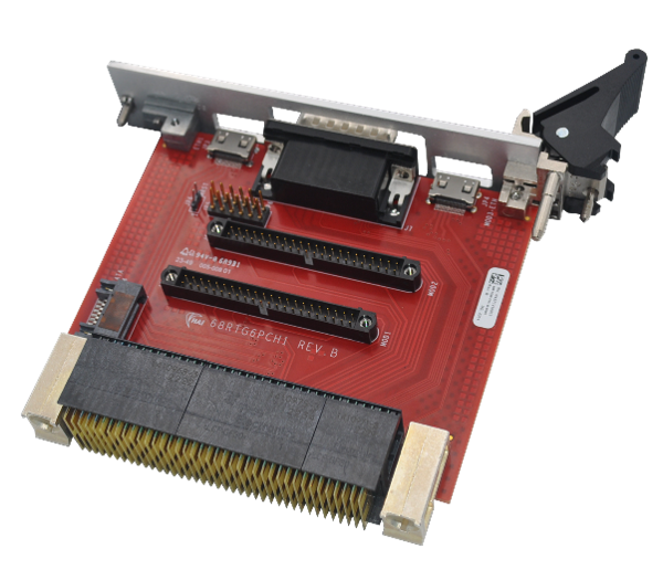
FUNCTION/FEATURES
- OpenVPX 1.0” pitch rear chassis I/O panel with IEEE 1101.10/11, Type IV, Injector/Ejector handle
- Optimized for NAI 68G6P MFIO-Processor board configured with Chassis Manager (CH1) module
- Industry standard commercial connectors, where applicable
DESCRIPTION
The 68RTG6P-CH1 is a 3U OpenVPX Rear I/O Transition Module (RTM) specifically optimized for the 68G6P MFIO-Processor module (board) and is intended for use with modules requiring high-speed routing for Chassis Manager (CH1) functions. The 68RTG6P-CH1 is for use in OpenVPX systems/chassis with RTM accessibility that require reliable interconnection between the rear I/O P1 & P2 OpenVPX connectors and the ‘outside world’.
SPECIFICATIONS
| Operating Temperature: | 0°C to 70°C (typical usage, contact factory for extended temperature range) |
| Storage Temperature: | -40°C to 85°C |
| Humidity: | 95% RH, non-condensing |
| Protective Covering: | Both sides of the board are protected/covered with solder mask |
| I/O Connector Configuration: | Two mini-HDMI-type rear panel receptacles (JP3) (Motherboard Gig-E & serial RS-232 debug) and (JP4) (Chassis Manager Gig-E, USB UART, & serial RS-232 debug) One inboard I/O connector (J4), SATA Two inboard function module 44-pin module function I/O Header (J5, J6) One panel 26-pin chassis manager I/O function connector (J7) One inboard 6x2, 0.10”, Vertical Header for GPIO/TTL One inboard 1x2, 0.05", Vertical Headers for signal shunts. |
| Size: | 3U height, 4HP width (100 mm H x 20.3 mm W x 80 mm D) / 5HP (1.0”) width option |
| Weight: | 4 oz. (113 g) (approx.) |
| Mini-HDMI Panel Receptacle: | Mini-HDMI (19 position) type-A receptacle (MHDMR-19-02-H-TH-L-TR, Samtec). |
| Mini-HDMI Mate Kit: | Cable assembly/breakout board adapter kit (not supplied – optional): May be purchased separately under NAI P/N 75SBC4-BB (Contact Factory). 75SBC4-BB Includes: a. MHDMR-USB-ETH-SER-B003 breakout board b. NAI P/N 07-0030 (Cable Assy. (@ 1 m), (MHDMP to MHDMP) |
68RTG6P-CH1 INSTALLATION
Note
For reference only.
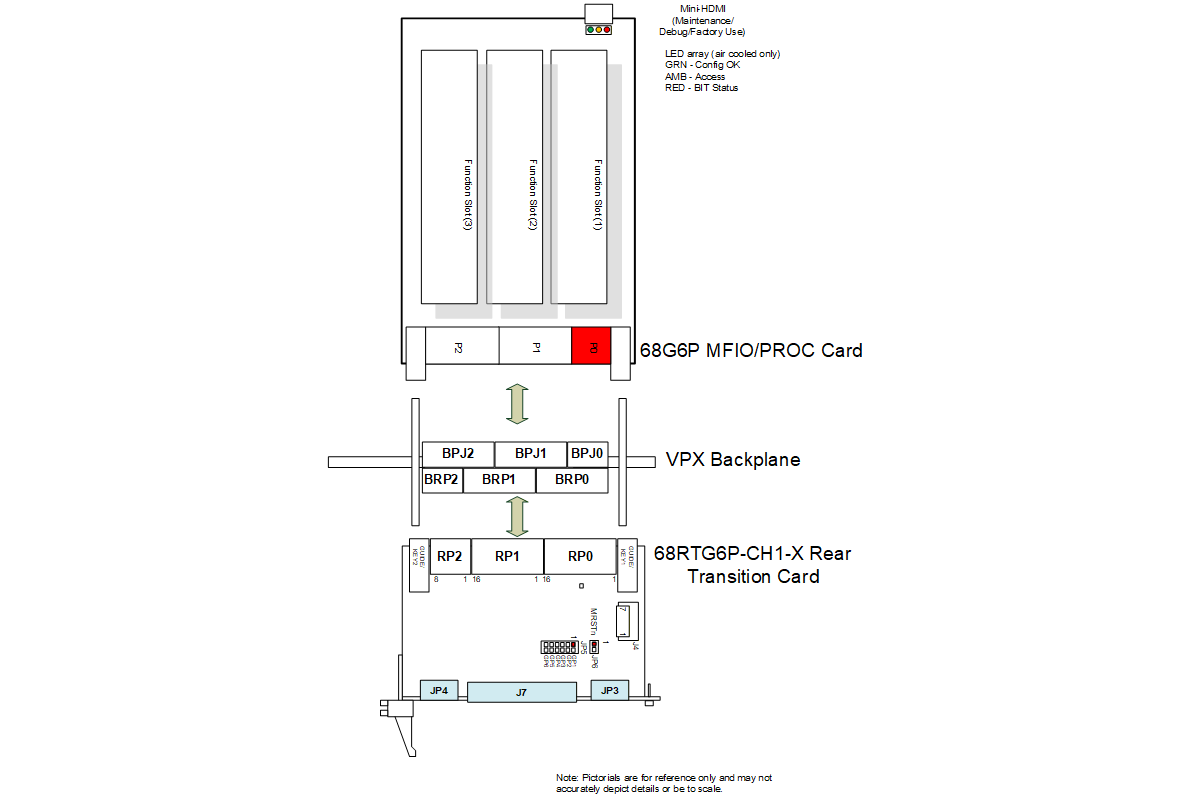
68RTG6P-CH1 CONNECTOR/PIN-OUT INFORMATION
I/O Connectors
User and defined I/O is available through panel mounted and in-board header connectors via the VPX RP0, RP1 & RP2 user defined rear I/O backplane connectors. The 68RTG6P-CH1 RTM is optimized for use for the 68G6P with a CH1 module in module slot 3. Please reference additional information and documentation from the respective 68G6 board web product page(s).
Caution
Do not connect to any undesignated or n/c pins.
Note
The following notes apply unless otherwise specified:
- Maximum ratings for the VPX MultiGig-RT2 type rear I/O connectors are as follows (per TE connectivity 108-2072, Rev F):
• Operating Voltage: 166 volts AC peak or DC
• Current: Signal Wafers: 1.5 ampere at <30°C (Single circuit, free air)- Signal names are provided for reference (referenced to 68G6P-CH1 or 68RTG6P-CH1 signal names) only.
RTM Panel Connector System Ground Pins
See specific connector, header, or receptacle pinout.
RTM Panel Connector Chassis Grounding Pins
Panel: No dedicated chassis GND pins available.
Once installed and secured within a VPX chassis, the panel itself, rear VPX connector key guides and panel receptacle shell are connected to chassis.
RTM REAR I/O (BACKPLANE DEFINED) PINOUTS
RTM VPX RP0 w1-8 I/O Definition (68G6P-CH1 PIC P0)
| UTILITY | Row | Row | Row | Row | Row | Row | Row | |
| P0 | RTM REF | G | F | E | D | C | B | A |
| 1 | RP0x-01 | n/c (+12V (VS1)) | n/c (+12V (VS1)) | n/c (+12V (VS1)) | n/c (NCD1) | n/c (VS2) | n/c (VS2) | n/c (VS2) |
| 2 | RP0x-02 | n/c (+12V (VS1)) | n/c (+12V (VS1)) | n/c (+12V (VS1)) | n/c (NCD2) | n/c (VS2) | n/c (VS2) | n/c (VS2) |
| 3 | RP0x-03 | n/c (VS3) | n/c (VS3) | n/c (VS3) | n/c (NCD3) | n/c (VS3) | n/c (VS3) | n/c (VS3) |
| 4 | RP0x-04 | n/c (IMPB-SCL-B) | n/c (IMPB-SDA-B) | GND | n/c (-12V AUX) | GND | n/c (P0-SYSRSTn) | n/c (NVMRO) |
| 5 | RP0x-05 | n/c (P0-GAPn) | n/c (P0-GA4n) | GND | n/c (+3.3V_AUX) | GND | n/c (IMPB-SCL-A) | n/c (IMPB-SDA-A) |
| 6 | RP0x-06 | n/c (P0-GA3n) | n/c (P0-GA2n) | GND | n/c (+12V_AUX) | GND | n/c (P0-GA1n) | n/c (P0-GA0n) |
| 7 | RP0x-07 | n/c (TCK) | GND | n/c (TDO) | n/c (TDI) | GND | n/c (TMS) | n/c (TRST) |
| 8 | RP0x-08 | GND | n/c (REFCLK-25MHz-) | n/c (REFCLK-25MHz+) | GND | n/c (AUX-CLK-) | n/c (AUX-CLK+) | GND |
RTM VPX RP0 w9-16 & RP1 w1-8 I/O Definition (68G6P-CH1 PIC J1)
| Plug-In Card P1 | Row G | Row F | Row E | Row D | Row C | Row B | Row A | |||
| Even | Odd | Even | Odd | |||||||
| Backplane J1 | RTM REF | Row i | Row h | Row g | Row f | Row e | Row d | Row c | Row b | Row a |
| 1 | RP0x-09 | n/c (GDiscrete1) | GND | GND-J1 | n/c (BP_PCIE1_RX_N) | n/c (BP_PCIE1_RX_P) | GND | GND-J1 | n/c (PCIE_RX8_N) | n/c (PCIE_RX8_P) |
| 2 | RP0x-10 | GND | n/c (BP_PCIE2_RX_N) | n/c (BP_PCIE2_RX_P) | GND-J1 | GND | n/c (PCIE_RX9_N) | n/c (PCIE_RX9_P) | GND-J1 | GND |
| 3 | RP0x-11 | n/c (P1-VBAT) | GND | GND-J1 | n/c (USB_RX_N) | n/c (USB_RX_P) | GND | GND-J1 | n/c (PS_USB3_TX_N) | n/c (PS_USB3_TX_P) |
| 4 | RP0x-12 | GND | MOD1_DATIO32 | MOD1_DATIO31 | GND-J1 | GND | MOD1_DATIO30 | MOD1_DATIO29 | GND-J1 | GND |
| 5 | RP0x-13 | n/c (SYS_CON*) | GND | GND-J1 | MOD1_DATIO28 | MOD1_DATIO27 | GND | GND-J1 | MOD1_DATIO26 | MOD1_DATIO25 |
| 6 | RP0x-14 | GND | MOD1_DATIO24 | MOD1_DATIO23 | GND-J1 | GND | MOD1_DATIO22 | MOD1_DATIO21 | GND-J1 | GND |
| 7 | RP0x-15 | n/c (+5V0_USB) | GND | GND-J1 | MOD1_DATIO20 | MOD1_DATIO19 | GND | GND-J1 | MOD1_DATIO18 | MOD1_DATIO17 |
| 8 | RP0x-16 | GND | MOD1_DATIO16 | MOD1_DATIO15 | GND-J1 | GND | MOD1_DATIO14 | MOD1_DATIO13 | GND-J1 | GND |
| 9 | RP1x-01 | RS-232 Rx | GND | GND-J1 | SATA_MOD2_TX_N | SATA_MOD2_TX_P | GND | GND-J1 | SATA_MOD2_RX_N | SATA_MOD2_RX_P |
| 10 | RP1x-02 | GND | MOD1_DATIO12 | MOD1_DATIO11 | GND-J1 | GND | MOD1_DATIO10 | MOD1_DATIO09 | GND-J1 | GND |
| 11 | RP1x-03 | RS-232 Tx | GND | GND-J1 | MOD1_DATIO08 | MOD1_DATIO07 | GND | GND-J1 | MOD1_DATIO06 | MOD1_DATIO05 |
| 12 | RP1x-04 | GND | MOD1_DATIO4 | MOD1_DATIO3 | GND-J1 | GND | MOD1_DATIO02 | MOD1_DATIO01 | GND-J1 | GND |
| 13 | RP1x-05 | TTL1 | GND | GND-J1 | MB_ETHB_TP1_N | MB_ETHB_TP1_P | GND | GND-J1 | MB_ETHB_TP0_N | MB_ETHB_TP0_P |
| 14 | RP1x-06 | GND | MB_ETHB_TP3_N | MB_ETHB_TP3_P | GND-J1 | GND | MB_ETHB_TP2_N | MB_ETHB_TP2_P | GND-J1 | GND |
| 15 | RP1x-07 | M_Reset* | GND | GND-J1 | n/c (KR_TX1_N) | n/c (KR_TX1_P) | GND | GND-J1 | n/c (KR_RX1_N) | n/c (KR_RX1_P) |
| 16 | RP1x-08 | GND | n/c (KR_TX0_N) | n/c (KR_TX0_P) | GND-J1 | GND | n/c (KR_RX0_N) | n/c (KR_RX0_P) | GND-J1 | GND |
RTM VPX RP1 w9-16 & RP2 w1-8 I/O Definition (68G6P-CH1 PIC J2)
| Plug-In Card P2 | Row G | Row F | Row E | Row D | Row C | Row B | Row A | |||
| Even | Odd | Even | Odd | |||||||
| Backplane J2 | RTM REF | Row i | Row h | Row g | Row f | Row e | Row d | Row c | Row b | Row a |
| 1 | RP1x-09 | TTL5 | GND | GND-J2 | MOD2_DATIO32 | MOD2_DATIO31 | GND | GND-J2 | MOD2_DATIO30 | MOD2_DATIO29 |
| 2 | RP1x-10 | GND | MOD2_DATIO28 | MOD2_DATIO27 | GND-J2 | GND | MOD2_DATIO26 | MOD2_DATIO25 | GND-J2 | GND |
| 3 | RP1x-11 | TTL6 | GND | GND-J2 | MOD2_DATIO24 | MOD2_DATIO23 | GND | GND-J2 | MOD2_DATIO22 | MOD2_DATIO21 |
| 4 | RP1x-12 | GND | MOD2_DATIO20 | MOD2_DATIO19 | GND-J2 | GND | MOD2_DATIO18 | MOD2_DATIO17 | GND-J2 | GND |
| 5 | RP1x-13 | N/C | GND | GND-J2 | MOD2_DATIO16 | MOD2_DATIO15 | GND | GND-J2 | MOD2_DATIO14 | MOD2_DATIO13 |
| 6 | RP1x-14 | GND | MOD2_DATIO12 | MOD2_DATIO11 | GND-J2 | GND | MOD2_DATIO10 | MOD2_DATIO9 | GND-J2 | GND |
| 7 | RP1x-15 | N/C | GND | GND-J2 | MOD2_DATIO8 | MOD2_DATIO07 | GND | GND-J2 | MOD2_DATIO6 | MOD2_DATIO5 |
| 8 | RP1x-16 | GND | MOD2_DATIO4 | MOD2_DATIO3 | GND-J2 | GND | MOD2_DATIO2 | MOD2_DATIO1 | GND-J2 | GND |
| 9 | RP2x-01 | N/C | GND | GND-J2 | REDUN COUT | REDUN CIN | GND | GND-J2 | THERMISTOR | LED PWR |
| 10 | RP2x-02 | GND | MRI RXD | MRI TXD | GND-J2 | GND | CMM RESET IN | SYSRESETn | GND-J2 | GND |
| 11 | RP2x-03 | TTL2 | GND | GND-J2 | CHM_CONSOLE_TXD | CHM_CONSOLE_RXD | GND | GND-J2 | LED OVERTEMPn | LED FAN FAILn |
| 12 | RP2x-04 | GND | PS INHIBITn | PS FAIL | GND-J2 | GND | GND | ChMC GPIO | GND-J2 | GND |
| 13 | RP2x-05 | TTL3 | GND | GND-J2 | TACH2 | PWM2 | GND | GND-J2 | TACH1 | PWM1 |
| 14 | RP2x-06 | GND | GND | CH-USBP | GND-J2 | GND | CH-USBN | +5VUSB | GND-J2 | GND |
| 15 | RP2x-07 | TTL4 | GND | GND-J2 | M3_ETH0_TP3_N | M3_ETH0_TP3_P | GND | GND-J2 | M3_ETH0_TP2_N | M3_ETH0_TP2_P |
| 16 | RP2x-08 | GND | M3_ETH0_TP1_N | M3_ETH0_TP1_P | GND-J2 | GND | M3_ETH0_TP0_N | M3_ETH0_TP0_P | GND-J2 | GND |
RTM CONNECTORS GENERAL POSITIONING, LAYOUT, & PINOUT
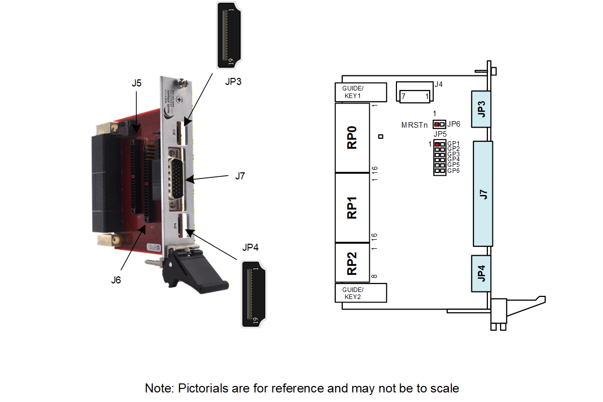
Mini-HDMI-Type JP3 & JP4 I/O Connectors Pin Mapping
MFG: MHDMR-19-02-H-TH-L-TR, Samtec (or equivalent)
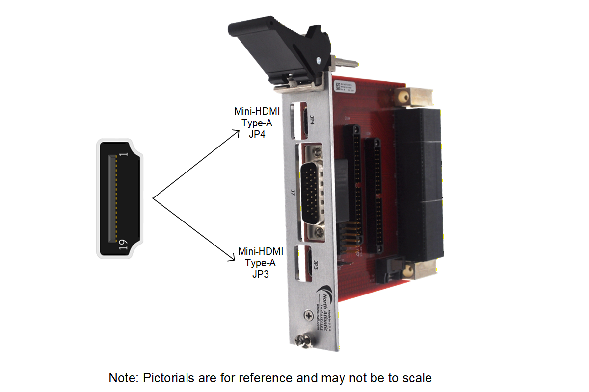
68RTG6P-CH1 JP3/JP4 Mini-HDMI (Front Debug)
68RTG6P-CH1 JP3 Mini-HDMI-Type receptacle I/O
| VPX | Signal (REF) | MINI-HDMI-type JP3 |
| N/C | 1 | |
| P1-A13 | ETH(B)-TP0+ | 2 |
| P1-B13 | ETH(B)-TP0- | 3 |
| N/C | 4 | |
| P1-D13 | ETH(B)-TP1+ | 5 |
| P1-E13 | ETH(B)-TP1- | 6 |
| N/C | 7 | |
| P1-B14 | ETH(B)-TP2+ | 8 |
| P1-C14 | ETH(B)-TP2- | 9 |
| N/C | 10 | |
| P1-E14 | ETH(B)-TP3+ | 11 |
| P1-F14 | ETH(B)-TP3- | 12 |
| GND | 13 | |
| N/C | 14 | |
| N/C | 15 | |
| N/C | 16 | |
| P1-G9 | (SER-RXD) | 17 |
| P1-G11 | (SER-TXD) | 18 |
| GND | 19 |
KEY
| = Eth Port / 10/100/1000Base-T (option) | |
| = Maintenance (reserved) |
Commercial RJ45 Equivalent
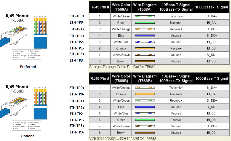
68RTG6P-CH1 JP4 Mini-HDMI-Type receptacle I/O
| VPX RP | Signal (REF) | MINI-HDMI-type JP4 |
| N/C | 1 | |
| RP2-B8 | MOD3-ETH0-TP0+ | 2 |
| RP2-C8 | MOD3-ETH0-TP0- | 3 |
| N/C | 4 | |
| RP2-E8 | MOD3-ETH0-TP1+ | 5 |
| RP2-F8 | MOD3-ETH0-TP1- | 6 |
| N/C | 7 | |
| RP2-A7 | MOD3-ETH0-TP2+ | 8 |
| RP2-B7 | MOD3-ETH0-TP2- | 9 |
| N/C | 10 | |
| RP2-D7 | MOD3-ETH0-TP3+ | 11 |
| RP2-E7 | MOD3-ETH0-TP3- | 12 |
| GND | 13 | |
| RP2-B6 | +5VUSB | 14 |
| RP2-E6 | CH-USB+ | 15 |
| RP2-C6 | CH-USB- | 16 |
| RP2-D3 | CHM_CONSOLSE_RXD | 17 |
| RP2-E3 | CHM_CONSOLE_TXD | 18 |
| GND | 19 |
Inboard Connections
J4, MOD-2 SATA
MFG: 47080-4005, Molex; 7 Position SATA Plug, Shrouded Connector Solder Surface Mount, Right Angle
Utilized for SATA SSD access from a 68G6P-CH1 when properly configured with an FMx SATA SSD function module in module slot 2.
JP5, JP6 Header/Shunts
JP5: MFG: TSM-106-02-T-DV-P-TR, SAMTEC; HDR, 6x2, 0.100, Vertical, SM
JP6: MFG: TMS-101-51-T-D, SAMTEC; HDR,1x2, 0.05”, Vertical, TH
JP5 is utilized for access to GPIO/TTL type signals (available only if the 68G6P board is appropriately configured).
JP6 is utilized for board reset input. Momentary; short and release initiates 68G6P motherboard reset.
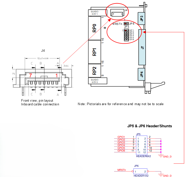
68RTG6P-CH1 J4 SATA Data
| VPX PIC | Signal (REF) | SATA J4 |
| GND | 1 | |
| RP1-D1 | SATA_MOD2_TX_P | 2 |
| RP1-E1 | SATA_MOD2_TX_N | 3 |
| GND | 4 | |
| RP1-B1 | SATA_MOD2_RX_N | 5 |
| RP1-A1 | SATA_MOD2_RX_P | 6 |
| GND | 7 |
J5 & J6, Inboard Module Function I/O Connector Interfaces
Two inboard 44-pin Header, Module Standard I/O interface (J5, J6)
M80-5114422, Harwin; CONN, 44Pin, Male, Vertical, 2MM Spacing, or equivalent
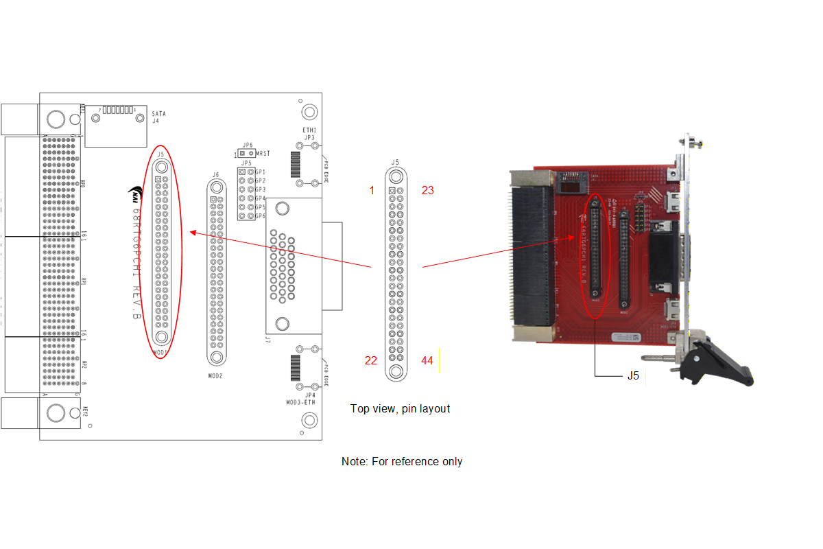
68RTG6P-CH1 J5 (M1) Inboard Module Standard I/O
| VPX RP | J5 Inboard I/O | VPX RP | |||
| GND | 1 | 23 | GND | ||
| RP1-B4 | MOD1-DATIO01 | 2 | 24 | MOD1-DATIO02 | RP1-C4 |
| RP1-E4 | MOD1-DATIO03 | 3 | 25 | MOD1-DATIO04 | RP1-F4 |
| RP0-A13 | MOD1-DATIO25 | 4 | 26 | MOD1-DATIO26 | RP0-B13 |
| RP1-A3 | MOD1-DATIO05 | 5 | 27 | MOD1-DATIO06 | RP1-B3 |
| n/c | 6 | 28 | n/c | ||
| RP1-D3 | MOD1-DATIO07 | 7 | 29 | MOD1-DATIO08 | RP1-E3 |
| RP1-B2 | MOD1-DATIO09 | 8 | 30 | MOD1-DATIO10 | RP1-C2 |
| RP0-D13 | MOD1-DATIO27 | 9 | 31 | MOD1-DATIO28 | RP0-E13 |
| RP1-E2 | MOD1-DATIO11 | 10 | 32 | MOD1-DATIO12 | RP1-F2 |
| n/c | 11 | 33 | n/c | ||
| RP0-B16 | MOD1-DATIO13 | 12 | 34 | MOD1-DATIO14 | RP0-C16 |
| RP0-E16 | MOD1-DATIO15 | 13 | 35 | MOD1-DATIO16 | RP0-F16 |
| RP0-B12 | MOD1-DATIO29 | 14 | 36 | MOD1-DATIO30 | RP0-C12 |
| RP0-A15 | MOD1-DATIO17 | 15 | 37 | MOD1-DATIO18 | RP0-B15 |
| n/c | 16 | 38 | n/c | ||
| RP0-D15 | MOD1-DATIO19 | 17 | 39 | MOD1-DATIO20 | RP0-E15 |
| RP0-B14 | MOD1-DATIO21 | 18 | 40 | MOD1-DATIO22 | RP0-C14 |
| RP0-E12 | MOD1-DATIO31 | 19 | 41 | MOD1-DATIO32 | RP0-F12 |
| RP0-E14 | MOD1-DATIO23 | 20 | 42 | MOD1-DATIO24 | RP0-F14 |
| n/c | 21 | 43 | n/c | ||
| n/c | 22 | 44 | n/c | ||
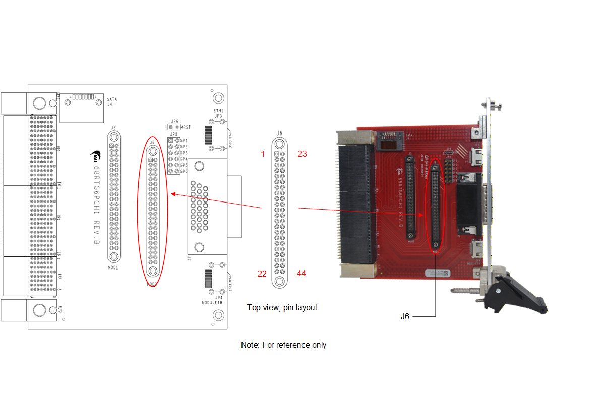
68RTG6P-CH1 J6 (M2) Inboard Module Standard I/O
| VPX RP | J6 Inboard I/O | VPX RP | |||
| GND | 1 | 23 | GND | ||
| RP1-B16 | MOD2-DATIO01 | 2 | 24 | MOD2-DATIO02 | RP1-C16 |
| RP1-E16 | MOD2-DATIO03 | 3 | 25 | MOD2-DATIO04 | RP1-F16 |
| RP1-B10 | MOD2-DATIO25 | 4 | 26 | MOD2-DATIO26 | RP1-C10 |
| RP1-A15 | MOD2-DATIO05 | 5 | 27 | MOD2-DATIO06 | RP1-B15 |
| n/c | 6 | 28 | n/c | ||
| RP1-D15 | MOD2-DATIO07 | 7 | 29 | MOD2-DATIO08 | RP1-E15 |
| RP1-B14 | MOD2-DATIO09 | 8 | 30 | MOD2-DATIO10 | RP1-C14 |
| RP1-E10 | MOD2-DATIO27 | 9 | 31 | MOD2-DATIO28 | RP1-F10 |
| RP1-E14 | MOD2-DATIO11 | 10 | 32 | MOD2-DATIO12 | RP1-F14 |
| n/c | 11 | 33 | n/c | ||
| RP1-A13 | MOD2-DATIO13 | 12 | 34 | MOD2-DATIO14 | RP1-B13 |
| RP1-D13 | MOD2-DATIO15 | 13 | 35 | MOD2-DATIO16 | RP1-E13 |
| RP1-A9 | MOD2-DATIO29 | 14 | 36 | MOD2-DATIO30 | RP1-B9 |
| RP1-B12 | MOD2-DATIO17 | 15 | 37 | MOD2-DATIO18 | RP1-C12 |
| n/c | 16 | 38 | n/c | ||
| RP1-E12 | MOD2-DATIO19 | 17 | 39 | MOD2-DATIO20 | RP1-F12 |
| RP1-A11 | MOD2-DATIO21 | 18 | 40 | MOD2-DATIO22 | RP1-B11 |
| RP1-D9 | MOD2-DATIO31 | 19 | 41 | MOD2-DATIO32 | RP1-E9 |
| RP1-D11 | MOD2-DATIO23 | 20 | 42 | MOD2-DATIO24 | RP1-E11 |
| n/c | 21 | 43 | n/c | ||
| n/c | 22 | 44 | n/c | ||
J7, Chassis Manager I/O
One panel H/D D-SUB Connector, 26Pin, Male, RT Angle, Th
10090926-P26XLF, Amphenol (or equivalent)
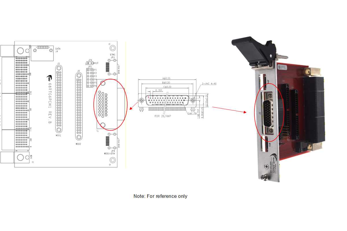
68RTG6P-CH1 J7 H/D D-Sub Connector
| VPX RP | Signal (REF) | H/D D-Sub J7 |
| RP2-A1 | LED PWR | 1 |
| RP2-A3 | LED FAN FAILn | 2 |
| RP2-B3 | LED OVERTEMPn | 3 |
| RP2-B1 | THERMISTOR | 4 |
| RP2-B2 | SYSRESETn | 5 |
| RP2-A5 | PWM1 | 6 |
| RP2-B5 | TACH1 | 7 |
| RP2-D5 | PWM2 | 8 |
| RP2-E5 | TACH2 | 9 |
| RP2-B4 | ChMC GPIO | 10 |
| RP2-C2 | CMM RESET IN | 11 |
| RP2-D1 | REDUN CIN | 12 |
| RP2-E1 | REDUN COUT | 13 |
| RP2-E2 | MRI TXD | 14 |
| RP2-F2 | MRI RXD | 15 |
| RP2-E4 | PS FAIL | 16 |
| RP2-F4 | PS INHIBITn | 17 |
| GND | 18 | |
| n/c | 19 | |
| n/c | 20 | |
| n/c | 21 | |
| n/c | 22 | |
| n/c | 23 | |
| n/c | 24 | |
| n/c | 25 | |
| n/c | 26 |
PART NUMBER DESIGNATION
68RTG6P-CH1-X is used/referenced to:
Standard Product Part Number(s): 68RTG6P-CH1-X
| X | = Configuration Options |
| 1 | • Supports standard function (3) module I/O & routing. |
| TBD | = Other than listed; indicates custom configuration - Contact Factory |
Specifications are subject to change without notice.
REVISION HISTORY
| 68RTG6P-CH1 Manual Revision History | ||
| Revision | Revision Date | Description |
| A | 2024-06-27 | ECO C11667, initial release of 68RTG6P-CH1 OpenVPX RTM data sheet. |
DOCS.NAII REVISIONS
| Revision Date | Description |
|---|---|
| 2026-08-20 | Updated documentation to docs.naii format. |
NAI Cares
North Atlantic Industries (NAI) is a leading independent supplier of Embedded I/O Boards, Single Board Computers, Rugged Power Supplies, Embedded Systems and Motion Simulation and Measurement Instruments for the Military, Aerospace and Industrial Industries. We accelerate our clients’ time-to-mission with a unique approach based on a Configurable Open Systems Architecture™ (COSA®) that delivers the best of both worlds: custom solutions from standard COTS components.
We have built a reputation by listening to our customers, understanding their needs, and designing, testing and delivering board and system-level products for their most demanding air, land and sea requirements. If you have any applications or questions regarding the use of our products, please contact us for an expedient solution.
Please visit us at: www.naii.com or select one of the following for immediate assistance:
Documentation
FAQ
Application Notes
http://www.naii.com/applicationnotes
Calibration and Repairs
http://www.naii.com/calibrationrepairs
Call Us
(631) 567-1100
Link to original