Introduction
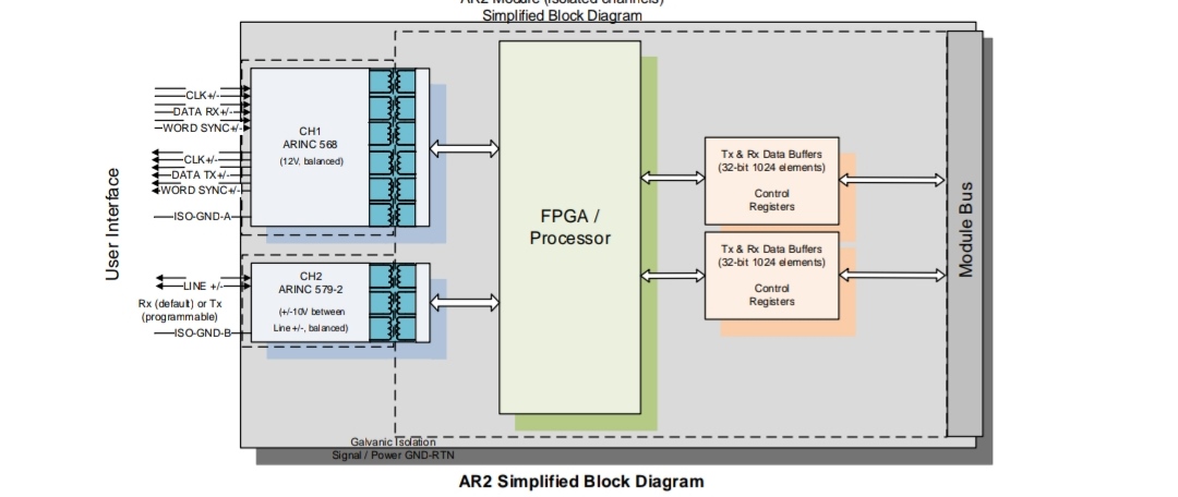
This module manual provides information about the North Atlantic Industries, Inc. (NAI) ARINC 568/579 Communications Function Module: AR2. This module is compatible with all NAI Generation 5 motherboards. The AR2 provides a combined function for two ARINC-specific serial interfaces. The primary function is to “receive” serial communications per the ARINC 568 (CH-1) & 579-2 (CH-2) digital serial communications interfaces. Secondary function is to “transmit” (simulate) messages. The channels can transmit or receive, but not expected to occur simultaneously (the channels can be programmed operated in Receive (default) or Transmit modes). Point-to-Point connection only (multi-drop not expected).
ARINC 568 is a data transfer standard for aircraft avionics. The data transmission system consists of three twowire (twisted and shielded pair) circuits. The function of the circuits is serial data transmission, word synchronization and clock. The data word is 32 bits in length. Messages are transmitted at 11 kbps to other system elements that monitor the bus messages.
ARINC 579 is a data transfer standard for aircraft avionics. It uses a self-clocking and self-synchronizing data bus protocol. The physical connection wires are twisted pairs carrying balanced differential signaling. Data words are 32 bits in length and most messages consist of a single data word. Messages are transmitted at 11 kbps to other system elements that monitor the bus messages.
Features
• Receive/Transmit mode programmable channel (ARINC-579) • Separate Receive and Transmit channel (ARINC-568) • 11 kHz transmission rate • Programmable gap times • Transmit: 1024-word FIFO per channel • Receive: 1024-word FIFO per channel • Selectable hardware parity generation/checking • Receive time stamping • Continuous BIT • Loop-back test • Tri-state outputs • High and Low Speed Slew Rate outputs
Specifications
Module AR2 – ARINC 568 & 579-2 Communications Interface
ARINC 568
| Number of Channels: | One channel Rx and Tx (independent signal lines) |
|---|---|
| Hardware Interface: (per channel, unless otherwise specified) | Appropriate HW interface per ARINC 568 specification (see following) • 3 differential pairs (6-wire; CLK±, DATA± and Word Sync±, 12V nominal) plus ISOGND REF • Clock (input for receiver, output for transmitter) @ 11 ±3.5 kHz |
| Protocol: | No protocol label/address distinction. • 32-bit “words” only; application software is expected to parse out address, etc. from data as needed. |
| Receive/Transmit Buffers: | 32-bit data buffer / 1024 deep |
| FIFO Buffer Functions | • Data “watermark” and other FIFO control/interrupt abilities • Circular FIFO (default) and FIFO-Full modes. |
ARINC 579-2
| Number of Channels: | One channel Rx or Tx (programmable; Rx default) |
|---|---|
| Hardware Interface: (per channel, unless otherwise specified) | Appropriate HW interface per ARINC 579-2 specification (see following) • 1 differential pair (2-wire; Line /-, /-10V nominal) plus ISO-GND REF • Clock (data is contained in a self-synchronizing wave-form @ 11 +/- 3.5 kHz) |
| Protocol: | No protocol label/address distinction. • 32-bit “words” only; application software is expected to parse out address, etc. from data as needed. |
| Receive/Transmit Buffers: | 32-bit data buffer / 1024 deep |
| FIFO Buffer Functions | • Data “watermark” and other FIFO control/interrupt abilities • Circular FIFO (default) and FIFO-Full modes. |
General
| Power | 5 VDC @ 260 mA (est. typical) |
|---|---|
| Weight | 1.5 oz. (42 g) (est.) |
| Ground | Isolated to 250 V (min.), from system GND and Chassis (applies to each channel). |
Specifications By Mode
| Specifications | ARINC 568 | ARINC 579 |
|---|---|---|
| Mode of Operation | Differential | Differential |
| Data Rate | 11 kHz | 11 kHz |
| Driver Output Signal Level (Min Loaded) | 0-12V | ±10.0V |
| Receiver Input Voltage Range | -25V to +25V | -17V to +17V |
| Receiver Input Resistance (Ohms) | 28K |
Module Factory Defaults
| Speed: | 11 kHz |
|---|---|
| Gap Time: | 4 bits |
| Mode: | FIFO |
| Parity (Odd): | Enabled |
| Timestamp | Disabled |
| Receivers: | Disabled |
| Transmitters: | Disabled |
| Number of Words TX Buffer: | 0 |
| Number of Words RX Buffer: | 0 |
| Rx Buffer, Almost Full: | 0x80h |
| Tx Buffer, Almost Empty: | 0x20h |
| Tx-Rx Configuration: | 0 |
| Channel Control: | 0 |
| BIT Threshold: | 0x1000 |
Principle of Operation – ARINC568
Module AR2 provides one ARINC-568 receive channel and one ARINC-568 transmit channel. The channel is software selectable for transmit and/or receive and odd or no parity.
Receive Operation
The data transmission system consists of three two-wire (twisted and shielded pair) circuits. The function of the circuits is serial data transmission, word synchronization and clock. The clock is input at 11 kbps to the receiver and used for data bit capture. To simplify data reception, a word synchronization input is used. The word synchronization bit will transition to a logic high beginning simultaneously with the first bit on the data line. The data word is 32 bits in length. The first eight bits are the address or label. The word sync is interrupted for ½ bit during the last one-half of the eighth data bit (end of the address/label field) to provide a data gate signal. The remaining 24 bits are transferred as data. The word sync returns to zero with the end of the last data field bit. The FIFO can be set to either bounded or circular(default) mode. In bounded mode, the FIFO will not accept any additional data once it is full. In circular mode, once the FIFO is full, additional writes replace the oldest data value. The FIFO will remain full, until read or reset, but new data will overwrite the older data.
Principle of Operation – ARINC579
Transmit Operation
Transmitters are tri-stated when TX is not enabled. Transmit operates in one of two modes: Immediate FIFO, Triggered FIFO. In immediate mode, ARINC-568 data is sent as soon as data is written to the transmit FIFO. In Triggered FIFO mode, a write to the trigger register is needed to start transmission of the transmit FIFO contents. Transmission continues until the FIFO is empty. To transmit more data after the FIFO empties out, issue a new trigger after filling the transmit FIFO with new data. The FIFO can be set to either bounded or circular(default) mode. In full mode, the FIFO will not accept any additional data once it is full. In circular mode, once the FIFO is full, additional writes replace the oldest data value. The FIFO will remain full, until read or reset, but new data will overwrite the older data. For either FIFO mode, a gap of one-bit time, the minimum allowed, is used.
Built-In-Test
The BIT section consists of two subsections. A BIT clock circuit that checks the clock and the BIT clock for transitions using an edge watchdog. If an edge is not detected within 320 µs, a status bit is set in the status register. A BIT error is not set for a missing clock. Once the clock is deemed valid, BIT tests are started. In Transmit operations, internal transmit data is compared to loop-back data received by the receivers on a word by word basis. If the data does not match, a BIT counter is incremented by two. If the data does match, a BIT counter is decremented by one. The BIT counter threshold value is defaulted to 4096(d). If the BIT counter exceeds the BIT threshold register, the BIT ERROR bit is set and held in the bit status register and channel status register and/or an interrupt is generated if enabled. If the BIT counter drops below the BIT Threshold, the BIT ERROR bit will be cleared. BIT is only active if the channel RX or TX is enabled. Receive operations work in the same way, except that two receiver circuits acquire the data on a word by word basis.
Principle of Operation – ARINC579
Module AR2 provides one programmable ARINC-579 channel. The channel is software selectable for transmit and/or receive and odd or no parity.
Receive Operation
Serial BRZ data is decoded for logic states: one, zero or null. Once Word Gap is detected (4 null states) the receiver waits for either a zero or one state to start the serial-to-parallel shift function. If a waveform timing fault is detected before the serial/parallel function is complete, operation is terminated and the receiver returns to waiting for Word Gap detection. The serial-to-parallel output data is validated for odd parity. The message is stored in the receive FIFO. The FIFO can be set to either bounded mode or circular(default) mode. In bounded mode, the FIFO will not accept any additional data once it is full. In circular mode, once the FIFO is full, additional writes replace the oldest data value. The FIFO will remain full, until read or reset, but new data will overwrite the older data. In FIFO extended write mode, received ARINC messages / words are stored with an associated status word and an optional time-stamp value in the channel’s receive FIFO. The status word indicates parity error.
Transmit Operation
Transmitters are tri-stated when TX is not enabled. Transmit operates in one of two modes: Immediate FIFO, Triggered FIFO. In immediate mode, ARINC data is sent as soon as data is written to the transmit FIFO. In
Triggered FIFO mode, a write to the trigger register is needed to start transmission of the transmit FIFO contents. Transmission continues until the FIFO is empty. To transmit more data after the FIFO empties out, issue a new trigger after filling the transmit FIFO with new data. The FIFO can be set to either bounded mode or circular(default) mode. In bounded mode, the FIFO will not accept any additional data once it is full. In circular mode, once the FIFO is full, additional writes replace the oldest data value. The FIFO will remain full, until read or reset, but new data will overwrite the older data. For either FIFO mode, a transmit FIFO Rate register is provided to control rate of transmission. The contents of this register specify the gap time between transmitted words from the FIFO. The default is the minimum ARINC-579 gap time of 4-bit times. Loop-Back
Transmit data is looped-back continuously through the unused receive logic of the same channel and is made available for user verification if the channel receiver is also enabled.
Register Descriptions
The register descriptions provide the register name, Function Address Offset, Type, Data Range, Read or Write information, Initialized Value, a description of the function and, in most cases, a data table. Note that the function name used on the software map, which may be different than the hardware name, is provided in parentheses in the Function Address Offset field.
Tx FIFO
Function: This register is the transmit data FIFO. In immediate or triggered FIFO modes, transmit data is placed here prior to transmission. ARINC data words are 32-bits.
Type: unsigned character word
Data Range: 0 to 0xFFFFFFFF
Read/Write: W
Initialized Value: N/A
Operational Settings: ARINC data words are 32-bits.
Tx FIFO
| REGISTER | D31 | D30 | D29 | D28 | D27 | D26 | D25 | D24 | D23 | D22 | D21 | D20 | D19 | D18 | D17 | D16 | FUNCTION |
|---|---|---|---|---|---|---|---|---|---|---|---|---|---|---|---|---|---|
| TRANSMIT FIFO | D | D | D | D | D | D | D | D | D | D | D | D | D | D | D | D | D=DATA BIT |
| REGISTER | D15 | D14 | D13 | D12 | D11 | D10 | D9 | D8 | D7 | D6 | D5 | D4 | D3 | D2 | D1 | D0 | FUNCTION |
| TRANSMIT FIFO | D | D | D | D | D | D | D | D | D | D | D | D | D | D | D | D | D=DATA BIT |
Rx FIFO
Function: In FIFO receive mode, the received ARINC messages are read back from here.
Type: unsigned integer word
Data Range: 0 to 0xFFFFFFFF
Read/Write: R
Initialized Value: N/A
Operational Settings: In normal mode, reads from this register retrieve the ARINC data word. In FIFO extended write mode, perform two reads from this register to retrieve the Status/timestamp word and the ARINC data word, respectively.
Rx FIFO
| REGISTER | D31 | D30 | D29 | D28 | D27 | D26 | D25 | D24 | D23 | D22 | D21 | D20 | D19 | D18 | D17 | D16 | FUNCTION |
|---|---|---|---|---|---|---|---|---|---|---|---|---|---|---|---|---|---|
| extended mode | 0 | BE | 1 | PE | T | T | T | T | T | T | T | T | T | T | T | T | Message Status/Timestamp |
| Normal/extended mode | D | D | D | D | D | D | D | D | D | D | D | D | D | D | D | D | Data Word |
| REGISTER | D15 | D14 | D13 | D12 | D11 | D10 | D9 | D8 | D7 | D6 | D5 | D4 | D3 | D2 | D1 | D0 | FUNCTION |
| extended mode | T | T | T | T | T | T | T | T | T | T | T | T | T | T | T | T | Message Status/Timestamp |
| Normal/extended mode | D | D | D | D | D | D | D | D | D | D | D | D | D | D | D | D | Data Word |
PE = Parity Error ‘1’ Calculated parity does not match the received parity bit BE = BIT Error ‘1’ BIT word did not match received word T = Timestamp 28-bit Timestamp value
Tx FIFO Almost Empty Value
Function: Specifies the level of the transmit buffer, equal or below, at which the Tx FIFO Almost Empty Status bits in the Latched Status and Dynamic Status registers are set.
Type: unsigned integer
Data Range: 0 to 1023
Read/Write: R/W
Initialized Value: 0x20 (32)
Operational Settings: This register is not reset by a channel reset.
Tx FIFO Almost Empty Value
| REGISTER | D31 | D30 | D29 | D28 | D27 | D26 | D25 | D24 | D23 | D22 | D21 | D20 | D19 | D18 | D17 | D16 | FUNCTION |
|---|---|---|---|---|---|---|---|---|---|---|---|---|---|---|---|---|---|
| Tx BUFFER AE VALUE | X | X | X | X | X | X | X | X | X | X | X | X | X | X | X | X | D=DATA BIT |
| REGISTER | D15 | D14 | D13 | D12 | D11 | D10 | D9 | D8 | D7 | D6 | D5 | D4 | D3 | D2 | D1 | D0 | FUNCTION |
| Tx BUFFER AE VALUE | X | X | X | X | X | D | D | D | D | D | D | D | D | D | D | D | D=DATA BIT |
Tx FIFO Almost Full Value
Function: Specifies the level of the transmit buffer, equal or above, at which the Tx FIFO Almost Full Status bits in the Latched Status and Dynamic Status registers are set.
Type: unsigned integer
Data Range: 0 to 1023
Read/Write: R/W Initialized Value*: 0x80 (128)
Operational Settings: This register is not reset by a channel reset.
Tx FIFO Almost Full Value
| REGISTER | D31 | D30 | D29 | D28 | D27 | D26 | D25 | D24 | D23 | D22 | D21 | D20 | D19 | D18 | D17 | D16 | FUNCTION |
|---|---|---|---|---|---|---|---|---|---|---|---|---|---|---|---|---|---|
| Tx BUFFER AF VALUE | X | X | X | X | X | X | X | X | X | X | X | X | X | X | X | X | D=DATA BIT |
| REGISTER | D15 | D14 | D13 | D12 | D11 | D10 | D9 | D8 | D7 | D6 | D5 | D4 | D3 | D2 | D1 | D0 | FUNCTION |
| Tx BUFFER AF VALUE | X | X | X | X | X | D | D | D | D | D | D | D | D | D | D | D | D=DATA BIT |
Rx FIFO Almost Empty Value
Function: Specifies the level of the receive buffer, equal or below, at which the Rx FIFO Almost Full Status bits in the Latched Status and Dynamic Status registers are set.
Type: unsigned integer
Data Range: 0 to 1023
Read/Write: R/W
Initialized Value: 0x20 (32)
Operational Settings: This register is not reset by a channel reset.
Rx FIFO Almost Empty Value
| REGISTER | D31 | D30 | D29 | D28 | D27 | D26 | D25 | D24 | D23 | D22 | D21 | D20 | D19 | D18 | D17 | D16 | FUNCTION |
|---|---|---|---|---|---|---|---|---|---|---|---|---|---|---|---|---|---|
| Rx BUFFER AE VALUE | X | X | X | X | X | X | X | X | X | X | X | X | X | X | X | X | D=DATA BIT |
| REGISTER | D15 | D14 | D13 | D12 | D11 | D10 | D9 | D8 | D7 | D6 | D5 | D4 | D3 | D2 | D1 | D0 | FUNCTION |
| Rx BUFFER AE VALUE | X | X | X | X | X | D | D | D | D | D | D | D | D | D | D | D | D=DATA BIT |
Rx FIFO Almost Full Value
Function: Specifies the level of the receive buffer, equal or above, at which the Rx FIFO Almost Full Status bits in the Latched Status and Dynamic Status registers are set.
Type: unsigned integer
Data Range: 0 to 1023
Read/Write: R/W
Initialized Value: 0x80 (128)
Operational Settings: This register is not reset by a channel reset.
Rx FIFO Almost Full Value
| REGISTER | D31 | D30 | D29 | D28 | D27 | D26 | D25 | D24 | D23 | D22 | D21 | D20 | D19 | D18 | D17 | D16 | FUNCTION |
|---|---|---|---|---|---|---|---|---|---|---|---|---|---|---|---|---|---|
| Rx BUFFER AF VALUE | X | X | X | X | X | X | X | X | X | X | X | X | X | X | X | X | D=DATA BIT |
| REGISTER | D15 | D14 | D13 | D12 | D11 | D10 | D9 | D8 | D7 | D6 | D5 | D4 | D3 | D2 | D1 | D0 | FUNCTION |
| Rx BUFFER AF VALUE | X | X | X | X | X | D | D | D | D | D | D | D | D | D | D | D | D=DATA BIT |
Tx FIFO Count
Function: Contains the number of ARINC 32-bit words in the transmit FIFO.
Type: unsigned integer word
Data Range: 0 to 1024
Read/Write: R
Initialized Value: 0
Operational Settings: Used only in FIFO transmit modes.
Tx FIFO Count
| REGISTER | D31 | D30 | D29 | D28 | D27 | D26 | D25 | D24 | D23 | D22 | D21 | D20 | D19 | D18 | D17 | D16 | FUNCTION |
|---|---|---|---|---|---|---|---|---|---|---|---|---|---|---|---|---|---|
| NUM WORDS TX BUFFER | X | X | X | X | X | X | X | X | X | X | X | X | X | X | X | X | D=DATA BIT |
| REGISTER | D15 | D14 | D13 | D12 | D11 | D10 | D9 | D8 | D7 | D6 | D5 | D4 | D3 | D2 | D1 | D0 | FUNCTION |
| NUM WORDS TX BUFFER | X | X | X | X | D | D | D | D | D | D | D | D | D | D | D | D | D=DATA BIT |
Rx FIFO Count
Function: Contains the number of words in the receive FIFO.
Type: unsigned integer word
Data Range: 0 to 1024
Read/Write: R
Initialized Value: 0
Operational Settings: If timestamp is disabled, the number of words will equal the number of ARINC data words. If timestamp is enabled, the number of words will be three per ARINC data words. One for the status, one for the ARINC message and one for the timestamp
Rx FIFO Count
| REGISTER | D31 | D30 | D29 | D28 | D27 | D26 | D25 | D24 | D23 | D22 | D21 | D20 | D19 | D18 | D17 | D16 | FUNCTION |
|---|---|---|---|---|---|---|---|---|---|---|---|---|---|---|---|---|---|
| NUM WORDS RX BUFFER | X | X | X | X | X | X | X | X | X | X | X | X | X | X | X | X | D=DATA BIT |
| REGISTER | D15 | D14 | D13 | D12 | D11 | D10 | D9 | D8 | D7 | D6 | D5 | D4 | D3 | D2 | D1 | D0 | FUNCTION |
| NUM WORDS RX BUFFER | X | X | X | X | D | D | D | D | D | D | D | D | D | D | D | D | D=DATA BIT |
Transmit Gap Time (AR579)
Function: Specifies gap time between transmitted messages.
Type: 32-bit unsigned integer
Data Range: 1-1023
Read/Write: R/W
Initialized Value: 4
Operational Settings: Each LSB is 1-bit time. Rates less than 4 are not valid for AR579.
Transmit Gap Time (AR579)
| REGISTER | D31 | D30 | D29 | D28 | D27 | D26 | D25 | D24 | D23 | D22 | D21 | D20 | D19 | D18 | D17 | D16 | FUNCTION |
|---|---|---|---|---|---|---|---|---|---|---|---|---|---|---|---|---|---|
| TRANSMIT GAP TIME | X | X | X | X | X | X | X | X | X | X | X | X | X | X | X | X | D=DATA BIT |
| REGISTER | D15 | D14 | D13 | D12 | D11 | D10 | D9 | D8 | D7 | D6 | D5 | D4 | D3 | D2 | D1 | D0 | FUNCTION |
| TRANSMIT GAP TIME | X | X | X | X | X | D | D | D | D | D | D | D | D | D | D | D | D=DATA BIT |
Timestamp Control Register (AR579)
Function: Determines the resolution of the timestamp counter.
Type: binary word
Data Range: not applicable
Read/Write: R/W
Initialized Value: 0x0000 (1 µs)
Operational Settings: The LSB can have one of four time values. Set bit D2 to 1 to zero out the timestamp counter. The default LSB value is 1 µs
Timestamp Control Register (AR579)
| REGISTER | D31 | D30 | D29 | D28 | D27 | D26 | D25 | D24 | D23 | D22 | D21 | D20 | D19 | D18 | D17 | D16 | FUNCTION |
|---|---|---|---|---|---|---|---|---|---|---|---|---|---|---|---|---|---|
| TIMESTAMP CONTROL | X | X | X | X | X | X | X | X | X | X | X | X | X | X | X | X | X |
| X | X | X | X | X | X | X | X | X | X | X | X | X | X | X | REGISTER | D15 | D14 |
| D13 | D12 | D11 | D10 | D9 | D8 | D7 | D6 | D5 | D4 | D3 | D2 | D1 | D0 | FUNCTION | TIMESTAMP CONTROL | X | X |
| X | X | X | X | X | X | X | X | X | X | X | X | D | D | RESOLUTION1 | X | X | X |
| X | X | X | X | X | X | X | X | X | X | 1 | X | X | ZERO TIMESTAMP2 |
Timestamp Register (AR579)
Function: Read current 28-bit timestamp value.
Type: unsigned integer
Data Range: 0 to 0xFFFFFFF
Read/Write: R
Initialized Value: not applicable
Operational Settings: The time value of each LSB is determined by the resolution set in the Timestamp Control Register.
Timestamp Register (AR579)
| REGISTER | D31 | D30 | D29 | D28 | D27 | D26 | D25 | D24 | D23 | D22 | D21 | D20 | D19 | D18 | D17 | D16 | FUNCTION |
|---|---|---|---|---|---|---|---|---|---|---|---|---|---|---|---|---|---|
| TIMESTAMP | 0 | 0 | 0 | 0 | D | D | D | D | D | D | D | D | D | D | D | D | TIMESTAMP |
| REGISTER | D15 | D14 | D13 | D12 | D11 | D10 | D9 | D8 | D7 | D6 | D5 | D4 | D3 | D2 | D1 | D0 | FUNCTION |
| TIMESTAMP | D | D | D | D | D | D | D | D | D | D | D | D | D | D | D | D | TIMESTAMP |
Channel Configuration (AR579)
Function: Specifies the transmit and receive configuration for the channel
Type: binary word
Data Range: not applicable
Read/Write: R/W
Initialized Value: not applicable
Operational Settings: When BOUNDED RX FIFO is set to 0, after the FIFO is full, the new data will overwrite the oldest value in the FIFO. When BOUNDED RX FIFO is set to 1, after the FIFO is full, the circuitry will block additional writes to the FIFO.
When the Rx Parity Disable bit is set to 0, ARINC data bit 32 is treated as an odd parity bit. The receiver checks the received ARINC word for odd parity and will flag an error if it is not correct. Parity generation is not available. The user is responsible for generating the odd parity bit for transmitted data. When Rx Parity Disable Is set to 1, parity checking will be disabled.
When the Rx Store on Error bit is set to 0, received words are stored in the receive FIFO, regardless of their parity condition. When the Rx Store on Error bit is set to 1 and parity is enabled, received words that contain a parity error will not be stored in the receive FIFO.
When Rx Time Stamp Enable bit is set to 1, the receiver stores a 32-bit time stamp value along with the received ARINC word and status. The timestamp has 4 selectable resolutions and can be reset via the Time Stamp Control register. It is recommended to clear the Receive FIFOs whenever the Receive mode or Time Stamp Enable mode is changed to ensure that extraneous data is not leftover from a previous receive operation.
When BOUNDED TX FIFO is set to 0, after the FIFO is full, the new data will overwrite the oldest value in the FIFO. When BOUNDED TX FIFO is set to 1, after the FIFO is full, the circuitry will block additional writes to the FIFO.
When Tx FIFO Immediate is set to 0, writes to the FIFO will not be transmitted until a Transmit Initiate bit is set in the Control register. When Tx FIFO Immediate is set to 1, writes to the FIFO will immediately be transmitted. When SLOPE CONTROL is set to 0, the Tx has a 10 µs rise/fall time. When SLOPE CONTROL is set to 1, the Tx has 1.5 µs output rise/fall time.
Channel Configuration (AR579)
| REGISTER | D31 | D30 | D29 | D28 | D27 | D26 | D25 | D24 | D23 | D22 | D21 | D20 | D19 | D18 | D17 | D16 | FUNCTION |
|---|---|---|---|---|---|---|---|---|---|---|---|---|---|---|---|---|---|
| CHANNEL CONFIG | 0 | 0 | 0 | 0 | 0 | 0 | 0 | 0 | 0 | 0 | 0 | 0 | 0 | 0 | 0 | 1 | BOUNDED TX FIFO |
| - | 0 | 0 | 0 | 0 | 0 | 0 | 0 | 0 | 0 | 0 | 0 | 0 | 0 | 0 | 1 | 0 | TX FIFO IMMEDIATE |
| - | 0 | 0 | 0 | 0 | 0 | 0 | 0 | 0 | 0 | 0 | 0 | 0 | 0 | 1 | 0 | 0 | TX SLOPE CONTROL |
| - | X | X | X | X | X | X | X | X | X | X | X | X | X | 0 | 0 | 0 | |
| REGISTER | D15 | D14 | D13 | D12 | D11 | D10 | D9 | D8 | D7 | D6 | D5 | D4 | D3 | D2 | D1 | D0 | FUNCTION |
| CHANNEL CONFIG | 0 | 0 | 0 | 0 | 0 | 0 | 0 | 0 | 0 | 0 | 0 | 0 | 0 | 0 | 0 | 1 | BOUNDED RX FIFO |
| - | 0 | 0 | 0 | 0 | 0 | 0 | 0 | 0 | 0 | 0 | 0 | 0 | 0 | 0 | 1 | 0 | RX PARITY DISABLE |
| - | 0 | 0 | 0 | 0 | 0 | 0 | 0 | 0 | 0 | 0 | 0 | 0 | 0 | 1 | 0 | 0 | RX STORE ON ERROR |
| - | 0 | 0 | 0 | 0 | 0 | 0 | 0 | 0 | 0 | 0 | 0 | 0 | 1 | 0 | 0 | 0 | RX TIMESTAMP ENABLE |
| - | 1 | 1 | 1 | 1 | 1 | 1 | 1 | 1 | 1 | 1 | 1 | 1 | 0 | 0 | 0 | 0 | RESERVED |
Channel Configuration (AR568)
Function: Specifies the transmit and receive configuration for the channel.
Type: binary word
Data Range: not applicable
Read/Write: R/W
Initialized Value: not applicable
Operational Settings: The BOUNDED RX FIFO bit is used to select the behavior of a full FIFO. When BOUNDED RX FIFO is set to 0, after the FIFO is full, the new data will overwrite the oldest value in the FIFO.
When BOUNDED RX FIFO is set to 1, after the FIFO is full, the circuitry will block additional writes to the FIFO.
When BOUNDED TX FIFO is set to 0, after the FIFO is full, the new data will overwrite the oldest value in the FIFO. When BOUNDED TX FIFO is set to 1, after the FIFO is full, the circuitry will block additional writes to the FIFO. When Tx FIFO Immediate is set to 0, writes to the FIFO will not be transmitted until a Transmit Initiate bit is set in the Control register. When Tx FIFO Immediate is set to 1, writes to the FIFO will immediately be transmitted. TX LOOPBACK connects the Rx Channel to the Tx Channel. This can be used to test the channel.
Channel Configuration (AR568)
| REGISTER | D31 | D30 | D29 | D28 | D27 | D26 | D25 | D24 | D23 | D22 | D21 | D20 | D19 | D18 | D17 | D16 | FUNCTION |
|---|---|---|---|---|---|---|---|---|---|---|---|---|---|---|---|---|---|
| CHANNEL CONFIG | 0 | 0 | 0 | 0 | 0 | 0 | 0 | 0 | 0 | 0 | 0 | 0 | 0 | 0 | 0 | 1 | BOUNDED TX FIFO |
| - | 0 | 0 | 0 | 0 | 0 | 0 | 0 | 0 | 0 | 0 | 0 | 0 | 0 | 0 | 1 | 0 | TX FIFO IMMEDIATE |
| - | 0 | 0 | 0 | 0 | 0 | 0 | 0 | 0 | 0 | 0 | 0 | 0 | 0 | 1 | 0 | 0 | TX LOOPBACK |
| - | X | X | X | X | X | X | X | X | X | X | X | X | X | X | 0 | 0 | |
| REGISTER | D15 | D14 | D13 | D12 | D11 | D10 | D9 | D8 | D7 | D6 | D5 | D4 | D3 | D2 | D1 | D0 | FUNCTION |
| CHANNEL CONFIG | 0 | 0 | 0 | 0 | 0 | 0 | 0 | 0 | 0 | 0 | 0 | 0 | 0 | 0 | 0 | 1 | BOUNDED RX FIFO |
| - | 1 | 1 | 1 | 1 | 1 | 1 | 1 | 1 | 1 | 1 | 1 | 1 | 1 | 1 | 1 | 0 | RESERVED |
Tx Channel Control
Function: Sets the control for the Tx Channel.
Type: binary word
Data Range: not applicable
Read/Write: R/W
Initialized Value: not applicable
Operational Settings: The Transmit Enable bit should be set after all transmit parameters are set up. This is important in Tx Immediate FIFO mode since this mode transmits as soon as data is put into the Tx FIFO. For the other transmit modes, a Tx Initiate is required before transmission begins. Tx Initiate is self-cleared after the last word is sent from the Tx FIFO.
CLEAR Tx FIFO clears the Tx FIFO and is self-clearing. TX RESET ALL clears the Tx circuitry, resets the TX ENABLE and TX INITIATE bits, clears the Tx Fifo, and is self-clearing.
Tx Channel Control
| REGISTER | D31 | D30 | D29 | D28 | D27 | D26 | D25 | D24 | D23 | D22 | D21 | D20 | D19 | D18 | D17 | D16 | FUNCTION |
|---|---|---|---|---|---|---|---|---|---|---|---|---|---|---|---|---|---|
| CHANNEL CONTROL | X | X | X | X | X | X | X | X | X | X | X | X | X | X | X | X | |
| REGISTER | D15 | D14 | D13 | D12 | D11 | D10 | D9 | D8 | D7 | D6 | D5 | D4 | D3 | D2 | D1 | D0 | FUNCTION |
| CHANNEL CONTROL | 0 | 0 | 0 | 0 | 0 | 0 | 0 | 0 | 0 | 0 | 0 | 0 | 0 | 0 | 0 | 1 | TX ENABLE |
| - | 0 | 0 | 0 | 0 | 0 | 0 | 0 | 0 | 0 | 0 | 0 | 0 | 0 | 0 | 1 | 0 | TX INITIATE |
| - | 0 | 0 | 0 | 1 | 1 | 1 | 1 | 1 | 1 | 1 | 1 | 1 | 1 | 1 | 0 | 0 | RESERVED |
| - | 0 | 0 | 1 | 0 | 0 | 0 | 0 | 0 | 0 | 0 | 0 | 0 | 0 | 0 | 0 | 0 | TX BIT ERROR CLEAR |
| - | 0 | 1 | 0 | 0 | 0 | 0 | 0 | 0 | 0 | 0 | 0 | 0 | 0 | 0 | 0 | 0 | CLEAR TX FIFO |
| - | 1 | 0 | 0 | 0 | 0 | 0 | 0 | 0 | 0 | 0 | 0 | 0 | 0 | 0 | 0 | 0 | TX RESET ALL |
Rx Channel Control
Function: Sets the control for the Rx Channel.
Type: binary word
Data Range: not applicable
Read/Write: R/W
Initialized Value: not applicable
Operational Settings: The RX Enable bit should be set after all receive parameters are set up. After setting this bit, the module will look for a minimum 4-bit gap time before decoding any ARINC bits to prevent it from receiving a partial ARINC word.
CLEAR RX FIFO clears the Rx FIFO and is self-clearing. RX RESET ALL clears the Rx circuitry, resets the RX ENABLE bit, clears the Rx FIFO, and is self-clearing.
Rx Channel Control
| REGISTER | D31 | D30 | D29 | D28 | D27 | D26 | D25 | D24 | D23 | D22 | D21 | D20 | D19 | D18 | D17 | D16 | FUNCTION |
|---|---|---|---|---|---|---|---|---|---|---|---|---|---|---|---|---|---|
| CHANNEL CONTROL | X | X | X | X | X | X | X | X | X | X | X | X | X | X | X | X | |
| REGISTER | D15 | D14 | D13 | D12 | D11 | D10 | D9 | D8 | D7 | D6 | D5 | D4 | D3 | D2 | D1 | D0 | FUNCTION |
| CHANNEL CONTROL | 0 | 0 | 0 | 0 | 0 | 0 | 0 | 0 | 0 | 0 | 0 | 0 | 0 | 0 | 0 | 1 | RX ENABLE |
| - | 0 | 0 | 0 | 1 | 1 | 1 | 1 | 1 | 1 | 1 | 1 | 1 | 1 | 1 | 1 | 0 | RESERVED |
| - | 0 | 0 | 1 | 0 | 0 | 0 | 0 | 0 | 0 | 0 | 0 | 0 | 0 | 0 | 0 | 0 | RX BIT ERROR CLEAR |
| - | 0 | 1 | 0 | 0 | 0 | 0 | 0 | 0 | 0 | 0 | 0 | 0 | 0 | 0 | 0 | 0 | CLEAR RX FIFO |
| - | 1 | 0 | 0 | 0 | 0 | 0 | 0 | 0 | 0 | 0 | 0 | 0 | 0 | 0 | 0 | 0 | RX RESET ALL |
Status and Interrupt Registers
The registers may be set for any or all channels and will latch if a transition is detected on a channel or channels. Each channel(s) will remain latched until the channel is cleared. Multiple channels may be cleared simultaneously, if desired. Each channel bit in the register is polled for a read status. Any subsequent channel(s) transition, if detected, will propagate through to be read (rolling-latch).
Once the status register has been read, the act of writing a 1 back to the applicable status register to any specific bit (channel) location (bit mapped per channel), will “clear” the bit (set the bit to 0) if the actual interruptible event condition has cleared. If the interruptible condition “event” is still persistent while clearing, this may retrigger the interrupt.
There is a corresponding Interrupt Enable and vector associated with each “Latched” Status. Each status type may be “polled” (at any time), or is “interruptible” when interrupts are enabled and the associated Interrupt Service Routine (ISR) vectors are programmed accordingly. When programmed for “interruptible” status, interrupts are typically generated and flagged with the programmed vector available as data. The host or single board computer (SBC) typically services the interrupt by a general or specific ISR, which reads the (typically) unique programmed vector (identifier of which status generated the interrupt), reads the associated status register to determine which channel in the status register was “flagged” and then “clears” the status register. This essentially resets the interrupt mechanism, which is now ready to be triggered by the next status register detected event “flag”. “Latched Status” will trigger on either “sense on edge” or “sense on level” based on the settings of the associated Set Edge/Level Interrupt register. Sense on “edge” requires a change from low to high state to trigger the status detection, while sense on “level” is independent of the previous state. Unless otherwise specified, all status or fault indications are bit set per channel.
BIT Dynamic Status
Function: Contains the Built-In-Test (BIT) status of both channels on the module.
Type: binary word
Data Range: N/A
Read/Write: R
Initialized Value: 0x0
Operational Settings: When a BIT error is detected, the channel’s respective bit is set to 1 in this register.
BIT Dynamic Status
| REGISTER | D31 | D30 | D29 | D28 | D27 | D26 | D25 | D24 | D23 | D22 | D21 | D20 | D19 | D18 | D17 | D16 | FUNCTION |
|---|---|---|---|---|---|---|---|---|---|---|---|---|---|---|---|---|---|
| BIT STATUS | X | X | X | X | X | X | X | X | X | X | X | X | X | X | X | X | |
| REGISTER | D15 | D14 | D13 | D12 | D11 | D10 | D9 | D8 | D7 | D6 | D5 | D4 | D3 | D2 | D1 | D0 | FUNCTION |
| BIT STATUS | X | X | X | X | X | X | X | X | X | X | X | X | X | X | X | 1 | BUILT-IN-TEST ERROR CH1 |
| - | X | X | X | X | X | X | X | X | X | X | X | X | X | X | 1 | X | BUILT-IN-TEST ERROR CH2 |
| - | 1 | 1 | 1 | 1 | 1 | 1 | 1 | 1 | 1 | 1 | 1 | 1 | 1 | 1 | 0 | 0 | RESERVED |
BIT Latched Status
Function: Channels set for Inputs – Latched Fault Status (BIT Error) is set when a redundant measurement is inconsistent with the input measurement level detected. Channels set for Outputs – BIT Error is set when a dedicated measurement circuit compares the commanded level with the actual output level and the measurement is inconsistent with the commanded level.
Type: binary word (32-bit)
Data Range: 0x 0000 0000 to 0x 0000 0003
Read/Write: R/W
Initialized Value: 0
Operational Settings: 1 is written when a fault is detected. 0 indicates no fault detected.
BIT Latched Status
| REGISTER | D31 | D30 | D29 | D28 | D27 | D26 | D25 | D24 | D23 | D22 | D21 | D20 | D19 | D18 | D17 | D16 | FUNCTION |
|---|---|---|---|---|---|---|---|---|---|---|---|---|---|---|---|---|---|
| BIT STATUS | X | X | X | X | X | X | X | X | X | X | X | X | X | X | X | X | |
| REGISTER | D15 | D14 | D13 | D12 | D11 | D10 | D9 | D8 | D7 | D6 | D5 | D4 | D3 | D2 | D1 | D0 | FUNCTION |
| BIT STATUS | X | X | X | X | X | X | X | X | X | X | X | X | X | X | X | 1 | BUILT-IN-TEST ERROR CH1 |
| - | X | X | X | X | X | X | X | X | X | X | X | X | X | X | 1 | X | BUILT-IN-TEST ERROR CH2 |
| - | 1 | 1 | 1 | 1 | 1 | 1 | 1 | 1 | 1 | 1 | 1 | 1 | 1 | 1 | 0 | 0 | RESERVED |
BIT Interrupt Enable
Function: When enabled, interrupts are generated for each channel when the BIT Latched Status register indicates a fault.
Type: binary word (32-bit)
Data Range: 0x 0000 0000 to 0x 0000 0003
Read/Write: R/W
Initialized Value: 0
Operational Settings: Write a 1 to enable interrupts. Write a 0 to disable interrupts.
BIT Interrupt Enable
| REGISTER | D31 | D30 | D29 | D28 | D27 | D26 | D25 | D24 | D23 | D22 | D21 | D20 | D19 | D18 | D17 | D16 | FUNCTION |
|---|---|---|---|---|---|---|---|---|---|---|---|---|---|---|---|---|---|
| BIT STATUS | X | X | X | X | X | X | X | X | X | X | X | X | X | X | X | X | |
| REGISTER | D15 | D14 | D13 | D12 | D11 | D10 | D9 | D8 | D7 | D6 | D5 | D4 | D3 | D2 | D1 | D0 | FUNCTION |
| BIT STATUS | X | X | X | X | X | X | X | X | X | X | X | X | X | X | X | 1 | BUILT-IN-TEST ERROR CH1 |
| - | X | X | X | X | X | X | X | X | X | X | X | X | X | X | 1 | X | BUILT-IN-TEST ERROR CH2 |
| - | 1 | 1 | 1 | 1 | 1 | 1 | 1 | 1 | 1 | 1 | 1 | 1 | 1 | 1 | 0 | 0 | RESERVED |
BIT Set Edge/Level Interrupt
Function: When the BIT Interrupt Enable register is enabled, this register determines whether the interrupt will be generated for either “sense on edge” or “sense on level” event detection. Sense on “edge” requires a change from “no-go” to “go” state to trigger the status detection, while sense on “level” is independent of the previous state.
Type: binary word (32-bit)
Data Range: 0x 0000 0000 to 0x 0000 0003 Read/Write: R/W
Initialized Value: 0
Operational Settings: Write a 1 to sense on level and a 0 to sense on edge. Default: Sense on edge (0)
BIT Set Edge/Level Interrupt
| REGISTER | D31 | D30 | D29 | D28 | D27 | D26 | D25 | D24 | D23 | D22 | D21 | D20 | D19 | D18 | D17 | D16 | FUNCTION |
|---|---|---|---|---|---|---|---|---|---|---|---|---|---|---|---|---|---|
| BIT STATUS | X | X | X | X | X | X | X | X | X | X | X | X | X | X | X | X | |
| REGISTER | D15 | D14 | D13 | D12 | D11 | D10 | D9 | D8 | D7 | D6 | D5 | D4 | D3 | D2 | D1 | D0 | FUNCTION |
| BIT STATUS | X | X | X | X | X | X | X | X | X | X | X | X | X | X | X | 1 | BUILT-IN-TEST ERROR CH1 |
| - | X | X | X | X | X | X | X | X | X | X | X | X | X | X | 1 | X | BUILT-IN-TEST ERROR CH2 |
| - | 1 | 1 | 1 | 1 | 1 | 1 | 1 | 1 | 1 | 1 | 1 | 1 | 1 | 1 | 0 | 0 | RESERVED |
Dynamic Status
Function: Real-time status
Type: binary word
Data Range: not applicable
Read/Write: R/W
Initialized Value: not applicable
Operational Settings: The Rx Data Available bit is set when the receive FIFO is not empty.
The Rx FIFO Read Error bit will set whenever a read command is issued on an empty Rx FIFO. The Rx FIFO Overflow bit is dependent on the BOUNDED RX FIFO. If BOUNDED RX FIFO is set to 0, RX FIFO OVERFLOW is set whenever the receiver overwrites the oldest data because the receive FIFO was full. If BOUNDED RX FIFO is set to 1, RX FIFO OVERFLOW is set whenever the receiver discards data because the receive FIFO is full.
The Rx PARITY ERROR (AR579 mode only) is set when the parity valued received from the data word does not equal the generated odd parity.
The Rx FRAME ERROR is set if the receiver circuit does not acquire the 32-bit word correctly. The Tx BUSY bit is set if the Tx is actively transmitting data The Tx FIFO Overflow bit is set whenever the user attempts to write to a full TxFIFO.
| REGISTER | D31 | D30 | D29 | D28 | D27 | D26 | D25 | D24 | D23 | D22 | D21 | D20 | D19 | D18 | D17 | D16 | FUNCTION |
|---|---|---|---|---|---|---|---|---|---|---|---|---|---|---|---|---|---|
| CHANNEL STATUS | 0 | 0 | 0 | 0 | 0 | 0 | 0 | 0 | 0 | 0 | 0 | 0 | 0 | 0 | 0 | 1 | TX BUSY |
| - | 0 | 0 | 0 | 0 | 0 | 0 | 0 | 0 | 0 | 0 | 0 | 0 | 0 | 0 | 1 | 0 | TX FIFO EMPTY |
| - | 0 | 0 | 0 | 0 | 0 | 0 | 0 | 0 | 0 | 0 | 0 | 0 | 0 | 1 | 0 | 0 | TX FIFO ALMOST EMPTY |
| - | 0 | 0 | 0 | 0 | 0 | 0 | 0 | 0 | 0 | 0 | 0 | 0 | 1 | 0 | 0 | 0 | TX FIFO ALMOST FULL |
| - | 0 | 0 | 0 | 0 | 0 | 0 | 0 | 0 | 0 | 0 | 0 | 1 | 0 | 0 | 0 | 0 | TX FIFO FULL |
| - | 0 | 0 | 0 | 0 | 0 | 0 | 0 | 0 | 0 | 0 | 1 | 0 | 0 | 0 | 0 | 0 | RESERVED |
| - | 0 | 0 | 0 | 0 | 0 | 0 | 0 | 0 | 0 | 1 | 0 | 0 | 0 | 0 | 0 | 0 | TX FIFO OVERFLOW |
| - | 0 | 0 | 0 | 0 | 0 | 0 | 0 | 1 | 1 | 0 | 0 | 0 | 0 | 0 | 0 | 0 | RESERVED |
| - | 0 | 0 | 0 | 0 | 0 | 0 | 1 | 0 | 0 | 0 | 0 | 0 | 0 | 0 | 0 | 0 | TX BIT ERROR |
| - | 0 | 0 | 0 | 0 | 0 | 1 | 0 | 0 | 0 | 0 | 0 | 0 | 0 | 0 | 0 | 0 | TX CLK ERROR |
| - | 0 | 0 | 0 | 0 | 1 | 0 | 0 | 0 | 0 | 0 | 0 | 0 | 0 | 0 | 0 | 0 | TX BIT CLK ERROR |
| - | 1 | 1 | 1 | 1 | 0 | 0 | 0 | 0 | 0 | 0 | 0 | 0 | 0 | 0 | 0 | 0 | RESERVED |
| REGISTER | D15 | D14 | D13 | D12 | D11 | D10 | D9 | D8 | D7 | D6 | D5 | D4 | D3 | D2 | D1 | D0 | FUNCTION |
| CHANNEL STATUS | 0 | 0 | 0 | 0 | 0 | 0 | 0 | 0 | 0 | 0 | 0 | 0 | 0 | 0 | 0 | 1 | RX DATA AVAILABLE |
| - | 0 | 0 | 0 | 0 | 0 | 0 | 0 | 0 | 0 | 0 | 0 | 0 | 0 | 0 | 1 | 0 | RX FIFO EMPTY |
| - | 0 | 0 | 0 | 0 | 0 | 0 | 0 | 0 | 0 | 0 | 0 | 0 | 0 | 1 | 0 | 0 | RX FIFO ALMOST EMPTY |
| - | 0 | 0 | 0 | 0 | 0 | 0 | 0 | 0 | 0 | 0 | 0 | 0 | 1 | 0 | 0 | 0 | RX FIFO ALMOST FULL |
| - | 0 | 0 | 0 | 0 | 0 | 0 | 0 | 0 | 0 | 0 | 0 | 1 | 0 | 0 | 0 | 0 | RX FIFO FULL |
| - | 0 | 0 | 0 | 0 | 0 | 0 | 0 | 0 | 0 | 0 | 1 | 0 | 0 | 0 | 0 | 0 | RX FIFO READ ERROR |
| - | 0 | 0 | 0 | 0 | 0 | 0 | 0 | 0 | 0 | 1 | 0 | 0 | 0 | 0 | 0 | 0 | RX FIFO OVERFLOW |
| - | 0 | 0 | 0 | 0 | 0 | 0 | 0 | 0 | 1 | 0 | 0 | 0 | 0 | 0 | 0 | 0 | RX PARITY ERROR (AR579 ONLY) |
| - | 0 | 0 | 0 | 0 | 0 | 0 | 0 | 1 | 0 | 0 | 0 | 0 | 0 | 0 | 0 | 0 | RX FRAME ERROR (AR568 ONLY) |
| - | 0 | 0 | 0 | 0 | 0 | 0 | 1 | 0 | 0 | 0 | 0 | 0 | 0 | 0 | 0 | 0 | RX BIT ERROR |
| - | 0 | 0 | 0 | 0 | 0 | 1 | 0 | 0 | 0 | 0 | 0 | 0 | 0 | 0 | 0 | 0 | RX CLK ERROR (AR568 ONLY) |
| - | 0 | 0 | 0 | 0 | 1 | 0 | 0 | 0 | 0 | 0 | 0 | 0 | 0 | 0 | 0 | 0 | RX BIT CLK ERROR (AR568 ONLY) |
| - | 1 | 1 | 1 | 1 | 0 | 0 | 0 | 0 | 0 | 0 | 0 | 0 | 0 | 0 | 0 | 0 | RESERVED |
Latched Status
Function: Indicates latched status of each channel.
Type: binary word
Data Range: N/A
Read/Write: R/W
Initialized Value: N/A
Operational Status: These events are latched when they occur. Clear a latched status bit by writing a ‘1’ to the corresponding bit. Interrupts may be triggered if enabled by setting the corresponding status event Interrupt Enable bits in the Interrupt Enable register. See the specific bit function description and reference software programming (API) for details as applicable.
Latched Status
| REGISTER | D31 | D30 | D29 | D28 | D27 | D26 | D25 | D24 | D23 | D22 | D21 | D20 | D19 | D18 | D17 | D16 | FUNCTION |
|---|---|---|---|---|---|---|---|---|---|---|---|---|---|---|---|---|---|
| INTERRUPT STATUS | 0 | 0 | 0 | 0 | 0 | 0 | 0 | 0 | 0 | 0 | 0 | 0 | 0 | 0 | 0 | 1 | TX BUSY |
| - | 0 | 0 | 0 | 0 | 0 | 0 | 0 | 0 | 0 | 0 | 0 | 0 | 0 | 0 | 1 | 0 | TX FIFO EMPTY |
| - | 0 | 0 | 0 | 0 | 0 | 0 | 0 | 0 | 0 | 0 | 0 | 0 | 0 | 1 | 0 | 0 | TX FIFO ALMOST EMPTY |
| - | 0 | 0 | 0 | 0 | 0 | 0 | 0 | 0 | 0 | 0 | 0 | 0 | 1 | 0 | 0 | 0 | TX FIFO ALMOST FULL |
| - | 0 | 0 | 0 | 0 | 0 | 0 | 0 | 0 | 0 | 0 | 0 | 1 | 0 | 0 | 0 | 0 | TX FIFO FULL |
| - | 0 | 0 | 0 | 0 | 0 | 0 | 0 | 0 | 0 | 0 | 1 | 0 | 0 | 0 | 0 | 0 | RESERVED |
| - | 0 | 0 | 0 | 0 | 0 | 0 | 0 | 0 | 0 | 1 | 0 | 0 | 0 | 0 | 0 | 0 | TX FIFO OVERFLOW |
| - | 0 | 0 | 0 | 0 | 0 | 0 | 0 | 1 | 1 | 0 | 0 | 0 | 0 | 0 | 0 | 0 | RESERVED |
| - | 0 | 0 | 0 | 0 | 0 | 0 | 1 | 0 | 0 | 0 | 0 | 0 | 0 | 0 | 0 | 0 | TX BIT ERROR |
| - | 0 | 0 | 0 | 0 | 0 | 0 | 1 | 0 | 0 | 0 | 0 | 0 | 0 | 0 | 0 | 0 | TX BIT ERROR |
| - | 0 | 0 | 0 | 0 | 0 | 1 | 0 | 0 | 0 | 0 | 0 | 0 | 0 | 0 | 0 | 0 | TX CLK ERROR (AR568 ONLY) |
| - | 0 | 0 | 0 | 0 | 1 | 0 | 0 | 0 | 0 | 0 | 0 | 0 | 0 | 0 | 0 | 0 | TX BIT CLK ERROR (AR568 ONLY) |
| - | 1 | 1 | 1 | 1 | 0 | 0 | 0 | 0 | 0 | 0 | 0 | 0 | 0 | 0 | 0 | 0 | RESERVED |
| REGISTER | D15 | D14 | D13 | D12 | D11 | D10 | D9 | D8 | D7 | D6 | D5 | D4 | D3 | D2 | D1 | D0 | FUNCTION |
| INTERRUPT STATUS | 0 | 0 | 0 | 0 | 0 | 0 | 0 | 0 | 0 | 0 | 0 | 0 | 0 | 0 | 0 | 1 | RX DATA AVAILABLE |
| - | 0 | 0 | 0 | 0 | 0 | 0 | 0 | 0 | 0 | 0 | 0 | 0 | 0 | 0 | 1 | 0 | RX FIFO EMPTY |
| - | 0 | 0 | 0 | 0 | 0 | 0 | 0 | 0 | 0 | 0 | 0 | 0 | 0 | 1 | 0 | 0 | RX FIFO ALMOST EMPTY |
| - | 0 | 0 | 0 | 0 | 0 | 0 | 0 | 0 | 0 | 0 | 0 | 0 | 1 | 0 | 0 | 0 | RX FIFO ALMOST FULL |
| - | 0 | 0 | 0 | 0 | 0 | 0 | 0 | 0 | 0 | 0 | 0 | 1 | 0 | 0 | 0 | 0 | RX FIFO FULL |
| - | 0 | 0 | 0 | 0 | 0 | 0 | 0 | 0 | 0 | 0 | 1 | 0 | 0 | 0 | 0 | 0 | RX FIFO READ ERROR |
| - | 0 | 0 | 0 | 0 | 0 | 0 | 0 | 0 | 0 | 1 | 0 | 0 | 0 | 0 | 0 | 0 | RX FIFO OVERFLOW |
| - | 0 | 0 | 0 | 0 | 0 | 0 | 0 | 0 | 1 | 0 | 0 | 0 | 0 | 0 | 0 | 0 | RX PARITY ERROR (AR579 ONLY) |
| - | 0 | 0 | 0 | 0 | 0 | 0 | 0 | 1 | 0 | 0 | 0 | 0 | 0 | 0 | 0 | 0 | RX FRAME ERROR (AR568 ONLY) |
| - | 0 | 0 | 0 | 0 | 0 | 0 | 1 | 0 | 0 | 0 | 0 | 0 | 0 | 0 | 0 | 0 | RX BIT ERROR |
| - | 0 | 0 | 0 | 0 | 0 | 1 | 0 | 0 | 0 | 0 | 0 | 0 | 0 | 0 | 0 | 0 | RX CLK ERROR (AR568 ONLY) |
| - | 0 | 0 | 0 | 0 | 1 | 0 | 0 | 0 | 0 | 0 | 0 | 0 | 0 | 0 | 0 | 0 | RX BIT CLK ERROR (AR568 ONLY) |
| - | 1 | 1 | 1 | 1 | 0 | 0 | 0 | 0 | 0 | 0 | 0 | 0 | 0 | 0 | 0 | 0 | |
| RESERVED |
Interrupt Enable
Function: Enables interrupts for various functions.
Type: binary word
Data Range: N/A
Read/Write: R/W
Initialized Value: N/A
Operational Settings: Set the corresponding bit for a function to 1 to enable interrupts. See specific registers for function description and programming.
| REGISTER | D31 | D30 | D29 | D28 | D27 | D26 | D25 | D24 | D23 | D22 | D21 | D20 | D19 | D18 | D17 | D16 | FUNCTION |
|---|---|---|---|---|---|---|---|---|---|---|---|---|---|---|---|---|---|
| INTERRUPT ENABLE | 0 | 0 | 0 | 0 | 0 | 0 | 0 | 0 | 0 | 0 | 0 | 0 | 0 | 0 | 0 | 1 | TX BUSY |
| - | 0 | 0 | 0 | 0 | 0 | 0 | 0 | 0 | 0 | 0 | 0 | 0 | 0 | 0 | 1 | 0 | TX FIFO EMPTY |
| - | 0 | 0 | 0 | 0 | 0 | 0 | 0 | 0 | 0 | 0 | 0 | 0 | 0 | 1 | 0 | 0 | TX FIFO ALMOST EMPTY |
| - | 0 | 0 | 0 | 0 | 0 | 0 | 0 | 0 | 0 | 0 | 0 | 0 | 1 | 0 | 0 | 0 | TX FIFO ALMOST FULL |
| - | 0 | 0 | 0 | 0 | 0 | 0 | 0 | 0 | 0 | 0 | 0 | 1 | 0 | 0 | 0 | 0 | TX FIFO FULL |
| - | 0 | 0 | 0 | 0 | 0 | 0 | 0 | 0 | 0 | 0 | 1 | 0 | 0 | 0 | 0 | 0 | RESERVED |
| - | 0 | 0 | 0 | 0 | 0 | 0 | 0 | 0 | 0 | 1 | 0 | 0 | 0 | 0 | 0 | 0 | TX FIFO OVERFLOW |
| - | 0 | 0 | 0 | 0 | 0 | 0 | 0 | 1 | 1 | 0 | 0 | 0 | 0 | 0 | 0 | 0 | RESERVED |
| - | 0 | 0 | 0 | 0 | 0 | 0 | 1 | 0 | 0 | 0 | 0 | 0 | 0 | 0 | 0 | 0 | TX BIT ERROR |
| - | 0 | 0 | 0 | 0 | 0 | 0 | 1 | 0 | 0 | 0 | 0 | 0 | 0 | 0 | 0 | 0 | TX BIT ERROR |
| - | 0 | 0 | 0 | 0 | 0 | 1 | 0 | 0 | 0 | 0 | 0 | 0 | 0 | 0 | 0 | 0 | TX CLK ERROR (AR568 ONLY) |
| - | 0 | 0 | 0 | 0 | 1 | 0 | 0 | 0 | 0 | 0 | 0 | 0 | 0 | 0 | 0 | 0 | TX BIT CLK ERROR (AR568 ONLY) |
| - | 1 | 1 | 1 | 1 | 0 | 0 | 0 | 0 | 0 | 0 | 0 | 0 | 0 | 0 | 0 | 0 | RESERVED |
| REGISTER | D15 | D14 | D13 | D12 | D11 | D10 | D9 | D8 | D7 | D6 | D5 | D4 | D3 | D2 | D1 | D0 | FUNCTION |
| INTERRUPT ENABLE | 0 | 0 | 0 | 0 | 0 | 0 | 0 | 0 | 0 | 0 | 0 | 0 | 0 | 0 | 0 | 1 | RX DATA AVAILABLE |
| - | 0 | 0 | 0 | 0 | 0 | 0 | 0 | 0 | 0 | 0 | 0 | 0 | 0 | 0 | 1 | 0 | RX FIFO EMPTY |
| - | 0 | 0 | 0 | 0 | 0 | 0 | 0 | 0 | 0 | 0 | 0 | 0 | 0 | 1 | 0 | 0 | RX FIFO ALMOST EMPTY |
| - | 0 | 0 | 0 | 0 | 0 | 0 | 0 | 0 | 0 | 0 | 0 | 0 | 1 | 0 | 0 | 0 | RX FIFO ALMOST FULL |
| - | 0 | 0 | 0 | 0 | 0 | 0 | 0 | 0 | 0 | 0 | 0 | 1 | 0 | 0 | 0 | 0 | RX FIFO FULL |
| - | 0 | 0 | 0 | 0 | 0 | 0 | 0 | 0 | 0 | 0 | 1 | 0 | 0 | 0 | 0 | 0 | RX FIFO READ ERROR |
| - | 0 | 0 | 0 | 0 | 0 | 0 | 0 | 0 | 0 | 1 | 0 | 0 | 0 | 0 | 0 | 0 | RX FIFO OVERFLOW |
| - | 0 | 0 | 0 | 0 | 0 | 0 | 0 | 0 | 1 | 0 | 0 | 0 | 0 | 0 | 0 | 0 | RX PARITY ERROR (AR579 ONLY) |
| - | 0 | 0 | 0 | 0 | 0 | 0 | 0 | 1 | 0 | 0 | 0 | 0 | 0 | 0 | 0 | 0 | RX FRAME ERROR (AR568 ONLY) |
| - | 0 | 0 | 0 | 0 | 0 | 0 | 1 | 0 | 0 | 0 | 0 | 0 | 0 | 0 | 0 | 0 | RX BIT ERROR |
| - | 0 | 0 | 0 | 0 | 0 | 1 | 0 | 0 | 0 | 0 | 0 | 0 | 0 | 0 | 0 | 0 | RX CLK ERROR (AR568 ONLY) |
| - | 0 | 0 | 0 | 0 | 1 | 0 | 0 | 0 | 0 | 0 | 0 | 0 | 0 | 0 | 0 | 0 | RX BIT CLK ERROR (AR568 ONLY) |
| - | 1 | 1 | 1 | 1 | 0 | 0 | 0 | 0 | 0 | 0 | 0 | 0 | 0 | 0 | 0 | 0 | RESERVED |
Set Edge/Level Interrupt
Function: When the Interrupt Enable register is enabled for a function, this register determines whether the interrupt is generated for either “sense on edge” or “sense on level” event detection. Sense on “edge” requires a transition to trigger status detection, while sense on “level’ is independent of the previous state.
Type: binary word (32-bit)
Data Range: N/A
Read/Write: R/W
Initialized Value: 0
Operational Settings: Write a 1 to sense on level and a 0 to sense on edge
| REGISTER | D31 | D30 | D29 | D28 | D27 | D26 | D25 | D24 | D23 | D22 | D21 | D20 | D19 | D18 | D17 | D16 | FUNCTION |
|---|---|---|---|---|---|---|---|---|---|---|---|---|---|---|---|---|---|
| SET EDGE/LEVEL | 0 | 0 | 0 | 0 | 0 | 0 | 0 | 0 | 0 | 0 | 0 | 0 | 0 | 0 | 0 | 1 | TX BUSY |
| - | 0 | 0 | 0 | 0 | 0 | 0 | 0 | 0 | 0 | 0 | 0 | 0 | 0 | 0 | 1 | 0 | TX FIFO EMPTY |
| - | 0 | 0 | 0 | 0 | 0 | 0 | 0 | 0 | 0 | 0 | 0 | 0 | 0 | 1 | 0 | 0 | TX FIFO ALMOST EMPTY |
| - | 0 | 0 | 0 | 0 | 0 | 0 | 0 | 0 | 0 | 0 | 0 | 0 | 1 | 0 | 0 | 0 | TX FIFO ALMOST FULL |
| - | 0 | 0 | 0 | 0 | 0 | 0 | 0 | 0 | 0 | 0 | 0 | 1 | 0 | 0 | 0 | 0 | TX FIFO FULL |
| - | 0 | 0 | 0 | 0 | 0 | 0 | 0 | 0 | 0 | 0 | 1 | 0 | 0 | 0 | 0 | 0 | RESERVED |
| - | 0 | 0 | 0 | 0 | 0 | 0 | 0 | 0 | 0 | 1 | 0 | 0 | 0 | 0 | 0 | 0 | TX FIFO OVERFLOW |
| - | 0 | 0 | 0 | 0 | 0 | 0 | 0 | 1 | 1 | 0 | 0 | 0 | 0 | 0 | 0 | 0 | RESERVED |
| - | 0 | 0 | 0 | 0 | 0 | 0 | 1 | 0 | 0 | 0 | 0 | 0 | 0 | 0 | 0 | 0 | TX BIT ERROR |
| - | 0 | 0 | 0 | 0 | 0 | 0 | 1 | 0 | 0 | 0 | 0 | 0 | 0 | 0 | 0 | 0 | TX BIT ERROR |
| - | 0 | 0 | 0 | 0 | 0 | 1 | 0 | 0 | 0 | 0 | 0 | 0 | 0 | 0 | 0 | 0 | TX CLK ERROR (AR568 ONLY) |
| - | 0 | 0 | 0 | 0 | 1 | 0 | 0 | 0 | 0 | 0 | 0 | 0 | 0 | 0 | 0 | 0 | TX BIT CLK ERROR (AR568 ONLY) |
| - | 1 | 1 | 1 | 1 | 0 | 0 | 0 | 0 | 0 | 0 | 0 | 0 | 0 | 0 | 0 | 0 | RESERVED |
| REGISTER | D15 | D14 | D13 | D12 | D11 | D10 | D9 | D8 | D7 | D6 | D5 | D4 | D3 | D2 | D1 | D0 | FUNCTION |
| SET EDGE/LEVEL | 0 | 0 | 0 | 0 | 0 | 0 | 0 | 0 | 0 | 0 | 0 | 0 | 0 | 0 | 0 | 1 | RX DATA AVAILABLE |
| - | 0 | 0 | 0 | 0 | 0 | 0 | 0 | 0 | 0 | 0 | 0 | 0 | 0 | 0 | 1 | 0 | RX FIFO EMPTY |
| - | 0 | 0 | 0 | 0 | 0 | 0 | 0 | 0 | 0 | 0 | 0 | 0 | 0 | 1 | 0 | 0 | RX FIFO ALMOST EMPTY |
| - | 0 | 0 | 0 | 0 | 0 | 0 | 0 | 0 | 0 | 0 | 0 | 0 | 1 | 0 | 0 | 0 | RX FIFO ALMOST FULL |
| - | 0 | 0 | 0 | 0 | 0 | 0 | 0 | 0 | 0 | 0 | 0 | 1 | 0 | 0 | 0 | 0 | RX FIFO FULL |
| - | 0 | 0 | 0 | 0 | 0 | 0 | 0 | 0 | 0 | 0 | 1 | 0 | 0 | 0 | 0 | 0 | RX FIFO READ ERROR |
| - | 0 | 0 | 0 | 0 | 0 | 0 | 0 | 0 | 0 | 1 | 0 | 0 | 0 | 0 | 0 | 0 | RX FIFO OVERFLOW |
| - | 0 | 0 | 0 | 0 | 0 | 0 | 0 | 0 | 1 | 0 | 0 | 0 | 0 | 0 | 0 | 0 | RX PARITY ERROR (AR579 ONLY) |
| - | 0 | 0 | 0 | 0 | 0 | 0 | 0 | 1 | 0 | 0 | 0 | 0 | 0 | 0 | 0 | 0 | RX FRAME ERROR (AR568 ONLY) |
| - | 0 | 0 | 0 | 0 | 0 | 0 | 1 | 0 | 0 | 0 | 0 | 0 | 0 | 0 | 0 | 0 | RX BIT ERROR |
| - | 0 | 0 | 0 | 0 | 0 | 1 | 0 | 0 | 0 | 0 | 0 | 0 | 0 | 0 | 0 | 0 | RX CLK ERROR (AR568 ONLY) |
| - | 0 | 0 | 0 | 0 | 1 | 0 | 0 | 0 | 0 | 0 | 0 | 0 | 0 | 0 | 0 | 0 | RX BIT CLK ERROR (AR568 ONLY) |
| - | 1 | 1 | 1 | 1 | 0 | 0 | 0 | 0 | 0 | 0 | 0 | 0 | 0 | 0 | 0 | 0 | |
| RESERVED |
| 0x0800 | BIT Dynamic Status | R |
|---|---|---|
| 0x0804 | BIT Latched Status | R/W |
| 0x0808 | BIT Interrupt Enable | R/W |
| 0x080C | BIT Set Edge/Level Interrupt | R/W |
Status Registers
| 0x0810 | Dynamic Status Ch.1 (AR568) | R |
|---|---|---|
| 0x0820 | Dynamic Status Ch.2 (AR579) | R |
| 0x0814 | Latched Status Ch.1 (AR568) | R/W |
|---|---|---|
| 0x0824 | Latched Status Ch.2 (AR579) | R/W |
Interrupt Registers
| 0x0818 | Interrupt Enable Ch.1 (AR568) | R/W |
|---|---|---|
| 0x0828 | Interrupt Enable Ch.2 (AR579) | R/W |
| 0x081C | Set Edge/Level Interrupt Ch.1 | R/W |
|---|---|---|
| 0x082C | Set Edge/Level Interrupt Ch.2 | R/W |
N/A
| 0x1000 | Tx FIFO Ch.1 | W |
|---|---|---|
| 0x1100 | Tx FIFO Ch.2 | W |
| 0x1004 | Rx FIFO Ch.1 | R |
|---|---|---|
| 0x1104 | Rx FIFO Ch.2 | R |
| 0x1008 | Tx FIFO Count Ch.1 | R |
|---|---|---|
| 0x1108 | Tx FIFO Count Ch.2 | R |
| 0x100C | Rx FIFO Count Ch.1 | R |
|---|---|---|
| 0x110C | Rx FIFO Count Ch.2 | R |
| 0x1010 | Tx Almost Empty Value Ch.1 | R/W |
|---|---|---|
| 0x1110 | Tx Almost Empty Value Ch.2 | R/W |
| 0x1014 | Tx Almost Empty Value Ch.1 | R/W |
|---|---|---|
| 0x1114 | Tx Almost Empty Value Ch.2 | R/W |
| 0x1018 | Rx Almost Empty Value Ch.1 | R/W |
|---|---|---|
| 0x1118 | Rx Almost Empty Value Ch.2 | R/W |
| 0x101C | Rx Almost Full Value Ch.1 | R/W |
|---|---|---|
| 0x111C | Rx Almost Full Value Ch.2 | R/W |
| 0x1020 | Channel Configuration (AR568) Ch.1 | R/W |
|---|---|---|
| 0x1120 | Channel Configuration (AR579) Ch.2 | R/W |
| 0x1030 | Tx Channel Control Ch.1 | R/W |
|---|---|---|
| 0x1130 | Tx Channel Control Ch.2 | R/W |
| 0x1034 | Rx Channel Control Ch.1 | R/W |
|---|---|---|
| 0x1134 | Rx Channel Control Ch.2 | R/W |
| 0x1124 | Tx Gap Time Ch.2 | R/W |
|---|---|---|
| 0x1128 | Time stamp Control Ch.2 | R/W |
| 0x112C | Timestamp Ch.2 | R |
Status Registers
| 0x0800 | BIT Dynamic Status | R |
|---|
| 0x0804 | BIT Latched Status | R/W |
|---|
| 0x0808 | BIT Interrupt Enable | R/W |
|---|
| 0x080C | BIT Set Edge/Level Interrupt | R/W |
|---|
APPENDIX: PIN-OUT DETAILS
Pin-out details (for reference) are shown below, with respect to DATAIO. Additional information on pin-outs can be found in the Motherboard Operational Manuals.
| Module Signal (Ref Only) | 44-Pin I/O | 50-Pin I/O (Mod Slot 1-J3) | 50-Pin I/O (Mod Slot 2-J4) | 50-Pin I/O (Mod Slot 3-J3) | 50-Pin I/O (Mod Slot 3-J4) | ARINC 568/579 (AR2) |
|---|---|---|---|---|---|---|
| DATIO1 | 2 | 10 | 1 | 2 | AR568(CH1)-TXDHI | |
| DATIO2 | 24 | 35 | 26 | 27 | AR568(CH1)-TXDLO | |
| DATIO3 | 3 | 11 | 2 | 3 | AR568(CH1)-CLKOUTHI | |
| DATIO4 | 25 | 36 | 27 | 28 | AR568(CH1)-CLKOUTLO | |
| DATIO5 | 5 | 13 | 4 | 5 | AR568(CH1)-STROBEHI | |
| DATIO6 | 27 | 38 | 29 | 30 | AR568(CH1)-STROBELO | |
| DATIO7 | 7 | 14 | 5 | 6 | AR568(CH1)-RXDHI | |
| DATIO8 | 29 | 39 | 30 | 31 | AR568(CH1)-RXDLO | |
| DATIO9 | 8 | 15 | 6 | 7 | AR568(CH1)-CLKINHI | |
| DATIO10 | 30 | 40 | 31 | 32 | AR568(CH1)-CLKINLO | |
| DATIO11 | 10 | 17 | 8 | 9 | AR568(CH1)-WORD-SYNCHI | |
| DATIO12 | 32 | 42 | 33 | 34 | AR568(CH1)-WORD-SYNCLO | |
| DATIO13 | 12 | 18 | 9 | 17 | AR579(CH2)-2A | |
| DATIO14 | 34 | 43 | 34 | 42 | AR579(CH2)-2B | |
| DATIO15 | 13 | 19 | 10 | 18 | ISO-B(CH2)/GND | |
| DATIO16 | 35 | 44 | 35 | 43 | ||
| DATIO17 | 15 | 21 | 12 | 20 | ||
| DATIO18 | 37 | 46 | 37 | 45 | ||
| DATIO19 | 17 | 22 | 13 | 21 | ||
| DATIO20 | 39 | 47 | 38 | 46 | ||
| DATIO21 | 18 | 23 | 14 | 22 | ||
| DATIO22 | 40 | 48 | 39 | 47 | ||
| DATIO23 | 20 | 25 | 16 | 24 | ||
| DATIO24 | 42 | 50 | 41 | 49 | ||
| DATIO25 | 4 | 12 | 3 | 4 | ISO-A(CH1)/GND | |
| DATIO26 | 26 | 37 | 28 | 29 | ||
| DATIO27 | 9 | 16 | 7 | 8 | ||
| DATIO28 | 31 | 41 | 32 | 33 | ||
| DATIO29 | 14 | 20 | 11 | 19 | ||
| DATIO30 | 36 | 45 | 36 | 44 | ||
| DATIO31 | 19 | 24 | 15 | 23 | ||
| DATIO32 | 41 | 49 | 40 | 48 | ||
| DATIO33 | 6 | |||||
| DATIO34 | 28 | |||||
| DATIO35 | 11 | |||||
| DATIO36 | 33 | |||||
| DATIO37 | 16 | |||||
| DATIO38 | 38 | |||||
| DATIO39 | 21 | |||||
| DATIO40 | 43 | |||||
| N/A |
naiCaresForAutoBuildingParser
NAI Cares
North Atlantic Industries (NAI) is a leading independent supplier of Embedded I/O Boards, Single Board Computers, Rugged Power Supplies, Embedded Systems and Motion Simulation and Measurement Instruments for the Military, Aerospace and Industrial Industries. We accelerate our clients’ time-to-mission with a unique approach based on a Configurable Open Systems Architecture™ (COSA®) that delivers the best of both worlds: custom solutions from standard COTS components.
We have built a reputation by listening to our customers, understanding their needs, and designing, testing and delivering board and system-level products for their most demanding air, land and sea requirements. If you have any applications or questions regarding the use of our products, please contact us for an expedient solution.
Please visit us at: www.naii.com or select one of the following for immediate assistance:
Documentation
FAQ
Application Notes
http://www.naii.com/applicationnotes
Calibration and Repairs
http://www.naii.com/calibrationrepairs
Call Us
(631) 567-1100
Link to original